 | –≠–ª–µ–∫—Ç—Ä–æ–Ω–Ω—ã–π –∫–æ–º–ø–æ–Ω–µ–Ω—Ç: MT8843 | –°–∫–∞—á–∞—Ç—å:  PDF PDF  ZIP ZIP |

5-21
Æ
Features
∑
Compatible with British Telecom (BT) SIN227 &
SIN242, Cable Television Association (CTA)
TW/P&E/312, and Bellcore TR-NWT-000030 &
SR-TSV-002476
∑
Ring and line reversal detection
∑
Bellcore "CPE Alerting Signal (CAS)" and BT
"Idle State Tone Alert Signal" detection
∑
1200 baud BELL 202 and CCITT V.23
Frequency Shift Keying (FSK) demodulation
∑
High input sensitivity
∑
Dual mode 3-wire data interface
∑
Low power CMOS with powerdown mode
∑
Input gain adjustable amplifier
∑
Carrier detect status output
∑
Uses 3.58 MHz crystal or ceramic resonator
Applications
∑
BT Calling Line Identity Presentation (CLIP),
CTA CLIP, and Bellcore Calling Identity Delivery
(CID) systems
∑
Feature phones, including Analog Display
Services Interface (ADSI) phones
∑
Phone set adjunct boxes
∑
FAX and answering machines
∑
Database query and Computer Telephony
Integration (CTI) systems
Description
The MT8843 Calling Number Identification Circuit 2
(CNIC2) is a low power CMOS integrated circuit
intended for receiving physical layer signals
transmitted according to BT (British Telecom)
SIN227 & SIN242, CTA (Cable TV Association) TW/
P&E/312 and Bellcore TR-NWT-000030 & SR-TSV-
002476 specifications.
The CNIC2 provides all the features and functions
offered by Mitel's MT8841 (CNIC), including 1200
baud BELL 202 and CCITT V.23 FSK demodulation.
The 3-wire serial FSK interface provided by CNIC
has been enhanced to operate in two modes. The
first mode is the CNIC compatible mode whereby
data transfer is initiated by the device. The new,
second mode allows a microcontroller to extract 8-bit
data words from the device. Furthermore, CNIC2
offers Idle State Tone Alert Signal and line reversal
detection capability for BT's CLIP, ring burst
detection for CTA's CLIP, and ring detection for
Bellcore's CID.
Figure 1 - Functional Block Diagram
+
-
Anti-alias
Filter
FSK Bandpass
Filter
FSK
Demodulator
Data Timing
Recovery
Carrier
Detector
Alert Signal High
Tone Filter
Alert Signal Low
Tone Filter
Tone
Detection
Algorithm
Bias
Generator
Oscillator
Guard
Time
StD
St/GT
ESt
TRIGout
TRIGRC
TRIGin
DATA
DR
DCLK
MODE
FSKen
CD
CAP
OSCin OSCout
IN+
IN-
GS
VRef
INT
PWDN
VDD
VSS
To internal
To internal cct.
cct.
Interrupt
Generator
ISSUE 1
February 1995
Ordering Information
MT8843AE
24 Pin Plastic DIP
MT8843AS
24 Pin SOIC
-40 ∞C to +85 ∞C
MT8843
Calling Number Identification Circuit 2
CMOS
Preliminary Information

Preliminary Information
MT8843
5-23
18
DR
3-wire FSK Interface Data Ready (CMOS Output). Active low.This output goes low after
the last DCLK pulse of each word. This identifies the data (8-bit word) boundary on the
serial output stream. Typically, DR is used to latch 8-bit words from the serial-to-parallel
converter into a microcontroller.
19
CD
Carrier Detect (CMOS Output). Active low. A logic low indicates the presence of in-band
signal at the output of the FSK bandpass filter.
20
INT
Interrupt (Open Drain Output). Active low. It is active when TRIGout or DR is low, or StD
is high. This output stays low until all three signals have become inactive.
21
StD
Dual Tone Alert Signal Delayed Steering Output. When high, it indicates that a guard
time qualified alert signal has been detected.
22
ESt
Dual Tone Alert Signal Early Steering Output. Alert signal detection output. Used in
conjunction with St/GT and external circuitry to implement detect and non-detect guard
times.
23
St/GT
Dual Tone Alert Signal Steering Input/Guard Time (Analog Input/CMOS Output).
A voltage greater than V
TGt
detected at St causes the device to register the detected tone
pair and update the output latch. A voltage less than V
TGt
frees the device to accept a
new tone pair. The GT output acts to reset the external steering time-constant; its state is
a function of ESt and the voltage on St.
24
V
DD
Positive Power Supply.
Pin Description
Pin #
Name
Description
Functional Overview
The MT8843 Calling Number Identification Circuit 2
(CNIC2) is a device compatible with BT, CTA and
Bellcore specifications. As shown in Figure 1, CNIC2
provides an FSK demodulator as well as a 3-wire
serial interface similar to that of it's predecessor, the
MT8841 (CNIC). The 3-wire interface has been
enhanced to provide two modes of operation - a
mode whereby data transfer is initiated by the device
and a mode whereby data transfer is initiated by an
external microcontroller.
In addition to supporting all the features and
functions offered by MT8841, CNIC2 provides line
reversal detection, ring detection and dual tone alert
signal detection capability. These new functions
eliminate some external application circuitry
previously required with the MT8841 (CNIC).
SIN227 and SIN242 specify the signalling
mechanism between a network and a Terminal
Equipment (TE) providing Caller Display Service
(CDS). CDS provides Calling Line Identity
Presentation (CLIP), that is, delivery of the identity of
the caller when a telephone call arrives, before the
start of ringing (in the Idle State).
An incoming CDS call is indicated by a polarity
reversal on the A and B wires (line reversal),
followed by an Idle State Tone Alert Signal. CNIC2
has the capability to detect both the reversal and
alert signal as well as to receive and demodulate the
incoming CCITT V.23 FSK signals.
TW/P&E/312 proposes an alternate CDS TE
interface available for use in the CTA network.
According to TW/P&E/312, data is transmitted after a
single burst of ringing rather than before the first
ringing cycle (as specified in SIN227). The Idle State
Tone Alert Signal is not required as it is replaced with
a single ring burst. CNIC2 has the capability to
detect the ring burst. It is also able to demodulate
either Bell-202 or CCITT V.23 FSK data following the
ring burst, as specified by the CTA.
TR-NWT-000030 specifies generic requirements for
transmitting asynchronous voiceband data to
Customer Premises Equipment (CPE). SR-TSV-
002476 describes the same requirements from the
CPE's perspective. The data transmission technique
specified in both documents is applicable in a variety
of services like Calling Number Delivery (CND),
Calling Name Delivery (CNAM) and Calling Identity
Delivery on Call Waiting (CIDCW) - services
promoted by Bellcore.
In CND/CNAM service, information about a calling
party is embedded in the silent interval between the
first and second ring. CNIC2 detects the first ring and
can then be setup to receive and demodulate the
incoming Bell-202 FSK data. The device will output
the demodulated data onto a 3-wire serial interface.

Preliminary Information
MT8843
5-25
The diode bridge shown in Figure 3 half wave
rectifies a single ended ring signal. Full wave
rectification is achieved if the ringing is balanced. A
fraction of the ring voltage is applied to the TRIGin
input. When the voltage at TRIGin is above the
Schmitt trigger high going threshold V
T+
, TRIGRC is
pulled low as C3 discharges. TRIGout stays low as
long as the C3 voltage stays below the minimum
V
T+
.
In a CPE designed for CND/CNAM, TRIGout high to
low transition may be used to interrupt or wake up
the microcontroller. The controller can thus be put
into sleep mode to conserve power.
Dual Tone Alert Signal Detection
According to SIN227 the Idle State Tone Alert Signal
allows more reliable detection of Caller Display
Service signals. The Idle State Tone Alert Signal
follows the line reversal and a silence period. The
characteristics of the BT's idle state alerting tone is
shown in Table 1.
a. The off-hook signal level is -15dBm to -34dBm per tone to be
specified in the BT CIDCW specification in the future.
b. The signal power is expressed in dBm referenced to 600 ohm
at the CPE A/B (tip/ring) interface.
c. ASL = active speech level expressed in dBm referenced to
600 ohm at the CPE tip/ring interface. The level is measured
according to method B of Recommendation P.56 "Objective
Measurement of Active Speech Level" published in the CCITT
Blue Book, volume V "Telephone Transmission Quality" 1989.
EPL (Equivalent Peak Level) = ASL+11.7dB
d. SIN227 suggests that the recognition time should be not less
than 20ms if both tones are detected.
Item
BT
Bellcore
Low tone
frequency
2130Hz ±1.1%
2130Hz± 0.5%
High tone
frequency
2750Hz±1.1%
2750Hz±0.5%
Received
signal level
-2dBV to -40dBV
per tone on-hook
a
(0.22dBm
b
to
-37.78dBm)
-14dBm to -32dBm
per tone off-hook
Signal reject
level
-46dBV
(-43.78dBm)
-45dBm
Signal level
differential
(twist)
up to 7dB
up to 6dB
Unwanted
signals
<= -20dB
(300-3400Hz)
<= -7dBm ASL
c
near end speech
Duration
88ms to 110ms
d
75ms to 85ms
Speech
present
No
Yes
Table 1. Dual Tone Alert Signal Characteristics
Bellcore specifies a similar dual tone alert signal
called CPE Alerting Signal (CAS) for use in off-hook
data transmission. Bellcore states that the CPE
should be able to detect, in the presence of voice,
the CPE Alerting Signal.
The dual tone alert signal is separated into the high
and low tones with two bandpass filters. A detection
algorithm examines the two filter outputs to
determine the presence of a dual tone alert signal.
The ESt pin goes high when both tones are present.
Detect and non-detect guard times can be
implemented with external RC components. The
guard times improve detection performance by
rejecting signals of insufficient duration and masking
momentary detection dropout. StD is the guard time
qualified detector output.
∑
Dual Tone Detection Guard Time
When the dual tone alert signal is detected by the
CNIC2, ESt is pulled high. When the alerting signal
ceases to be detected, ESt goes low.
Figure 4 shows the relationship between the St/GT,
ESt and StD pins. It also shows the operation of a
guard time circuit. The guard time circuit improves
detection performance by rejecting detections of
insufficient duration and by allowing momentary ESt
dropouts once the duration criterion has been met.
The total recognition time is t
REC
= t
GP
+ t
DP
, where
t
GP
is the tone present guard time and t
DP
is the tone
present detect time (refer to timing between ESt, St/
GT and StD in Figures 15 and 18).
The total tone absent time is t
ABS
= t
GA
+ t
DA
, where
t
GA
is the tone absent guard time and t
DA
is the tone
absent detect time (refer to timing between ESt, St/
GT and StD in Figures 15 and 18).
Bellcore states that it is desirable for an off-hook
capable CPE to have a CAS detector on/off switch.
The switch was conceived so that a subscriber who
disconnects a service that relies on CAS detection
(e.g., CIDCW), but retains the CPE, can turn off the
detector and not be bothered by false detection.
SW1 in Figure 4 performs the above function. In the
B position, the comparator input, hence StD, is
always low. The CAS detector will not be enabled
and its output will not cause interrupts (except for the
system power up condition described in section
"Interrupt" on page 28').
BT states that the idle state tone alert signal
recognition time should be no less than 20ms when

Preliminary Information
MT8843
5-27
Note that signals such as dual tone alert signal,
speech and DTMF tones lie in the same frequency
band as FSK. They will, therefore, be demodulated
and as a result, false data will be generated. To avoid
demodulation of false data, an FSKen pin is provided
so that the FSK demodulator may be disabled when
FSK signal is not expected.
The FSK characteristics described in Table 2 have
been specified in BT and Bellcore specifications. The
BT signal frequencies correspond to CCITT V.23. The
Bellcore frequencies correspond to Bell 202. CTA
requires that the TE be able to receive both CCITT
V.23 and Bell 202, as specified in the BT and Bellcore
specifications. CNIC2 is compatible with both formats
with no external intervention.
CNIC2 will meet these characteristics with its input
op-amp at unity gain.
a. The signal power is expressed in dBm referenced to 600 ohm
at the CPE tip/ring (A/B) interface.
b. TR-NWT-000030, Bulletin No. 1
c. The frequency range is specified in TR-NWT-000030.
d. Up to 20 marks may be inserted in specific places in a single
or multiple data message.
Item
BT
Bellcore
Mark
frequency
(logic 1)
1300Hz
± 1.5%
1200Hz
± 1%
Space
frequency
(logic 0)
2100Hz
± 1.5%
2200Hz
± 1%
Received
signal level -
mark
-8dBV to
-40dBV
(-5.78dBm to
-37.78dBm)
-12dBm
a
to
-32dBm
Received
signal level -
space
-8dBV to
-40dBV
-12dBm to
-36dBm
Signal level
differential
(twist)
up to 6dB
up to 10dB
b
Unwanted
signals
<= -20dB
(300-3400Hz)
<= -25dB
(200-3200Hz)
c
Transmission
rate
1200 baud
± 1%
1200 baud
± 1%
Word format
1 start bit (logic
0), 8 bit word
(LSB first), 1 to
10 stop bits
(logic 1)
1 start bit (logic
0), 8 bit word
(LSB first),
1 stop bit
(logic 1)
d
Table 2. FSK Characteristics
∑
3-wire User Interface
The MT8843 provides a powerful dual mode 3-wire
interface so that the 8-bit data words in the
demodulated FSK bit stream can be extracted
without the need either for an external UART
(Universal Asynchronous Receiver Transmitter) or
for the TE/CPE's microcontroller to perform the
UART function in software (asynchronous serial data
reception). The interface is specifically designed for
the 1200 baud rate and is comprised of the DATA,
DCLK (data clock) and DR (data ready) pins. Two
modes (modes 0 and 1) are selectable via control of
the device's MODE pin: in mode 0, data transfer is
initiated by the CNIC2; in mode 1, data transfer is
initiated by the external microcontroller.
Mode 0
This mode is selected when the MODE pin is low. It
is the CNIC (MT8841) compatible mode where data
transfer is initiated by the device.
In this mode, CNIC2 receives the FSK signal,
demodulates it, and outputs the extracted data to the
DATA pin (refer to Figure 12). For each received stop
and start bit sequence, the CNIC2 outputs a fixed
frequency clock string of 8 pulses at the DCLK pin.
Each clock rising edge occurs in the centre of each
DATA bit cell. DCLK is not generated for the stop and
start bits. Consequently, DCLK will clock only valid
data into a peripheral device such as a serial to
parallel shift register or a micro-controller. CNIC2
also outputs an end of word pulse (data ready) at the
DR pin. The data ready signal indicates the reception
of every 10-bit word sent from the network to the TE/
CPE. This DR signal is typically used to interrupt a
micro-controller.
Mode 1
This mode is selected when the MODE pin is high. In
this mode, the microcontroller supplies read pulses
(DCLK) to shift the 8-bit data words out of the
MT8843, onto the DATA pin. CNIC2 asserts DR to
denote the word boundary and indicate to the
microprocessor that a new word has become
available (refer to Figure 14).
Internally, the MT8843's demodulated data bits are
sampled and stored. After the 8th bit, the word is
parallel loaded into an 8 bit shift register and DR
goes low. The shift register's contents are shifted out
to the DATA pin on DCLK's rising edge in the order
they were received.
If DCLK begins while DR is low, DR will return to high
upon the first DCLK. This feature allows the
associated interrupt (see section on "Interrupt") to be

Preliminary Information
MT8843
5-29
The crystal specification is as follows:
Frequency:
3.579545 MHz
Frequency tolerance:
±0.1%(-40∞C+85∞C)
Resonance mode
:
Parallel
Load capacitance:
18 pF
Maximum series resistance
: 150 ohms
Maximum drive level (mW):
2 mW
e.g., CTS MP036S
Any number of MT8843 devices can be connected
as shown in Figure 8 such that only one crystal is
required. The connection between OSC2 and OSC1
can be D.C. coupled as shown, or the OSC1 inputs
on all devices can be driven from a CMOS buffer (dc
coupled) with the OSC2 outputs left unconnected.
VRef and CAP Inputs
V
Ref
is the output of a low impedance voltage source
equal to V
DD/2
and is used to bias the input op-amp.
A 0.1µF capacitor is required between CAP and V
SS
to suppress noise on V
Ref.
Applications
The circuit shown in Figure 9 illustrates the use of the
MT8843 (CNIC2) device in a typical CID or CLIP sys-
tem. Network protection will differ depending on the
market for which the product is designed.
Notes:
CNIC2 has not been fully characterized for talkoff
and talkdown performance as specified in SR-TSV-
002476.
For CIDCW, speech immunity improves if near end
audio is cancelled from the incoming signal. One
possible implementation is to connect the signal
input to the 2 wire side when the CPE is on-hook and
the 4 wire side when the CPE is off-hook.
Figure 9 - Application Circuit
IN+
IN-
GS
V
Ref
TRIGin
TRIGRC
TRIGout
MODE
OSCin
OSCout
V
SS
V
DD
St/GT
ESt
StD
INT
DR
DATA
DCLK
FSKen
PWDN
IC
CNIC2
CAP
CD
(FSK Interface Mode 0 selected)
+5V
= To microcontroller
= From microcontroller
0.
1µ
F
TIP / A
RING / B
Notes
MT8843
+5V
+5V
+5V
430K
430K
34K
34K
53
K
6
60
K
4
464K
500K
500K
200K
300K
50
0K
0.1µF
0.1µF
0.01µF
0.01µF
0.
1
µ
F
0.
33
µF
420K
420K
0.
1
µ
F
TISP4180,
TPA150A12 or
TPB150B12
TISP5180,
+5V
100K
For BT network
protection:
Note: For CTA applications where there is a requirement to determine
the ring burst duration, the value of R and C may have to be optimized.
C
R

Preliminary Information
MT8843
5-31
DC Electrical Characteristics are over recommended operating conditions unless otherwise stated.
Note 1 - Magnitude measurement, ignore signs.
8
TRIGout,
DCLK,
DATA, DR,
CD, StD,
ESt , St/GT
TRIGRC,
INT
Output Low Sinking Current
I
OL
2.5
mA
V
OL
=0.1*V
DD
9
IN+, IN-,
TRIGin
Input Current
Iin1
1
µ
A
V
in
=V
DD
or V
SS
See Note 1
PWDN,
DCLK,
MODE,
FSKen
Iin2
10
µ
A
V
in
=V
DD
or V
SS
See Note 1
10
TRIGRC
Output High-Impedance
Current
Ioz1
1
µ
A
V
out
=V
DD
or V
SS
See Note 1
11
INT
Ioz2
10
µ
A
12
St/GT
Ioz3
5
µ
A
13
V
Ref
Output Voltage
V
Ref
0.5V
DD
-
0.05
0.5V
DD
+
0.05
V
No Load
14
St/GT
Comparator Threshold
Voltage
V
TGt
0.5V
DD
-
0.05
0.5V
DD
+
0.05
V
DC Electrical Characteristics
Characteristics
Sym
Min
Max
Units
Test Conditions

Preliminary Information
MT8843
5-33
Electrical characteristics are over recommended operating conditions, unless otherwise stated.
Typical figures are at 25∞C and are for design aid only: not guaranteed and not subject to production testing.
*Notes
1. Both mark and space have the same amplitude.
2. Band limited random noise (200-3400Hz). Present when FSK signal is present. Note that the BT band is 300-3400Hz, the Bellcore
band is 200-3200Hz.
AC Electrical Characteristics are over recommended operating conditions, unless otherwise stated.
Typical figures are at 25∞C and are for design aid only: not guaranteed and not subject to production testing.
a. dBV = decibels above or below a reference voltage of 1Vrms.
b. dBm = decibels above or below a reference power of 1mW into 600 ohms. 0dBm = 0.7746Vrms.
Electrical Characteristics
- Gain Setting Amplifier
Characteristics
Sym
Min
Typ
Max
Units
Test Conditions
1
Input Leakage Current
I
IN
1
µ
A
V
SS
V
IN
V
DD
2
Input Resistance
R
in
10
M
3
Input Offset Voltage
V
OS
25
mV
4
Power Supply Rejection Ratio
PSRR
40
dB
1kHz ripple on V
DD
5
Common Mode Rejection
CMRR
40
dB
V
CMmin
V
IN
V
CMmax
6
DC Open Loop Voltage Gain
A
VOL
32
dB
7
Unity Gain Bandwidth
f
C
0.3
MHz
8
Output Voltage Swing
V
O
0.5
V
DD
-0.5
V
pp
Load
50k
9
Maximum Capacitive Load (GS)
C
L
100
pF
10 Maximum Resistive Load (GS)
R
L
50
k
11
Common Mode Range Voltage
V
CM
1.0
V
DD
-1.0
V
AC Electrical Characteristics
- FSK Detection
Characteristics
Sym
Min
Typ
Max
Units
Notes*
1
Input Detection Level
-40
-37.78
10.0
-8
-5.78
398.1
dBV
a
dBm
b
mVrms
1
2
Transmission Rate
1188
1200
1212
baud
3
Input Frequency Detection
Bell 202 1 (Mark)
Bell 202 0 (Space)
CCITT V.23 1 (Mark)
CCITT V.23 0 (Space)
1188
2178
1280.5
2068.5
1200
2200
1300
2100
1212
2222
1319.5
2131.5
Hz
Hz
Hz
Hz
4
Input Noise Tolerance
SNR
FSK
20
dB
1,2
Preliminary Information
MT8843
5-35
Figure 10 - DATA and DCLK Mode 0 Output Timing*
* V
HM
=0.7*V
DD
, V
LM
=0.3*V
DD
, V
CT
=0.5*V
DD
Figure 11 - DR Output Timing*
* V
HM
=0.7*V
DD
, V
LM
=0.3*V
DD
, V
CT
=0.5*V
DD
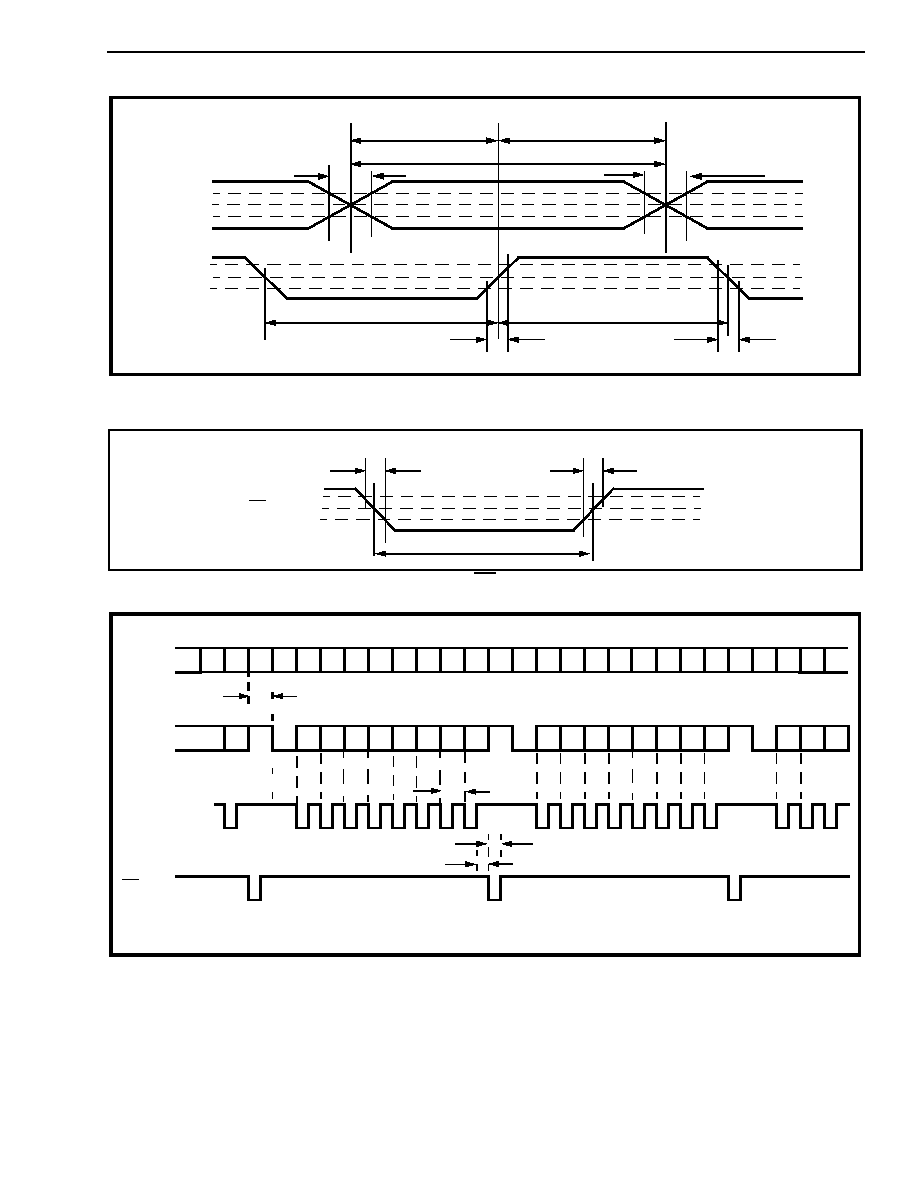
Figure 12 - Serial Data Interface Timing (MODE 0)
DATA
DCLK
t
R
t
DCD
t
CDD
t
DH,
t
DL
t
R
t
F
t
CL
t
CH
t
F
V
HM
V
LM
V
CT
V
HM
V
LM
V
CT
t
RF
t
RR
t
RL
DR
V
HM
V
LM
V
CT
A/B WIRES
DATA
DCLK
DR
stop
start
stop
start
stop
start
stop
start
b0 b1 b2 b3 b4 b5 b6 b7
b7
1
0
b0 b1 b2 b3 b4 b5 b6 b7
1
0
b0 b1 b2
1
0
b7
b0 b1 b2 b3 b4 b5 b6 b7
b0 b1 b2 b3 b4 b5 b6 b7
b0 b1 b2
stop
start
stop
start
t
IDD
t
CRD
1/f
DCLK0
t
RL

Preliminary Information
MT8843
5-37
Figure 15 - Input and Output Timing for BT Caller Display Service (CDS), e.g., CLIP
Notes:
1) By choosing t
GA
=15ms, t
ABS
will be 15-25ms so that the current wetting pulse and AC load can be applied right after the StD falling
edge.
2) SIN227 specifies that the AC and DC loads should be removed between 50-150ms after the end of the FSK signal, indicated by CD
returning to high. The CNIC2 may also be powered down at this time.
3) FSKen should be set low when FSK is not expected to prevent the FSK demodulator from reacting to other in-band signals such as
speech, tone alert signal and DTMF tones.
4) TRIGout is the ring envelope during ringing.
5) The total recognition time is t
REC
= t
GP
+ t
DP
, where t
GP
is the tone present guard time and t
DP
is the tone present detect time (refer
to section "Dual Tone Detection Guard Time" on page 25 for details).
6) The total tone absent time is t
ABS
= t
GA
+ t
DA
, where t
GA
is the tone absent guard time and t
DA
is the tone absent detect time (refer
to section "Dual Tone Detection Guard Time" on page 25 for details).
V
TGt
is the comparator threshold (refer to Figure 4).
Line Reversal
Alerting Signal
Ch. seizure
Mark
Data Packet
Ring
..101010..
Data
t
DP
t
DA
t
GP
t
GA
t
REC
t
ABS
(Note 1)
20±5ms
t
CP
t
CA
A
B
C
D
E
F
G
Zss (Refer to SIN227)
< 0.5mA (optional)
<120
µ
A
Note 2
V
TGt
Note 4
Note 3
A/B Wires
TRIGout
PWDN
ESt
St/GT
StD
TE DC load
TE AC load
FSKen
CD
DR
DCLK
DATA
OSCout
A
100ms
B = 88-110ms
C
45ms (up to 5sec)
D = 80-262ms
E = 45-75ms
F
2.5sec (typ. 500ms)
G > 200ms
Note: All values obtained
from SIN227 Issue 1
Note 5
Note 6
50-150ms
15±1ms
Current wetting pulse (see SIN227)
Preliminary Information
MT8843
5-39
Figure 17 - Input and Output Timing for Bellcore On-hook Data Transmission Associated with
Ringing, e.g., CID
Notes:
This on-hook case application is included because a CIDCW (off-hook) CPE should also be capable of receiving on-hook data
transmission (with ringing) from the end office. TR-NWT-000575 specifies that CIDCW will be offered only to lines which subscribe to
CID.
1) The CPE designer may choose to enable the CNIC2 only after the end of ringing to conserve power in a battery operated CPE. CD is not
activated by ringing.
2) The CPE designer may choose to set FSKen always high while the CPE is on-hook. Setting FSKen low prevents the FSK
demodulator from reacting to other in-band signals such as speech, CAS or DTMF tones.
3) The microcontroller in the CPE powers down the CNIC2 after CD has become inactive.
4) The microcontroller times out if CD is not activated.
1st Ring
2nd Ring
Ch. seizure
Mark
Data Packet
A
C
D
E
F
..101010..
Data
Note 1
Note 2
Note 3
Note 1
Note 4
t
CA
t
CP
B
TIP/RING
TRIGout
PWDN
OSCout
FSKen
CD
DR
DCLK
DATA
A = 2sec typical
B = 250-500ms
C = 250ms
D = 150ms
E = feature specific
Max C+D+E = 2.9 to 3.7sec
F
200ms