 | –≠–ª–µ–∫—Ç—Ä–æ–Ω–Ω—ã–π –∫–æ–º–ø–æ–Ω–µ–Ω—Ç: MT8940AC | –°–∫–∞—á–∞—Ç—å:  PDF PDF  ZIP ZIP |
27
3-27
Æ
Features
∑
Provides T1 clock at 1.544 MHz locked to input
frame pulse
∑
Sources CEPT (30+2) Digital Trunk/ST-BUS
clock and timing signals locked to internal or
external 8 kHz signal
∑
TTL compatible logic inputs and outputs
∑
Uncommitted 2-input NAND gate
∑
Single 5 volt power supply
∑
Low power ISO-CMOS technology
Applications
∑
Synchronization and timing control for T1
and CEPT digital trunk transmission links
∑
ST- BUS clock and frame pulse source
Description
The MT8940 is a dual digital phase-locked loop
providing the timing and synchronization signals for
the T1 or CEPT transmission links and the ST-BUS.
The first PLL provides the T1 clock (1.544 MHz)
synchronized to the input frame pulse at 8 kHz. The
timing signals for the CEPT transmission link and the
ST-BUS are provided by the second PLL locked to
an internal or an external 8 kHz frame pulse signal.
The MT8940 is fabricated in MITEL's ISO-CMOS
technology.
Ordering Information
MT8940AC
24 Pin Ceramic DIP
MT8940AE
24 Pin Plastic DIP
-40∞C to +85∞C
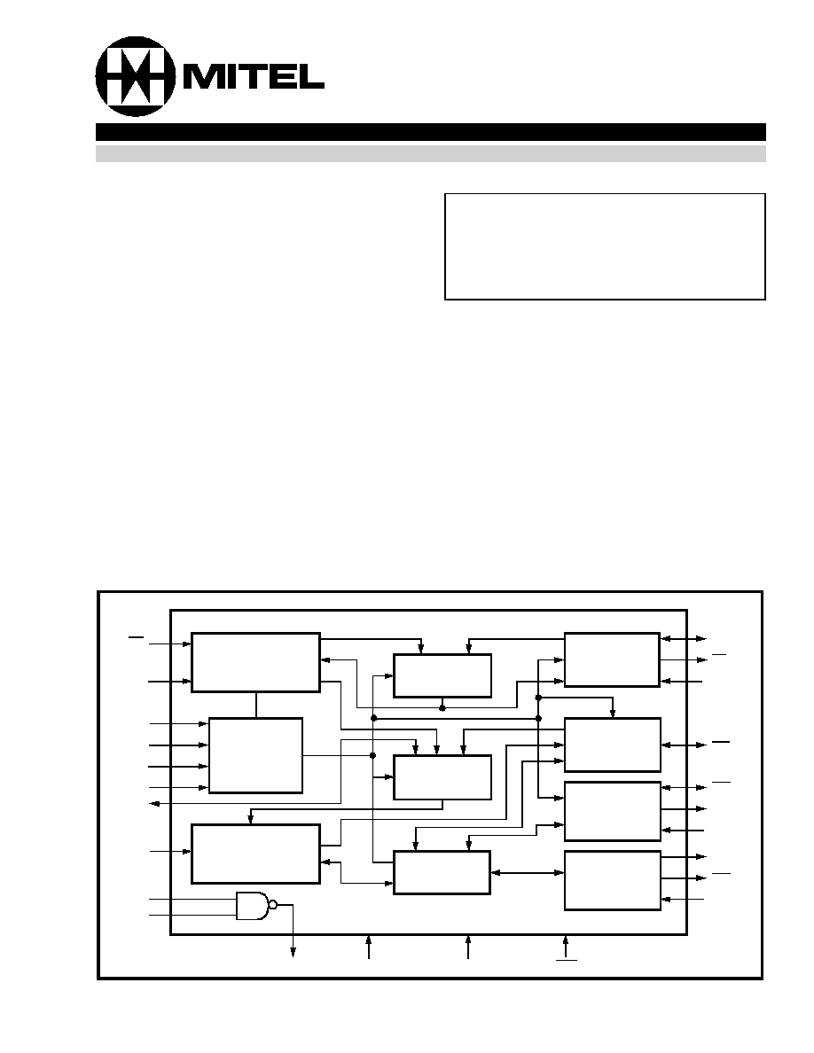
Figure 1 - Functional Block Diagram
F0i
C12i
MS0
MS1
MS2
MS3
C8Kb
C16i
Ai
Bi
Yo
V
DD
V
SS
RST
CVb
CV
ENCV
F0b
C4b
C4o
ENC4o
C2o
C2o
ENC2o
2:1 MUX
Variable
Clock
Control
Mode
Selection
Logic
DPLL #2
Input
Selector
Clock
Generator
Frame Pulse
Control
4.096 MHz
Clock
Control
2.048 MHz
Clock
Control
DPLL #1
ISSUE 7
July 1993
MT8940
T1/CEPT Digital Trunk PLL
ISO-CMOS ST-BUS
TM
FAMILY

MT8940
ISO-CMOS
3-28
Figure 2 - Pin Connections
Pin Description
Pin #
Name
Description
1
EN
CV
Variable clock enable (TTL compatible input) - This input (pulled internally to V
DD
) directly
controls the three states of CV (pin 22) under all modes of operation. When HIGH, enables
CV and when LOW, puts it in high impedance condition. It also controls the three states of
CVb signal (pin 21) if MS1 is LOW. When EN
CV
is HIGH, the pin CVb is an output and when
LOW, it is in high impedance state. However, if MS1 is HIGH, CVb is always an input.
2
MS0
Mode select `0' input (TTL compatible) - This input (pulled internally to V
SS
) in conjunction
with MS1 (pin 4) selects the major mode of operation for both DPLLs. (Refer to Tables 1 and
2).
3
C12i
Clock 12.355 MHz input (TTL compatible) - Master clock input at 12.355 MHz ±100ppm
for DPLL #1.
4
MS1
Mode select-1 input (TTL compatible) - This input (pulled internally to V
SS
) in conjunction
with MS0 (pin 2) selects the major mode of operation for both DPLLs. (Refer to Tables 1 and
2)
5
F0i
Frame pulse input (TTL compatible) - This is the frame pulse input (pulled internally to
V
DD
) at 8 kHz. The DPLL #1 locks to the falling edge of this input to generate T1 (1.544
MHz) clock.
6
F0b
Frame pulse Bidirectional (TTL compatible input and Totem-pole output) - Depending
on the minor mode selected for the DPLL #2, it provides the 8 kHz frame pulse output or acts
as an input (pulled internally to V
DD
) to an external frame pulse.
7
MS2
Mode select-2 input (TTL compatible) - This input (pulled internally to V
DD
) in conjunction
with MS3 (pin 17) selects the minor mode of operation for the DPLL #2. (Refer to Table 3.)
8
C16i
Clock 16.388 MHz input (TTL compatible) - Master clock input at 16.388 MHz±32 ppm for
DPLL #2.
9
EN
C4o
Enable 4.096 MHz clock (TTL compatible input) - This active high input (pulled internally
to V
DD
) enables C4o (pin 11) output. When LOW, the output C4o is in high impedance
condition.
1
2
3
4
5
6
7
8
9
10
11
12
13
14
15
16
24
23
22
21
20
19
18
17
ENVC
MS0
C12i
MS1
F0i
F0b
MS2
C16i
ENC4o
C8Kb
C4o
VSS
VDD
RST
CV
CVb
Yo
Bi
Ai
MS3
ENC2o
C2o
C2o
C4b

ISO-CMOS
MT8940
3-29
10
C8Kb
Clock 8 kHz- Bidirectional (TTL compatible input and open drain output with 100K
internal resistor to V
DD
) - This is the 8 kHz input signal on the rising edge of which DPLL #2
locks during its NORMAL mode. When DPLL #2 is in SINGLE CLOCK mode, this pin outputs
an 8 kHz signal provided by DPLL #1, which is also connected internally to DPLL #2.
11
C4o
Clock 4.096 MHz (Three state output) - This is the inverse of the signal appearing on pin
13 (C4b) at 4.096 MHz and has a rising edge in the frame pulse (F0b) window. The high
impedance state of this output is controlled by EN
C4o
(pin 9).
12
V
SS
Ground (0 Volt)
13
C4b
Clock 4.096 MHz- Bidirectional (TTL compatible input and Totem-pole output) - When
the mode select bit MS3 (pin 17) is HIGH, it provides the 4.096 MHz clock output with the
falling edge in the frame pulse (F0b) window. When pin 17 is LOW, C4b is an input (pulled
internally to V
DD
) to an external clock at 4.096 MHz.
14
C2o
Clock 2.048 MHz (Three state output) - This is the divide by two output of C4b (pin 13) and
has a falling edge in the frame pulse (F0b) window. The high impedance state of this output
is controlled by EN
C2o
(pin 16).
15
C2o
Clock 2.048 MHz (Three state output) - This is the divide by two output of C4b (pin 13) and
has a rising edge in the frame pulse (F0b) window. The high impedance state of this output is
controlled by EN
C2o
(pin 16).
16
EN
C2o
Enable 2.048 MHz clock (TTL compatible input) - This active high input (pulled internally
to V
DD
) enables both C2o and C2o outputs (pins 14 and 15). When LOW, these outputs are
in high impedance condition.
17
MS3
Mode select 3 input (TTL compatible) - This input (pulled internally to V
DD
) in conjunction
with MS2 (pin 7) selects the minor mode of operation for DPLL #2. (Refer to Table 3.)
18,19
Ai, Bi
Inputs A and B (TTL compatible) -These are the two inputs (pulled internally to V
SS
) of the
uncommitted NAND gate
.
20
Y
o
Output Y (Totem pole output) - Output of the uncommitted NAND gate.
21
CVb
Variable clock Bidirectional (TTL compatible input and Totem-pole output) - When
acting as an output (MS1-LOW) during the NORMAL mode of DPLL #1, this pin provides the
1.544 MHz clock locked to the input frame pulse F0i (pin 5). When MS1 is HIGH, it is an
input (pulled internally to V
DD
) to an external clock at 1.544 MHz or 2.048 MHz to provide the
internal signal at 8 kHz to DPLL #2.
22
CV
Variable clock (Three state output) - This is the inverse output of the signal appearing on
pin 21, the high impedance state of which is controlled EN
CV
(pin 1).
23
RST
Reset (Schmitt trigger input) -This input (active LOW) evokes reset condition for the
device.
24
V
DD
V
DD
(+5V) Power supply.
Pin Description (continued)
Pin #
Name
Description

MT8940
ISO-CMOS
3-30
Functional Description
The MT8940 is a dual digital phase-locked loop
providing the timing and synchronization signals to
the interface circuits for T1 and CEPT (30+2)
Primary Multiplex Digital Transmission links. As
shown in Figure 1, it has two digital phase-locked
loops (DPLLs), associated output controls and the
mode selection logic circuits. The two DPLLs,
although similar in principle, operate independently
to provide T1 (1.544 MHz) and CEPT (2.048 MHz)
transmission clocks, and ST-BUS timing signals.
The principle of operation behind the two DPLLs is
shown in Figure 3. A master clock is divided down to
8 kHz where it is compared with the 8 kHz input, and
depending on the output of the phase comparison,
the master clock frequency is corrected. The
MT8940 achieves the frequency correction in both
directions by using the master clock at a slightly
higher frequency and dividing it unaltered or
stretching its period (at two discrete instants in a
frame) before the division depending on the phase
comparison output. When the input frequency is
Figure 3 - DPLL Principle
higher, the unchanged master clock is divided, thus
effectively speeding-up the locally generated clock
and eventually pulling it in synchronization with the
input. If the input frequency is lower than the divided
master clock, the period of the master clock is
stretched by half a cycle, at two discrete instants in a
phase sampling period. This introduces a total delay
of one master clock period over the sampling
duration, which is then divided to generate the local
signal synchronous with the input. Once the output is
phase-locked to the active edge of the input, the
circuit will maintain the locked condition as long as
the input frequency is within the lock-in range (±1.04
Hz) of the DPLLs. The lock-in range is wide enough
to meet the CCITT line rate specification (1.544
MHz±130ppm and 2.048 MHz ±50ppm) for the High
Capacity Terrestrial Digital Service.
Master Clock
(12.355 MHz/
16.388 MHz)
Frequency
Correction
˜
8
Output
(1.544 MHz /
Input (8 kHz)
Phase
Comparison
˜
193 /
˜
256
2.048 MHz)
The phase sampling is done once in a frame (8 kHz)
and the divisions are set at 8 and 193 for DPLL #1,
which locks on to the falling edge of the input at 8
kHz to generate T1 (1.544 MHz) clock. Although the
phase sampling duration is the same for DPLL #2,
the divisions are set at 8 and 256 to provide the
CEPT/ST-BUS clock at 2.048 MHz synchronized to
the rising edge of the input signal (8 kHz). The
master clock source is specified to be at 12.355 MHz
±100 ppm for DPLL #1 and 16.388 MHz ±32 ppm for
DPLL #2 over the entire temperature range of
operation.
The inputs MS0 to MS3 are used to select the
operating mode of the MT8940, see Tables 1 to 4. All
the outputs are individually controlled to the high
impedance condition by their respective enable
controls. The uncommitted NAND gate is available
for use in applications involving MITEL's
MT8976/MH89760 (T1 interfaces) and
MT8979/MH89790 (CEPT interfaces).
Modes of Operation
The operation of the MT8940 is categorized into
major and minor modes. The major modes are
defined for both DPLLs by the mode select pins MS0
and MS1. The minor modes are selected by MS2
and MS3, and are applicable only to DPLL #2. There
are no minor modes for DPLL #1.
Major modes of the DPLL #1
DPLL #1 can be operated in three major modes as
selected by MS0 and MS1 (Table 1). When MS1 is
LOW, it is in NORMAL mode, which provides a T1
(1.544 MHz) clock signal locked to the falling edge of
the input frame pulse F0i (8 kHz). DPLL#1 requires a
master clock input of 12.355 MHz±100 ppm (C12i).
In the second and third major modes (MS1 is HIGH),
DPLL #1 is set to DIVIDE an external 1.544 MHz or
2.048 MHz signal applied at CVb (pin 21). The
division can be set by MS0 to be either 193 (LOW) or
256 (HIGH). In these modes, the 8 kHz output is
connected internally to DPLL #2, which operates in
SINGLE CLOCK mode.
Major modes of the DPLL #2
There are four major modes for DPLL #2 selectable
by MS0 and MS1, as shown in Table 2. In all these
modes DPLL #2 provides the CEPT PCM 30 timing,
and the ST-BUS clock and framing signals.
In NORMAL mode, DPLL #2 provides the CEPT and
ST-BUS compatible timing signals locked to the
rising edge of the 8 kHz input signal (C8Kb). These
ISO-CMOS
MT8940
3-31
signals are the 4.096 MHz (C4o and C4b) and the
2.048 MHz (C2o and C2o) clocks, and the 8 kHz
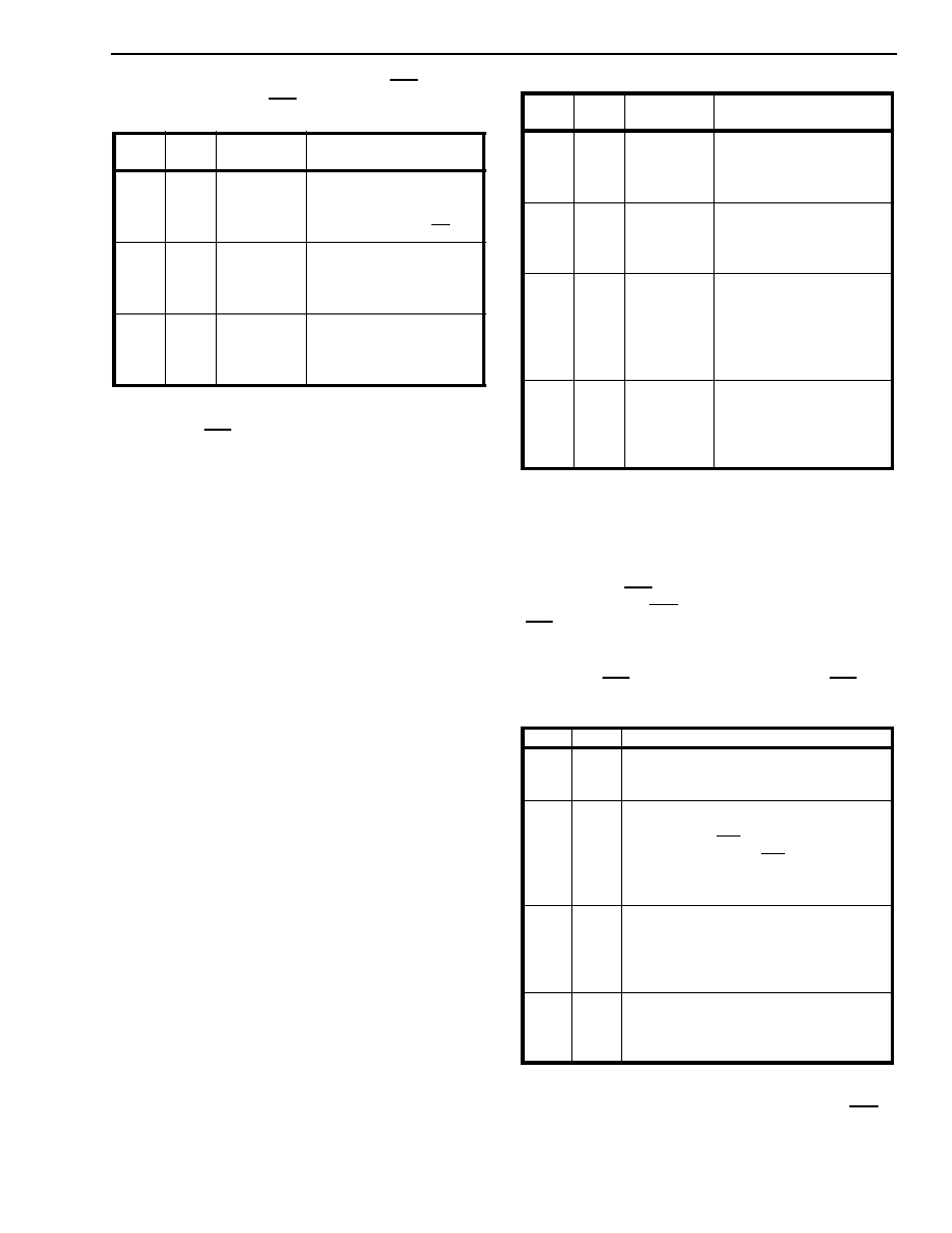
Note: X: indicates don't care
Table 1. Major Modes of the DPLL #1
frame pulse (F0b), which are derived from the 16.388
MHz master clock. This mode can also provide the
ST-BUS timing and framing signals with the input
(C8Kb) tied HIGH and the master clock set at 16.384
MHz. The DPLL makes no correction in this
configuration and provides the timing signals
compatible to the ST-BUS format without any jitter.
In FREE-RUN mode, DPLL #2 generates CEPT and
ST-BUS timing and framing signals with no external
inputs except the master clock set at 16.388 MHz.
Since the master clock source is set at a higher
frequency than the nominal value, the DPLL makes
the necessary corrections to deliver the averaged
timing signals compatible to the ST-BUS format.
The operation of DPLL #2 in SINGLE CLOCK-1
mode is identical to SINGLE CLOCK-2 mode,
providing the CEPT and ST-BUS compatible timing
signals synchronized to the internal 8 kHz signal
obtained from DPLL#1 in DIVIDE mode. When
SINGLE CLOCK-1 mode is selected for DPLL #2, it
automatically selects the DIVIDE-1 mode for DPLL
#1, and thus, an external 1.544 MHz clock signal
applied at CVb (pin 21) is divided by DPLL #1 to
generate the internal signal at 8 kHz onto which
DPLL #2 locks. Similarly when SINGLE CLOCK-2
mode is selected, DPLL #1 is in DIVIDE-2 mode,
with an external signal of 2.048 MHz providing the
internal 8 kHz signal to DPLL #2. In both these
modes, this internal signal is available on C8Kb (pin
10) and DPLL #2 locks to its falling edge to provide
the CEPT and ST-BUS compatible timing signals.
This is in contrast to the Normal mode where these
timing signals are synchronized with the rising edge
of the 8 kHz signal on C8Kb.
Minor modes of the DPLL #2
The minor modes for DPLL #2 depends upon the
status of the mode select bits MS2 and MS3 (pins 7
and 17).
MS0
MS1
Mode of
operation
Function
X
0
NORMAL
Provides the T1 (1.544
MHz) clock synchronized
to the falling edge of the
input frame pulse (F0i).
0
1
DIVIDE-1
DPLL #1 divides the CVb
input by 193. The divided
output is connected to
DPLL #2.
1
1
DIVIDE-2
DPLL #1 divides the CVb
input by 256. The divided
output is connected to
DPLL #2.
Table 2. Major Modes of the DPLL #2
When MS3 is HIGH, DPLL #2 operates in any of the
major modes as selected by MS0 and MS1.
When MS3 is LOW, it overrides the major mode
selected and DPLL #2 accepts an external clock of
4.096 MHz on C4b (pin 13) to provide the 2.048 MHz
clocks (C2o and C2o) and the 8 kHz frame pulse
(F0b) compatible with the ST-BUS format.
The mode select bit MS2, controls the signal
direction of F0b (pin 6). When MS2 is LOW, F0b is an
input for an external frame pulse at 8 kHz. This
Table 3. Minor Modes of the DPLL #2
input is effective only if MS3 is also LOW and C4b is
accepting a 4.096 MHz external clock, which has a
proper phase relationship with the external input on
MS0
MS1
Mode of
operation
Function
0
0
NORMAL
Provides ST-BUS/CEPT
timing signals locked to the
rising edge of the 8kHz
input signal at C8Kb.
1
0
FREE-RUN Provides ST-BUS timing
and framing signals with no
external inputs, except the
master clock.
0
1
SINGLE
CLOCK-1
Provides the CEPT/ST-
BUS compatible timing
signals locked to the falling
edge of the 8kHz internal
signal provided by DPLL
#1.
1
1
SINGLE
CLOCK-2
Provides CEPT/ST-BUS
timing signals locked to the
falling edge of the 8kHz
internal signal provided by
DPLL #1.
MS2
MS3
Functional Description
1
1
Provides ST-BUS 4.096 MHz and 2.048
MHz clocks and 8kHz frame pulse
depending on the major mode selected.
0
1
Provides ST-BUS 4.096 MHz & 2.048 MHz
clocks depending on the major mode
selected while F0b acts as an input.
However, the input on F0b has no effect on
the operation of DPLL #2 unless it is in
FREE-RUN mode.
0
0
Overrides the major mode selected and
accepts properly phase related external
4.096 MHz clock and 8 kHz frame pulse to
provide the ST-BUS compatible clock at
2.048MHz.
1
0
Overrides the major mode selected and
accepts a 4.096 MHz external clock to
provide the ST-BUS clock and frame pulse
at 2.048 MHz and 8 kHz, respectively.