 | –≠–ª–µ–∫—Ç—Ä–æ–Ω–Ω—ã–π –∫–æ–º–ø–æ–Ω–µ–Ω—Ç: MT8950AC | –°–∫–∞—á–∞—Ç—å:  PDF PDF  ZIP ZIP |
6-3
Æ
Features
∑
Transparent coding and decoding of 0 to 8, 9.6
and 19.2 kbps data
∑
Coding compatible to PCM voice channels at
56/64 kbps in ST-BUS format
∑
Automatic line polarity detection and correction
∑
Loopback facility for test purposes
∑
Selectable data formats: RZ or NRZ
∑
Eight user selectable modes of operation
∑
Low power ISO-CMOS technology
Applications
∑
Transparent coder/decoder for synchronous
and asynchronous data
∑
Data terminal (RS-232C, etc.) to ST-BUS
interface
∑
Data switching on digital PBXs
∑
Channel banks/TDM multiplexers
Ordering Information
MT8950AC
24 Pin Ceramic DIP
0∞C to 70∞C
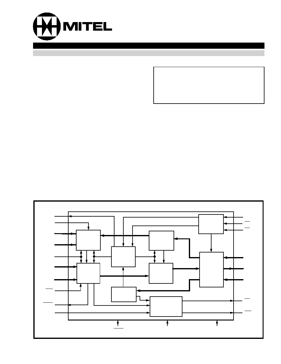
Figure 1 - Functional Block Diagram
DP
SCLK
D
R
1
D
R
2
DF
D
X
1
D
X
2
RxE
NRZo
SPi
PRST
NRZ/RZ
Output
Circuit
NRZ/RZ
Input
Circuit
Timing
& Mode
Control
Control
Register
Decoder
V
DD
Monitoring
Interface
Encoder
Enable
Logic
ST-BUS
Interface
V
SS
C2i
F1i
CA
DSTi
DSTo
CSTi
DA
SPo
ISSUE 4
November 1990
Description
The MT8950 is a coder/decoder which uses the
Transition Encoded Modulation (TEM) technique for
encoding/decoding low speed data to and from a 56/
64 kbps channel (equivalent to PCM Voice). The
coding and decoding scheme is transparent and can
accept either synchronous or asynchronous data up
to 8 kbps (inclusive); at 9.6 kbps and 19.2 kbps.
The MT8950 is fabricated in MITEL's ISO-CMOS
technology.
MT8950
Data Codec
ISO-CMOS ST-BUS
TM
FAMILY

MT8950
ISO-CMOS
6-4
Figure 2 - Pin Connections
Pin Description
Pin #
Name
Description
1
CSTi
Control ST-BUS In (TTL Input) - This ST-BUS interface pin accepts a serial input
stream which loads the Control Register. The mode of operation of the
device, the bits in the Violation word, and, the resetting of Data Activity (DA) and
Scan Point output (SPo) are controlled by this register. The contents of the register
are updated once every ST-BUS frame when the interface is enabled.
2
DSTi
Data ST-BUS In (TTL Input) - Accepts the 8 bits of TEM Data when the ST-BUS
interface is enabled.
3
C2i
2.048 MHz Clock (TTL Input) - This is the input for the 2.048 MHz clock.
4
DSTo
ST-BUS Output (Three-State Output) - This is the 2.048 Mbps serial output for
theTEM encoded word. It is enabled when both F1i and CA are low.
5
F1i
Framing Type 1 Input (TTL Input) - This active low input, in conjunction with CA,
enables the ST-BUS interface (DSTi, DSTo and CSTi). It is internally sampled on
every positive edge of the C2i clock and provides frame synchronization.
6
CA
Control Address (TTL Input) - This active low input (in conjunction with F1i)
enables the ST-BUS interface.
7
DF
Data Format Select (CMOS Input) - When HIGH, the Data Codec accepts and
delivers the data in unipolar Return to Zero (RZ) format. When LOW, the data
format is unipolar NRZ.
8
RxE
Received Energy Signal (Schmitt Input) - When RxE goes LOW it establishes the
polarity of the input pins D
X
1 and D
X
2 in the RZ mode. The input which received the
last pulse before RxE goes LOW is established as the unipolar MARK input. RxE
also enables the operation of DA and SPo outputs the loopback modes (Modes 4, 5
and 6) of the codec, RxE is forced to the LOW state internally independent of the pin
condition. RxE should be exerted LOW for the duration of a data call.
9
D
X
1
Data Transmit 1 (Schmitt Input) - If DF= LOW, accepts data in the NRZ format.
(HIGH = MARK, LOW = SPACE).
If DF=HIGH, accepts active low unipolar pulses representing the digital data in the
RZ format. MARK or SPACE polarity is established by the RxE input.
1
2
3
4
5
6
7
8
9
10
11
12
13
14
15
16
24
23
22
21
20
19
18
17
CSTi
DSTi
C2i
DSTo
F1i
CA
DF
RxE
DX1
DX2
NRZo
VSS
VDD
NC
PRST
NC
NC
DR1
DR2
DA
SPo
SPi
DP
SCLK

ISO-CMOS
MT8950
6-5
10
D
X
2
Data Transmit 2 (Schmitt Input) - If DF = LOW, accepts data pulses which are
encoded only if there is no activity on the D
X
1 pin - the data format and
restrictions on the use of this input is explained in the text.
If DF= HIGH, accepts active low unipolar pulses representing the digital data in the
RZ format. MARK or SPACE polarity is established by the RxE input.
11
NRZo
Non-Return to Zero Output (Open Drain Output) - The incoming data, in the RZ
format or the NRZ format , is internally converted to inverted NRZ and appears on
this open drain output. This output in conjunction with the SPi input can be used for
long space detection.
12
V
SS
Ground (0 Volt).
13
SCLK
Secondary Clock (TTL Input) - This is an external clock input that determines the
timing of the Violation Word and the synchronization pulses. If these features are
not to be utilized, this input can be tied to V
SS
.
14
DP
Drive Point Output (Totem-pole Output) - This output is exerted high when the
Control Register bits b7, b6 and b5 are set to 110 (decimal 6). The operation of the
Codec is normal in every other respect.
15
SPi
Uncommitted Scan Point Input (Voltage Comparator Input ) - A LOW to HIGH
transition on this input causes SPo to be set LOW. This is used to detect a long
SPACE condition in conjunction with NRZo (pin 11).
16
SPo
Uncommitted Scan Point Output (Totem-pole Output ) - This output is set LOW
when the SPi input undergoes a LOW to HIGH transition. The SPo is reset by the
presence of a logic "1" in bit b0 of Control Register. This function is active at all
times except when RxE is false and during power reset conditions.
17
DA
Data Activity (Totem-pole Output ) - The NRZ/RZ input circuitry monitors the
input signal (after polarity is established) and activates this output when it detects a
SPACE on the input. This output is reset by the presence of a logic "1" in bit 1 of the
Control Register. The DA function is active at all times except when RxE is false and
during power reset conditions.
18
D
R
2
Data Receive 2 (Totem-pole Output) - If DF = LOW ( NRZ format), outputs the
secondary data signal in the NRZ form as explained in the text.
If DF = HIGH (RZ format), outputs unipolar, active high MARK pulses.
19
D
R
1
Data Receive 1 (Totem-pole Output) - If DF = LOW (NRZ format) , outputs the
NRZ data signal. ( HIGH = MARK, LOW = SPACE)
If DF = HIGH (RZ format), outputs unipolar, active low SPACE pulses.
20
NC
No connection.
21
NC
No connection.
22
PRST
Power Reset (CMOS Schmitt Input ) - A LOW level on this input evokes the power
reset condition for the codec.
23
NC
No connection.
24
V
DD
Positive
Supply Voltage +5 volts ± 10% .
Pin Description (continued)
Pin #
Name
Description

MT8950
ISO-CMOS
6-6
Theory of Operation
The MT8950 is an encoder/decoder which operates
on low baud rate data (up to 19.2 kbps) to convert it
to the ST-BUS format. The data can subsequently
be transparently switched or transmitted in a manner
identical to PCM encoded voice. In this respect, the
functional characteristics of the device are very
similar to many industry standard voice codecs.
Asynchronous and synchronous data from 0 to 8
kbps and at 9.6 kbps is accepted by the codec
without any restrictions. Asynchronous data at 19.2
kbps should have at least two stop bits for the device
to encode it properly. The data is encoded by the
Codec into an eight bit word which occupies one 64
kbps channel on the ST-BUS. Conversely, it accepts
an encoded 8 bit word from an incoming ST-BUS
stream and regenerates the original digital signal.
Mitel's ST-BUS is a synchronous time division
multiplexed serial stream with a bit rate of 2048
kbps. In a telecommunications environment, it is
generally divided into 32 channels made up of 8 bits
each, with an effective bandwidth of 64 kbps per
channel. These channels may carry data or PCM
encoded voice.
Low Speed Data Format
The Data Codec can accept low speed data in either
Non Return to Zero (NRZ) or Return to Zero (RZ)
format. The NRZ format requires only one line to
carry the data. This format is suitable for interfacing
the data codec with RS-232 type terminals and
microprocessor peripherals such as UARTS, ACIAs,
etc. All signals have to be converted to TTL voltage
levels before being input to the codec.
The RZ format requires two separate lines to
represent the MARKs and SPACEs in the data as
illustrated in Figure 4. This format is useful when the
data terminal is located some distance from the
codec and the data is to be transmitted over a line as
a three level signal (a positive pulse for the
beginning of MARKs, negative pulse for the
beginning of SPACEs and zero level for no change in
the signal). The three level signal is converted to its
TTL-Compatible binary form as shown in Figure 4
before being applied to the codec. A pulse appears
on one line of the input indicating the beginning of
MARKs. This is followed by a pulse on the second
line indicating the beginning of SPACEs. If two or
more pulses appear consecutively on the same line
before the second line of the pair receives or
transmits another pulse, then these pulses can be
considered to be violating the normal rule of the RZ
format and are called "Violation Pulses". The data
codec will accept these violations with the restriction
that the time difference between a violation pulse
Table 1. Summary of Data Codec Capabilities.
Refers to the maximum distortion in the bit period timing of the
regenerated data. (Channel Bandwidth = 64kbps )
Percentage Distortion = |T
BO
- T
BR
|
/
T
BO
X 100
where
T
BO
= Original Data Bit Period
T
BR
= Regenerated Data Bit Period
and an actual data transition be at least 125µs. The
violation pulses can be on the MARK or SPACE line.
In a communications system, these violations can be
used to carry other information when no data is
being transmitted.
Encoding/Decoding Scheme
The Data Codec uses a Transition Encoded
Modulation (TEM) technique to encode low speed
data onto a 56 or 64 kbps equivalent PCM voice
channel. This coding algorithm significantly reduces
data bit distortion. The timing distortion in the
regenerated data is summarized in Table 1. A simple
sampling method for encoding the data would
require a 256 kbps channel to obtain the same low
distortion figures.
If the encoded information is to be transmitted over
digital T1/DS1 trunks, the maximum percentage
distortion in the regenerated data is effectively
doubled. This is due to the fact that the least
significant bit in specific channels on these trunks is
used to transmit signalling information. Thus the
bandwidth per channel is reduced to 56 kbps.
The encoder stage of the Data Codec observes
data transitions in discrete timing windows which are
125µs wide. These timing frames are further divided
into 32 timeslots of 3.906µs duration each (see
Figure 3). The position of the first data transition, the
total number of transitions, and, the time period
between the transitions in this 125µs frame is
encoded as an 8 bit word.
The first five bits (b0 to b4) indicate the position of
the first data transition with respect to the 32
timeslots in the window. Bit 7 in the encoded word
represents the absolute value of the data in the 31st
timeslot. Bits 5 and 6 in conjunction with bit 7 are
used to identify the total number of transitions and
the time period between the transitions. Due to the
fixed bit rate restrictions above 8 kbps, a maximum
Data Rate
Bits/Sec
0 - 8000
9600
19200
Asynchronous
Restrictions
None
None
Minimum
2 Stop Bits
Synchronous
Restrictions
None
None
None
Percentage
Distortion
±3.2
±3.8
±7.5
ISO-CMOS
MT8950
6-7
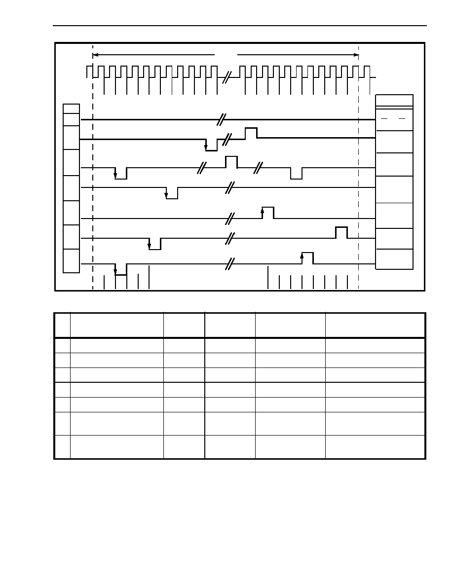
Figure 3 - TEM Coding Scheme
(Note: Waveforms shown are bipolar RZ equivalent of separate RZ/NRZ inputs)
Table 2. TEM Coding Summary
Note: The Level bit (b7) indicates the level (HIGH or LOW) of the input data in timeslot 31 of the current frame.
#
Frame
Description
Level
b7
Frame Type
b6 b5
First Transition
b4 b3 b2 b1 b0
Notes
1
No Pulse
1/0
1 1
1 1 1 1 1
2
2 Data Pulses (T=52 µs)
1/0
1 1
X X X X X
X X X X X
10001 (17)
3
3 Data Pulses (T=52 µs)
1/0
1 1
X X X X X
X X X X X
00100 (4)
4
1 Data Pulse
1/0
1 0
X X X X X
X X X X X = 0 to 31
5
Violation Pulse
1/0
1 0
X X X X X
X X X X X = 0 to 31
6
2 Data Pulses (T=104 µs)
(Timeslot 4 to 31)
1/0
0 1
X X X X X
X X X X X > 00011 (3)
7
2 Data Pulses (T=104 µs)
(Timeslot 0 to 3)
1/0
0 0
Y Y Y X X
XX = 0 to 3
YYY = 0 to 7
b
4
b
3
b
2
b
1
b
0
b
4
b
3
b
2
b
1
b
0
b
4
b
3
b
2
b
1
b
0
b
4
b
3
b
2
b
1
b
0
b
4
b
3
b
2
b
1
b
0
b
1
b
0
b
4
b
3
b
2
b
4
b
3
b
2
b
1
b
0
=11111
125
µ
s
24 25 26 27 28 29 30 31
0
23
22
∑ ∑ ∑
0
1
2
3
4
5
6
7
8
9
10
Internal
Clock
b7
0
b7
-1
Frame Type
b6
b5
1
1
1
1
1
1
1
0
1
0
0
1
0
0
0
0
1
1
1
1
1
1
1
1
1
1
1
1
#
1
2
3
4
5
6
7
0
1
2
3
4
0
1
2
3
4
5
6
7
of seven frames types are possible as shown in
Figure 3. In frame type 7, the first five bits (b0 to b4)
are used to represent two transitions instead of the
normal first transition. Note that the data transitions
in Figure 3 are shown as a three level signal. A
positive transition indicates the beginning of one or
more continuous MARKs and a negative transition
indicates the beginning of one or more continuous
SPACEs.
The decoder stage regenerates the original data
from the 8 bit TEM word. The absolute values of the
data signal in the present and previous frames as
given by b7(n) and b7(n-1) are EX-ORed and the
result in combination with the remaining bits of the
TEM word is used to reproduce the original data with
an accuracy of ± 3.906µs (see Table 2). Due to the
data speed restriction above 8 kbps, the second and
third transitions (if any) will be reproduced at