 | –≠–ª–µ–∫—Ç—Ä–æ–Ω–Ω—ã–π –∫–æ–º–ø–æ–Ω–µ–Ω—Ç: MT8982AN | –°–∫–∞—á–∞—Ç—å:  PDF PDF  ZIP ZIP |
2-31
Æ
Features
∑
ST-BUS/GCI compatible switch matrix
∑
64 channel non-blocking time switch
∑
2 x 32 channel serial inputs and outputs
∑
Per-channel tristate control
∑
4-pin serial microprocessor interface
∑
Patented message mode
∑
Low power consumption (10 mW)
∑
Single 5 volt supply
Applications
∑
Cost sensitive digital switching applications
∑
Digital key telephone systems
∑
GCI/ST-BUS conversion
∑
ST-BUS device control interface
∑
ISDN telephone set support circuit
∑
Interprocessor communication
Description
The MT8982 Small Digital Switch (MiniDX) is a non-
blocking CMOS time switch with a capacity of up to
64 - 8 bit Time Division Multiplexed (TDM) encoded
voice or data channels. It is a size-optimized version
of MITEL's successful MT8980D Digital Switches,
providing switching capability in cost sensitive
applications such as telephone sets and digital key
systems. The TDM interface to the device is via two
pairs of 2048 kbit/s serial streams with 32 64 kbit/s
channels per stream (ST-BUS). A serial microport
provides access to the device for programming the
required connections. The serial microport is
compatible with most common microcontrollers. The
unique message mode capability allows the MT8982
to act as a controller for other members of MITEL's
ST-BUS family of components.
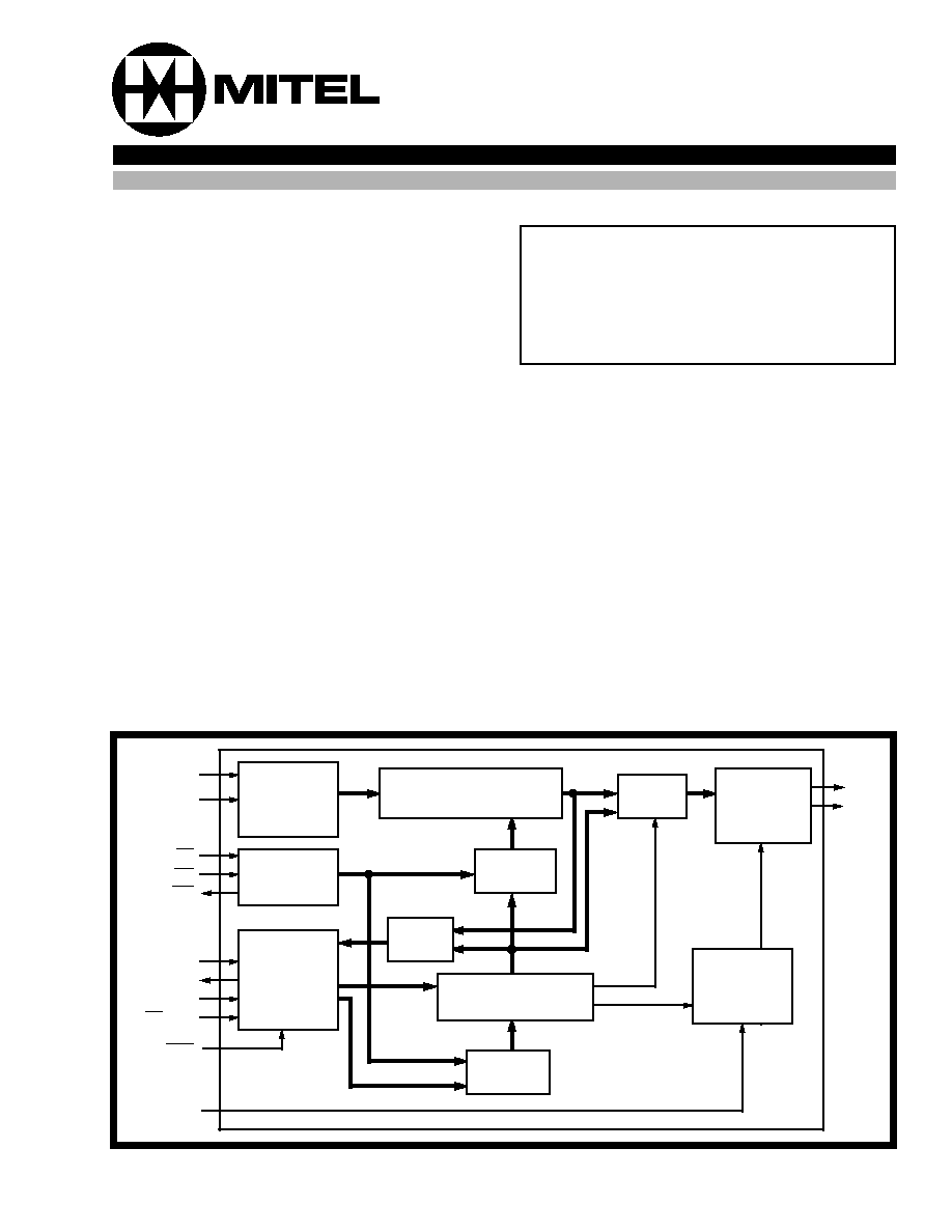
Figure 1 - Functional Block Diagram
STi0
STi1
F0i
C4i
F0o
RxD/CSTi0
TxD/NC
SCLK/CSTi1
CS/CMS
MPS
ODE
STo0
STo1
Serial
to
Parallel
Converter
64 x 8
Data Memory
Output
Mux
Parallel
to
Serial
Converter
Address
Mux
Address
Counters
Serial
Microport
64 x 9
Connect Memory
Address
Mux
3-State
Control
Data
Mux
ISSUE 6
May 1995
MT8982
Small Digital Switch (MiniDX)
ISO-CMOS ST-BUS
TM
FAMILY
Ordering Information
MT8982AC
16 Pin Ceramic DIP
MT8982AE
16 Pin Plastic DIP
MT8982AS
16 Pin SOIC
MT8982AN
20 Pin SSOP
-40 to +85
∞
C
MT8982
ISO-CMOS
2-32
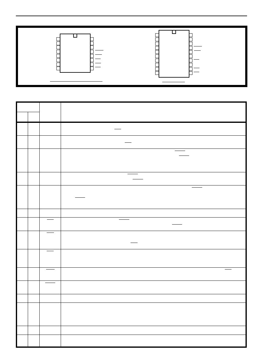
Figure 2 - Pin Connections
Pin Description
Pin #
Name
Description
16
20
1-2
1-2
STi0-
STi1
Serial TDM Input 0 and 1 (Inputs). 2048 kbit/s input data streams containing 32 8-bit
channels synchronized to F0i.
3-4
4-5
STo0-
STo1
Serial TDM Output 0 and 1 (Outputs). 2048 kbit/s output data streams containing 32
8-bit channels synchronized to F0i.
5
6
RxD/
CSTi0
Received Data/Control Stream Input 0 (Input). When MPS is low, this pin receives serial
microport data clocked in by the rising edge SCLK. When MPS is high, this pin receives a
2048 kbit/s serial TDM stream containing 32 8-bit channels, which are written into the
Connect Memory locations corresponding to STo0.
6
7
TxD
Transmit Data (Output). When MPS is low, serial microport data is clocked out on this pin
by the falling edge of SCLK. When MPS is high this output is disabled.
7
9
SCLK/
CSTi1
Serial Microport Clock/Control Stream Input 1 (Input). When MPS is low, this pin
receives a clock which is used to clock data to/from a microcontroller via a serial microport.
When MPS is high, this pin receives a 2048 kbit/s serial TDM stream containing 32 8-bit
channels, which are written into the Connect Memory locations corresponding to STo1.
8
10
V
SS
Power Input. Negative supply (ground).
9
11
CS
Chip Select (Input). When MPS is low, a low on this pin enables the serial microport. A
high on this pin disables RxD and tristates TxD. When MPS is high, this pin must be low.
10
12
C4i
Serial TDM Clock (Input). This clock input is used to clock the TDM data into and out of
the device and refreshes the internal dynamic RAM. The clock rate is 4.096 MHz and data
is clocked in on the rising edge of C4i three-quarters of the way through a bit period.
11
14
F0i
Frame Pulse (Input). This input is the frame synchronization pulse for the 2048 kbit/s
serial TDM streams. It may be either active low stradling the frame boundary (ST-BUS) or
active high at the beginning of timeslot 5 (GCI).
12
16
F0o
Frame Pulse (Output). This pin outputs a frame pulse in the opposite format to F0i (GCI
or ST-BUS) delayed or advanced by five channels.
13
17
MPS
Microport Select (Input). When this pin is held low, the serial microport is in normal mode.
When this pin is high, the microport is in serial bus mode.
14
18
IC
Internal Connection. Tie to V
SS
for normal operation.
15
19
ODE
Output Drive Enable (Input). When this pin is held high, the STo0 and STo1 output drivers
function normally. When this pin is low, STo0 and STo1 are tristated.
NB: When ODE is high, individual channels on STo0 and STo1 can be tristated under
software control.
16
20
V
DD
Power Input. Positive supply.
3,8,
13,15
NC
No Connection.
1
2
3
4
5
6
7
8
16
15
14
13
12
11
10
9
16 PIN CERDIP/PLASTIC/SOIC
STi0
STi1
STo0
STo1
RxD/CSTi0
TxD/NC
SCLK/CSTi1
VSS
VDD
ODE
IC
MPS
F0o
F0i
C4i
CS
1
2
3
4
5
6
7
8
9
10
11
12
20
19
18
17
16
15
14
13
STi0
STi1
NC
STo0
STo1
RxD/CSTi0
TxD/NC
NC
SCLK/CSTi1
VSS
20 PIN SSOP
VDD
ODE
IC
MPS
NC
F0i
NC
C4i
CS
F0o

ISO-CMOS
MT8982
2-33
Functional Description
The MT8982 (MiniDX) provides cost effective time
switching capability for small size applications
utilizing up to two serial Time Division Multiplexed
(TDM) streams. Each TDM stream consists of 32 64
kb/s channels, giving the MiniDX a maximum
capacity of 64 channels. The input framing signal
may be either a ST-BUS or a GCI frame pulse. The
MT8982 will output a delayed or advanced frame
pulse in the opposite format to permit conversion
between the two formats.
The MiniDX can switch data from any channel in one
of the two serial input TDM streams to any channel in
either of the two serial output TDM streams. The
microcontroller controlling the MiniDX writes to the
MT8982 Connect Memory to establish the
connection between the required input TDM channel
and the selected output TDM channel(s). By reading
the Connect Memory the microcontroller can check
switched connections which have already been
established.
The MiniDX can also operate in message mode
where the microcontroller transmits the data on the
TDM serial stream. The microcontroller writes to the
MT8982 Connect Memory to transmit data on the
required output TDM channels. Reading the Data
Memory of the MT8982 allows the microcontroller to
receive messages from TDM input channels. These
operations are useful for control of other ST-BUS
components or for interprocessor communication.
Hardware Description
TDM Interface
The MT8982 continuously receives TDM serial data
at 2048 kbit/s through two serial inputs. These serial
streams are then converted into a parallel format and
stored sequentially in a 64x8 bit Data Memory. The
sequential addressing is generated by an internal
counter that is reset by the input 8 kHz frame pulse
(F0i) which marks the frame boundaries of the
incoming serial data stream. This counter increments
with each timeslot so that it matches the binary count
of the timeslot of the incoming data. The TDM
timeslot count always corresponds to the ST-BUS
channel positions. An extra address bit is used to
differentiate between the two input data streams.
The input 8 kHz frame pulse may be either ST-BUS
or GCI formatted. A ST-BUS formatted frame pulse
is an active low signal which straddles the frame
boundary. It idles high the rest of the time. A GCI
formatted frame pulse is active high at the beginning
of timeslot 5 (relative to the MT8982) and idles low.
The MT8982 automatically determines the type of
frame pulse from the level of the idle over five clock
periods. A ST-BUS formatted frame pulse resets the
internal address counters to zero. A GCI formatted
frame pulse resets the counters to five.
F0o outputs a frame pulse in the opposite format. If
F0i is a ST-BUS formatted frame pulse, F0o will be a
GCI formatted frame pulse delayed by five channels
after F0i. If F0i is a GCI formatted frame pulse, F0o
will be a ST-BUS formatted frame pulse delayed by
27 channels (32-5).
During normal operation every second falling edge of
the clock marks a timeslot boundary and the input
data is clocked in by the rising edge, three-quarters
of the way into the bit cell. The master clock must
be 4.096 MHz for the F0o signal to be valid and to
receive a GCI formatted F0i.
Data which is output onto a TDM serial output
channel may come from two sources; the Data
Memory or the Connect Memory. If a channel is
configured in connection mode, the source of output
data is the Data Memory. If a channel is configured
in message mode, the source of the output data is
the Connect Memory. Data destined for a particular
channel on the serial output links is read from the
data or connect memory in the previous channel
timeslot. This allows for delay in RAM access and
parallel-to-serial conversion. Each output data
channel can also be placed in tristate mode.
When an output channel is in connection mode, the
TDM output data is read from a Data Memory
location pointed to by an address stored in the 64x8
bit Connect Memory. The Connect Memory
locations are addressed sequentially, with each
location corresponding to an output TDM link/
channel. In the channel time before the data is to be
output, the contents of each Connect Memory
location are output to the address bus of the Data
Memory. The contents of the Data Memory at the
selected address are then transferred to the parallel-
to-serial converter. The parallel-to-serial converter
outputs onto the TDM serial stream during the
correct channel time. By having the output channel
specify the input channel, the user can route the
same input channel to several output channels. This
function is useful for broadcasting or resource
channel uses.

MT8982
ISO-CMOS
2-34
When an output channel is in message mode, the
data for the output channel originates from the
microcontroller. The microcontroller writes data to
the Connect Memory location which corresponds to
the output link and channel number. The contents of
the Connect Memory are transferred directly to the
serial-to-parallel converter one channel time before it
is to be output. The Connect Memory data is output
MSB first, repetitively once per frame, until it is
changed by the microcontroller.
If the output channel is configured in tristate mode,
the TDM serial stream output will be placed in high
impedance during that channel time. This mode is
entered by configuring the channel into connection
mode and then setting the tristate control bit. All
channels on both output TDM streams can be
tristated by pulling pin 16 (ODE) low. This overrides
the individual channel programming.
The Data and Connect Memories are dynamic
memories. They are refreshed by the sequential
addressing generated by C4i.
Microcontroller Interface
The MT8982 is controlled via a synchronous, serial
microport. The microport is compatible with Intel's
MCS-51 serial port Mode 0 specifications, Motorola's
Serial Peripheral Interface (SPI) specifications, and
National's MicroWire specifications. The port
consists of a transmit data line (TxD), a receive data
line (RxD), a chip select line (CS), and a
synchronous clock input (SCLK). All memory
locations and control functions on the MiniDX are
accessed through this port. The microport may also
be configured in serial bus mode where data is
clocked into the Connect Memory in the same way
as STi0 and STi1 are clocked into Data Memory.
In serial microport mode, CS must be low to enable a
microport access. SCLK clocks the serial microport
data in or out through RxD and TxD, LSB first. The
TxD output driver is tristated when it is inactive. This
allows RxD and TxD to be connected together for a
single TxD/RxD line as used in the INTEL MCS-51
microcontrollers. Figure 3 shows a serial microport
access cycle.
A microport access cycle (microcycle) begins with a
falling edge on CS. Eight bits of data are clocked
into RxD by the rising edge of SCLK. Two of these
eight bits indicate whether the microcycle operation
is a read or a write, the rest of the bits are used for
addressing. These eight bits are defined as the
command/ address byte (Table 1). If the microcyle
operation is a write, another eight bits are clocked
Figure 3 - Serial Microport Timing
D
0
D
1
D
2
D
3
D
4
D
5
D
6
D
7
D
0
D
1
D
2
D
3
D
4
D
5
D
6
D
7
D
0
D
1
D
2
D
3
D
4
D
5
D
6
D
7
D
0
D
1
D
2
D
3
D
4
D
5
D
6
D
7
D
0
D
1
D
2
D
3
D
4
D
5
D
6
D
7
RxD
TxD
SCLK
CS
Minimum delay between accesses equals 3.0
µ
sec.
The Mini Dx:
- latches received data in on the rising edge of SCLK
The falling edge of CS indicates that a COMMAND/ADDRESS byte will be transmitted. Subsequent byte is always data.
Subsequent write microcycles may flow without raising CS. CS must go high after a read microcycle.
COMMAND/ADDRESS
DATA INPUT/OUTPUT
COMMAND/ADDRESS
- outputs transmit data on the falling edge of SCLK

ISO-CMOS
MT8982
2-35
into RxD by the rising edges of the next eight SCLK
cycles. If the operation is a read, eight data bits are
clocked from TxD by the falling edges of the next
eight SCLK cycles. The rising edge of CS tristates
TxD after the last transmitted bit.
Successive write microcycles can take place while
CS remains low, with each microcycle following the
sequence of a command/address byte followed by a
data byte. CS must go high after a read microcycle.
Note that a command/address byte must always
follow the high to low transition on CS.
When the MPS input is pulled high and the CS input
is pulled low, the microport is put into serial bus
mode. Pins RxD and SCLK become CSTi0 and
CSTi1, respectively, and are configured as 2048 kbit/
s serial streams with 32 channels each. The frame
and timeslot boundaries are determined by F0i and
C4. Each channel on CSTi0 and CSTi1 is stored in
the connect memory address corresponding to the
link and channel number. The Data Memory and the
Connect Memory cannot be read when the microport
is in serial bus mode.
Device Timing
During each TDM timeslot, eight read or write
operations occur internally in the MT8982. These are
shown in Figure 4. During the first two bit periods,
data received in the previous timeslot on the two
input TDM streams is loaded into the Data Memory.
Bit periods 2 and 6 are serial microport access
windows; data may be read from, or written to any
accessible memory location. During bit periods 3
and 5, data is read from the connect memory for the
next timeslot on links 0 and 1 respectively. The Data
Memory locations which are addressed by the
previous reads of the connect memory are accessed
during bit periods 4 and 7.
When the microport is in serial bus mode, bit periods
2 and 6 have a slightly different function. Data from
the previous timeslot of CSTi0 and CSTi1
respectively is written to the corresponding connect
memory locations.
The transfer of information from the input TDM
streams to the output TDM streams results in a delay
through the MT8982. This delay is dependent only
on the combination of source and destination
Table 1. Command Address Byte
Table 2. Connect Memory Connection Mode Data Byte
Bit
Name
Description
7
Stream
Stream. This is the most significant bit of the address for the memory location that
is to be accessed. It corresponds to one of the TDM serial streams (0-1).
2-6
Ch0-Ch4
Channel 0-4. These bits are the five least significant bits of the address for the
memory location that is to be accessed. The binary value of these bits correspond
to a TDM channel (0-31).
0-1
Cmd0-Cmd1
Command Select 0-1. These two bits define the four command operations for the
MT8982. The destination addressed by the command is defined in bits 2-7 of the
Command/Address byte.
Cmd0-Cmd1
0-0
Read from Connect Memory.
0-1
Write to Connect Memory and set connection mode.
1-0
Read Data Memory.
1-1
Write to Connect Memory and set message mode.
Bit
Name
Description
7
NA
Unused.
6
ODE
Output Drive Enable. When this bit is set, the addressed TDM channel is placed
in tristate. When low, the output is enabled.
5
STi
Input Stream. This bit defines the input TDM stream from which the output data is
sourced (0-1).
0-4
SC0-SC4
Source Channel 0-4. The binary value of these bits defines the input channel from
which the output data is sourced (0-31).