 | –≠–ª–µ–∫—Ç—Ä–æ–Ω–Ω—ã–π –∫–æ–º–ø–æ–Ω–µ–Ω—Ç: MT9044AP | –°–∫–∞—á–∞—Ç—å:  PDF PDF  ZIP ZIP |
1
MT9044
T1/E1/OC3 System Synchronizer
Features
∑
Supports AT&T TR62411 and Bellcore
GR-1244-CORE Stratum 3, Stratum 4
Enhanced and Stratum 4 timing for DS1
interfaces
∑
Supports ITU-T G.812 Type IV clocks for 1,544
kbit/s interfaces and 2,048 kbit/s interfaces
∑
Supports ETSI ETS 300 011, TBR 4, TBR 12
and TBR 13 timing for E1 interfaces
∑
Selectable 1.544MHz, 2.048MHz or 8kHz input
reference signals
∑
Provides C1.5, C2, C3, C4, C6, C8, C16, and
C19 (STS-3/OC3 clock divided by 8) output
clock signals
∑
Provides 5 different styles of 8 KHz framing
pulses
∑
Holdover frequency accuracy of 0.05 PPM
∑
Holdover indication
∑
Attenuates wander from 1.9Hz
∑
Provides Time Interval Error (TIE) correction
∑
Accepts reference inputs from two independent
sources
∑
JTAG Boundary Scan
Applications
∑
Synchronization and timing control for
multitrunk T1,E1 and STS-3/OC3 systems
∑
ST-BUS clock and frame pulse sources
Description
The MT9044 T1/E1/OC3 System Synchronizer
contains a digital phase-locked loop (DPLL), which
provides timing and synchronization signals for
multitrunk T1 and E1 primary rate transmission links
and STS-3/0C3 links.
The MT9044 generates ST-BUS clock and framing
signals that are phase locked to either a 2.048MHz,
1.544MHz, or 8kHz input reference.
The MT9044 is compliant with AT&T TR62411 and
Bellcore GR-1244-CORE Stratum 3, Stratum 4
Enhanced, and Stratum 4; and ETSI ETS 300 011. It
will meet the jitter/wander tolerance, jitter/wander
transfer, intrinsic jitter/wander, frequency accuracy,
capture range, phase change slope, holdover
frequency and MTIE requirements for these
specifications.
Ordering Information
MT9044AP
44 Pin PLCC
MT9044AL
44 Pin MQFP
-40 to +85
∞
C
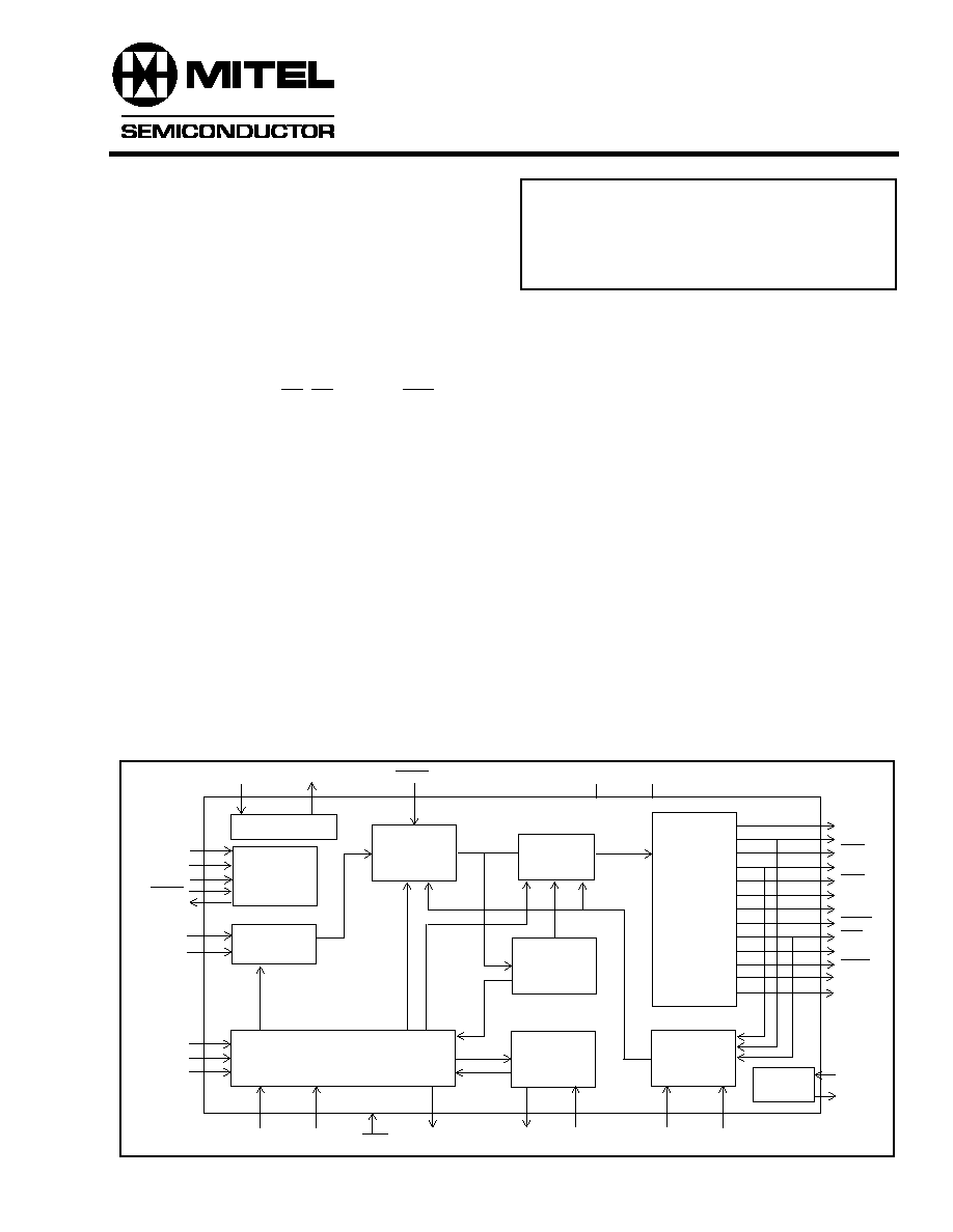
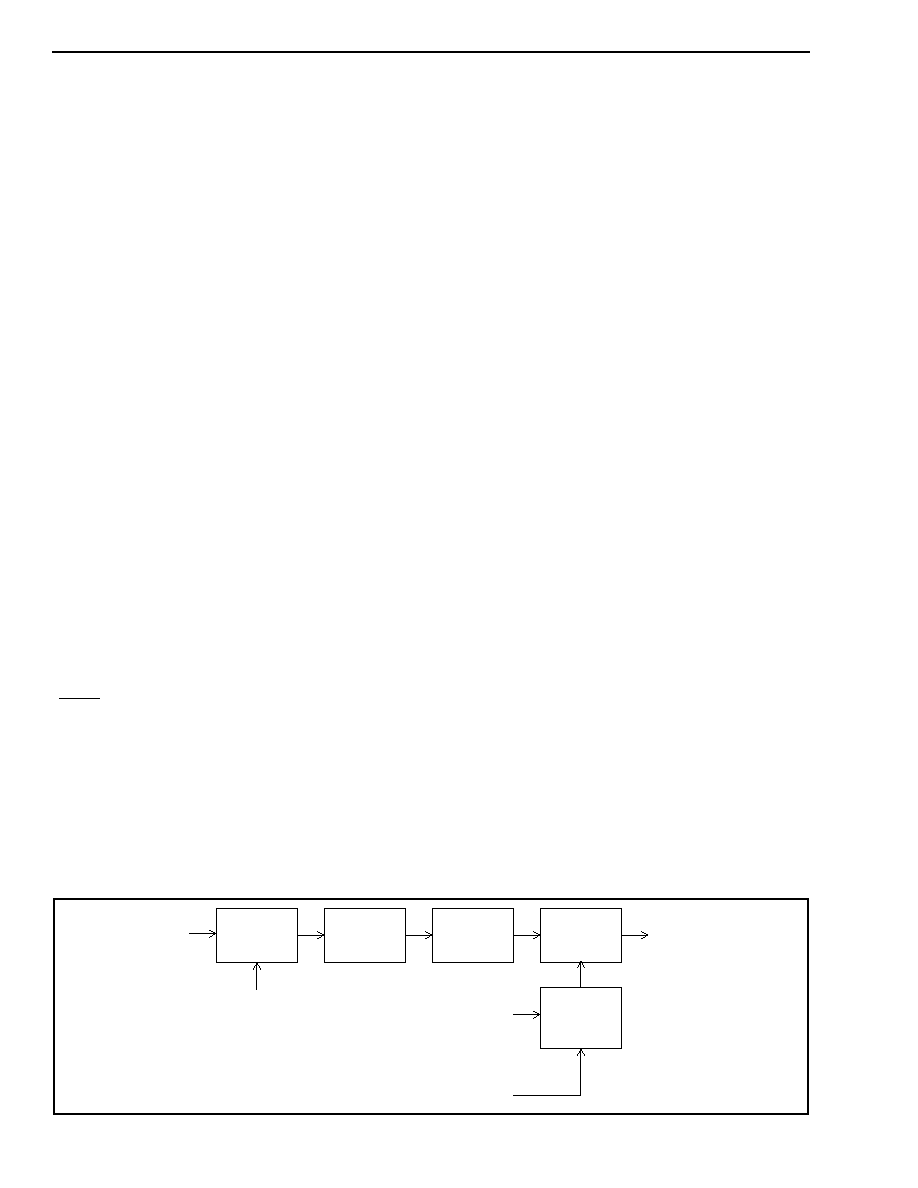
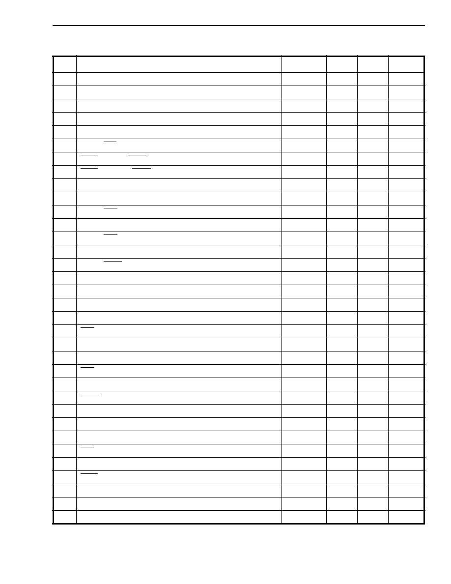
Figure 1 - Functional Block Diagram
MS1
MS2
GTo
GTi
FS1
FS2
TCK
SEC
RST
RSEL
LOS1
LOS2
VDD
VSS
TCLR
C3o
C1.5o
C2o
C4o
C8o
C16o
F0o
F8o
F16o
OSCo
OSCi
C19o
TDO
PRI
TDI
TMS
TRST
C6o
RSP
TSP
ACKi
ACKo
HOLDOVER
Output
Interface
Circuit
Frequency
Select
MUX
Master Clock
APLL
Feedback
Guard Time
Circuit
State
Select
Input
Impairment
Monitor
Virtual
Reference
DPLL
TIE
Corrector
Circuit
State
Select
IEEE
1149.1a
Automatic/Manual
Control State Machine
Reference
Select
MUX
Reference
Select
TIE
Corrector
Enable
Selected
Reference
DS5058
ISSUE 3
September 1999
Advance Information
MT9044
Advance Information
2
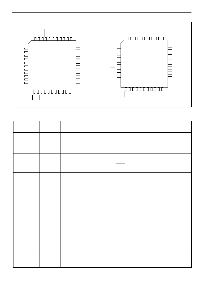
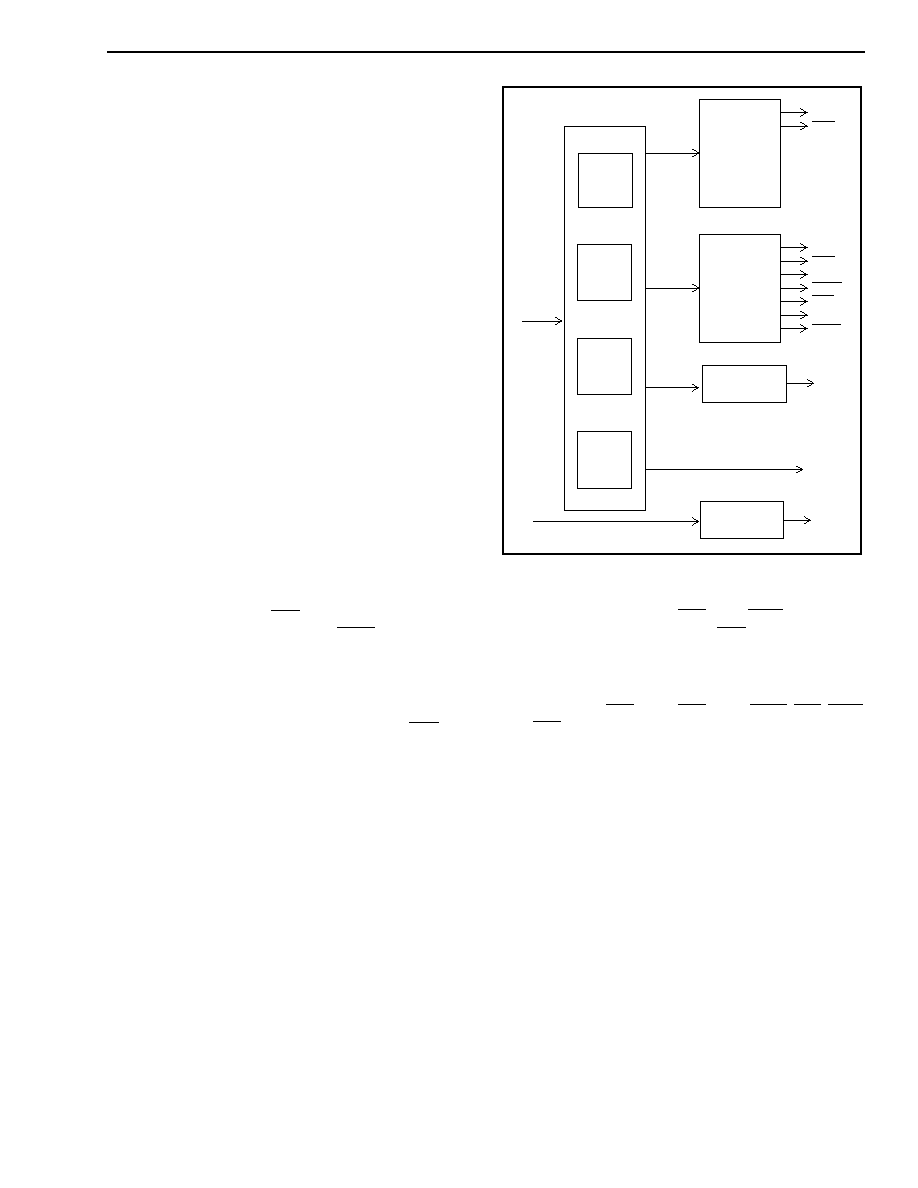
Figure 2 - Pin Connections
Pin Description
Pin #
PLCC
Pin #
MQFP
Name
Description
1,10,
23,31
39,4,17
,25
V
SS
Ground. 0 Volts.
2
40
TCK
Test Clock (TTL Input): Provides the clock to the JTAG test logic. This pin is
internally pulled up to V
DD
.
3
41
TCLR
TIE Circuit Reset (TTL Input): A logic low at this input resets the Time Interval
Error (TIE) correction circuit resulting in a re-alignment of input phase with output
phase as shown in Figure 19. The TCLR pin should be held low for a minimum of
300ns. This pin is internally pulled down to VSS.
4
42
TRST
Test Reset (TTL Input): Asynchronously initializes the JTAG TAP controller by
putting it in the Test-Logic-Reset state. This pin is internally pulled down to VSS.
5
43
SEC
Secondary Reference (TTL Input). This is one of two (PRI & SEC) input
reference sources (falling edge) used for synchronization. One of three possible
frequencies (8kHz, 1.544MHzMHz, or 2.048MHz) may be used. The selection of
the input reference is based upon the MS1, MS2, LOS1, LOS2, RSEL, and GTi
control inputs (Automatic or Manual). This pin is internally pulled up to V
DD
.
6
44
PRI
Primary Reference (TTL Input). See pin description for SEC. This pin is
internally pulled up to V
DD
.
7,28
1,22
V
DD
Positive Supply Voltage. +5V
DC
nominal.
8
2
OSCo
Oscillator Master Clock (CMOS Output). For crystal operation, a 20MHz crystal
is connected from this pin to OSCi, see Figure 10. For clock oscillator operation,
this pin is left unconnected, see Figure 9.
9
3
OSCi
Oscillator Master Clock (CMOS Input). For crystal operation, a 20MHz crystal is
connected from this pin to OSCo, see Figure 10. For clock oscillator operation, this
pin is connected to a clock source, see Figure 9.
11
5
F16o
Frame Pulse ST-BUS 8.192 Mb/s (CMOS Output). This is an 8kHz 61ns active
low framing pulse, which marks the beginning of an ST-BUS frame. This is typically
used for ST-BUS operation at 8.192 Mb/s. See Figure 20.
1
8
7
4 3
9
10
11
12
37
33
34
35
36
38
39
40
41
42
VSS
TCLR
SEC
PRI
VDD
OSCo
OSCi
F16o
F0o
F8o
C1.5o
GTi
GTo
LOS2
LOS1
MS2
MS1
RSEL
FS2
FS1
RST
18 19 20 21 22 23 24
A
CKi
VSS
C8o
C16
o
C4o
C19o
MT9044
2
5
6
43
44
32
31
30
29
25 26 27 28
13
14
15
16
17
TCK
TRST
TMS
TDI
TEST
VSS
TDO
C2o
C6o
AC
K
o
VDD
C3o
AVDD
TSP
RSP
VSS
HOLDOVER
39
2
1
42 41
3
4
5
6
31
27
28
29
30
32
33
34
35
36
VSS
TCLR
SEC
PRI
VDD
OSCo
OSCi
F16o
F0o
F8o
C1.5o
GTi
GTo
LOS2
LOS1
MS2
MS1
RSEL
FS2
FS1
RST
12 13 14 15 16 17 18
A
CKi
VSS
C8o
C16
o
C4o
C19o
MT9044AL
40
43
44
37
38
26
25
24
19 20 21 22
7
8
9
10
11
TCLK
TRST
TMS
TDI
HOLDOVER
TEST
VSS
TDO
C2o
C6o
AC
K
o
VDD
C3o
AVDD
TSP
RSP
VSS
23
Advance Information
MT9044
3
12
6
RSP
Receive Sync Pulse (CMOS Output). This is an 8kHz 488ns active high framing
pulse, which marks the end of an ST-BUS frame. This is typically used for
connection to the Siemens MUNICH-32 device. See Figure 21.
13
7
F0o
Frame Pulse ST-BUS 2.048Mb/s (CMOS Output). This is an 8kHz 244ns active
low framing pulse, which marks the beginning of an ST-BUS frame. This is typically
used for ST-BUS operation at 2.048Mb/s and 4.096Mb/s. See Figure 20.
14
8
TSP
Transmit Sync Pulse (CMOS Output). This is an 8kHz 488ns active high framing
pulse, which marks the beginning of an ST-BUS frame. This is typically used for
connection to the Siemens MUNICH-32 device. See Figure 21.
15
9
F8o
Frame Pulse (CMOS Output). This is an 8kHz 122ns active high framing pulse,
which marks the beginning of a frame. See Figure 20.
16
10
C1.5o
Clock 1.544MHz (CMOS Output). This output is used in T1 applications.
17
11
AVdd
Analog Vdd. +5V
DC
nominal.
18
12
C3o
Clock 3.088MHz (CMOS Output). This output is used in T1 applications.
19
13
C2o
Clock 2.048MHz (CMOS Output). This output is used for ST-BUS operation at
2.048Mb/s.
20
14
C4o
Clock 4.096MHz (CMOS Output). This output is used for ST-BUS operation at
2.048Mb/s and 4.096Mb/s.
21
15
C19o
Clock 19.44MHz (CMOS Output). This output is used in OC3/STS3 applications.
22
16
ACKi
Analog PLL Clock Input (CMOS Input). This input clock is a reference for an
internal analog PLL. This pin is internally pulled down to VSS.
24
18
ACKo
Analog PLL Clock Output (CMOS Output). This output clock is generated by
the internal analog PLL.
25
19
C8o
Clock 8.192MHz (CMOS Output). This output is used for ST-BUS operation at
8.192Mb/s.
26
20
C16o
Clock 16.384MHz (CMOS Output). This output is used for ST-BUS operation with
a 16.384MHz clock.
27
21
C6o
Clock 6.312 Mhz (CMOS Output). This output is used for DS2 applications.
29
23
HOLDOVER Holdover (CMOS Output). This output goes to a logic high whenever the digital
PLL goes into holdover mode.
30
24
GTi
Guard Time (Schmitt Input). This input is used by the MT9044 state machine in
both Manual and Automatic modes. The signal at this pin affects the state changes
between Primary Holdover Mode and Primary Normal Mode, and Primary
Holdover Mode and Secondary Normal Mode. The logic level at this input is gated
in by the rising edge of F8o. See Tables 4 and 5.
32
26
GTo
Guard Time (CMOS Output). The LOS1 input is gated by the rising edge of F8o,
buffered and output on GTo. This pin is typically used to drive the GTi input through
an RC circuit.
33
27
LOS2
Secondary Reference Loss (TTL Input). This input is normally connected to the
loss of signal (LOS) output signal of a Line Interface Unit (LIU). When high, the
SEC reference signal is lost or invalid. LOS2, along with the LOS1 and GTi inputs
control the MT9044 state machine when operating in Automatic Control. The logic
level at this input is gated in by the rising edge of F8o. This pin is internally pulled
down to VSS.
Pin Description (continued)
Pin #
PLCC
Pin #
MQFP
Name
Description

MT9044
Advance Information
4
34
28
LOS1
Primary Reference Loss (TTL Input). Typically, external equipment applies a
logic high to this input when the PRI reference signal is lost or invalid. The logic
level at this input is gated in by the rising edge of F8o. See LOS2 description. This
pin is internally pulled down to VSS.
35
29
TDO
Test Serial Data Out (TTL Output). JTAG serial data is output on this pin on the
falling edge of TCK. This pin is held in high impedance state when JTAG scan is
not enable.
36
30
MS2
Mode/Control Select 2 (TTL Input). This input, in conjunction with MS1,
determines the device's mode (Automatic or Manual) and state (Normal, Holdover
or Freerun) of operation. The logic level at this input is gated in by the rising edge
of F8o. See Table 3.
37
31
MS1
Mode/Control Select 1 (TTL Input). The logic level at this input is gated in by the
rising edge of F8o. See pin description for MS2. This pin is internally pulled down
to VSS.
38
32
RSEL
Reference Source Select (TTL Input). In Manual Control, a logic low selects the
PRI (primary) reference source as the input reference signal and a logic high
selects the SEC (secondary) input. In Automatic Control, this pin must be at logic
low. The logic level at this input is gated in by the rising edge of F8o. See Table 2.
This pin is internally pulled down to VSS.
39
33
TEST
Test (TTL Input). This input is normally tied low. When pulled high, it enables
internal test modes. This pin is internally pulled down to VSS.
40
34
FS2
Frequency Select 2 (TTL Input). This input, in conjunction with FS1, selects
which of three possible frequencies (8kHz, 1.544MHz, or 2.048MHz) may be input
to the PRI and SEC inputs. See Table 1.
41
35
FS1
Frequency Select 1 (TTL Input). See pin description for FS2.
42
36
TDI
Test Serial Data In (TTL Input). JTAG serial test instructions and data are shifted
in on this pin. This pin is internally pulled up to V
DD
.
43
37
RST
Reset (Schmitt Input). A logic low at this input resets the MT9044. To ensure
proper operation, the device must be reset after changes to the method of control,
reference signal frequency changes and power-up. The RST pin should be held
low for a minimum of 300ns. While the RST pin is low, all frame and clock outputs
are at logic high. Following a reset, the input reference source and output clocks
and frame pulses are phase aligned as shown in Figure 19.
44
38
TMS
Test Mode Select (TTL Input). JTAG signal that controls the state transitions of
the TAP controller. This pin is internally pulled up to V
DD
.
Pin Description (continued)
Pin #
PLCC
Pin #
MQFP
Name
Description
Advance Information
MT9044
5
Functional Description
The MT9044 is a Multitrunk System Synchronizer,
providing timing (clock) and synchronization (frame)
signals to interface circuits for T1 and E1 Primary
Rate Digital Transmission links.
Figure 1 shows the functional block diagram which is
described in the following sections.
Reference Select MUX Circuit
The MT9044 accepts two simultaneous reference
input signals and operates on their falling edges.
Either the primary reference (PRI) signal or the
secondary reference (SEC) signal can be selected
as input to the TIE Corrector Circuit. The selection is
based on the Control, Mode and Reference
Selection of the device. See Tables 1, 4 and 5.
Frequency Select MUX Circuit
The MT9044 operates with one of three possible
input reference frequencies (8kHz, 1.544MHz or
2.048MHz). The frequency select inputs (FS1 and
FS2) determine which of the three frequencies may
be used at the reference inputs (PRI and SEC). Both
inputs must have the same frequency applied to
them. A reset (RST) must be performed after every
frequency select input change. Operation with FS1
and FS2 both at logic low is reserved and must not
be used. See Table 1.
Table 1 - Input Frequency Selection
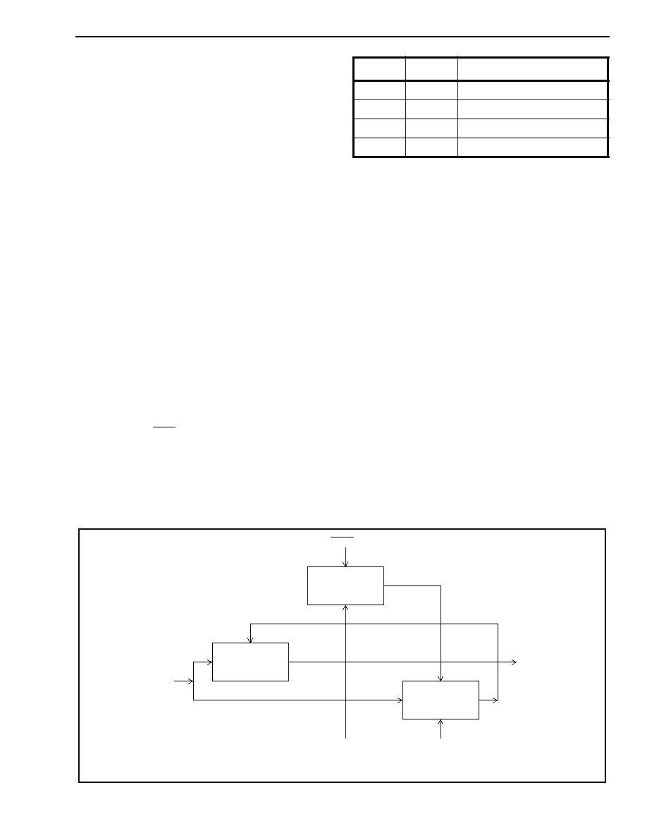
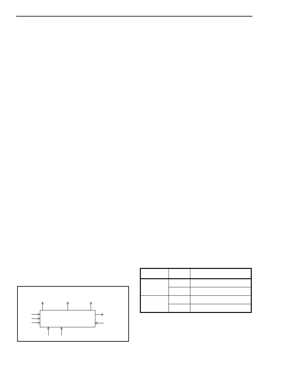
Time Interval Error (TIE) Corrector Circuit
The TIE corrector circuit, when enabled, prevents a
step change in phase on the input reference signals
(PRI or SEC) from causing a step change in phase at
the input of the DPLL block of Figure 1.
During reference input rearrangement, such as
during a switch from the primary reference (PRI) to
the secondary reference (SEC), a step change in
phase on the output signals will occur. A phase step
at the input of the DPLL will lead to unacceptable
phase changes in the output signal.
As shown in Figure 3, the TIE Corrector Circuit
receives one of the two reference (PRI or SEC)
signals, passes the signal through a programmable
delay line, and uses this delayed signal as an
internal virtual reference, which is input to the DPLL.
Therefore, the virtual reference is a delayed version
of the selected reference.
During a switch, from one reference to the other, the
State Machine first changes the mode of the device
FS2
FS1
Input Frequency
0
0
Reserved
0
1
8kHz
1
0
1.544MHz
1
1
2.048MHz
Figure 3 - TIE Corrector Circuit
Programmable
Delay Circuit
Control Signal
Delay Value
TCLR
Resets Delay
Compare
Circuit
TIE Corrector
Enable
from
State Machine
Control
Circuit
Feedback
Signal from
Frequency
Select MUX
PRI or SEC
from
Reference
Select Mux
Virtual
Reference
to DPLL
6
MT9044
Advance Information
from Normal to Holdover. In Holdover Mode, the
DPLL no longer uses the virtual reference signal, but
generates an accurate clock signal using storage
techniques. The Compare Circuit then measures the
phase delay between the current phase (feedback
signal) and the phase of the new reference signal.
This delay value is passed to the Programmable
Delay Circuit (See Figure 3). The new virtual
reference signal is now at the same phase position
as the previous reference signal would have been if
the reference switch had not taken place. The State
Machine then returns the device to Normal Mode.
The DPLL now uses the new virtual reference signal,
and since no phase step took place at the input of
the DPLL, no phase step occurs at the output of the
DPLL. In other words, reference switching will not
create a phase change at the input of the DPLL, or at
the output of the DPLL.
Since internal delay circuitry maintains the alignment
between the old virtual reference and the new virtual
reference, a phase error may exist between the
selected input reference signal and the output signal
of the DPLL. This phase error is a function of the
difference in phase between the two input reference
signals during reference rearrangements. Each time
a reference switch is made, the delay between input
signal and output signal will change. The value of
this delay is the accumulation of the error measured
during each reference switch.
The programmable delay circuit can be zeroed by
applying a logic low pulse to the TIE Circuit Reset
(TCLR) pin. A minimum reset pulse width is 300ns.
This results in a phase alignment between the input
reference signal and the output signal as shown in
Figure 20. The speed of the phase alignment
correction is limited to 5ns per 125us, and
convergence is in the direction of least phase travel.
The state diagrams of Figure 7 and 8 indicate the
state changes that activate the TIE Corrector Circuit.
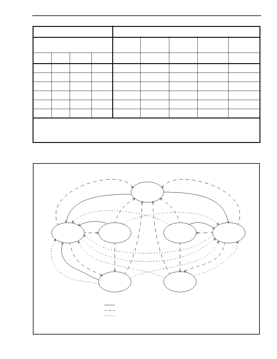
Digital Phase Lock Loop (DPLL)
As shown in Figure 4, the DPLL of the MT9044
consists of a Phase Detector, Limiter, Loop Filter,
Digitally Controlled Oscillator, and a Control Circuit.
Phase Detector - the Phase Detector compares the
virtual reference signal from the TIE Corrector circuit
with the feedback signal from the Frequency Select
MUX circuit, and provides an error signal
corresponding to the phase difference between the
two. This error signal is passed to the Limiter circuit.
The Frequency Select MUX allows the proper
feedback signal to be externally selected (e.g., 8kHz,
1.544MHz or 2.048MHz).
Limiter - the Limiter receives the error signal from
the Phase Detector and ensures that the DPLL
responds to all input transient conditions with a
maximum output phase slope of 5ns per 125us. This
is well within the maximum phase slope of 7.6ns per
125us or 81ns per 1.326ms specified by AT&T
TR62411, and Bellcore GR-1244-CORE.
Loop Filter - the Loop Filter is similar to a first order
low pass filter with a 1.9 Hz cutoff frequency for all
three reference frequency selections (8kHz,
1.544MHz or 2.048MHz). This filter ensures that the
jitter transfer requirements in ETS 300 011 and AT&T
TR62411 are met.
Control Circuit - the Control Circuit uses status and
control information from the State Machine and the
Input Impairment Circuit to set the mode of the
DPLL. The three possible modes are Normal,
Holdover and Freerun.
Digitally Controlled Oscillator (DCO) - the DCO
receives the limited and filtered signal from the Loop
FIlter, and based on its value, generates a
corresponding digital output signal. The
synchronization method of the DCO is dependent on
the state of the MT9044.
Figure 4 - DPLL Block Diagram
Limiter
Loop Filter
Digitally
Controlled
Oscillator
Phase
Detector
Feedback Signal from
Frequency Select MUX
State Select from
Input Impairment
Monitor
State Select from
State Machine
DPLL Reference to
Output Interface Circuit
Virtual Reference from
TIE Corrector
Control
Circuit
Advance Information
MT9044
7
In Normal Mode, the DCO provides an output signal
which is frequency and phase locked to the selected
input reference signal.
In Holdover Mode, the DCO is free running at a
frequency equal to the last (less 30ms to 60ms)
frequency the DCO was generating while in Normal
Mode.
In Freerun Mode, the DCO is free running with an
accuracy equal to the accuracy of the OSCi 20MHz
source.
Output Interface Circuit
The output of the DCO (DPLL) is used by the Output
Interface Circuit to provide the output signals shown
in Figure 5. The Output Interface Circuit uses four
Tapped Delay Lines followed by a T1 Divider Circuit ,
an E1 Divider Circuit, a DS2 Divider Circuit and an
analog PLL to generate the required output signals.
Four tapped delay lines are used to generate a
16.384MHz, 12.352MHz, 12.624MHz and 19.44 MHz
signals.
The E1 Divider Circuit uses the 16.384MHz signal to
generate four clock outputs and three frame pulse
outputs. The C8o, C4o and C2o clocks are
generated by simply dividing the C16o clock by two,
four and eight respectively. These outputs have a
nominal 50% duty cycle.
The T1 Divider Circuit uses the 12.384MHz signal to
generate two clock outputs. C1.5o and C3o are
generated by dividing the internal C12 clock by four
and eight respectively. These outputs have a
nominal 50% duty cycle.
The DS2 Divider Circuit uses the 12.624 MHz signal
to generate the clock output C6o. This output has a
nominal 50% duty cycle.
Figure 5 - Output Interface Circuit Block
Diagram
The frame pulse outputs (F0o, F8o, F16o, TSP, RSP)
are generated directly from the C16 clock.
The T1 and E1 signals are generated from a
common DPLL signal. Consequently, the clock
outputs C1.5o, C3o, C2o, C4o, C8o, C16o, F0o, F16o
and C6o are locked to one another for all operating
states, and are also locked to the selected input
reference in Normal Mode. See Figures 20 and 21.
All frame pulse and clock outputs have limited driving
capability, and should be buffered when driving high
capacitance (e.g. 30pF) loads.
Analog Phase Lock Loop (APLL)
The analog PLL is intended to be used to achieve a
50% duty cycle output clock. Connecting C19o to
ACKi will generate a phase locked 19.44 MHz ACKo
output with a nominal 50% duty cycle. The analog
PLL has an intrinsic jitter of less than 0.01 U.I. In
order to achieve this low jitter level a separate pin is
provided to power (AVdd) the analog PLL.
Tapped
Delay
Line
From
DPLL
T1 Divider
E1 Divider
16MHz
12MHz
C3o
C1.5o
C2o
C4o
C8o
C16o
F0o
F8o
F16o
Tapped
Delay
Line
Tapped
Delay
Line
Tapped
Delay
Line
Analog PLL
DS2 Divider
12MHz
19MHz
C6o
C19o
ACKo
ACKi
MT9044
Advance Information
8
Input Impairment Monitor
This circuit monitors the input signal to the DPLL and
automatically enables the Holdover Mode
(Auto-Holdover) when the frequency of the incoming
signal is outside the auto-holdover capture range
(See AC Electrical Characteristics - Performance).
This includes a complete loss of incoming signal, or
a large frequency shift in the incoming signal. When
the incoming signal returns to normal, the DPLL is
returned to Normal Mode with the output signal
locked to the input signal. The holdover output
signal is based on the incoming signal 30ms
minimum to 60ms prior to entering the Holdover
Mode. The amount of phase drift while in holdover is
negligible because the Holdover Mode is very
accurate (e.g.
±
0.05ppm). The the Auto-Holdover
circuit does not use TIE correction. Consequently,
the phase delay between the input and output after
switching back to Normal Mode is preserved (is the
same as just prior to the switch to Auto-Holdover).
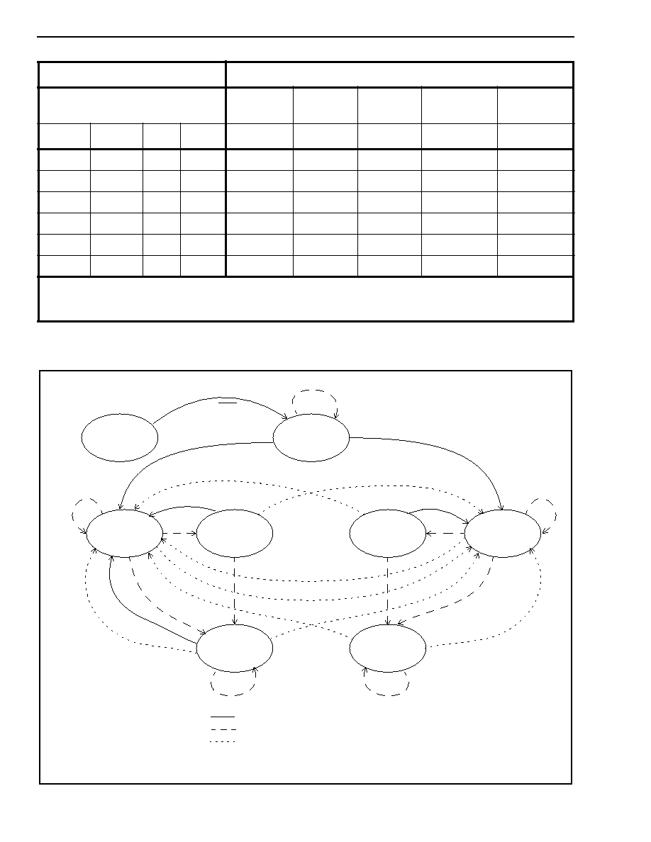
Automatic/Manual Control State Machine
The Automatic/Manual Control State Machine allows
the MT9044 to be controlled automatically (i.e.
LOS1, LOS2 and GTi signals) or controlled manually
(i.e. MS1, MS2, GTi and RSEL signals). With
manual control a single mode of operation (i.e.
Normal, Holdover and Freerun) is selected. Under
automatic control the state of the LOS1, LOS2 and
GTi signals determines the sequence of modes that
the MT9044 will follow.
As shown in Figure 1, this state machine controls the
Reference Select MUX, the TIE Corrector Circuit, the
DPLL and the Guard Time Circuit. Control is based
on the logic levels at the control inputs LOS1, LOS2,
RSEL, MS1, MS2 and GTi of the Guard Time Circuit
(See Figure 6).
All state machine changes occur synchronously on
the rising edge of F8o. See the Controls and Modes
of Operation section for full details on Automatic
Control and Manual Control.
Figure 6 - Automatic/Manual Control State
Machine Block Diagram
Guard Time Circuit
The GTi pin is used by the Automatic/Manual Control
State Machine in the MT9044 under either Manual or
Automatic control. The logic level at the GTi pin
performs two functions, it enables and disables the
TIE Corrector Circuit (Manual and Automatic), and it
selects which mode change takes place (Automatic
only). See the Applications - Guard Time section.
For both Manual and Automatic control, when
switching from Primary Holdover to Primary Normal,
the TIE Corrector Circuit is enabled when GTi=1, and
disabled when GTi=0.
Under Automatic control and in Primary Normal
Mode, two state changes are possible (not counting
Auto-Holdover). These are state changes to Primary
Holdover or to Secondary Normal. The logic level at
the GTi pin determines which state change occurs.
When GTi=0, the state change is to Primary
Holdover. When GTi=1, the state change is to
Secondary Normal.
Master Clock
The MT9044 can use either a clock or crystal as the
master timing source. For recommended master
timing circuits, see the Applications - Master Clock
section.
Control and Modes of Operation
The MT9044 can operate either in Manual or
Automatic Control. Each control method has three
possible modes of operation, Normal, Holdover and
Freerun.
As shown in Table 3, Mode/Control Select pins MS2
and MS1 select the mode and method of control.
MS1
MS2
To
Reference
Select MUX
To TIE
Corrector
Enable
Automatic/Manual Control
State Machine
To DPLL
State
Select
RSEL
LOS1
LOS2
To and From
Guard Time
Circuit
Control
RSEL
Input Reference
MANUAL
0
PRI
1
SEC
AUTO
0
State Machine Control
1
Reserved
Table 2 - Input Reference Selection

Advance Information
MT9044
9
Manual Control
Manual Control should be used when either very
simple MT9044 control is required, or when complex
control is required which is not accommodated by
Automatic Control. For example, very simple control
could include operation in a system which only
requires Normal Mode with reference switching
using only a single input stimulus (RSEL). Very
simple control would require no external circuitry.
Complex control could include a system which
requires state changes between Normal, Holdover
and Freerun Modes based on numerous input
stimuli. Complex control would require external
circuitry, typically a microcontroller.
Under Manual Control, one of the three modes is
selected by mode/control select pins MS2 and MS1.
The active reference input (PRI or SEC) is selected
by the RSEL pin as shown in Table 2. Refer to Table
4 and Figure 7 for details of the state change
sequences.
Automatic Control
Automatic Control should be used when simple
MT9044 control is required, which is more complex
than the very simple control provide by Manual
Control with no external circuitry, but not as complex
as Manual Control with a microcontroller. For
example, simple control could include operation in a
system which can be accommodated by the
Automatic Control State Diagram shown in Figure 8.
Automatic Control is also selected by mode/control
pins MS2 and MS1. However, the mode and active
reference source is selected automatically by the
internal Automatic State Machine (See Figure 6).
The mode and reference changes are based on the
logic levels on the LOS1, LOS2 and GTi control pins.
Refer to Table 5 and Figure 8 for details of the state
change sequences.
Normal Mode
Normal Mode is typically used when a slave clock
source, synchronized to the network is required.
In Normal Mode, the MT9044 provides timing (C1.5o,
C2o, C3o, C4o, C8o, C16o, and C19) and frame
synchronization (F0o, F8o, F16o, RSP, TSP) signals,
which are synchronized to one of two reference
inputs (PRI or SEC). The input reference signal may
have a nominal frequency of 8kHz, 1.544MHz or
2.048MHz.
From a reset condition, the MT9044 will take up to 25
seconds for the output signal to be phase locked to
the selected reference.
The selection of input references is control
dependent as shown in State Tables 4 and 5. The
reference frequencies are selected by the frequency
control pins FS2 and FS1 as shown in Table 1.
Holdover Mode
Holdover Mode is typically used for short durations
(e.g. 2 seconds) while network synchronization is
temporarily disrupted.
In Holdover Mode, the MT9044 provides timing and
synchronization signals, which are not locked to an
external reference signal, but are based on storage
techniques. The storage value is determined while
the device is in Normal Mode and locked to an
external reference signal.
When in Normal Mode, and locked to the input
reference signal, a numerical value corresponding to
the MT9044 output frequency is stored alternately in
two memory locations every 30ms. When the device
is switched into Holdover Mode, the value in memory
from between 30ms and 60ms is used to set the
output frequency of the device.
The frequency accuracy of Holdover Mode is
±
0.05ppm, which translates to a worst case 35 frame
(125us) slips in 24 hours. This meets the Bellcore
GR-1244-CORE Stratum 3 requirement of
±
0.37ppm
(255 frame slips per 24 hours).
Two factors affect the accuracy of Holdover Mode.
One is drift on the Master Clock while in Holdover
Mode, drift on the Master Clock directly affects the
Holdover Mode accuracy. Note that the absolute
Master Clock (OSCi) accuracy does not affect
Holdover accuracy, only the change in OSCi
accuracy while in Holdover. For example, a
±
32ppm
MS2
MS1
Control
Mode
0
0
MANUAL
NORMAL
0
1
MANUAL
HOLDOVER
1
0
MANUAL
FREERUN
1
1
AUTO
State Machine Control
Table 3 - Operating Modes and States

MT9044
Advance Information
10
master clock may have a temperature coefficient of
±
0.1ppm per degree C. So a 10 degree change in
temperature, while the MT9044 is in Holdover Mode
may result in an additional offset (over the
±
0.05ppm) in frequency accuracy of
±
1ppm, which
is much greater than the
±
0.05ppm of the MT9044.
The other factor affecting accuracy is large jitter on
the reference input prior (30ms to 60ms) to the
mode switch. For instance, jitter of 7.5UI at 700Hz
may reduce the Holdover Mode accuracy from
0.05ppm to 0.10ppm.
Freerun Mode
Freerun Mode is typically used when a master clock
source is required, or immediately following system
power-up before network synchronization is
achieved.
In Freerun Mode, the MT9044 provides timing and
synchronization signals which are based on the
master clock frequency (OSCi) only, and are not
synchronized to the reference signals (PRI and
SEC).
The accuracy of the output clock is equal to the
accuracy of the master clock (OSCi). So if a
±
32ppm
output clock is required, the master clock must also
be
±
32ppm. See Applications - Crystal and Clock
Oscillator sections.
Advance Information
MT9044
11
Figure 7 - Manual Control State Diagram
Description
State
Input Controls
Freerun
Normal
(PRI)
Normal
(SEC)
Holdover
(PRI)
Holdover
(SEC)
MS2
MS1
RSEL
GTi
S0
S1
S2
S1H
S2H
0
0
0
0
S1
-
S1 MTIE
S1
S1 MTIE
0
0
0
1
S1
-
S1 MTIE
S1 MTIE
S1 MTIE
0
0
1
X
S2
S2 MTIE
-
S2 MTIE
S2 MTIE
0
1
0
X
/
S1H
/
-
/
0
1
1
X
/
S2H
S2H
/
-
1
0
X
X
-
S0
S0
S0
S0
Legend:
- No Change
/ Not Valid
MTIE State change occurs with TIE Corrector Circuit
Refer to Manual Control State Diagram for state changes to and from Auto-Holdover State
Table 4 - Manual Control State Table
Phase Re-Alignment
Phase Continuity Maintained (without TIE Corrector Circuit)
Phase Continuity Maintained (with TIE Corrector Circuit)
NOTES:
(XXX)
MS2 MS1 RSEL
{A}
Invalid Reference Signal
Movement to Normal State from any
state requires a valid input signal
{A}
{A}
S0
Freerun
(10X)
S2H
Holdover
Secondary
(011)
S1H
Holdover
Primary
(010)
S2
Normal
Secondary
(001)
S1
Normal
Primary
(000)
(GTi=0)
(GTi=1)
S1A
Auto-Holdover
Primary
(000)
S2A
Auto-Holdover
Secondary
(001)
MT9044
Advance Information
12
Figure 8 - Automatic Control State Diagram
Description
State
Input Controls
Freerun
Normal
(PRI)
Normal
(SEC)
Holdover
(PRI)
Holdover
(SEC)
LOS2
LOS1
GTi
RST
S0
S1
S2
S1H
S2H
1
1
X
0 to 1
-
S0
S0
S0
S0
X
0
0
1
S1
-
S1 MTIE
S1
S1 MTIE
X
0
1
1
S1
-
S1 MTIE
S1 MTIE
S1 MTIE
0
1
0
1
S1
S1H
-
-
S2 MTIE
0
1
1
1
S2
S2 MTIE
-
S2 MTIE
S2 MTIE
1
1
X
1
-
S1H
S2H
-
-
Legend:
- No Change
MTIE State change occurs with TIE Corrector Circuit
Refer to Automatic Control State Diagram for state changes to and from Auto-Holdover State
Table 5 - Automatic Control (MS1=MS2=1, RSEL=0) State Table
(01X)
(X0X)
(01X)
(X0X)
{A}
(11X)
(011)
(11X)
(011)
(X0X)
(11X)
(01X)
(01X)
(010 or 11X)
(X0X)
(X0X)
(01X)
(X01)
Reset
{A}
S0
Freerun
S2H
Holdover
Secondary
S1H
Holdover
Primary
S2
Normal
Secondary
S1
Normal
Primary
(X00)
S1A
Auto-Holdover
Primary
S2A
Auto-Holdover
Secondary
(010 or 11X)
(11X) RST=1
(X0X)
NOTES:
(XXX)
LOS2 LOS1 GTi
{A}
Invalid Reference Signal
Movement to Normal State from any
state requires a valid input signal
Phase Re-Alignment
Phase Continuity Maintained (without TIE Corrector Circuit)
Phase Continuity Maintained (with TIE Corrector Circuit)

Advance Information
MT9044
13
MT9044 Measures of Performance
The following are some synchronizer performance
indicators and their corresponding definitions.
Intrinsic Jitter
Intrinsic jitter is the jitter produced by the
synchronizing circuit and is measured at its output.
It is measured by applying a reference signal with no
jitter to the input of the device, and measuring its
output jitter. Intrinsic jitter may also be measured
when the device is in a non-synchronizing mode,
such as free running or holdover, by measuring the
output jitter of the device. Intrinsic jitter is usually
measured with various bandlimiting filters depending
on the applicable standards.
Jitter Tolerance
Jitter tolerance is a measure of the ability of a PLL to
operate properly (i.e., remain in lock and or regain
lock in the presence of large jitter magnitudes at
various jitter frequencies) when jitter is applied to its
reference. The applied jitter magnitude and jitter
frequency depends on the applicable standards.
Jitter Transfer
Jitter transfer or jitter attenuation refers to the
magnitude of jitter at the output of a device for a
given amount of jitter at the input of the device. Input
jitter is applied at various amplitudes and
frequencies, and output jitter is measured with
various filters depending on the applicable
standards.
For the MT9044, two internal elements determine
the jitter attenuation. This includes the internal
1.9Hz low pass loop filter and the phase slope
limiter. The phase slope limiter limits the output
phase slope to 5ns/125us. Therefore, if the input
signal exceeds this rate, such as for very large
amplitude low frequency input jitter, the maximum
output phase slope will be limited (i.e. attenuated) to
5ns/125us.
The MT9044 has thirteen outputs with three possible
input frequencies for a total of 39 possible jitter
transfer functions. However, the data sheet section
on AC Electrical Characteristics - Jitter Transfer
specifies transfer values for only three cases, 8kHz
to 8kHz, 1.544MHz to 1.544MHz and 2.048MHz to
2.048MHz. Since all outputs are derived from the
same signal, these transfer values apply to all
outputs.
It should be noted that 1UI at 1.544MHz is 644ns,
which is not equal to 1UI at 2.048MHz, which is
488ns. Consequently, a transfer value using
different input and output frequencies must be
calculated in common units (e.g. seconds) as shown
in the following example.
What is the T1 and E1 output jitter when the T1 input
jitter is 20UI (T1 UI Units) and the T1 to T1 jitter
attenuation is 18dB?
Using the above method, the jitter attenuation can be
calculated for all combinations of inputs and outputs
based on the three jitter transfer functions provided.
Note that the resulting jitter transfer functions for all
combinations of inputs (8kHz, 1.544MHz, 2.048MHz)
and outputs (8kHz, 1.544MHz, 2.048MHz,
4.096MHz, 8.192MHz, 16.384MHz) for a given input
signal (jitter frequency and jitter amplitude) are the
same.
Since intrinsic jitter is always present, jitter
attenuation will appear to be lower for small input
jitter signals than for large ones. Consequently,
accurate jitter transfer function measurements are
usually made with large input jitter signals (e.g. 75%
of the specified maximum jitter tolerance).
Frequency Accuracy
Frequency accuracy is defined as the absolute
tolerance of an output clock signal when it is not
locked to an external reference, but is operating in a
free running mode. For the MT9044, the Freerun
accuracy is equal to the Master Clock (OSCi)
accuracy.
Holdover Accuracy
Holdover accuracy is defined as the absolute
tolerance of an output clock signal, when it is not
OutputT 1
InputT 1
A
≠
20
-------
◊
10
=
OutputT 1
20
18
≠
20
---------
◊
10
2.5UI T 1
(
)
=
=
OutputE1
OutputT 1
644ns
(
)
488ns
(
)
-------------------
3.3UI T 1
(
)
=
◊
=
OutputE1
OutputT 1
1UIT 1
(
)
1UIE1
(
)
----------------------
◊
=

MT9044
Advance Information
14
locked to an external reference signal, but is
operating using storage techniques. For the
MT9044, the storage value is determined while the
device is in Normal Mode and locked to an external
reference signal.
The absolute Master Clock (OSCi) accuracy of the
MT9044 does not affect Holdover accuracy, but the
change in OSCi accuracy while in Holdover Mode
does.
Capture Range
Also referred to as pull-in range. This is the input
frequency range over which the synchronizer must
be able to pull into synchronization. The MT9044
capture range is equal to
±
230ppm minus the
accuracy of the master clock (OSCi). For example, a
±
32ppm master clock results in a capture range of
±
198ppm.
Lock Range
This is the input frequency range over which the
synchronizer must be able to maintain
synchronization. The lock range is equal to the
capture range for the MT9044.
Phase Slope
Phase slope is measured in seconds per second and
is the rate at which a given signal changes phase
with respect to an ideal signal. The given signal is
typically the output signal. The ideal signal is of
constant frequency and is nominally equal to the
value of the final output signal or final input signal.
Time Interval Error (TIE)
TIE is the time delay between a given timing signal
and an ideal timing signal.
Maximum Time Interval Error (MTIE)
MTIE is the maximum peak to peak delay between a
given timing signal and an ideal timing signal within a
particular observation period.
Phase Continuity
Phase continuity is the phase difference between a
given timing signal and an ideal timing signal at the
end of a particular observation period. Usually, the
given timing signal and the ideal timing signal are of
the same frequency. Phase continuity applies to the
output of the synchronizer after a signal disturbance
due to a reference switch or a mode change. The
observation period is usually the time from the
disturbance, to just after the synchronizer has settled
to a steady state.
In the case of the MT9044, the output signal phase
continuity is maintained to within
±
5ns at the
instance (over one frame) of all reference switches
and all mode changes. The total phase shift,
depending on the switch or type of mode change,
may accumulate up to
±
200ns over many frames.
The rate of change of the
±
200ns phase shift is
limited to a maximum phase slope of approximately
5ns/125us. This meets the maximum phase slope
requirement of Bellcore GR-1244-CORE (81ns/
1.326ms).
Phase Lock Time
This is the time it takes the synchronizer to phase
lock to the input signal. Phase lock occurs when the
input signal and output signal are not changing in
phase with respect to each other (not including jitter).
Lock time is very difficult to determine because it is
affected by many factors which include:
i) initial input to output phase difference
ii) initial input to output frequency difference
iii) synchronizer loop filter
iv) synchronizer limiter
Although a short lock time is desirable, it is not
always possible to achieve due to other synchronizer
requirements. For instance, better jitter transfer
performance is achieved with a lower frequency loop
filter which increases lock time. And better (smaller)
phase slope performance (limiter) results in longer
lock times. The MT9044 loop filter and limiter were
optimized to meet the AT&T TR62411 jitter transfer
and phase slope requirements. Consequently,
phase lock time, which is not a standards
requirement, may be longer than in other
applications. See AC Electrical Characteristics -
Performance for maximum phase lock time.
MTIE S
( )
TIEmax t
( )
TIEmin t
( )
≠
=
Advance Information
MT9044
15
MT9044 and Network Specifications
The MT9044 fully meets all applicable PLL
requirements (intrinsic jitter/wander, jitter/wander
tolerance, jitter/wander transfer, frequency accuracy,
frequency holdover accuracy, capture range, phase
change slope and MTIE during reference
rearrangement) for the following specifications.
1. Bellcore GR-1244-CORE June 1995 for
Stratum 3, Stratum 4 Enhanced and Stratum 4
2. AT&T TR62411 (DS1) December 1990 for
Stratum 3, Stratum 4 Enhanced and Stratum 4
3. ANSI T1.101 (DS1) February 1994 for
Stratum 3, Stratum 4 Enhanced and Stratum 4
4. ETSI 300 011 (E1) April 1992 for
Single Access and Multi Access
5. TBR 4 November 1995
6. TBR 12 December 1993
7. TBR 13 January 1996
8. ITU-T I.431 March 1993
9. ITU-T G.812 June 1998 for type IV clocks for
1,544 kbit/s interfaces and 2,048 kbit/s interfaces
Applications
This section contains MT9044 application specific
details for clock and crystal operation, guard time
usage, reset operation, power supply decoupling,
Manual Control operation and Automatic Control
operation.
Master Clock
The MT9044 can use either a clock or crystal as the
master timing source.
In Freerun Mode, the frequency tolerance at the
clock outputs is identical to the frequency tolerance
of the source at the OSCi pin. For applications not
requiring an accurate Freerun Mode, tolerance of the
master timing source may be
±
100ppm. For
applications requiring an accurate Freerun Mode,
such as Bellcore GR-1244-CORE, the tolerance of
the master timing source must Be no greater than
±
32ppm.
Another consideration in determining the accuracy of
the master timing source is the desired capture
range. The sum of the accuracy of the master timing
source and the capture range of the MT9044 will
always equal
±
230ppm. For example, if the master
timing source is
±
100ppm, then the capture range
will be
±
130ppm.
Clock Oscillator - when selecting a Clock Oscillator,
numerous parameters must be considered. This
includes absolute frequency, frequency change over
temperature, output rise and fall times, output levels
and duty cycle. See AC Electrical Characteristics.
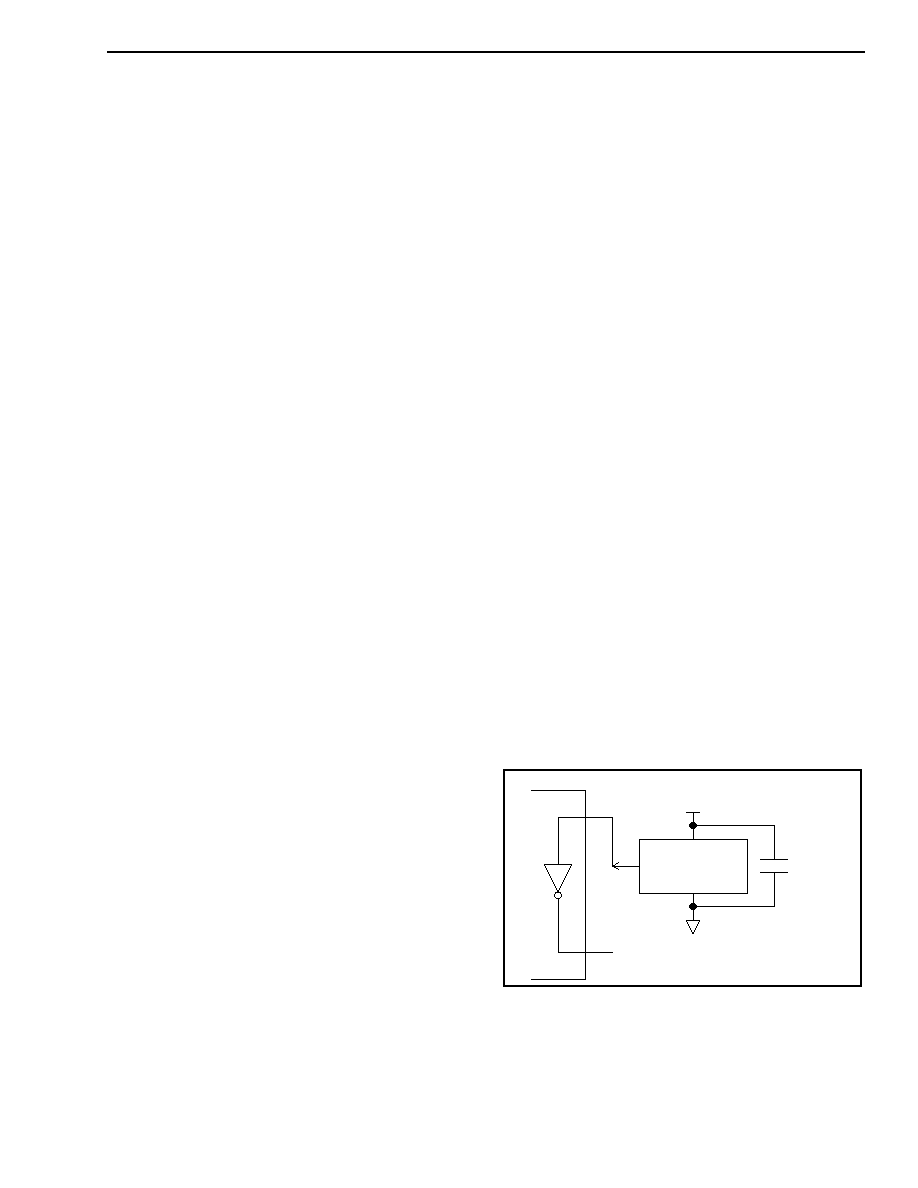
Figure 9 - Clock Oscillator Circuit
For applications requiring
±
32ppm clock accuracy,
the following clock oscillator module may be used.
CTS CXO-65-HG-5-C-20.0MHz
Frequency:
20MHz
Tolerance:
25ppm 0C to 70C
+5V
20MHz OUT
GND
0.1uF
+5V
OSCo
MT9044
OSCi
No Connection
MT9044
Advance Information
16
Rise & Fall Time:
8ns (0.5V 4.5V 50pF)
Duty Cycle:
45% to 55%
The output clock should be connected directly (not
AC coupled) to the OSCi input of the MT9044, and
the OSCo output should be left open as shown in
Figure 9.
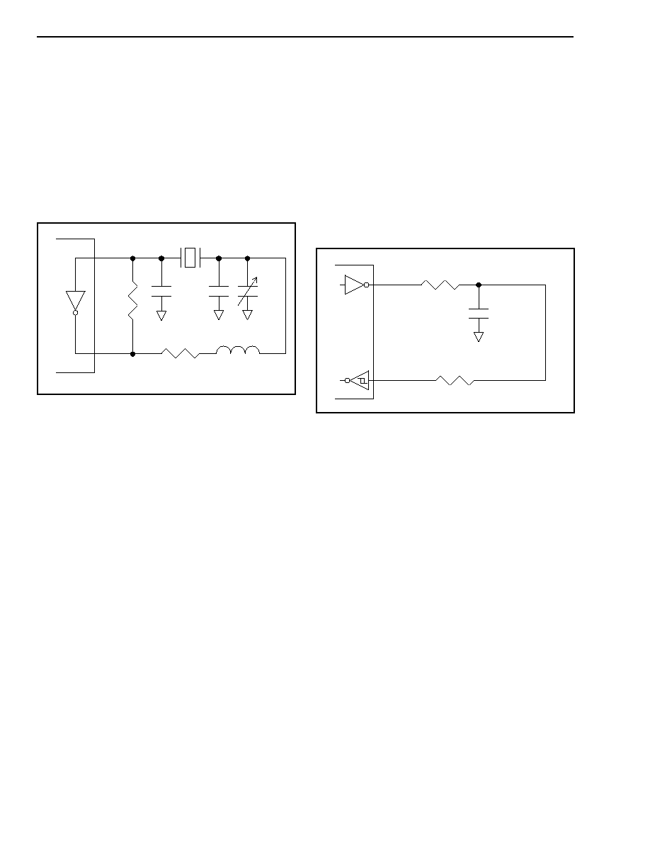
Crystal Oscillator - Alternatively, a Crystal
Oscillator may be used. A complete oscillator circuit
made up of a crystal, resistor and capacitors is
shown in Figure 10.
Figure 10 - Crystal Oscillator Circuit
The accuracy of a crystal oscillator depends on the
crystal tolerance as well as the load capacitance
tolerance. Typically, for a 20MHz crystal specified
with a 32pF load capacitance, each 1pF change in
load capacitance contributes approximately 9ppm to
the frequency deviation. Consequently, capacitor
tolerances, and stray capacitances have a major
effect on the accuracy of the oscillator frequency.
The trimmer capacitor shown in Figure 10 may be
used to compensate for capacitive effects. If
accuracy is not a concern, then the trimmer may be
removed, the 39pF capacitor may be increased to
56pF, and a wider tolerance crystal may be
substituted.
The crystal should be a fundamental mode type - not
an overtone. The fundamental mode crystal permits
a simpler oscillator circuit with no additional filter
components and is less likely to generate spurious
responses. The crystal specification is as follows.
Frequency:
20MHz
Tolerance:
As required
Oscillation Mode:
Fundamental
Resonance Mode:
Parallel
Load Capacitance:
32pF
Maximum Series Resistance:
35
Approximate Drive Level:
1mW
e.g., CTS R1027-2BB-20.0MHZ
(
±
20ppm absolute,
±
6ppm 0C to 50C, 32pF, 25
)
Guard Time Adjustment
Excessive switching of the timing reference (from
PRI to SEC) in the MT9044 can be minimized by first
entering Holdover Mode for a predetermined
maximum time (i.e., guard time). If the degraded
signal returns to normal before the expiry of the
guard time (e.g. 2.5 seconds), then the MT9044 is
returned to its Normal Mode (with no reference
switch taking place). Otherwise, the reference input
may be changed from Primary to Secondary.
Figure 11 - Symmetrical Guard Time Circuit
A simple way to control the guard time (using
Automatic Control) is with an RC circuit as shown in
Figure 11. Resistor R
P
is for protection only and
limits the current flowing into the GTi pin during
power down conditions. The guard time can be
calculated as follows.
∑
V
SIH
is the logic high going threshold level for the
GTi Schmitt Trigger input, see DC Electrical
Characteristics
In cases where fast toggling might be expected of
the LOS1 input, then an unsymmetrical Guard Time
Circuit is recommended. This ensures that reference
switching doesn't occur until the full guard time value
has expired. An unsymmetrical Guard Time Circuit
is shown in Figure 12.
OSCo
56pF
1M
39pF
3-50pF
20MHz
MT9044
OSCi
100
1uH
1uH inductor: may improve stability and is optional
GTi
C
10uF
R
150k
MT9044
GTo
+
R
P
1k
guard
time
RC
V
DD
V
DD
V
SIH
≠
----------------------------------
ln
◊
=
guard
time
RC
0.6
◊
guard
time
150k
10u
◊
0.6
0.9s
=
◊
example
Advance Information
MT9044
17
Figure 12 - Unsymmetrical Guard Time
Circuit
Figure 13 shows a typical timing example of an
unsymmetrical Guard Time Circuit with the MT9044
in Automatic Control.
TIE Correction (using GTi)
When Primary Holdover Mode is entered for short
time periods, TIE correction should not be enabled.
This will prevent unwanted accumulated phase
change between the input and output. This is mainly
applicable to Manual Control, since Automatic
Control together with the Guard Time Circuit
inherently operate in this manner.
For instance, 10 Normal to Holdover to Normal mode
change sequences occur, and in each case Holdover
was entered for 2s. Each mode change sequence
could account for a phase change as large as 350ns.
Thus, the accumulated phase change could be as
large as 3.5us, and, the overall MTIE could be as
large as 3.5us.
∑
0.05ppm is the accuracy of Holdover Mode
∑
50ns is the maximum phase continuity of the
MT9044 from Normal Mode to Holdover Mode
∑
200ns is the maximum phase continuity of the
MT9044 from Holdover Mode to Normal Mode (with
or without TIE Corrector Circuit)
When 10 Normal to Holdover to Normal mode
change sequences occur without MTIE enabled, and
in each case holdover was entered for 2s, each
mode change sequence could still account for a
phase change as large as 350ns. However, there
would be no accumulated phase change, since the
input to output phase is re-aligned after every
Holdover to Normal state change. The overall MTIE
would only be 350ns.
R
P
1k
GTi
C
10uF
R
C
150k
MT9044
GTo
+
R
D
1k
Phase
hold
0.05 ppm
2s
◊
100ns
=
=
Phase
state
50ns
200ns
250ns
=
+
=
Phase
10
10
250ns
100ns
+
(
)
◊
3.5us
=
=
Figure 13 - Automatic Control, Unsymmetrical Guard Time Circuit Timing Example
PRI
NORMAL
SEC
NORMAL
PRI
HOLDOVER
PRI
NORMAL
LOS2
GOOD
PRI
SIGNAL
STATUS
SEC
SIGNAL
STATUS
LOS1
PRI
NORMAL
PRI
HOLDOVER
BAD
GOOD
BAD
GOOD
GOOD
GTo
GTi
MT9044
STATE
V
SIH
NOTES:
1. T
D
represents the time delay from when the reference goes
bad to when the MT9044 is provided with a LOS indication.
T
D
T
D

18
MT9044
Advance Information
Reset Circuit
A simple power up reset circuit with about a 50us
reset low time is shown in Figure 14. Resistor R
P
is
for protection only and limits current into the RST pin
during power down conditions. The reset low time is
not critical but should be greater than 300ns.
Figure 14 - Power-Up Reset Circuit
Dual T1 Reference Sources with MT9044 in
Automatic Control
For systems requiring simple state machine control,
the application circuit shown in Figure 15 using
Automatic Control may be used.
In this circuit, the MT9044 is operating Automatically,
using a Guard Time Circuit, and the LOS1 and LOS2
inputs to determine all mode changes. Since the
Guard Time Circuit is set to about 1s, all line
interruptions (LOS1=1) less than 1s will cause the
MT9044 to go from Primary Normal Mode to
Holdover Mode and not switch references. For line
interruptions greater than 1s, the MT9044 will switch
Modes from Holdover to Secondary Normal,
provided that the secondary signal is valid (LOS2=0).
After receiving a good primary signal (LOS1=0), the
MT9044 will switch back to Primary Normal Mode
For complete Automatic Control state machine
details, refer to Table 5 for the State Table, and
Figure 8 for the State Diagram.
+5V
RST
R
P
1k
C
10nF
R
10k
MT9044
Figure 15 - Dual T1 Reference Sources with MT9044 in 1.544MHz Automatic Control
1k
1k
10nF
To
TX Line
XFMR
MT8985
STo0
STi0
STo1
STi1
F0i
C4i
MT9044
F0o
C4o
FS1
GTo
FS2
GTi
PRI
SEC
LOS1
LOS2
OSCi
MS1
MS2
RSEL
To
RX Line
XFMR
To Line 1
Out
MT9074
To
TX Line
XFMR
DSTo
DSTi
F0i
C4i
TTIP
TRING
RTIP
RRING
LOS
E1.5o
To
RX Line
XFMR
To Line 2
10uF
150k
RST
TRST
10k
+
MT9074
DSTo
DSTi
F0i
C4i
TTIP
TRING
RTIP
RRING
LOS
E1.5o
20MHz
±
32ppm
CLOCK
1k
+ 5V
+ 5V
+ 5V
Advance Information
MT9044
19
Dual E1 Reference Sources with MT9044 in
Manual Control
For systems requiring complex state machine
control, the application circuit shown in Figure 16
using Manual Control may be used.
In this circuit, the MT9044 is operating Manually
and is using a controller for all mode changes. The
controller sets the MT9044 modes (Normal, Holdover
or Freerun) by controlling the MT9044 mode/control
select pins (MS2 and MS1). The input (Primary or
Secondary) is selected with the reference select pin
(RSEL). TIE correction from Primary Holdover Mode
to Primary Normal Mode is enabled and disabled
with the guard time input pin (GTi). The input to
output phase alignment is re-aligned with the TIE
circuit reset pin (TCLR), and a complete device reset
is done with the RST pin.
The controller uses two stimulus inputs (LOS)
directly from the MT9075 E1 interfaces, as well as an
external stimulus input. The external input may
come from a device that monitors the status registers
of the E1 interfaces, and outputs a logic one in the
event of an unacceptable status condition.
For complete Manual Control state machine details,
refer to Table 4 for the State Table, and Figure 7 for
the State Diagram.
Figure 16 - Dual E1 Reference Sources with MT9044 in 8kHz Manual Control
CONTROLLER
To
TX Line
XFMR
MT8985
STo0
STi0
STo1
STi1
F0i
C4i
MT9044
F0o
C4o
C1.5o
FS1
FS2
GTi
PRI
SEC
LOS1
LOS2
OSCi
MS1
MS2
RSEL
To
RX Line
XFMR
To Line 1
To
TX Line
XFMR
To
RX Line
XFMR
To Line 2
RST
TRST
MT9075
DSTo
DSTi
F0i
C4i
RxFP
TTIP
TRING
RTIP
RRING
LOS
External Stimulus
MT9075
DSTo
DSTi
F0i
C4i
RxFP
TTIP
TRING
RTIP
RRING
LOS
Out
20MHz
±
32ppm
CLOCK
+ 5V
MT9044
Advance Information
20
Single Reference Source E1 to STS-3 with 8 kHz
Reference
The device may operate in freerun mode or with a
single reference source. The 8 kHz output from the
MT9075 is sourced from the clock extracted from the
E1 trunk. It becomes the reference for the PLL which
then generates ST-BUS signals F0o, C4o and C2o to
form the system backplane clock. The MT90840
connects to the system backplane, as well as to an
OC3 link via an STS-3 Framer and optical link. The
19.44 Mhz clock required by the MT90840 is
generated by the MT9044. In the event that the E1
link is broken, the LOS output of the MT9075 goes
high placing the MT9044 in freerun mode.
Figure 17 - Single Source - E1 to STS-3 with 8kHz Reference
To
TX Line
XFMR
MT90820
STo0
STi0
STo1-8
STi1-8
F0i
C4i
MT9044
F0o
C4o
C1.5o
FS1
FS2
GTi
PRI
LOS1
LOS2
OSCi
MS1
MS2
RSEL
To
RX Line
XFMR
To E1 Line
To
TX Line
XFMR
To
RX Line
XFMR
To OC3 Line
RST
TCLR
MT9075
DSTo
DSTi
F0i
C4i
RxFP
TTIP
TRING
RTIP
RRING
LOS
MT90840
STo0-7
STi0-7
F0i
C4b
PDo0-7
PDi0-7
PCKR
Out
20MHz
±
32ppm
CLOCK
+ 5V
PCKT
PPFRi
C19o
1k
10nF
10k
+ 5V
PPFTo
ACKi
ACKo
Advance Information
MT9044
21
* Exceeding these values may cause permanent damage. Functional operation under these conditions is not implied.
* Supply voltage and operating temperature are as per Recommended Operating Conditions.
Absolute Maximum Ratings* -
Voltages are with respect to ground (V
SS
) unless otherwise stated.
Parameter
Symbol
Min
Max
Units
1
Supply voltage
V
DD
-0.3
7.0
V
2
Voltage on any pin
V
PIN
-0.3
V
DD
+0.3
V
3
Current on any pin
I
PIN
20
mA
4
Storage temperature
T
ST
-55
125
∞
C
5
PLCC package power dissipation
P
PD
900
mW
6
MQFP package power dissipation
P
PD
900
mW
Recommended Operating Conditions* -
* Voltages are with respect to ground (V
SS
) unless otherwise stated.
Characteristics
Sym
Min
Max
Units
1
Supply voltage
V
DD
4.5
5.5
V
2
Operating temperature
T
A
-40
85
C
DC Electrical Characteristics* -
* Voltages are with respect to ground (V
SS
) unless otherwise stated.
Characteristics
Sym
Min
Max
Units
Conditions/Notes
1
Supply current with: OSCi = 0V
I
DDS
10
mA
Outputs unloaded
2
OSCi = Clock
I
DD
90
mA
Outputs unloaded
3
TTL high-level input voltage
V
IH
2.0
V
4
TTL low-level input voltage
V
IL
0.8
V
5
CMOS high-level input voltage
V
CIH
0.7V
DD
V
OSCi
6
CMOS low-level input voltage
V
CIL
0.3V
DD
V
OSCi
7
Schmitt high-level input voltage
V
SIH
2.3
V
GTi, RST
8
Schmitt low-level input voltage
V
SIL
0.8
V
GTi, RST
9
Schmitt hysteresis voltage
V
HYS
0.4
V
GTi, RST
10
Input leakage current
I
IL
-10
+10
u
A
V
I
=V
DD
or 0V
11
High-level output voltage
V
OH
0.8V
DD
V
I
OH
=4mA
12
Low-level output voltage
V
OL
0.2V
DD
V
I
OL
=4mA
MT9044
Advance Information
22
See "Notes" following AC Electrical Characteristics tables.
* Supply voltage and operating temperature are as per Recommended Operating Conditions.
* Timing for input and output signals is based on the worst case result of the combination of TTL and CMOS thresholds.
* See Figure 18.
Figure 18 - Timing Parameter Measurement Voltage Levels
AC Electrical Characteristics - Performance
Characteristics
Sym
Min
Max
Units
Conditions/Notes
1
Freerun Mode accuracy with OSCi at:
±±
0ppm
-0
+0
ppm
5-8
2
±
32ppm
-32
+32
ppm
5-8
3
±
100ppm
-100
+100
ppm
5-8
4
Holdover Mode accuracy with OSCi at:
±
0ppm
-0.05
+0.05
ppm
1,2,4,6-8,40
5
±
32ppm
-0.05
+0.05
ppm
1,2,4,6-8,40
6
±
100ppm
-0.05
+0.05
ppm
1,2,4,6-8,40
7
Capture range with OSCi at:
±
0ppm
-230
+230
ppm
1-3,6-8
8
±
32ppm
-198
+198
ppm
1-3,6-8
9
±
100ppm
-130
+130
ppm
1-3,6-8
10
Phase lock time
30
s
1-3,6-14
11
Output phase continuity with: reference switch
200
ns
1-3,6-14
12
mode switch to Normal
200
ns
1-2,4-14
13
mode switch to Freerun
200
ns
1-,4,6-14
14
mode switch to Holdover
50
ns
1-3,6-14
15
MTIE (maximum time interval error)
600
ns
1-14,27
16
Output phase slope
45
us/s
1-14,27
17
Reference input for Auto-Holdover with: 8kHz
-18k
+18k
ppm
1-3,6,9-11
18
1.544MHz
-36k
+36k
ppm
1-3,7,9-11
19
2.048MHz
-36k
+36k
ppm
1-3,8-11
AC Electrical Characteristics - Timing Parameter Measurement Voltage Levels* -
Voltages are
with respect to ground (V
SS
) unless otherwise stated.
Characteristics
Sym
Schmitt
TTL
CMOS
Units
1
Threshold Voltage
V
T
1.5
1.5
0.5V
DD
V
2
Rise and Fall Threshold Voltage High
V
HM
2.3
2.0
0.7V
DD
V
3
Rise and Fall Threshold Voltage Low
V
LM
0.8
0.8
0.3V
DD
V
t
IRF,
t
ORF
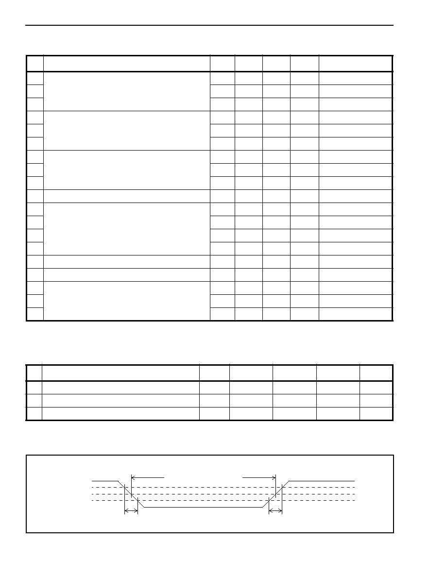
Timing Reference Points
ALL SIGNALS
V
HM
V
T
V
LM
t
IRF,
t
ORF
Advance Information
MT9044
23
See "Notes" following AC Electrical Characteristics tables.
AC Electrical Characteristics - Input/Output Timing
Characteristics
Sym
Min
Max
Units
1
Reference input pulse width high or low
t
RW
100
ns
2
Reference input rise or fall time
t
IRF
10
ns
3
8kHz reference input to F8o delay
t
R8D
-21
6
ns
4
1.544MHz reference input to F8o delay
t
R15D
337
363
ns
5
2.048MHz reference input to F8o delay
t
R2D
222
238
ns
6
F8o to F0o delay
t
F0D
110
134
ns
7
F16o setup to C16o falling
t
F16S
11
35
ns
8
F16o hold from C16o rising
t
F16H
0
20
ns
9
F8o to C1.5o delay
t
C15D
-51
-37
ns
10
F8o to C6o delay
t
C6D
-3
11
ns
11
F8o to C3o delay
t
C3D
-51
-37
ns
12
F8o to C2o delay
t
C2D
-13
2
ns
13
F8o to C4o delay
t
C4D
-13
2
ns
14
F8o to C8o delay
t
C8D
-13
2
ns
15
F8o to C16o delay
t
C16D
-13
2
ns
16
F8o to TSP delay
t
TSPD
-10
10
ns
17
F8o to RSP delay
t
RSPD
-10
10
ns
18
F8o to C19o delay
t
C19D
0
52
ns
19
C1.5o pulse width high or low
t
C15W
309
339
ns
20
C3o pulse width high or low
t
C3W
149
175
ns
21
C6o pulse width high or low
t
C6W
72
86
ns
22
C2o pulse width high or low
t
C2W
230
258
ns
23
C4o pulse width high or low
t
C4W
111
133
ns
24
C8o pulse width high or low
t
C8W
52
70
ns
25
C16o pulse width high or low
t
C16WL
24
35
ns
26
TSP pulse width high
t
TSPW
478
494
ns
27
RSP pulse width high
t
RSPW
474
491
ns
28
C19o pulse width high or low
t
C19W
16
36
ns
29
F0o pulse width low
t
F0WL
230
258
ns
30
F8o pulse width high
t
F8WH
111
133
ns
31
F16o pulse width low
t
F16WL
52
70
ns
32
Output clock and frame pulse rise or fall time
t
ORF
9
ns
33
Input Controls Setup Time
t
S
100
ns
34
Input Controls Hold Time
t
H
100
ns
MT9044
Advance Information
24
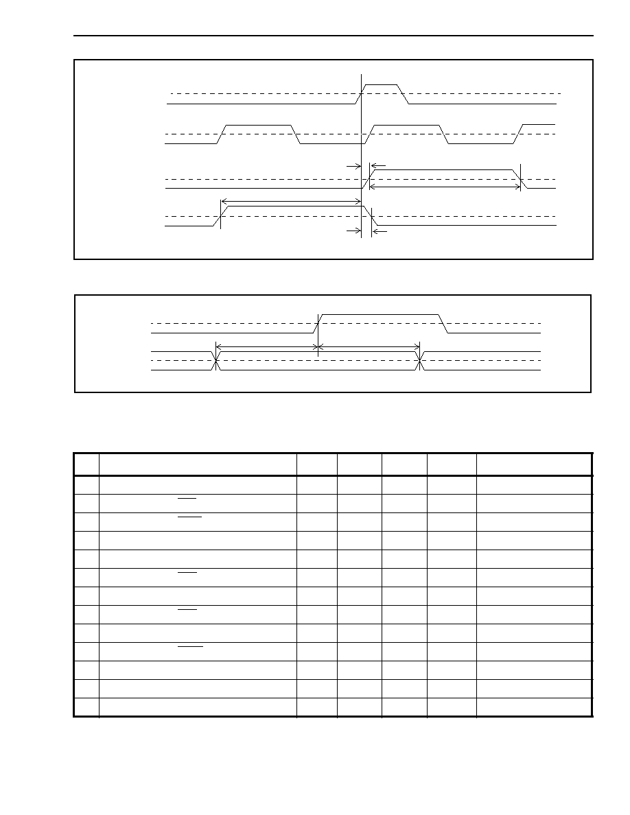
Figure 19 - Input to Output Timing (Normal Mode)
Figure 20 - Output Timing 1
t
RW
t
R15D
t
R2D
t
R8D
F8o
NOTES:
1. Input to output delay values
are valid after a TRST or RST
with no further state changes
V
T
V
T
V
T
V
T
PRI/SEC
8kHz
PRI/SEC
2.048MHz
PRI/SEC
1.544MHz
t
RW
t
RW
t
F16WL
t
F8WH
t
C15W
t
C15D
t
C3D
t
C4D
t
C16D
t
C8D
t
F16S
t
F0D
F0o
F16o
C16o
C8o
C4o
C2o
C3o
C1.5o
t
C2D
F8o
t
C4W
t
F0WL
t
C16WL
t
C8W
t
C2W
t
C3W
t
C8W
t
C4W
t
C3W
V
T
V
T
V
T
V
T
V
T
V
T
V
T
V
T
V
T
t
C19W
C19o
t
C19D
t
C6D
t
C6W
t
C6W
C6o
t
C19W
V
T
V
T
t
F16H
Advance Information
MT9044
25
Figure - 21 Output Timing 2
Figure 22 - Input Controls Setup and Hold Timing
See "Notes" following AC Electrical Characteristics tables.
AC Electrical Characteristics - Intrinsic Jitter Unfiltered
Characteristics
Sym
Min
Max
Units
Conditions/Notes
1
Intrinsic jitter at F8o (8kHz)
0.0002
UIpp
1-14,21-24,28
2
Intrinsic jitter at F0o (8kHz)
0.0002
UIpp
1-14,21-24,28
3
Intrinsic jitter at F16o (8kHz)
0.0002
UIpp
1-14,21-24,28
4
Intrinsic jitter at C1.5o (1.544MHz)
0.030
UIpp
1-14,21-24,29
5
Intrinsic jitter at C2o (2.048MHz)
0.040
UIpp
1-14,21-24,30
6
Intrinsic jitter at C3o (3.088MHz)
0.060
UIpp
1-14,21-24,31
7
Intrinsic jitter at C6o (6.312MHz)
0.120
UIpp
1-14,21-24,31
8
Intrinsic jitter at C4o (4.096MHz)
0.080
UIpp
1-14,21-24,32
9
Intrinsic jitter at C8o (8.192MHz)
0.160
UIpp
1-14,21-24,33
10
Intrinsic jitter at C16o (16.384MHz)
0.320
UIpp
1-14,21-24,34
11
Intrinsic jitter at TSP (8kHz)
0.0002
UIpp
1-14,21-24,28
12
Intrinsic jitter at RSP (8kHz)
0.0002
UIpp
1-14,21-24,28
13
Intrinsic jitter at C19o (19.44MHz)
0.10
UIpp
1-14,21-24,41
t
RSPD
t
TSPD
TSP
C2o
t
TSPW
t
RSPW
V
T
V
T
V
T
V
T
RSP
F8o
t
H
t
S
F8o
MS1,2
LOS1,2
RSEL, GTi
V
T
V
T

MT9044
Advance Information
26
See "Notes" following AC Electrical Characteristics tables.
See "Notes" following AC Electrical Characteristics tables
See "Notes" following AC Electrical Characteristics tables.
See "Notes" following AC Electrical Characteristics tables.
AC Electrical Characteristics - C1.5o (1.544MHz) Intrinsic Jitter Filtered
Characteristics
Sym
Min
Max
Units
Conditions/Notes
1
Intrinsic jitter (4Hz to 100kHz filter)
0.015
UIpp
1-14,21-24,29
2
Intrinsic jitter (10Hz to 40kHz filter)
0.010
UIpp
1-14,21-24,29
3
Intrinsic jitter (8kHz to 40kHz filter)
0.010
UIpp
1-14,21-24,29
4
Intrinsic jitter (10Hz to 8kHz filter)
0.005
UIpp
1-14,21-24,29
AC Electrical Characteristics - C2o (2.048MHz) Intrinsic Jitter Filtered
Characteristics
Sym
Min
Max
Units
Conditions/Notes
1
Intrinsic jitter (4Hz to 100kHz filter)
0.015
UIpp
1-14,21-24,30
2
Intrinsic jitter (10Hz to 40kHz filter)
0.010
UIpp
1-14,21-24,30
3
Intrinsic jitter (8kHz to 40kHz filter)
0.010
UIpp
1-14,21-24,30
4
Intrinsic jitter (10Hz to 8kHz filter)
0.005
UIpp
1-14,21-24,30
AC Electrical Characteristics - 8kHz Input to 8kHz Output Jitter Transfer
Characteristics
Sym
Min
Max
Units
Conditions/Notes
1
Jitter attenuation for 1Hz@0.01UIpp input
0
6
dB
1-3,6,9-14,21-22,24,28,35
2
Jitter attenuation for 1Hz@0.54UIpp input
6
16
dB
1-3,6,9-14,21-22,24,28,35
3
Jitter attenuation for 10Hz@0.10UIpp input
12
22
dB
1-3,6,9-14,21-22,24,28,35
4
Jitter attenuation for 60Hz@0.10UIpp input
28
38
dB
1-3,6,9-14,21-22,24,28,35
5
Jitter attenuation for 300Hz@0.10UIpp input
42
dB
1-3,6,9-14,21-22,24,28,35
6
Jitter attenuation for 3600Hz@0.005UIpp input
45
dB
1-3,6,9-14,21-22,24,28,35
AC Electrical Characteristics - 1.544MHz Input to 1.544MHz Output Jitter Transfer
Characteristics
Sym
Min
Max
Units
Conditions/Notes
1
Jitter attenuation for 1Hz@20UIpp input
0
6
dB
1-3,7,9-14,21-22,24,29,35
2
Jitter attenuation for 1Hz@104UIpp input
6
16
dB
1-3,7,9-14,21-22,24,29,35
3
Jitter attenuation for 10Hz@20UIpp input
12
22
dB
1-3,7,9-14,21-22,24,29,35
4
Jitter attenuation for 60Hz@20UIpp input
28
38
dB
1-3,7,9-14,21-22,24,29,35
5
Jitter attenuation for 300Hz@20UIpp input
42
dB
1-3,7,9-14,21-22,24,29,35
6
Jitter attenuation for 10kHz@0.3UIpp input
45
dB
1-3,7,9-14,21-22,24,29,35
7
Jitter attenuation for 100kHz@0.3UIpp input
45
dB
1-3,7,9-14,21-22,24,29,35

Advance Information
MT9044
27
See "Notes" following AC Electrical Characteristics tables.
See "Notes" following AC Electrical Characteristics tables.
AC Electrical Characteristics - 2.048MHz Input to 2.048 MHz Output Jitter Transfer
Characteristics
Sym
Min
Max
Units
Conditions/Notes
1
Jitter at output for 1Hz@3.00UIpp input
2.9
UIpp
1-3,8,9-14,21-22,24,30,35
2
with 40Hz to 100kHz filter
0.09
UIpp
1-3,8,9-14,21-22,24,30,36
3
Jitter at output for 3Hz@2.33UIpp input
1.3
UIpp
1-3,8,9-14,21-22,24,30,35
4
with 40Hz to 100kHz filter
0.10
UIpp
1-3,8,9-14,21-22,24,30,36
5
Jitter at output for 5Hz@2.07UIpp input
0.80
UIpp
1-3,8,9-14,21-22,24,30,35
6
with 40Hz to 100kHz filter
0.10
UIpp
1-3,8,9-14,21-22,24,30,36
7
Jitter at output for 10Hz@1.76UIpp input
0.40
UIpp
1-3,8,9-14,21-22,24,30,35
8
with 40Hz to 100kHz filter
0.10
UIpp
1-3,8,9-14,21-22,24,30,36
9
Jitter at output for 100Hz@1.50UIpp input
0.06
UIpp
1-3,8,9-14,21-22,24,30,35
10
with 40Hz to 100kHz filter
0.05
UIpp
1-3,8,9-14,21-22,24,30,36
11
Jitter at output for 2400Hz@1.50UIpp input
0.04
UIpp
1-3,8,9-14,21-22,24,30,35
12
with 40Hz to 100kHz filter
0.03
UIpp
1-3,8,9-14,21-22,24,30,36
13
Jitter at output for 100kHz@0.20UIpp input
0.04
UIpp
1-3,8,9-14,21-22,24,30,35
14
with 40Hz to 100kHz filter
0.02
UIpp
1-3,8,9-14,21-22,24,30,36
AC Electrical Characteristics - 8kHz Input Jitter Tolerance
Characteristics
Sym
Min
Max
Units
Conditions/Notes
1
Jitter tolerance for 1Hz input
0.80
UIpp
1-3,6,9-14,21-22,24-26,28
2
Jitter tolerance for 5Hz input
0.70
UIpp
1-3,6,9-14,21-22,24-26,28
3
Jitter tolerance for 20Hz input
0.60
UIpp
1-3,6,9-14,21-22,24-26,28
4
Jitter tolerance for 300Hz input
0.20
UIpp
1-3,6,9-14,21-22,24-26,28
5
Jitter tolerance for 400Hz input
0.15
UIpp
1-3,6,9-14,21-22,24-26,28
6
Jitter tolerance for 700Hz input
0.08
UIpp
1-3,6,9-14,21-22,24-26,28
7
Jitter tolerance for 2400Hz input
0.02
UIpp
1-3,6,9-14,21-22,24-26,28
8
Jitter tolerance for 3600Hz input
0.01
UIpp
1-3,6,9-14,21-22,24-26,28
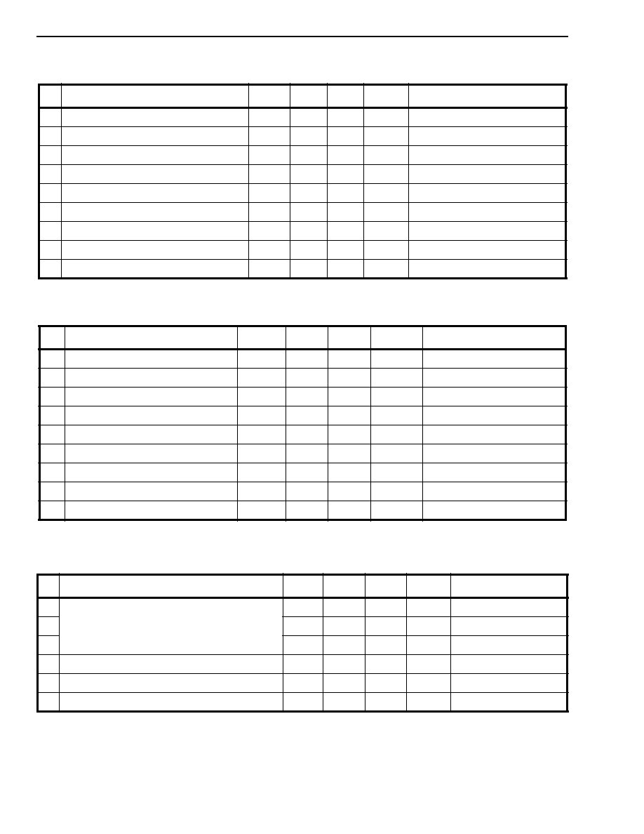
MT9044
Advance Information
28
See "Notes" following AC Electrical Characteristics tables.
See "Notes" following AC Electrical Characteristics tables.
See "Notes" following AC Electrical Characteristics tables.
AC Electrical Characteristics - 1.544MHz Input Jitter Tolerance
Characteristics
Sym
Min
Max
Units
Conditions/Notes
1
Jitter tolerance for 1Hz input
150
UIpp
1-3,7,9-14,21-22,24-26,29
2
Jitter tolerance for 5Hz input
140
UIpp
1-3,7,9-14,21-22,24-26,29
3
Jitter tolerance for 20Hz input
130
UIpp
1-3,7,9-14,21-22,24-26,29
4
Jitter tolerance for 300Hz input
35
UIpp
1-3,7,9-14,21-22,24-26,29
5
Jitter tolerance for 400Hz input
25
UIpp
1-3,7,9-14,21-22,24-26,29
6
Jitter tolerance for 700Hz input
15
UIpp
1-3,7,9-14,21-22,24-26,29
7
Jitter tolerance for 2400Hz input
4
UIpp
1-3,7,9-14,21-22,24-26,29
8
Jitter tolerance for 10kHz input
1
UIpp
1-3,7,9-14,21-22,24-26,29
9
Jitter tolerance for 100kHz input
0.5
UIpp
1-3,7,9-14,21-22,24-26,29
AC Electrical Characteristics - 2.048MHz Input Jitter Tolerance
Characteristics
Sym
Min
Max
Units
Conditions/Notes
1
Jitter tolerance for 1Hz input
150
UIpp
1-3,8,9-14,21-22,24-26,30
2
Jitter tolerance for 5Hz input
140
UIpp
1-3,8,9-14,21-22,24-26,30
3
Jitter tolerance for 20Hz input
130
UIpp
1-3,8,9-14,21-22,24-26,30
4
Jitter tolerance for 300Hz input
50
UIpp
1-3,8,9-14,21-22,24-26,30
5
Jitter tolerance for 400Hz input
40
UIpp
1-3,8,9-14,21-22,24-26,30
6
Jitter tolerance for 700Hz input
20
UIpp
1-3,8,9-14,21-22,24-26,30
7
Jitter tolerance for 2400Hz input
5
UIpp
1-3,8,9-14,21-22,24-26,30
8
Jitter tolerance for 10kHz input
1
UIpp
1-3,8,9-14,21-22,24-26,30
9
Jitter tolerance for 100kHz input
1
UIpp
1-3,8,9-14,21-22,24-26,30
AC Electrical Characteristics - OSCi 20MHz Master Clock Input
Characteristics
Sym
Min
Max
Units
Conditions/Notes
1
Frequency accuracy
(20 MHz nominal)
-0
+0
ppm
15,18
2
-32
+32
ppm
16,19
3
-100
+100
ppm
17,20
4
Duty cycle
40
60
%
5
Rise time
10
ns
6
Fall time
10
ns

Advance Information
MT9044
29
Notes:
Voltages are with respect to ground (V
SS
) unless otherwise stated.
Supply voltage and operating temperature are as per Recommended Operating Conditions.
Timing parameters are as per AC Electrical Characteristics - Timing Parameter Measurement Voltage Levels
1. PRI reference input selected.
2. SEC reference input selected.
3. Normal Mode selected.
4. Holdover Mode selected.
5. Freerun Mode selected.
6. 8kHz Frequency Mode selected.
7. 1.544MHz Frequency Mode selected.
8. 2.048MHz Frequency Mode selected.
9. Master clock input OSCi at 20MHz
±
0ppm.
10. Master clock input OSCi at 20MHz
±
32ppm.
11. Master clock input OSCi at 20MHz
±
100ppm.
12. Selected reference input at
±
0ppm.
13. Selected reference input at
±
32ppm.
14. Selected reference input at
±
100ppm.
15. For Freerun Mode of
±
0ppm.
16. For Freerun Mode of
±
32ppm.
17. For Freerun Mode of
±
100ppm.
18. For capture range of
±
230ppm.
19. For capture range of
±
198ppm.
20. For capture range of
±
130ppm.
21. 25pF capacitive load.
22. OSCi Master Clock jitter is less than 2nspp, or 0.04UIpp where1UIpp=1/20MHz.
23. Jitter on reference input is less than 7nspp.
24. Applied jitter is sinusoidal.
25. Minimum applied input jitter magnitude to regain synchronization.
26. Loss of synchronization is obtained at slightly higher input jitter amplitudes.
27. Within 10ms of the state, reference or input change.
28. 1UIpp = 125us for 8kHz signals.
29. 1UIpp = 648ns for 1.544MHz signals.
30. 1UIpp = 488ns for 2.048MHz signals.
31. 1UIpp = 323ns for 3.088MHz signals.
32. 1UIpp = 244ns for 4.096MHz signals.
33. 1UIpp = 122ns for 8.192MHz signals.
34. 1UIpp = 61ns for 16.384MHz signals.
35. No filter.
36. 40Hz to 100kHz bandpass filter.
37. With respect to reference input signal frequency.
38. After a RST or TRST.
39. Master clock duty cycle 40% to 60%.
40. Prior to Holdover Mode, device was in Normal Mode and phase locked.
41. 1Ulpp = 51ns for 19.44MHz signals.

M Mitel (design) and ST-BUS are registered trademarks of MITEL Corporation
Mitel Semiconductor is an ISO 9001 Registered Company
Copyright 1999 MITEL Corporation
All Rights Reserved
Printed in CANADA
TECHNICAL DOCUMENTATION - NOT FOR RESALE
World Headquarters - Canada
Tel: +1 (613) 592 2122
Fax: +1 (613) 592 6909
North America
Asia/Pacific
Europe, Middle East,
Tel: +1 (770) 486 0194
Tel: +65 333 6193
and Africa (EMEA)
Fax: +1 (770) 631 8213
Fax: +65 333 6192
Tel: +44 (0) 1793 518528
Fax: +44 (0) 1793 518581
http://www.mitelsemi.com
Information relating to products and services furnished herein by Mitel Corporation or its subsidiaries (collectively "Mitel") is believed to be reliable. However, Mitel assumes no
liability for errors that may appear in this publication, or for liability otherwise arising from the application or use of any such information, product or service or for any infringement of
patents or other intellectual property rights owned by third parties which may result from such application or use. Neither the supply of such information or purchase of product or
service conveys any license, either express or implied, under patents or other intellectual property rights owned by Mitel or licensed from third parties by Mitel, whatsoever.
Purchasers of products are also hereby notified that the use of product in certain ways or in combination with Mitel, or non-Mitel furnished goods or services may infringe patents or
other intellectual property rights owned by Mitel.
This publication is issued to provide information only and (unless agreed by Mitel in writing) may not be used, applied or reproduced for any purpose nor form part of any order or
contract nor to be regarded as a representation relating to the products or services concerned. The products, their specifications, services and other information appearing in this
publication are subject to change by Mitel without notice. No warranty or guarantee express or implied is made regarding the capability, performance or suitability of any product or
service. Information concerning possible methods of use is provided as a guide only and does not constitute any guarantee that such methods of use will be satisfactory in a specific
piece of equipment. It is the user's responsibility to fully determine the performance and suitability of any equipment using such information and to ensure that any publication or
data used is up to date and has not been superseded. Manufacturing does not necessarily include testing of all functions or parameters. These products are not suitable for use in
any medical products whose failure to perform may result in significant injury or death to the user. All products and materials are sold and services provided subject to Mitel's
conditions of sale which are available on request.