 | –≠–ª–µ–∫—Ç—Ä–æ–Ω–Ω—ã–π –∫–æ–º–ø–æ–Ω–µ–Ω—Ç: MT90710AP | –°–∫–∞—á–∞—Ç—å:  PDF PDF  ZIP ZIP |
5-3
Æ
MT90710
High-Speed Isochronous Multiplexer
Features
∑
Multiplexes eight 2.048 Mbit/s, ST-BUS links
onto one serial high-speed 20.48 Mbit/s link
∑
15.808 Mbit/s clear bandwidth transport
∑
Two 8 kbit/s and one 32 kbit/s oversampled
signalling channels
∑
Embedded system timing and frame
synchronization
∑
Frame buffer control signals generated on-chip
∑
Check-sum generated on multiplexed frame
∑
Remote synchronization indication
∑
Both master and slave timing mode operation
∑
On-chip reference generation for slave mode
synchronization
∑
4B/5B data encoding/decoding
Applications
∑
Fibre distributed sytems
∑
Backplane concentrators
∑
Local Area Networks (LANs)
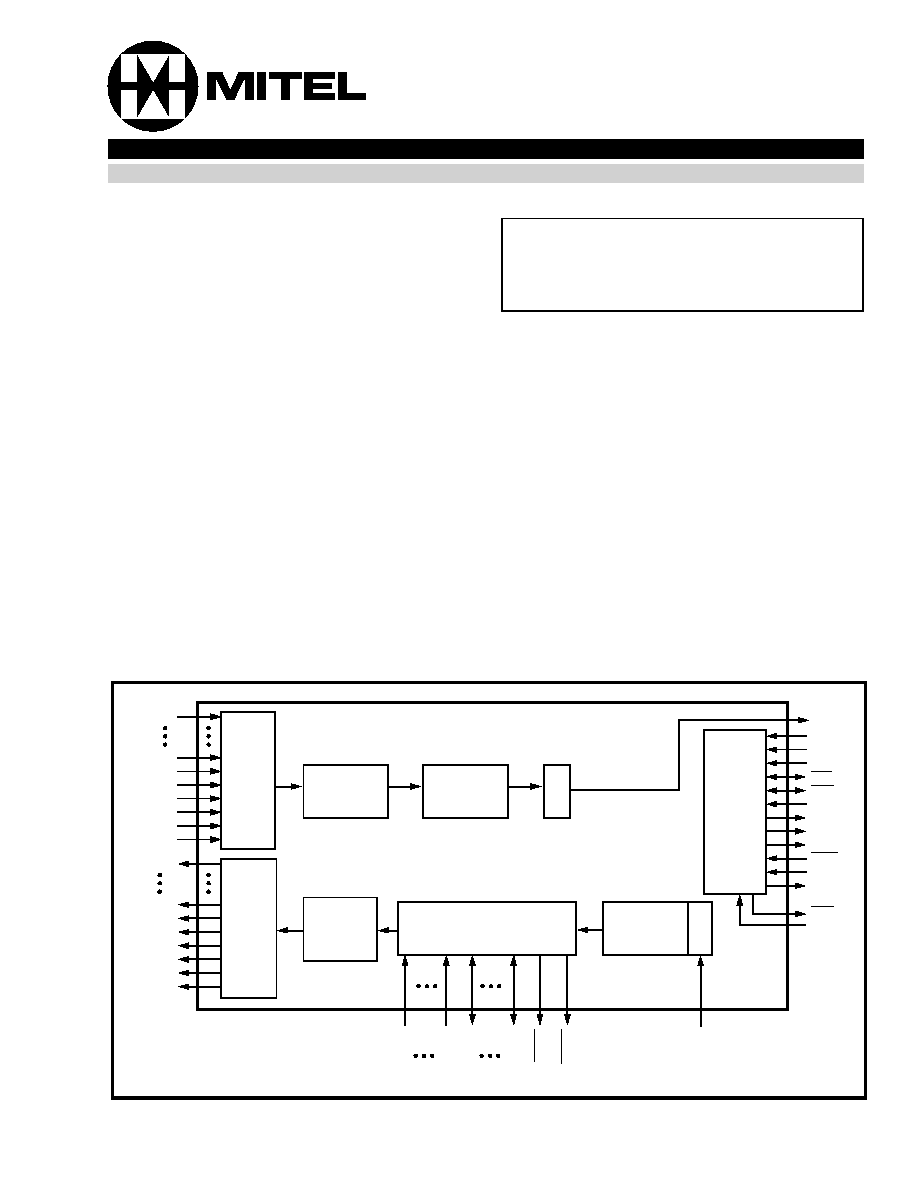
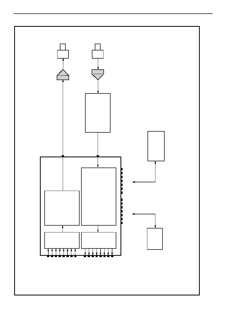
Description
The High-Speed Isochronous Multiplexer integrated
circuit multiplexes up to eight Serial Telecom
(ST-BUS) links onto a single 20 MHz loop to facilitate
point-to-point data transport requirements. The
MT90710 connects easily with standard Fiber Optic
interfaces to form a complete electric to photonic
conversion circuit. Optical transmission allows large
bandwidth inter-shelf or, in distributed systems,
inter-node communication by eliminating multiple
data buses, cable inter-connect and attendant driver
interfaces. The final result is a simple physical
interface free of the radiated emissions and
background noise susceptibility problems
encountered in copper-wired environments.
Ordering Information
MT90710AP 84 Pin PLCC
0 ∞C to +70 ∞C
F
BADDR
0
F
BADDR
7
FB
D
A
TA
0
FB
D
A
TA
7
FB
O
E
FBW
E
STi0
STi5
STi6A
STi6B
STi7
DIN8K0
DIN8K1
DIN32K
MUX
STo0
STo5
STo6A
STo6B
STo7
DOUT8K0
DOUT8K1
DOUT32K
DEMUX
Overhead
Checksum
Frame Sync
PI
S
O
4B/5B &
NRZI
Encode
Overhead
Extract &
Insert
Error Check
Frame Alignment & Buffer
External Memory Control
Control
RECEIVE
TRANSMIT
MODE0
MODE1
MODE2
F0b
C4b
E20i
RLED
LLED
C20o
POR
RESET
C4REFo
C4o
C40i
NRZI Decode
Sync Detect
4B/5B Decode
SIP
O
TxDATA
Rx
D
A
T
A
From Receive Pin Diode,
Pre-amp and Post-amp
Circuits
To Transmit Driver
Amplifier and Fiber
Driver Transducer
Signals to
External PLL
ISSUE 1
January 1995
Figure 1 - Functional Block Diagram
CMOS
Preliminary Information
MT90710
Preliminary Information
5-4
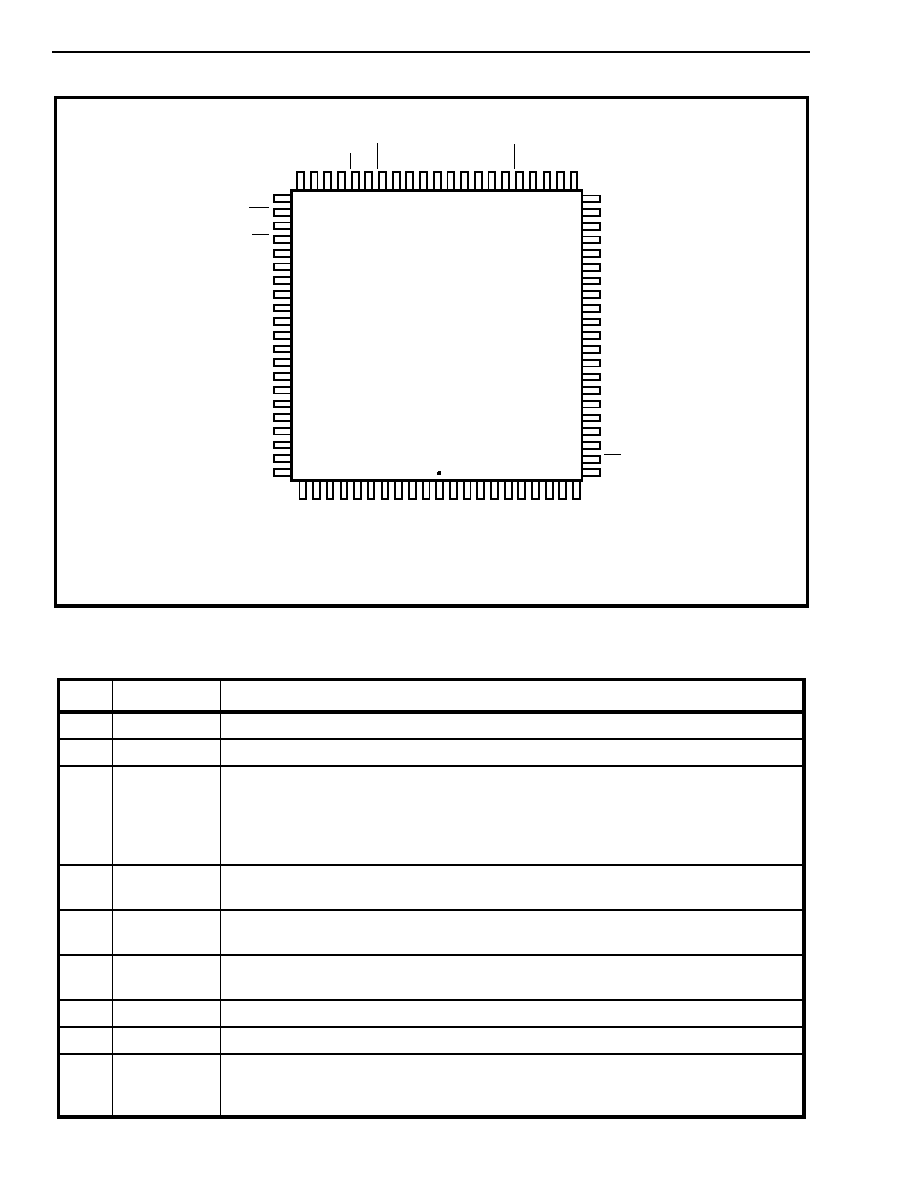
Figure 2 - Pin Connections
Pin Description
Pin #
Name
Description
1
V
SS
Power Supply Ground. Nominally 0 volts.
2
V
DD
Positive Power Supply. Nominally 5 volts.
3
STo7
Serial, 32 Channel, 2.048 Mb/s Link 7 (Output Type 3). Only channels 9 - 31 are
available for user data transfer (1.474 Mb/s). Channels 0 - 8 (0.576 Mb/s) are reserved
for access to fiber overhead information. Output is active only when the receiver
detects the synchronization pattern on RxDATA input stream; output is high impedance
during loss of synchronization.
4
DOUT8K0
Asynchronous 8 kHz Signal 0 (Output Type 3). Sourced from the far-end DIN8K0
input.
5
DOUT8K1
Asynchronous 8 kHz Signal 1 (Output Type 3). Sourced from the far-end DIN8K1
input.
6
C20o
20.48 MHz Clock (Output Type 3). Derived from transmit PLL 40.96 MHz clock divided
by 2 (see pin 18). Made available for system use.
7
NC
No Internal Connection.
8
FBADDR7
Frame Buffer RAM Address Bit 7 (Output Type 2).
9
STo6A
Serial, 32 Channel, 2.048 Mb/s Link 6A (Output Type 3). Output is active only when
the receiver detects the synchronization pattern on RxDATA input stream; output is high
impedance during loss of synchronization.
32
14
16
18
20
22
26
28
30
24
54
70
68
66
64
60
58
56
62
NC
74
72
12
52
50
48
46
44
42
40
38
36
34
76
78
80
82
84
2
4
6
8
10
VSS
F
B
A
DDR0
F
B
A
DDR1
F
B
A
DDR2
F
B
A
DDR3
F
B
A
DDR4
F
B
A
DDR5
F
B
A
DDR6
S
T
o6B
VSS
VD
D
ST
o
7
DO
UT
8K
0
DO
UT
8K
1
C20
o
NC
F
B
A
DDR7
S
T
o6A
ST
o
5
VD
D
NC
VSS
NC
E20i
STi7
STi6B
STi6A
STi5
STi4
STi3
VDD
STi2
C40i
NC
NC
NC
C4REFo
C4o
VSS
VDD
POR
FBDATA7
C4b
DIN8K0
FBDATA4
DIN32K
VDD
STi0
FBDATA2
VSS
FBDATA3
DIN8K1
FBDATA1
LLED
FBDATA0
RESET
IC
VDD
IC
VS
S
Tx
D
A
T
A
DO
UT
32K
F0
b
ST
o
1
FB
W
E
ST
o
4
ST
o
3
VS
S
VD
D
ST
o
0
MO
D
E
0
MO
D
E
1
MO
D
E
2
FB
O
E
RLE
D
Rx
D
A
T
A
NC
VD
D
ST
o
2
84 PIN PLCC
VSS
STi1
FBDATA6
FBDATA5

Preliminary Information
MT90710
5-5
10
STo5
Serial, 32 Channel, 2.048 Mb/s Link 5 (Output Type 3). Output is active only when
the receiver detects the synchronization pattern on RxDATA input stream; output is high
impedance during loss of synchronization.
11
V
DD
Positive Power Supply. Nominally 5 volts.
12
V
SS
Power Supply Ground. Nominally 0 volts.
13
C4o
4.096 MHz Clock (Output Type 3). Used by the transmit PLL. This clock is the input
C40i (40.96MHz, see pin 18) master clock divided by 10 (inverted) and is fed back to
the external PLL circuit as a reference.
14
C4REFo
4.096 MHz Reference Clock (Output Type 3). Used by transmit PLL. When in control-
ler mode this clock is derived from the system C4b (4.096 MHz) clock input (see pin
57). When in peripheral mode this clock is extracted from the receive data on the fiber
port.
15,16,
17
NC
No Internal Connection.
18
C40i
Transmit 40.96 MHz Clock (Input Type 2). Derived from the transmit PLL. This is the
master clock used by the device.
19
STi1
Serial, 32 Channel, 2.048 Mb/s Link 1 (Input Type 1).
20
STi2
Serial, 32 Channel, 2.048 Mb/s Link 2 (Input Type 1).
21
V
SS
Power Supply Ground. Nominally 0 volts.
22
V
DD
Positive Power Supply. Nominally 5 volts.
23
STi3
Serial, 32 Channel, 2.048 Mb/s Link 3 (Input Type 1).
24
STi4
Serial, 32 Channel, 2.048 Mb/s Link 4 (Input Type 1).
25
STi5
Serial, 32 Channel, 2.048 Mb/s Link 5 (Input Type 1).
26
STi6A
Serial, 32 Channel, 2.048 Mb/s Link 6A (Input Type 1).
27
STi6B
Serial, 32 Channel, 2.048 Mb/s Link 6B (Input Type 1).
28
STi7
Serial, 32 Channel, 2.048 Mb/s Link 7 (Input Type 1). Only channels 9 - 31 are avail-
able for user data transfer (1.472 Mb/s). Data input on channels 0 - 8 (0.576 Mb/s) is
ignored by the device. This bandwidth is reserved for fiber overhead information.
29
E20i
Receiver 20.96 MHz Clock (Input Type 2). Extracted clock from the receive data
stream. Divided internally by 5 and phase corrected to frame synch pattern to produce
internal 2.048 MHz data clock for parsing the receive STi streams.
30
NC
No Internal Connection.
31
V
SS
Power Supply Ground. Nominally 0 volts.
32
NC
No Internal Connection.
33
V
DD
Positive Power Supply. Nominally 5 volts.
34
NC
No Internal Connection.
35
RxDATA
Receive 4B/5B, NRZI Encoded Serial Data (Input Type 1).
36
RLED
"Remote Sync" LED Driver (Open Collector, Output Type 3). Drives the "Remote
Sync" LED on/off at approximately a 4 Hz rate when the remote interface is not syn-
chronized. Active only when the local interface is synchronized.
37
FBOE
Frame Buffer Ram Enable (Output Type 2). Generates a low going strobe during
valid RAM read access.
Pin Description
Pin #
Name
Description

MT90710
Preliminary Information
5-6
38
MODE2
Operating Mode Select 2 (Input Type 1). See Table 1.
39
MODE1
Operating Mode Select 1 (Input Type 1). See Table 1.
40
MODE0
Operating Mode Select 0 (Input Type 1). See Table 1.
41
STo0
Serial, 32 Channel, 2.048 Mb/s link 0 (Output Type 3). Output is active only when
receiver detects the synchronization pattern on RxDATA input stream; output is high
impedance during loss of synchronization.
42
V
DD
Positive Power Supply. Nominally 5 volts.
43
V
SS
Power Supply Ground. Nominally 0 volts.
44
STo2
Serial, 32 Channel, 2.048 Mb/s link 2 (Output Type 3). Output active only when
receiver detects the synchronization pattern on RxDATA input stream; high impedance
output during loss of synchronization.
45
STo3
Serial, 32 Channel, 2.048 Mb/s link 3 (Output Type 3). Output active only when
receiver detects the synchronization pattern on RxDATA input stream; high impedance
output during loss of synchronization.
46
STo4
Serial, 32 Channel, 2.048 Mb/s link 4 (Output Type 3). Output active only when
receiver detects the synchronization pattern on RxDATA input stream; high impedance
output during loss of synchronization.
47
FBWE
Frame Buffer RAM Write Enable (Output Type 2). Generates a low going strobe dur-
ing valid RAM write access.
48
STo1
Serial, 32 Channel, 2.048 Mb/s link 1 (Output Type 3). Output active only when
receiver detects the synchronization pattern on RxDATA input stream; high impedance
output during loss of synchronization.
49
F0b
System 8 kHz Reference Frame Pulse (Bi-directional; Input and Output Types 3).
When in controller mode this is an input accepting the system reference pulse. In
peripheral mode this is an output supplying the system an 8 kHz reference frame pulse.
50
DOUT32K
Asynchronous 32 kHz Signal 1 (Open Collector, Output Type 3). Sourced from the
far-end DIN32K input.
51
TxDATA
Transmit 4B/5B, NRZI Encoded Serial Data (Output Type 3).
52
V
SS
Power Supply Ground. Nominally 0 volts.
53
IC
Internally Connected (Output Type 1). Drives continuous logic 1. Leave open circuit.
54
V
DD
Positive Power Supply. Nominally 5 volts.
55
POR
Power On Reset (Input Type 2). Active low.
56
FBDATA7
Frame Buffer Data Bit 7 (Bidirectional; Input Type 1 and Output Type 2). Data bit 7.
57
C4b
4.096 MHz Reference Clock (Bidirectional; Input and Output Types 3). Input used
by PLL in controller mode and derived from the system. In peripheral mode this is an
output supplying the system 4.096 MHz reference clock.
58
FBDATA6
Frame Buffer Data Bit 6 (Bidirectional; Input Type 1 and Output Type 2). Data bit 6.
59
FBDATA5
Frame Buffer Data Bit 5 (Bidirectional; Input Type 1 and Output Type 2). Data bit 5.
60
DIN8K0
Asynchronous 8 kHz Signal 0 (Input Type 1). Transmitted to the far-end DOUT8K0
output.
61
FBDATA4
Frame Buffer Data Bit 4 (Bidirectional; Input Type 1 and Output Type 2). Data bit 4.
Pin Description
Pin #
Name
Description

Preliminary Information
MT90710
5-7
Notes:
All unused inputs should be connected to logic high or low unless otherwise stated. All outputs should be left open circuit when not used.
All output types are CMOS with CMOS logic levels (see DC Electrical Characteristics for Type drive capability).
Input Type 1 has TTL compatible logic levels, Type 2 has CMOS compatible logic levels and Type 3 has TTL Schmitt trigger compatible
logic levels (see DC Electrical Characteristics).
62
DIN32K
Asynchronous 32 kHz Signal (Input Type 1). Transmitted to the far-end DOUT32K
output.
63
V
DD
Positive Power Supply. Nominally 5 volts.
64
V
SS
Power Supply Ground. Nominally 0 volts.
65
FBDATA3
Frame Buffer Data Bit 3 (Bidirectional; Input Type 1 and Output Type 2). Data bit 3.
66
STi0
Serial, 32 Channel, 2.048 Mb/s Link 0 (Input Type 1).
67
FBDATA2
Frame Buffer Data Bit 2 (Bidirectional; Input Type 1 and Output Type 2). Data bit 2.
68
DIN8K1
Asynchronous 8 kHz Signal 1 (Input Type 1). Transmitted to the far-end DOUT8K1
output.
69
FBDATA1
Frame Buffer Data Bit 1 (Bidirectional; Input Type 1 and Output Type 2). Data bit 1.
70
LLED
"Local Sync" LED Driver (Open Collector, Output Type 2). Drives the "Local Sync"
LED on/off at approximately a 4 Hz rate when the local interface is not in
synchronization.
71
FBDATA0
Frame Buffer Data Bit 0 (Bidirectional; Input Type 1 and Output Type 2). Data bit 0.
72
RESET
Reset Control (Input Type 1).
73
IC
Internally Connected.
74
V
DD
Positive Power Supply. Nominally 5 volts.
75
NC
No Internal Connection.
76
V
SS
Power Supply Ground. Nominally 0 volts.
77
FBADDR0
Frame Buffer RAM Address Bit 0 (Output Type 2).
78
FBADDR1
Frame Buffer RAM Address Bit 1 (Output Type 2).
79
FBADDR2
Frame Buffer RAM Address Bit 2 (Output Type 2).
80
FBADDR3
Frame Buffer RAM Address Bit 3 (Output Type 2).
81
FBADDR4
Frame Buffer RAM Address Bit 4 (Output Type 2).
82
FBADDR5
Frame Buffer RAM Address Bit 5 (Output Type 2).
83
FBADDR6
Frame Buffer RAM Address Bit 6 (Output Type 2).
84
STo6B
Serial, 32 Channel, 2.048 Mb/s Link 6B (Output Type 3). Output active only when
receiver detects the synchronization pattern on RxDATA input stream; high impedance
output during loss of synchronization.
Pin Description
Pin #
Name
Description
Overview
The MT90710 multiplexes multiple Serial Telecom
(ST-BUS timing, Figure 7) links onto a single 20 MHz
loop to facilitate point-to-point data transport
requirements. The MT90710 connects easily with
standard Fiber Optic interfaces to form a complete
electric to photonic conversion circuit. Optical
transmission allows large bandwidth inter-shelf or, in
distributed systems, inter-node communication by
eliminating multiple data busses, cable inter-connect
and the attendant driver interfaces. The final result is
a simple physical interface free of the radiated
emissions and background noise susceptibility
problems encountered in copper-wired
environments.
MT90710
Preliminary Information
5-8
The MT90710 provides 15.808 Mb/s clear channel,
user bandwidth in both transmit and receive
directions. In addition, two 8 kHz sampled signals
and one 32 kHz sampled signal are encoded and
transported over the loop as additional user
bandwidth. These asynchronous signals, in
combination with overhead information and clear
channel bandwidth produce an aggregate data rate
of 16.384 Mb/s. After encoding (4B/5B) the final
transmitted baud rate is 20.48 Mbaud.
Transmit
The transmit data interface consists of nine ST-BUS
input links and three asynchronously sampled input
signals. These are STi0 - STi5, STi6A and STi6B,
STi7, DIN8K0, DIN8K1 and DIN32K. Six ST-BUS
input links, STi0-5, each provide 2.048 Mb/s
transparent transmission bandwidth. With ST6MUX
Mode disabled STi6A is also a 2.048 Mb/s link while
STi6B is not used (see ST6MUX description). The
first nine channels of the STi7 input are ignored
leaving the remaining 23 channels for user
bandwidth. This allows a total of 15.808 Mb/s clear
bandwidth for application use. The first nine (576
kb/s) channels of STi7 are made available for
transmitting the three asynchronous signals
combined with fiber overhead information. This
overhead is automatically compiled in the transmit
interface and inserted into these timeslots for
transmission over the fiber interface.
Overhead information includes a frame
synchronization byte, an error count and a checksum
calculated on the previous frame of transmitted data.
Once compiled, the contents of the transmit data
bandwidth is first 4B/5B encoded, then NRZI
encoded before it is applied to the transmit fiber
interface driver via TxDATA. 4B/5B ensures that the
NRZI encoded data will contain a minimum of two
transitions per baud. This is sufficient to allow the far
end to extract the embedded clock information. As a
result of 4B/5B encoding the information bandwidth
of 16.384 Mb/s increases to a total baud rate of
20.48 MBaud/s at the fiber interface.
Incoming ST-BUS link data is latched at the mid-bit
position of the internal timeslot. Since there is a
phase difference between the internal and external
timeslots, due to the operation of the PLL, latching
occurs at approximately the 3/4 bit position of the
external timeslot when in Controller mode. In
Peripheral mode data is latched at the midpoint of
the timeslot. Asynchronous signals DIN8K0-1 are
sampled once per frame (8,000 times per second)
and are intended to convey relatively static
information where a state transition is not time
critical enough that a resolution of one frame is
detrimental. Asynchronous signal DIN32K is
sampled four times per frame (32,000 times per
second) and may be used to transport data at a
higher rate than the other two asynchronous inputs.
As an example, this sampling rate is sufficient to
support 19.2K Baud RS-232 signals (TTL levels) so
that remote programming or loop maintenance may
be performed.
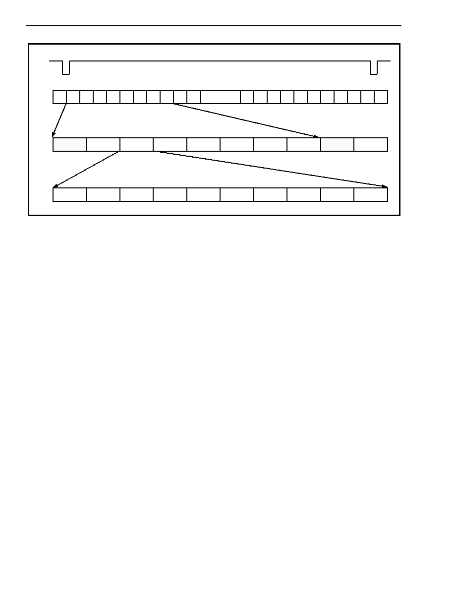
255 0 1 2 3 4 5 6 7 8 9 .......... 246 247 248 249 250 251 252 2
Fiber Timeslot
Channel Assignment
Bit 9 Bit 8 Bit 7 Bit 6 Bit 5 Bit 4 Bit 3 Bit 2 Bit 1 Bit 0
4B/5B Encoded Data Bit Assignment
Frame Pulse
ST6 Ch0 ST5 Ch0 ST4 Ch0 ST3 Ch0 ST2 Ch0 ST1 Ch0 ST0 Ch0 ST6 Ch1
ST7 Ch0
ST7 Ch1
Figure 3 - Fiber Timeslot Assignment
Preliminary Information
MT90710
5-9
Receive
The 4B/5B and NRZI encoded data from the receive
fiber interface is NRZI decoded and the frame
synchronization information is extracted. After 4B/5B
decoding the remaining data is frame aligned either
to the system frame pulse (when in Controller Mode)
or to the extracted frame pulse (when in Peripheral
Mode). After alignment, the received data package is
disassembled into the clear channel ST-BUS
streams, the asynchronous signals and the
overhead/status information. When ST6MUX mode
is disabled, received 15.808 Mb/s bandwidth is made
available on STo0-STo6A and the last 23 channels of
STo7. The asynchronous signals are presented on
DOUT8K0, DOUT8K1 and DOUT32K while the
received overhead information, as well as local
status information, is presented on ST07 in channels
0 to 7.
Control
An external, 40.96 MHz PLL provides the master
clock (C40i) for the MT90710. This PLL uses either
the system's C4b clock (pin 57) for reference when
it's in controller mode or the extracted clock from the
receive data interface when it's in peripheral mode.
Switching between these two primary references is
automatic and under the control of the MODE0-2
pins. The selected reference is fed to the external
PLL from the C4REFo output pin. The MT90710 also
divides the 40.96 MHz master clock by ten and
supplies this secondary reference to the external
PLL on C4o for comparison to the primary reference.
The PLL creates a 40.96 MHz master clock from a
4.096 MHz reference by multiplying by 10 and
attenuates jitter present on the extracted reference.
The master clock is divided down to create internal
clocks, external ST-BUS clocks (when in peripheral
mode) and timeslot counters.
Control signals are also created for the transmitter
and receiver. The transmitter timeslot counter is
synchronized to the backplane frame pulse while the
receiver timeslot counter is sync to the extracted
synchronization pulse.
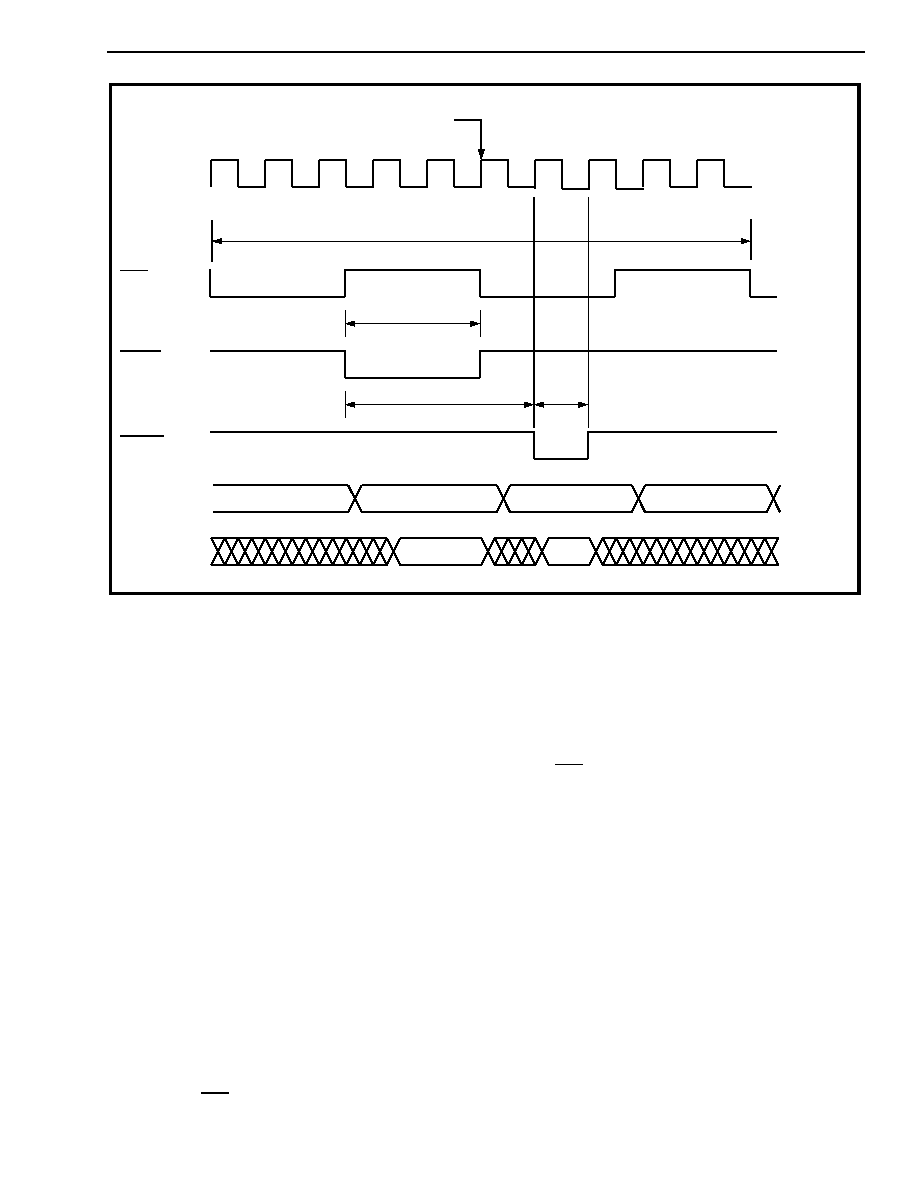
Frame Buffer
To re-align the received data from the fiber interface
to the system, or node, a frame reference buffer is
C4o
(Pin 13)
ST-BUS input data latched here
122 ns
48.8ns
WR
ADDR
RD ADDR
WR ADDR
RD ADDR
RD
WR
FBDATA
FBADDR
FBWE
FBOE
C20o
(Pin 6)
170.8ns
Bit Cell
Figure 4 - Frame Buffer Memory Typical Timing
MT90710
Preliminary Information
5-10
required. This is implemented using an external 8x8
static RAM (35 ns). Only 256 bytes are used of the
8K total. RAM address and data (FBADDR0-7 and
FBDATA0-7) signals are generated along with an
output enable strobe (FBOE) and a write enable
strobe (FBWE).
Table 1 - Operational Mode Select
Overhead Information
Fiber Interface
Eight of the 256 fiber channels are reserved for
overhead information. These are fiber channels:
Channel #
Function
0
Frame Alignment
8
Asynchronous signal transfer and
synchronization detect
16
Checksum of previous frame
24
Reserved
32
Reserved
40
Reserved
48
Remote error count most significant byte
56
Remote error count least significant byte
Mode # Mode 2 Mode 1 Mode 0
ST6MUX
Configuration
0
0
0
0
ENABLED
CONTROLLER
1
0
0
1
ENABLED
PERIPHERAL
2
0
1
0
not used
not used
3
0
1
1
DISABLED CONTROLLER
4
1
0
0
not used
not used
5
1
0
1
not used
not used
6
1
1
0
not used
not used
7
1
1
1
DISABLED
PERIPHERAL
ST-BUS Interface
The first nine STo7 channels are reserved for
overhead information:
STo7 Channel
Function
0
not available
1
not available
2
Reserved
3
Local error count
(most significant byte)
4
Local error count
(least significant byte)
5
Reserved
6
Remote error count
(most significant byte)
7
Remote error count
(least significant byte)
8
synchronization detect
(see STo7 channel 8 definition)
STo7 Channel 8 Definition:
B7
remote receiver is in frame synch
when logic 1
B6
Local receiver is in frame synch
when logic 1
B5, B4, B3
Reserved
B2, B1, B0
Reserved
ST6MUX
ST-BUS to Fiber
When ST6MUX is enabled the STi6A and STi6B
input streams are alternately multiplexed onto the
fiber link. (i.e., only half of the bandwidth of each link
is utilized). The transmit pattern at the fiber interface
is:
STi6A-Chan0,STi6B-Chan1,STi6A-Chan2,STi6B-Chan3,...,
STi6B-Chan29,STi6A-Chan30,STi6B-Chan31
Multiplexed Stream
Chan 0
Chan 1
Chan 2
Chan 3
Chan 4
Chan 5
.....
Chan 28
Chan 29
Chan 30
Chan 31
STo6A Data from STi6A
Chan 0
Chan 0
Chan 2
Chan 2
Chan 4
Chan 4
.....
Chan 28
Chan 28
Chan 30
Chan 30
STo6B Data from STi6B
Chan 1
Chan 1
Chan 3
Chan 3
Chan 5
Chan 5
.....
Chan 29
Chan 29
Chan 31
Chan 31
Table 2 - ST6MUX Channel Assignment
Preliminary Information
MT90710
5-11
Fiber to ST-BUS
When ST6MUX is enabled the STo6A and STo6B
output streams are comprised of the demultiplexed
information received from the fiber link. The received
data is duplicated on two channels since the ST-BUS
channels support twice the bandwidth of the data
from the incoming fiber link. See Table 2.
When ST6MUX is disabled the STi6B and STo6B
ports are not operational. The STi6A and STo6A
ports operate as clear 2.048 MHz links in the same
manner as STi/o links 0 to 5.
Fiber Loop Synchronization
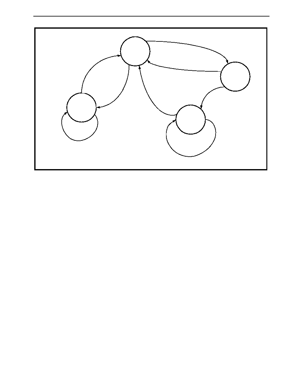
A receiver is declared in synchronization after
detection of three consecutive frames containing a
valid sync pattern. Once synchronized a receiver will
lose sync if a valid sync pattern is not detected in two
of four consecutive frames (refer to Figure 5).
LED Control
The open collector RLED output (pin 36) will cause
an LED, pulled up to +5 volts, to flash at
approximately a 4 Hz rate when the far-end is out of
synchronization but the near-end is synchronized. If
the near-end is not synchronized this output is
inactive.
The open collector LLED output (pin 70) will cause
an LED, pulled up to +5 volts, to flash at
approximately a 4 Hz rate when the near-end is out
of synchronization.
Checksum Generator
Checksum =
Where i-1 is the carry out from the previous
operation. The checksum is calculated on all 255
channels except on channel 0 where the frame
synchronization code is transported. During this
channel the previous checksum is stored and the
register initialized for the next calculation.
DATAi Ci 1
≠
+
i
1
=
255
INCORRECT SYNC
SET SYNC = FALSE
CORRECT SYNC
SET SYNC = FALSE
CORRECT SYNC
SET SYNC = LAST STATE
INCORRECT SYNC
SET SYNC = LAST STATE
CORRECT SYNC
SET SYNC = TRUE
CORRECT SYNC
SET SYNC = TRUE
INCORRECT SYNC
SET SYNC = TRUE
INCORRECT SYNC
SET SYNC = FALSE
STATE 0
STATE 1
STATE 2
STATE 3
Figure 5 - State Diagram
MT90710
Preliminary Information
5-12
Fr
am
e B
u
ffer
STi
0
STi
1
STi
2
STi
3
STi
4
STi
5
STi
6
STi
7
ST
o0
ST
o1
ST
o2
ST
o3
ST
o4
ST
o5
ST
o6
ST
o7
Tx
D
A
T
A
RxDA
T
A
MUX
DE
MU
X
Checks
um
Fram
es
ynch
4B/
5
B an
d
NRZ
I
Pa
r
a
ll
e
l
-
t
o
-
S
e
r
i
a
l
Sh
if
t
En
c
o
d
e
NRZ
I Dec
o
d
e
S
y
n
c
h Detect
4B/
5
B
Deco
de
S
e
r
i
al
-to-P
aral
l
e
l
Sh
if
t
Er
r
o
r
C
h
e
c
k
Fr
a
m
e
A
lig
n
m
e
n
t
a
nd E
x
t
e
rna
l
B
u
ffe
r
C
o
n
t
ro
lle
r
Cl
o
c
k
C
o
n
t
r
o
l
S
i
gna
l
s
I
n
terface
AAAA
AAAA
AAAA
AAAA
AAAA
AAAA
AAAA
AAAA
AAAA
AAAA
AAAA
AAAA
AAAA
AAAA
AAAA
AAAA
AAAA
AAAA
AAAA
AAAA
AAAA
AAAA
AAAA
AAAA
AAAA
AAAA
AAAA
AAAA
AAAA
AAAA
AAAA
AAAA
AAAA
AAAA
AAAA
AAAA
F
i
b
r
e Recei
ver
a
n
d
Amp
lif
ie
r
T
r
a
n
s
m
it
Amp
l
if
i
e
r
an
d Fi
be
r
T
r
an
sm
i
t
t
e
r
Tr
a
n
s
m
i
t
PL
L
C
l
ock
S
Y
T
E
M
I
N
T
E
R
F
A
C
E
S
Rx Cl
ock Reco
very
an
d
Bit Re
g
e
n
e
r
a
tio
n
Fram
e Bu
f
f
er
RA
M
8K x
8
Fi
gu
re
6
-
T
y
p
i
ca
l
Fi
bre
I
n
t
e
rf
ac
e A
p
pl
i
c
at
i
o
n

Preliminary Information
MT90710
5-13
*
Exceeding these figures may cause permanent damage. Functional operation under these conditions is not guaranteed.
Typical figures are at 25∞C and are for design aid only: not guaranteed and not subject to production testing.
Absolute Maximum Ratings*
Parameter
Symbol
Min
Max
Units
1
DC Supply Voltage
V
DD
- 0.3
7
V
2
Input Voltage
V
i
V
SS
- 0.3
V
DD
+ 0.3
V
3
DC Input Current
I
i
+/- 50
mA
4
Storage Temperature
T
stg
- 65
+ 150
∞
C
Recommended Operating Conditions
Characteristics
Sym
Min
Typ
Max
Units
Test Conditions
1
Input
Voltage
V
DD
4.5
5.5
V
2
Operating Temperature
T
OP
0
+70
∞
C
DC Electrical Characteristics
- Voltages are with respect to ground (V
SS
) unless otherwise stated.
Characteristics
Sym
Min
Typ
Max
Units
Test Conditions
1
Supply Current operating
I
DD
230
276
mA
2
Input HIGH voltage (TTL)
V
IHT
2.0
V
Input Type 1
3
Input LOW voltage (TTL)
V
ILT
0.8
V
Input Type 1
4
Input HIGH voltage (CMOS)
V
IHC
0.7V
DD
V
Input Type 2
5
Input LOW voltage (CMOS)
V
ILC
0.3V
DD
V
Input Type 2
6
Positive threshold (schmitt)
V
+
2.0
V
Input Type 3
7
Negative threshold (schmitt)
V
-
0.8
V
Input Type 3
8
Hysteresis
V
H
0.5
V
Input Type 3
9
Input leakage current
I
IH
/I
IL
150
µ
A
V
DD
=5.5V,
V
IN
=V
SS
to V
DD
10
High level output voltage
V
OH
3.7
V
All output types @ max I
11
Low level output voltage
V
OL
0.4
V
All output types @ max I
12
Output Current
I
O1
I
O4
I
O12
1
4
12
mA
mA
mA
Output Type 1
Output Type 2
Output Type 3
13
High impedance leakage
I
OZ
20
µ
A
V
DD
=5.5V,
V
IN
=V
SS
to V
DD
14
Output capacitance
C
o
20
pF
15
Input capacitance
C
i
7
20
pF
MT90710
Preliminary Information
5-14
Timing is over recommended temperature & power supply voltages (V
DD
=5V±10%, V
SS
=0V, T
A
=0 to 70∞C).
Typical figures are at 25∞C and are for design aid only: not guaranteed and not subject to production testing.
Figure 7 - ST-BUS Timing
AC Electrical Characteristics
- ST-BUS Timing
Voltages are with respect to ground (V
SS
) unless otherwise stated.
Characteristics
Sym
Min
Typ
Max
Units
Test Conditions
1
Frame Pulse width
t
F0iW
244
ns
2
Frame Pulse setup time
t
F0iS
10
190
ns
3
Frame Pulse hold time
t
F0iH
20
190
ns
4
STo delay Active to Active
t
DAA
45
100
ns
C
L
=150 pF
5
STi setup time
t
STiS
20
ns
6
STi hold time
t
STiH
20
ns
7
Clock period
t
C4i
200
244
300
ns
8
CK Input Low
t
CL
85
122
150
ns
9
CK Input High
t
CH
85
122
150
ns
10 Clock Rise/Fall Time
t
r,
t
f
10
ns
2.0V
0.8V
STi
2.0V
0.8V
2.0V
0.8V
STo
2.0V
0.8V
F0i
t
F0iW
t
C4i
t
CH
t
CL
t
F0iS
t
DAA
t
STiS
t
STiH
t
F0iH
Ch. 31
Bit 0
Ch. 0
Bit 7
Ch. 0
Bit 6
Ch. 31
Bit 0
Ch. 0
Bit 7
Ch. 0
Bit 6
Ch. 0
Bit 5
Ch. 0
Bit 5
C4i
t
f
t
r