1
Features
∑
2,048
◊
512 and 512 x 512 switching among
backplane and local streams
∑
Rate conversion between 2.048, 4.096 and
8.192Mb/s
∑
Optioal sub-rate switch configuration for
2.048 Mb/s streams
∑
Per-channel variable or constant throughput
delay
∑
Compatible to HMVIP and H.100 specifications
∑
Automatic frame offset delay measurement
∑
Per-stream frame delay offset programming
∑
Per-channel message mode
∑
Per-channel direction control
∑
Per-channel high impedance output control
∑
Non-multiplexed microprocessor interface
∑
Connection memory block programming
∑
3.3V local I/O with 5V tolerant inputs and
TTL-compatible outputs
∑
IEEE-1149.1 (JTAG) Test Port
Applications
∑
Medium and large switching platforms
∑
CTI application
∑
Voice/data multiplexer
∑
Support ST-BUS, HMVIP and H.100 interfaces
Description
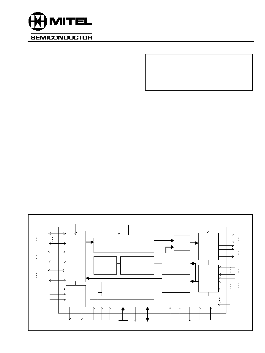
The MT90863 Rate Conversion Switch provides
switching capacities of 2,048
◊
512 channels
between backplane and local streams, and 512 x
512 channels for local streams. The connected serial
inputs and outputs may have 32, 64 and 128 64kb/s
channels per frame with data rates of 2.048Mb/s,
4.096Mb/s and 8.192Mb/s respectively.
The MT90863 also offers a sub-rate switching
configuration which allows 2-bit wide 16kb/s data
channels to be switched within the device.
The device has features (such as: message mode;
input and output offset delay; direction control; and,
high impedance output control) that are
programmable on per-stream or per-channel basis.
Figure 1 - Functional Block Diagram
F0o
DS CS R/W
A7-A0
DTA D15-D0
C16i
Test Port
Output
Mux
Microprocessor Interface
Timing
Unit
Internal
Backplane
Connection
Data Memory
ODE
V
SS
V
DD
TDI TDO
RESET
TCK TRST
TMS
Interface
Backplane
Converter
P/S
&
S/P
F0i
C4i/C8i
C4o
STo0
STo11
STo12
STo13
STo15
STi0
STi11
STi12
STi13
STi15
(2,048 channels)
(2,048 locations)
Local
Memory High/Low
(512 locations)
Multiple Buffer
Data Memory
(512 channels)
Multiple Buffer
Data Memory
(512 channels)
Registers
IC1
ODE
P/S
Converter
Local
Interface
S/P
Converter
Local
Interface
STio0/
STio15/
FEi15
FEi0
STio16/
STio23/
FEi23
FEi16
STio24
STio31
IC2
Connection
Memory
Multiple Buffer
Ordering Information
MT90863AL1
128 Pin MQFP
MT90863AG1
144 Pin BGA
-40 to +85 C
DS5034
ISSUE 3
March 1999
MT90863
3V Rate Conversion Digital Switch
Advance Information
MT90863
Advance Information
2
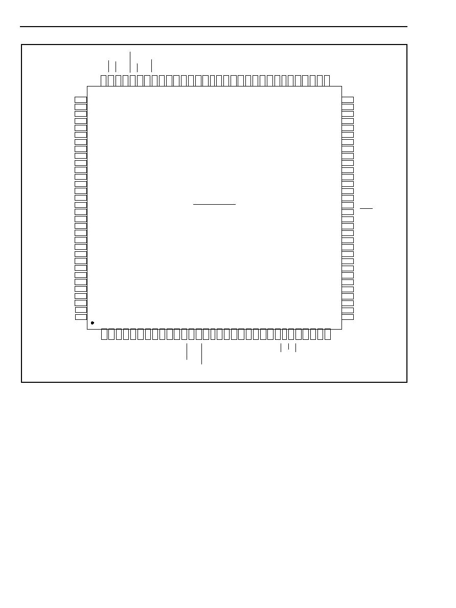
Figure 2 - MQFP Pin Connections
128 Pin PQFP
79
85
87
89
71
73
75
77
93
67
91
69
65
83
81
95
111
117
119
121
103
105
107
109
125
99
123
101
97
115
113
127
49
47
45
43
41
57
59
55
53
51
39
37
35
61
63
33
17
11
9
7
25
23
21
19
3
29
5
27
31
13
15
1
D14
D12
D11
D10
D9
D8
D6
D5
D4
D3
D2
DTA
D13
D15
STi13
STi12
STi11
STi10
STi9
STi8
STi7
STi6
STi4
STi3
STi2
STi1
STi0
STi5
VDD
VSS
VSS
D7
VDD
STo0
STo1
STo2
STo3
STo4
STo5
STo6
STo7
VSS
VDD
ODE
STo8
STo9
STo10
STo11
STo12
STo13
STo14
ST015
VSS
VSS
F0i
F0o
C4o
VSS
C16i
VSS
VSS
STi14
STi15
STio0/FEi0
STio1/FEi1
STio2/FEi2
STio3/FEi3
STio4/FEi4
STio5/FEi5
STio6/FEi6
STio7/FEi7
STio8/FEi8
STio9/FEi9
STio11/FEi11
STio15/FEi15
STio10/FEi10
STio12/FEi12
STio13/FEi13
STio14/FEi14
STio16/FEi16
STio17/FEi17
STio18/FEi18
STio19/FEi19
STio20/FEi20
VSS
VDD
STio21/FEi21
STio22/FEi22
STio23/FEi23
STio24
VDD
VSS
VDD
VSS
VDD
R/
W
TCK
TDO
A6
A5
A4
A3
A2
A1
A0
DS
A7
TDI
D1
D0
VDD
TRST
IC1
TMS
RESET
VSS
STio25
STio26
STio27
STio28
STio29
STio30
STio31
VSS
VSS
CS
IC2
C4i/C8i
Advance Information
MT90863
3
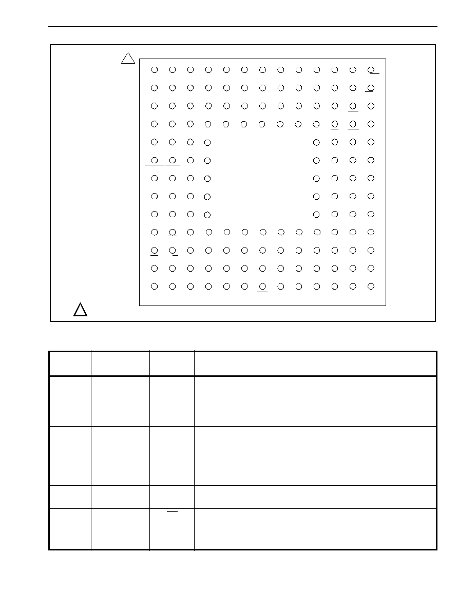
Figure 3 - BGA Pin Connections
Pin Description
128 MQFP
Pin#
144 BGA
Pin#
Name
Description
30,50,67,
79,97,107,
117,127
C5,C9,D5,D7,
D9,E10,F4,G10
,G11,H4,
K3,K4,K6,K8
K10,K11,L8
V
DD
+3.3 Volt Power Supply
8,17,29,39,
49,68,78,8
8,90,93,96,
106,
116,126
C6,C10,D4,D6,
D8,D10,E3,E4,
F10,F11,G2,
G4,H10,J4,
J10,J11,K5
K7,K9,L3,L7
V
ss
Ground
89
D12
C16i
Master Clock (5V Tolerant Input): Serial clock for shifting data in/out
on the serial streams. This pin accepts a 16.384 MHz clock.
91
D11
F0i
Master Frame Pulse (5V Tolerant Input): In ST-BUS mode, this input
accepts a 61ns wide negative frame pulse. In CT Bus mode, it accepts
a 122ns wide negative frame pulse. In HMVIP mode, it accepts a
244ns wide negative frame pulse.
1 - A1 corner is identified by metallized markings.
B
C
D
E
F
G
H
J
K
L
M
N
1
2
3
4
5
6
7
8
9
10
11
12
13
TOP VIEW
1
A
STio25
STio26
STio27
STio28
STio29
STio30
STio31
TMS
TDI
TDO
TCK
TRST
IC1
RESET
A0
A1
A2
A3
A4
A5
A6
A7
DS
R/W
CS
D0
D1
D2
D3
D4
D5
D6
D7
D8
D9
D10
D11
D12
D14
D13
D15
DTA
STi0
STi1
STi2
STi3
STi4
STi5
STi6
STi7
STi8
STi9
STi10
STi11
STi12
STi13 STi14
STi15 ODE
STo0
STo1
STo2
STo3
STo4
STo5
STo6
STo7
STo8
STo9
STo10
STo11
STo12
STo13
STo14
STo15
C16i
F0i
C4i/C8i
C4o
F0o
STio0
STio1
STio2
STio3
STio4
STio5
STio6
STio7
STio8
STio9
STio10
STio11
STio12
STio13
STio14
STio15
STio16
STio17
STio18
STio19
STio20
STio21
STio22
STio23
STio24
VSS
VSS
VSS
VSS
VSS
VSS
VSS
VDD
VDD
VDD
VDD
VDD
VDD
VSS
IC2
VDD
VSS
VDD
VSS
VDD
VSS
VSS
VSS
VDD
VSS
VDD
VSS
VDD
VDD
VSS
VDD
VSS
VSS
VDD
VDD
VSS
VSS
VDD
VSS

MT90863
Advance Information
4
92
B13
C4i/C8i
HMVIP/CT Bus Clock (5V Tolerant Input): When HMVIP mode is
enabled, this pin accepts a 4.096MHz clock for HMVIP frame pulse
alignment. When CT Bus mode is enabled, it accepts a 8.192MHz
clock for CT frame pulse alignment.
94
A13
F0o
Frame Pulse (5V Tolerant Output): A 244ns wide negative frame
pulse that is phase locked to the master frame pulse (F0i).
95
C12
C4o
C4 Clock (5V Tolerant Output): A 4.096MHz clock that is phase
locked to the master clock (C16i).
98-105,
108-115
C11, B12, B11,
A12, A11, B10,
A10, B9, A9,
C8, B8, A8, C7,
B7, A7, A6,
STio0 - 15
FEi0 - 15
Serial Input Streams 0 to 15 / Frame Evaluation Inputs 0 to 15 (5V
Tolerant I/O). In 2Mb/s and HMVIP modes, these pins accept serial
TDM data streams at 2.048 Mb/s with 32 channels per stream. In 4Mb/
s or 8Mb/s mode, these pins accept serial TDM data streams at 4.096
or 8.192 Mb/s with 64 or 128 channels per stream respectively. In
Frame Evaluation Mode (FEM), they are frame evaluation inputs.
118-125
B6, A5, B5, A4,
B4, C4, A3, B3
STio16 - 23
FEi16 - 23
Serial Input Streams 16 to 23 (5V Tolerant I/O). In 2Mb/s or 4Mb/s
mode, these pins accept serial TDM data streams at 2.048 or 4.096
Mb/s with 32 or 64 channels per stream respectively. In HMVIP mode,
these pins have a data rate of 8.192Mb/s with 128 channels per
stream. In Frame Evaluation Mode (FEM), they are frame evaluation
inputs.
128,
1-7
A2, B2, A1, C3,
C2, B1, D3, D2
STio24 - 31 Serial Input Streams 24 to 31 (5V Tolerant I/O). These pins are only
used for 2Mb/s or 4Mb/s mode. They accept serial TDM data streams
at 2.048 or 4.096 Mb/s with 32 or 64 channels per stream respectively.
9
C1
TMS
Test Mode Select (3.3V Input with internal pull-up): JTAG signal
that controls the state transitions of the TAP controller.
10
D1
TDI
Test Serial Data In (3.3V Input with internal pull-up): JTAG serial
test instructions and data are shifted in on this pin.
11
E2
TDO
Test Serial Data Out (3.3V Output): JTAG serial data is output on this
pin on the falling edge of TCK. This pin is held in a high impedance
state when JTAG scan is not enabled.
12
E1
TCK
Test Clock (5V Tolerant Input): Provides the clock to the JTAG test
logic.
13
F2
TRST
Test Reset (3.3 V Input with internal pull-up): Asynchronously
initializes the JTAG TAP controller by putting it in the Test-Logic-Reset
state. This pin should be pulsed low on power-up, or held low
continuously, to ensure that the MT90863 is in the normal operation
mode.
14
F3
IC1
Internal Connection 1 (3.3V Input with internal pull-down):
Connect to V
SS
for normal operation.
15
F1
RESET
Device Reset (5V Tolerant Input): This input (active LOW) puts the
MT90863 in its reset state. This clears the device's internal counters
and registers. It also brings microport data bus STio0 - 31 and STo0 -
15 to a high impedance state.
16
G3
IC2
Internal Connection 2 (3.3V Input):
Connect to V
SS
for normal operation.
Pin Description (continued)
128 MQFP
Pin#
144 BGA
Pin#
Name
Description
Advance Information
MT90863
5
18-25
G1, H1, H2,
H3, J2, J1,J3,
K1
A0 - A7
Address 0 - 7 (5V Tolerant Input): These lines provide the A0 to A7
address lines to the internal memories.
26
K2
DS
Data Strobe (5V Tolerant Input): This active low input works in
conjunction with CS to enable the read and write operations.
27
L2
R/W
Read/Write (5V Tolerant Input): This input controls the direction of
the data bus lines (D0-D15) during a microprocessor access.
28
L1
CS
Chip Select (5V Tolerant Input): Active low input used by a
microprocessor to activate the microprocessor port.
31-38,
40-47
M1, N1, M2, N2,
M3, L4, N3, L5,
M4, N4, M5,
L6, M6, N5, N6,
M7,
D0 - 7,
D8 - D15
Data Bus 0 -15 (5V Tolerant I/O): These pins form the 16-bit data bus
of the microprocessor port.
48
N7
DTA
Data Transfer Acknowledgment (5V Tolerant Three-state Output):
This active low output indicates that a data bus transfer is complete. A
pull-up resistor is required to hold a HIGH level when the pin is tri-
stated.
51-54
N8, M8, N9,
N10
STi0 - 3
Serial Input Streams 0 to 3 (5V Tolerant Inputs): In 2Mb/s or
Subrate Switching mode, these inputs accept data rates of 2.048 Mb/s
with 32 channels per stream. In 8Mb/s mode, these inputs accept data
rates of 8.192 Mb/s with 128 channels per stream.
55-62
M9, N11, L9,
M10, L10, N12,
M11, N13
STi4 - 11
Serial Input Streams 4 to 11 (5V Tolerant Inputs): In 2Mb/s or Sub-
rate Switching mode, these inputs accept data rates of 2.048Mb/s
with 32 channels per stream.
63
L11
STi12
Serial Input Streams 12 (5V Tolerant Input): In 2Mb/s mode, this
input accepts data rate of 2.048Mb/s with 32 channels per stream
respectively. In Sub-rate Switching mode, this pin accepts 2.048Mb/s
with 128 channels per stream for Sub-rate switching application.
64-66
M12, M13, L12
STi13 - 15 Serial Input Streams 13 to 15 (5V Tolerant Inputs): In 2Mb/s mode,
these inputs accept a data rate of 2.048Mb/s with 32 channels per
stream.
69
L13
ODE
Output Drive Enable (5V Tolerant Input): This is the output enable
control for the STo0 to STo15 serial outputs and STio0 to STio31 serial
bidirectional outputs.
70-73
K13, K12, J13,
J12
STo0 - 3
Serial Output Streams 0 to 3 (5V Tolerant Three-state Outputs): In
2Mb/s or Sub-rate Switching mode, these outputs have data rates of
2.048 Mb/s with 32 channels per stream respectively. In 8Mb/s mode,
these outputs have data rates of 8.192 Mb/s with 128 channels per
stream
74-77,
80-83
H11, H13, H12,
G13, G12, F13,
F12, E13
STo4 - 7,
STo8 - 11
Serial Output Streams 4 to 11 (5V Tolerant Three-state Outputs):
In 2Mb/s or Sub-rate Switching mode, these outputs have data rates of
2.048Mb/s with 32 channels per stream
Pin Description (continued)
128 MQFP
Pin#
144 BGA
Pin#
Name
Description