 | –≠–ª–µ–∫—Ç—Ä–æ–Ω–Ω—ã–π –∫–æ–º–ø–æ–Ω–µ–Ω—Ç: MT9126 | –°–∫–∞—á–∞—Ç—å:  PDF PDF  ZIP ZIP |
8-33
Æ
Features
∑
Full duplex transcoder with four encode
channels and four decode channels
∑
32 kb/s, 24 kb/s and 16 kb/s ADPCM coding
complying with ITU-T (previously CCITT) G.726
(without 40 kb/s), and ANSI T1.303-1989
∑
Low power operation, 25 mW typical
∑
Asynchronous 4.096 MHz master clock
operation
∑
SSI and ST-BUS interface options
∑
Transparent PCM bypass
∑
Transparent ADPCM bypass
∑
Linear PCM code
∑
No microprocessor control required
∑
Simple interface to Codec devices
∑
Pin selectable
µ-
Law or A-Law operation
∑
Pin selectable ITU-T or signed magnitude PCM
coding
∑
Single 5 volt power supply
Applications
∑
Pair gain
∑
Voice mail systems
∑
Wireless telephony systems
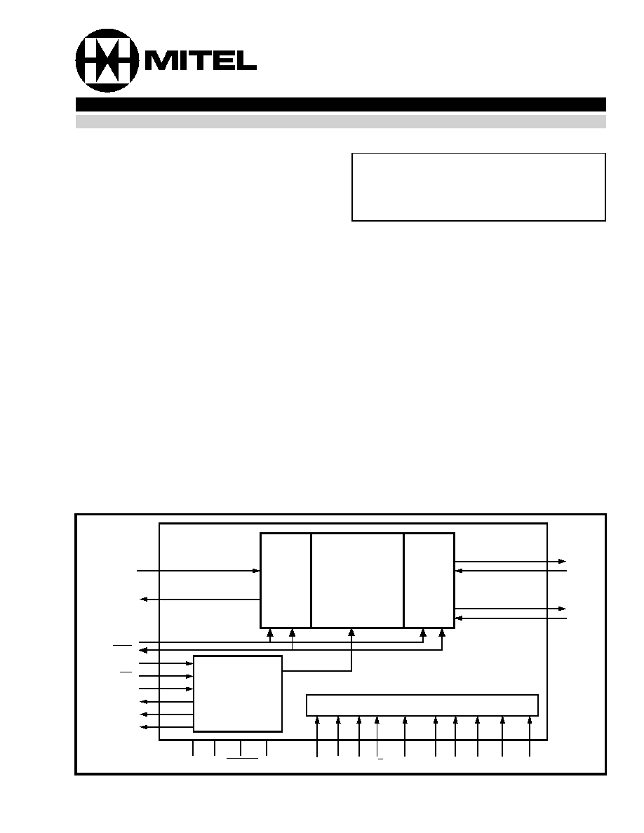
Description
The Quad ADPCM Transcoder is a low power,
CMOS device capable of four encode and four
decode functions per frame. Four 64 kbit/s PCM
octets are compressed into four 32, 24 or 16 kbit/s
ADPCM words, and four 32, 24 or 16 kbit/s ADPCM
words are expanded into four 64 kbit/s PCM octets.
The 32, 24 and 16 kbit/s ADPCM transcoding
algorithms utilized conform to ITU-T
Recommendation G.726 (excluding 40 kbit/s), and
ANSI T1.303 - 1989.
Switching, on-the-fly, between 32 kbit/s and 24 kbit/s
ADPCM, is possible by controlling the appropriate
mode select (MS1 - MS6) control pins. All optional
functions of the device are pin selectable allowing a
simple interface to industry standard codecs, digital
phone devices and Layer 1 transceivers. Linear
coded PCM is provided to facilitate external DSP
functions .
Ordering Information
MT9126AE
28 Pin Plastic DIP
MT9126AS
28 Pin SOIC
-40 ∞C to +85 ∞C
ISSUE 2
May 1995
ADPCM
I/O
PCM
I/O
Control Decode
VDD VSS PWRDN IC
MS1 MS2
A/
µ
FORMAT
MS5
MS4
MS3
MS6 LINEAR SEL
Timing
ADPCMi
ADPCMo
ENB1
ENB2/F0od
BCLK
F0i
MCLK
C2o
EN1
EN2
PCMo1
PCMi1
PCMo2
PCMi2
Full Duplex
Quad
Transcoder
Figure 1 - Functional Block Diagram
MT9126
Quad ADPCM Transcoder
Preliminary Information
CMOS

MT9126
Preliminary Information
8-34
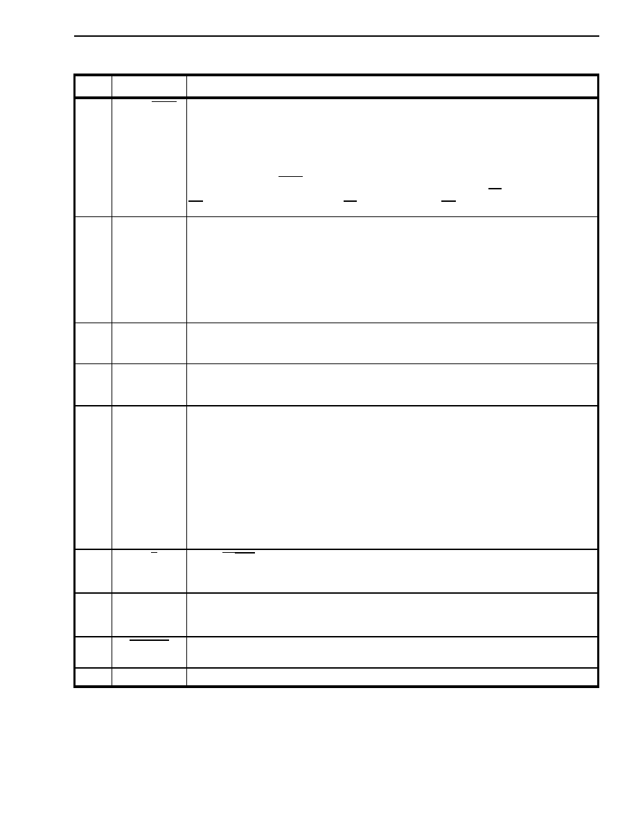
Figure 2 - Pin Connections
Pin Description
Pin #
Name
Description
1
EN1
Enable Strobe 1 (Output). This 8 bit wide, active high strobe is active during the B1
PCM channel in ST-BUS mode. Becomes a single bit, high true pulse when LINEAR=1.
In SSI mode this output is high impedance.
2
MCLK
Master Clock (input). This is a 4.096 MHz (minimum) input clock utilized by the
transcoder function; it must be supplied in both ST-BUS and SSI modes of operation.
In ST-BUS mode the C4 ST-BUS clock is applied to this pin. This synchronous clock is
also used to control the data I/O flow on the PCM and ADPCM input/output pins
according to ST-BUS requirements.
In SSI mode this master clock input is derived from an external source and may be
asynchronous with respect to the 8 kHz frame. MCLK rates greater than 4.096 MHz are
acceptable in this mode since the data I/O rate is governed by BCLK.
3
F0i
Frame Pulse (Input). Frame synchronization pulse input for ST-BUS operation. SSI
operation is enabled by connecting this pin to V
SS
.
4
C2o
2.048 MHz Clock (Output). This ST-BUS mode bit clock output is the MCLK (C4) input
divided by two, inverted, and synchronized to F0i. This output is high-impedance during
SSI operation.
5
BCLK
Bit Clock (Input). 128 kHz to 4096 kHz bit clock input for both PCM and ADPCM ports;
used in SSI mode only. The falling edge of this clock latches data into ADPCMi, PCMi1
and PCMi2. The rising edge clocks data out on ADPCMo, PCMo1 and PCMo2. This input
must be tied to V
SS
for ST-BUS operation.
6
PCMo1
Serial PCM Stream 1 (Output). 128 kbit/s to 4096 kbit/s serial companded/linear PCM
output stream. Data are clocked out by rising edge of BCLK in SSI mode. Clocked out by
MCLK divided by two in ST-BUS mode. See Figure 14.
7
PCMi1
Serial PCM Stream 1 (Input). 128 kbit/s to 4096 kbit/s serial companded/linear PCM
input stream. Data are clocked in on falling edge of BCLK in SSI mode. Clocked in at the
3/4 bit position of MCLK in ST-BUS mode. See Figure 14.
8
V
SS
Digital Ground. Nominally 0 volts.
9
LINEAR
Linear PCM Select (Input). When tied to V
DD
the PCM I/O ports (PCM1,PCM2) are 16-
bit linear PCM. Linear PCM operates only at a bit rate of 2048 kbit/s. Companded PCM is
selected when this pin is tied to V
SS
. See Figures 5 & 8.
1
2
3
4
5
6
7
8
9
10
11
12
13
14
15
16
17
18
19
20
28
27
26
25
24
23
22
21
MS1
VDD
MS3
IC
MS4
FORMAT
MS2
PWRDN
ADPCMi
ADPCMo
MS5
MS6
EN2
PCMo1
BCLK
PCMi1
LINEAR
ENB2/F0od
VSS
C2o
MCLK
F0i
PCMi2
ENB1
PCMo2
EN1
SEL
A/
µ
Preliminary Information
MT9126
8-35
10
ENB2/F0od
PCM B-Channel Enable Strobe 2 (Input) / Delayed Frame Pulse (Output).
SSI operation: ENB2 (Input). An 8-bit wide enable strobe input defining B2 channel
(AD)PCM data. A valid 8-bit strobe must be present at this input for SSI operation. See
Figures 4 & 6.
ST-BUS operation: F0od (Output). This pin is a delayed frame strobe output. When LIN-
EAR=0, this becomes a delayed frame pulse output occurring 64 C4 clock cycles after
F0i and when LINEAR = 1 at 128 C4 clock cycles after F0i . See Figures 7, 8, 9 & 14.
11
ENB1
PCM B-Channel Enable Strobe 1 (Input).
SSI operation: An 8-bit wide enable strobe input defining B1 channel (AD)PCM data. A
valid 8-bit strobe must be present at this input for SSI operation.
ST-BUS operation: When tied to V
SS
transparent bypass of the ST-BUS D- and C- chan-
nels is enabled. When tied to V
DD
the ST-BUS D-channel and C-channel output timeslots
are forced to a high-impedance state.
12
PCMo2
Serial PCM Stream 2 (Output). 128 kbit/s to 4096 kbit/s serial companded/linear PCM
output stream. Clocked out by rising edge of BCLK in SSI mode. Clocked out by MCLK
divided by two in ST-BUS mode. See Figure 14.
13
PCMi2
Serial PCM Stream 2 (Input). 128 kbit/s to 4096 kbit/s serial companded/linear PCM input
stream. Data bits are clocked in on falling edge of BCLK in SSI mode. Clocked in at the
3/4 bit position of MCLK in ST-BUS mode. See Figure 14.
14
SEL
SELECT (Input).
PCM bypass mode: When SEL=0 the PCM1 port is selected for PCM bypass operation
and when SEL=1 the PCM2 port is selected for PCM bypass operation.
See Figures 6 & 9.
16 kbit/s transcoding mode:
SSI Operation - in 16 kbit/s transcoding mode, the ADPCM words are assigned to the I/O
timeslot defined by ENB2 when SEL=1 and by ENB1 when SEL=0. See Figure 4.
ST-BUS operation- in 16 kbit/s transcoding mode, the ADPCM words are assigned to the
B2 timeslot when SEL=1 and to the B1 timeslot when SEL=0. See Figure 9.
15
A/
µ
A-Law/
µ-
Law Select (Input). This input pin selects
µ-
Law companding when set to
logic 0, and A-Law companding when set to logic 1. This control is for all channels .This
input is ignored in Linear mode during which it may be tied to V
SS
or V
DD
.
16
FORMAT
FORMAT Select (Input). Selects ITU-T PCM coding when high and Sign-Magnitude
PCM coding when low. This control is for all channels.This input is ignored in Linear
mode during which it may be tied to V
SS
or V
DD
.
17
PWRDN
Power-down (Input). An active low reset forcing the device into a low power mode
where all outputs are high-impedance and device operation is halted.
18
IC
Internal Connection (Input). Tie to V
SS
for normal operation.
Pin Description
Pin #
Name
Description

MT9126
Preliminary Information
8-36
Notes:
All unused inputs should be connected to logic low or high unless otherwise stated. All outputs should be left open circuit when not used.
All inputs have TTL compatible logic levels except for MCLK which has CMOS compatible logic levels and PWRDN which has Schmitt
trigger compatible logic levels.
All outputs are CMOS with CMOS logic levels (See DC Electrical Characteristics).
19
20
21
MS1
MS2
MS3
Mode Selects 1, 2 and 3 (Inputs). Mode selects for all four encoders.
MS3
MS2
MS1
MODE
0
0
0
32 kbit/s ADPCM
0
0
1
24 kbit/s ADPCM
0
1
0
16 kbit/s ADPCM
in EN1/ENB1 when SEL=0
in EN2/ENB2 when SEL=1
0
1
1
ADPCM Bypass for 32 kbit/s and 24 kbit/s
1
0
0
ADPCM Bypass for 16 kbit/s
1
0
1
PCM Bypass (64 kbit/s) to PCM1 if SEL=0, PCM2 if SEL=1
1
1
0
Algorithm reset (ITU-T optional reset)
1
1
1
ADPCMo disable
22
V
DD
Positive Power Supply. Nominally 5 volts +/-10%
23
ADPCMi
Serial ADPCM Stream ( Input). 128 kbit/s to 4096 kbit/s serial ADPCM word input
stream. Data bits are clocked in on falling edge of BCLK in SSI mode and clocked in on
the 3/4 bit edge of MCLK in ST-BUS mode.
24
ADPCMo
Serial ADPCM Stream (Output). 128 kbit/s to 4096 kbit/s serial ADPCM word output
stream. Data bits are clocked out by rising edge of BCLK in SSI mode and clocked out by
MCLK divided by two in ST-BUS mode.
25
26
27
MS4
MS5
MS6
Mode Selects 4, 5 and 6 (Inputs). Mode selects for all four decoders.
MS6
MS5
MS4
MODE
0
0
0
32 kbit/s ADPCM
0
0
1
24 kbit/s ADPCM
0
1
0
16 kbit/s ADPCM
in EN1/ENB1 when SEL=0
in EN2/ENB2 when SEL=1
0
1
1
ADPCM Bypass for 32 kbit/s and 24 kbit/s
1
0
0
ADPCM Bypass for 16 kbit/s
1
0
1
PCM Bypass (64 kbit/s) to PCM1 if SEL=0, PCM2 if SEL=1
1
1
0
Algorithm reset (ITU-T optional reset)
1
1
1
PCMo1/2 disable
28
EN2
Enable Strobe 2 (Output). This 8 bit wide, active high strobe is active during the B2
PCM channel in ST-BUS mode. Forced to high impedance when LINEAR=1.
Pin Description
Pin #
Name
Description

Preliminary Information
MT9126
8-37
Functional Description
The Quad-channel ADPCM Transcoder is a low
power, CMOS device capable of four encode and
four decode operations per frame. Four 64 kbit/s
channels (PCM octets) are compressed into four 32,
24 or 16 kbit/s ADPCM channels (ADPCM words),
and four 32, 24 or 16 kbit/s ADPCM channels
(ADPCM words) are expanded into four 64 kbit/s
PCM channels (PCM octets). The ADPCM
transcoding algorithm utilized conforms to ITU-T
recommendation G.726 (excluding 40 kb/s), and
ANSI T1.303 - 1989. Switching on-the-fly between
32 and 24 kbit/s transcoding is possible by toggling
the appropriate mode select pins (supports T1
robbed-bit signalling).
All functions supported by the device are pin
selectable. The four encode functions comprise a
common group controlled via Mode Select pins MS1,
MS2 and MS3. Similarily, the four decode functions
form a second group commonly controlled via Mode
Select pins MS4, MS5 and MS6. All other pin
controls are common to the entire transcoder.
The device requires 25 mWatts (MCLK= 4.096 MHz)
typically for four channel transcode operation. A
minimum master clock frequency of 4.096 MHz is
required for the circuit to complete four encode
channels and four decode channels per frame. For
SSI operation a master clock frequency greater than
4.096 MHz and asynchronous, relative to the 8 kHz
frame, is allowed.
The PCM and ADPCM serial busses support both
ST-BUS and Synchronous Serial Interface (SSI)
operation. This allows serial data clock rates from
128 kHz to 4096 kHz, as well as compatibility with
Mitel's standard Serial Telecom BUS (ST-BUS). For
ST-BUS operation, on chip channel counters provide
channel enable outputs as well as a 2048 kHz bit
clock output which may be used by down-stream
devices utilizing the SSI bus interface.
Linear coded PCM is also supported. In this mode
the encoders compress, four 14-bit, two's
complement (S,S,S,12,...,1,0), uniform PCM
channels into four 4, 3 or 2 bit ADPCM channels.
Similarly, the decoder expands four 4, 3 or 2 bit
ADPCM channels into four 16-bit, two's complement
(S,14,...,1,0), uniform PCM channels. The data rate
for both ST-BUS and SSI operation in this mode is
2048 kbit/s.
Serial (AD)PCM Data I/O
Serial data transfer to/from the Quad ADPCM
transcoder is provided through one ADPCM and two
PCM ports (ADPCMi, ADPCMo, PCMi1, PCMo1,
PCMi2, PCMo2). Data is transferred through these
ports according to either ST-BUS or SSI
requirements. The device determines the mode of
operation by monitoring the signal applied to the F0i
pin. When a valid ST-BUS frame pulse (244nSec low
going pulse) is applied to the F0i pin the transcoder
will assume ST-BUS operation. If F0i is tied
continuously to V
SS
the transcoder will assume SSI
operation. Pin functionality in each of these modes is
described in the following sub-sections.
ST-BUS Mode
During ST-BUS operation the C2o, EN1, EN2 and
F0od outputs become active and all serial timing is
derived from the MCLK (C4) and F0i inputs while the
BCLK input is tied to V
SS
. (See Figures 7, 8 & 9.)
Basic Rate "D" and "C" Channels
In ST-BUS mode, when ENB1 is brought low,
transparent transport of the ST-BUS "Basic Rate D-
and C-channels" is supported through the PCMi1
and PCMo1 pins. This allows a microprocessor
controlled device, connected to the PCMi/o1 pins, to
access the "D" and "C" channels of a transmission
device connected to the ADPCMi/o pins. When
ENB1 is brought high, the "D" and "C" channel
outputs are tristated. Basic Rate "D" and "C"
channels are not supported in LINEAR mode.(See
Figure 7.)
SSI Mode
During SSI operation the BCLK, ENB1 and ENB2/
F0od inputs become active. The C2o, EN1, and EN2
outputs are forced to a high-impedance state except
during LINEAR operation during which the EN1
output remains active. (See Figures 4, 5 & 6.)
The SSI port is a serial data interface, including data
input and data output pins, a variable rate bit clock
input and two input strobes providing enables for
data transfers. There are three SSI I/O ports on the
Quad ADPCM; the PCMi/o1 PCM port, the PCMi/o2
PCM port, and the ADPCMi/o port. The two PCM
ports may transport 8-bit companded PCM or 16-bit
linear PCM. The alignment of the channels is
determined by the two input strobe signals ENB1
and ENB2/F0od. The bit clock (BCLK) and input
strobes (ENB1 and ENB2/F0od) are common for all

MT9126
Preliminary Information
8-38
three of the serial I/O ports. BCLK can be any
frequency between 128 kHz and 4096 kHz
synchronized to the input strobes. BCLK may be
discontinuous outside of the strobe boundaries
except when LINEAR=1. In LINEAR mode, BCLK
must be 2048 kHz and continuous for 64 cycles after
the ENB1 rising edge and for the duration of ENB2/
F0od.
Mode Select Operation (MS1, MS2, MS3,
MS4, MS5, MS6)
Mode Select pins MS1, MS2 and MS3 program
different bit rate ADPCM coding, bypass, algorithmic
reset and disable modes for all four encoder
functions simultaneously. When 24 kbit/s ADPCM
mode is selected bit 4 is unused while in 16 kb/s
ADPCM mode all ADPCM channels are packed
contiguously into one 8-bit octet. Mode Select pins
MS4, MS5 and MS6 operate in the same manner for
the four decode functions. The mode selects must be
set up according to the timing constraints illustrated
in Figures 16 and 17.
32 kbit/s ADPCM Mode
In 32 kbit/s ADPCM mode, the 8-bit PCM octets of
the B1, B2, B3 and B4 channels (PCMi1 and PCMi2)
are compressed into four 4-bit ADPCM words on
ADPCMo. Conversely, the 4-bit ADPCM words of the
B1, B2, B3 and B4 channels from ADPCMi are
expanded into four 8-bit PCM octets on PCMo1 and
PCMo2. The 8-bit PCM octets (A-Law or
µ
-Law) are
transferred most significant bit first starting with b7
and ending with b0. ADPCM words are transferred
most significant bit first starting with I1 and ending
with I4 (See Figures 4 & 7). Reference ITU-T G.726
for I-bit definitions.
24 kbit/s ADPCM Mode
In 24 kbit/s mode PCM octets are transcoded into 3-
bit words rather than the 4-bit words utilized in 32
kbit/s ADPCM. This is useful in situations where
lower bandwidth transmission is required. Dynamic
operation of the mode select control pins will allow
switching from 32 kbit/s mode to 24 kbit/s mode on a
frame by frame basis. The 8 bit PCM octets (A-Law
or
µ
-Law) are transferred most significant bit first
starting with b7 and ending with b0. ADPCM words
are transferred most significant bit first starting with
I1 and ending with I3 (I4 becomes don't care). (See
Figures 4 & 7.)
16 kbit/s ADPCM Mode
When SEL is set to 0, the 8-bit PCM octets of the B1,
B2, B3 and B4 channels (PCMi1 and PCMi2) are
compressed into four 2-bit ADPCM words on
ADPCMo during the ENB1 timeslot in SSI mode and
during the B1 timeslot in ST-BUS mode. Similarily,
the four 2-bit ADPCM words on ADPCMi are
expanded into four 8-bit PCM octets (on PCMo1 and
PCMo2) during the ENB1/B1 timeslot. (See Figures 4
& 7.)
When SEL is set to 1, The same conversion takes
place as described when SEL = 0 except that the
ENB2/B2 timeslots are utilized.
A-Law or
µ
-Law 8-bit PCM are received and
transmitted most significant bit first starting with b7
and ending with b0. ADPCM data are most
significant bit first starting with I1 and ending with I2.
ADPCM BYPASS (32 and 24 kbit/s)
In ADPCM bypass mode the B1 and B2 channel
ADPCM words are bypassed (with a two-frame
delay) to/from the ADPCM port and placed into the
most significant nibbles of the PCM1/2 port octets.
Note that the SEL pin performs no function for these
two modes (See Figures 6 & 9). LINEAR, FORMAT
and A/
µ
pins are ignored in bypass mode.
In 32 kb/s ADPCM bypass mode, Bits 1 to 4 of the
B1, B2, B3 and B4 channels from PCMi1 and PCMi2
are transparently passed, with a two frame delay, to
the same channels on ADPCMo. In the same
manner, the B1, B2, B3 and B4 channels from
ADPCMi are transparently passed, with a two frame
delay, to the same channels on PCMo1 and PCMo2
pins. Bits 5 to 8 are don't care. This feature allows
two voice terminals, which utilize ADPCM
transcoding, to communicate through a system
without incurring unnecessary transcode
conversions. This arrangement allows byte-wide or
nibble-wide transport through a switching matrix.
24 kb/s ADPCM bypass mode is the same as 32 kb/s
mode bypass excepting that only bits 1 to 3 are
bypassed and bits 4 to 8 are don't care.
ADPCM BYPASS (16 kbit/s)
When SEL is set to 0, only bits 1 and 2 of the B1, B2,
B3 and B4 PCM octets (on PCMi1 and PCMi2) are
bypassed, with a two frame delay, to the same
channels on ADPCMo during the ENB1 timeslot in
SSI mode and during the B1 timeslot in ST-BUS

Preliminary Information
MT9126
8-39
mode. Similarily, the four 2-bit ADPCM words on
ADPCMi are transparently bypassed, with a two
frame delay, to PCMo1 and PCMo2 during the ENB1
or B1 timeslot. Bits 3-8 are don't care. (See Figures 6
& 9.)
When SEL is set to 1, the same bypass occurs as
described when SEL = 0 except that the ENB2 or B2
timeslots are utilized.
LINEAR, FORMAT and A/
µ
pins are ignored in
bypass mode.
PCM BYPASS
When SEL is set to 0, the B1 and B2 PCM channels
on PCMi1 are transparently passed, with a two-
frame delay, to the same channels on the ADPCMo.
Simiarily, the two 8-bit words which are on ADPCMi
are transparently passed, with a two-frame delay, to
channels B1 and B2 of PCMo1 while PCMo2 is set
to a high-impedance state.(See Figures 6 & 9.)
When SEL is set to 1, the B3 and B4 channels on
PCMi2 are transparently passed, with a two frame
delay, to the same channels on ADPCMo. Similarily,
the two 8-bit words which are on ADPCMi are
transparently passed, with a two-frame delay, to
channels B3 and B4 of PCMo2. In this case PCMo1
is always high-impedance if ENB1 = 0. If ENB1 = 1
during ST-BUS operation then the D and C channels
are active on PCMo1.
LINEAR, FORMAT and A/
µ
pins are ignored in
bypass mode.
Algorithm Reset Mode
While an algorithmic reset is asserted the device will
incrementally converge its internal variables to the
'Optional reset values' stated in G.726. Algorithmic
reset requires that the master clock (MCLK) and
frame pulse (ENB1/2 or F0i) remain active and that
the reset condition be valid for at least four frames.
Note that this is not a power down mode; see
PWRDN for this function.
ADPCMo & PCMo1/2 Disable
When the encoders are programmed for ADPCMo
disable (MS1 to MS3 set to 1) the ADPCMo output is
set to a high impedance state and the internal
encode function remains active. Therefore
convergence is maintained. The decode processing
function and data I/O remain active.
When the decoders are programmed for PCMo1/2
disable (MS4 to MS6 set to 1) the PCMo1/2 outputs
are high impedance during the B Channel timeslots
and also, during ST-BUS operation, the D and C
channel timeslots according to the state of ENB1.
Therefore convergence is maintained. The encode
processing function and data I/O remain active.
Whenever any combination of the encoders or
decoders are set to the disable mode the following
outputs remain active. A) ST-BUS mode: ENB2/
F0od, EN1, EN2 and C2o. Also the "D" and "C"
channels from PCMo1 and ADPCMo remain active if
ENB1 is set to 0. If ENB1 is brought high then
PCMo1 and ADPCMo are fully tri-stated. B) SSI
mode: When used in the 16-bit linear mode, only the
EN1 output remains active. For complete chip power
down see PWRDN.
Other Pin Controls
16 Bit Linear PCM
Setting the LINEAR pin to logic one causes the
device to change to 16-bit linear (uniform) PCM
transmission on the PCMi/o1 and PCMi/o2 ports.
The data rate for both ST-BUS and SSI operation in
this mode is 2048 kbit/s and all decode and encode
functions are affected by this pin. In SSI mode, the
input channel strobes ENB1 and ENB2/F0od remain
active for 8 cycles of BCLK for an ADPCM transfer.
The EN1 output is high for one BCLK period at the
end of the frame (i.e., during the 256
th
BCLK period).
In ST-BUS mode, the output strobes EN1 and ENB2/
F0od are adjusted to accommodate the required
PCM I/O streams. The EN1 output becomes a single
bit high true pulse during the last clock period of the
frame (i.e., the 256
th
bit period) while ENB2/F0od
becomes a delayed, low true frame-pulse (F0od)
output occuring during the 64
th
bit period after the
EN1 rising edge.
Linear PCM on PCMi1 and PCMi2, are received as
14-bit, two's complement data with three bits of sign
extension in the most significant positions (i.e.,
S,S,S,12,...1,0) for a total of 16 bits. The linear PCM
data transmitted from PCMo1 and PCmo2 are 16-bit,
two's complement data with one sign bit in the most
significant position (i.e., S,14,13,...1,0)
32 and 24 kbit/s ADPCM mode
In 32 kbit/s and 24 kbit/s linear mode, the 16-bit
uniform PCM dual-octets of the B1, B2, B3 and B4
channels (from PCMi1 and PCMi2) are compressed
into four 4-bit words on ADPCMo. The four 4-bit
ADPCM words of the B1, B2, B3 and B4 channels
MT9126
Preliminary Information
8-40
from ADPCMi are expanded into four 16-bit uniform
PCM dual-octets on PCMo1 and PCMo2. 16-bit
uniform PCM are received and transmitted most
significant bit first starting with b15 and ending with
b0. ADPCM data are transferred most significant bit
first starting with I1 and ending with I4 for 32 kbit/s
and ending with I3 for 24 kbit/s operation (i.e., I4 is
don't care).(See Figures 5 & 8.)
16 kbit/sADPCM mode
When SEL is set to 0, the four, 2-bit ADPCM words
are transmitted/received on ADPCMo/i during the
ENB1 time-slot in SSI mode and during the B1
timeslot in ST-BUS mode. When SEL is set to 1, the
four, 2-bit ADPCM words are transmitted/received
on ADPCMo/i during the ENB2 timeslot in SSI mode
and during the B2 timeslot in ST-BUS mode. (See
Figures 5 & 8.)
PCM Law Control (A/µ, FORMAT)
The PCM companding/coding law invoked by the
transcoder is controlled via the A/µ and FORMAT
pins. ITU-T G.711 companding curves, µ-Law and
A-Law, are selected by the A/µ pin (0=µ-Law;
1=A-Law). Per sample, digital code assignment can
conform to ITU-T G.711 (when FORMAT=1) or to
Sign-Magnitude coding (when FORMAT=0). Table 1
illustrates these choices.
Table 1 - Companded PCM
Power Down
Setting the PWRDN pin low will asynchronously
cause all internal operation to halt and the device to
go to a power down condition where no internal
clocks are running. Output pins C2o, EN1, EN2,
PCMo1, PCMo2 and ADPCMo and I/O pin F0od/
ENB2 are forced to a high-impedance state.
Following the reset (i.e., PWRDN pin brought high)
FORMAT
0
1
PCM Code
Sign-
Magnitude
A/µ = 0 or 1
ITU-T (G.711)
(A/µ = 0)
(A/µ = 1)
+ Full Scale
1111 1111
1000 0000 1010 1010
+ Zero
1000 0000
1111 1111 1101 0101
- Zero
0000 0000
0111 1111 0101 0101
- Full Scale
0111 1111
0000 0000 0010 1010
and assuming that clocks are applied to the MCLK
and BCLK pins, the internal clocks will still not begin
to operate until the first frame alignment is detected
on the ENB1 pin for SSI mode or on the F0i pin for
ST-BUS mode. The C2o clock and EN1, EN2 pins
will not start operation until a valid frame pulse is
applied to the F0i pin. If the F0i pin remains low for
longer than 2 cycles of MCLK then the C2o pin will
top toggling and will stay low. If the F0i pin is held
high then the C2o pin will continue to operate. In ST-
BUS mode the EN1 and EN2 pins will stop toggling if
the frame pulse (F0i) is not applied every frame.
Master Clock (MCLK)
A minimum 4096 kHz master clock is required for
execution of the transcoding algorithm. The
algorithm requires 512 cycles of MCLK during one
frame for proper operation. For SSI operation this
input, at the MCLK pin, may be asynchronous with
the 8 kHz frame provided that the lowest frequency
and deviation due to clock jitter still meets the strobe
period requirement of a minimum of 512 t
C4P
-
25%t
C4P
(see Figure 3). For example, a system
producing large jitter values can be accommodated
by running an over-speed MCLK that will ensure a
minimum 512 MCLK cycles per frame is obtained.
The minimum MCLK period is 61 nSec, which
translates to a maximum frequency of 16.384 MHz.
Extra MCLK cycles (>512/frame) are acceptable
since the transcoder is aligned by the appropriate
strobe signals each frame.
Figure 3 - MCLK Minimum Requirement
Bit Clock (BCLK)
For SSI operation the bit rate, for both ADPCM and
PCM ports, is determined by the clock input at BCLK.
BCLK must be eight periods in duration and
synchronous with the 8 kHz frame inputs at ENB1
and ENB2. Data is sampled at PCMi1/2 and at
ADPCMi concurrent with the falling edge of BCLK.
Data is available at PCMo1/2 and ADPCMo
concurrent with the rising edge of BCLK. BCLK may
be any rate between 128 kHz and 4096 kHz. For ST-
BUS operation BCLK is ignored (tie to V
SS
) and the
bit rate is internally set to 2048 kbit/s.
ENB1
MCLK
512 t
C4P
- 25%t
C4P
Minimum

Preliminary Information
MT9126
8-41
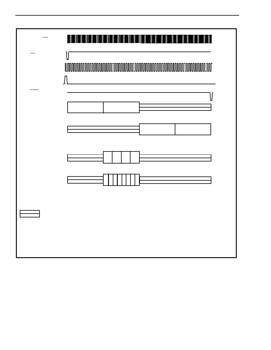
Figure 4 - SSI 8-Bit Companded PCM Relative Timing
Figure 5 - SSI 16-Bit Linear PCM Relative Timing
ADPCM i/o
BCLK
ENB1
ENB2/F0od
PCMi/o1
ADPCM i/o
SEL = 0
SEL = 1
32 kb/s
24 kb/s
16 kb/s
SEL for 16 kb/s only
B1
B2
PCMi/o2
1 2 3 4
B1
B2
1 2 3 x
B1
B2
1 2
B3
B4
1 2 1 2
1 2 1 2 1 2 1 2 1 2
7 6 5
3
4
2 1 0
B3
B4
1 2 3 4
1 2 3 x
1 2 3 4
B3
B4
1 2 3 x
1 2 3 4
1 2 3 x
B1
B2
B3
B4
7 6 5
3
4
2 1 0
7 6 5
3
4
2 1 0 7 6 5
3
4
2 1 0
X = undetermined logic level output; don't care input
Two frame delay from data input to data output
Outputs high impedance outside of channel strobe boundaries
ENB1
ENB2/F0od
EN1
ADPCM i/o
ADPCMi/o
B
1
1234 1234 1234 1234
123x 123x 123x 123x
12
SEL = 1
SEL = 1
SEL = 0
AA
AA
AA
AA
AA
BCLK
...
SEL for 16 kb/s only
(2.048 MHz only)
PCMi/o1
PCMi/o2
SSS 12 11 10 9 8 7 6 5 4 3 2 1 0
SSS 12 11 10 9 8 7 6 5 4 3 2 1 0
SSS 12 11 10 9 8 7 6 5 4 3 2 1 0
B1
B2
S = 3 bits sign extension
µ-
Law is 13 bit 2's complement data (bits 0 -12)
A-Law is 12 bit 2's complement data (shifted left once and utilizing
bits 1 - 12, bit 0 not defined)
32 kb/s
24 kb/s
16 kb/s
B3
B4
SSS 12 11 10 9 8 7 6 5 4 3 2 1 0
Notes:
B
2
B
3
B
4
12 12 12
B
1
12
B
2
B
3
B
4
12 12 12
B1
B2
B3
B4
1234 1234
123x 123x
B3
B4
B
1
12
B
2
B
3
B
4
12 12 12
X = undetermined logic level output; don't care input
Two frame delay from data input to data output
Outputs high impedance outside of channel strobe boundaries

MT9126
Preliminary Information
8-42
Figure 6 - SSI PCM and ADPCM Bypass Relative Timing
A
A
A
A
A
A
A
A
A
A
A
A
A
A
A
A
A
A
A
A
A
A
A
A
A
A
A
A
A
A
A
A
A
A
A
A
A
A
A
A
A
A
A
A
A
A
A
A
A
A
A
A
A
A
A
A
A
A
A
A
A
A
A
A
A
A
A
A
A
A
A
A
A
A
A
A
A
A
A
A
A
A
A
A
A
A
A
A
A
A
A
A
A
A
A
A
A
A
A
A
A
A
A
A
A
A
A
A
A
A
A
A
A
A
A
A
A
A
A
A
A
A
A
A
A
A
A
A
A
A
A
A
A
A
A
A
A
A
A
A
A
A
A
A
A
A
A
A
A
A
AA
AA
AA
AA
AA
AA
AA
AA
AA
AA
AA
AA
AA
AA
AA
AA
AA
AA
AA
AA
AA
AA
AA
AA
AA
AA
AA
AA
AA
AA
AA
AA
AA
AA
AA
AA
AA
AA
AA
AA
AA
AA
AA
AA
AA
AA
AA
AA
AA
AA
AA
AA
AA
AA
AA
AA
AA
AA
AA
AA
AA
AA
AA
AA
AA
AA
AA
AA
AA
AA
AA
AA
AA
AA
AA
AA
AA
AA
AA
AA
AA
AA
AA
AA
AA
AA
AA
AA
AA
AA
AA
AA
AA
AA
AA
AA
AA
AA
AA
AA
AA
AA
AA
AA
AA
AA
AA
AA
AA
AA
AA
AA
AA
AA
AA
AA
AA
AA
AA
AA
AA
AA
AA
AA
AA
AA
AA
AA
AA
AA
AA
AA
AA
AA
AA
AA
AA
AA
AA
AA
AA
AA
AA
AA
AA
AA
AA
AA
AA
AA
AA
AA
AA
AA
ADPCMo/i
BCLK
ENB1
ENB2/F0od
PCMi/o1
7 6 5
3
4
2 1 0
B1
B2
7 6 5
3
4
2 1 0
PCMi/o2
7 6 5
3
4
2 1 0
B3
B4
7 6 5
3
4
2 1 0
7 6 5
3
4
2 1 0
7 6 5
3
4
2 1 0
SEL = 0
ADPCMo/i
PCMi/o1
1 2 3
x
4
x x x
SEL = 1
B1
B2
PCMi/o2
B3
B4
SEL = 0
1 2 3
x
4
x x x
1 2 3
x
4
x x x
1 2 3 4 1 2 3 4 1 2 3 4 1 2 3 4
ADPCM o/i
PCMi/o1
PCMi/o2
1 2 x
x
x
x x x
B1
B2
B3
B4
1 2 x
x
x
x x x
1 2 x
x
x
x x x
1 2 x
x
x
x x x
1 2 1 2 1 2 1 2
1 2 1 2
1 2 1 2
B1
B2 B3
B4
B1
B2 B3
B4
32 kb/s using bits 1 2 3 4
24 kb/s where bit 4 = x
16 kb/s
SSI PCM
Bypass
SSI ADPCM
Bypass
SEL = 1
AA
AA
AA
AA
AA
AA
AA
AA
AA
AA
AA
AA
AA
AA
AA
AA
AA
AA
AA
AA
AA
AA
AA
AA
AA
AA
AA
AA
AA
AA
AA
AA
AA
AA
AA
AA
AA
AA
AA
AA
AA
AA
AA
AA
AA
AA
AA
AA
AA
AA
AA
AA
AA
AA
AA
AA
AA
AA
AA
AA
AA
AA
AA
AA
AA
AA
AA
AA
A
AA
AA
AA
AA
AA
AA
AA
AA
AA
AA
AA
AA
AA
AA
AA
A
AA
AA
AA
AA
AA
AA
AA
AA
AA
AA
AA
AA
AA
AA
AA
AA
AA
AA
AA
AA
AA
AA
AA
AA
AA
1 2 3
x
4
x x x
A
AA
AA
AA
AA
AA
AA
AA
AA
AA
AA
AA
AA
AA
X = undetermined logic level output; don't care input
Two frame delay from data input to data output
Outputs high impedance outside of channel strobe boundaries
Preliminary Information
MT9126
8-43
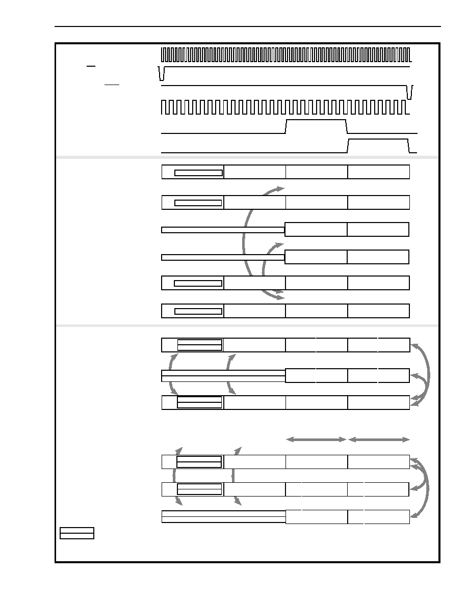
Figure 7 - ST-BUS 8-bit Companded PCM Relative Timing
MCLK (C4)
F0i
AA
AA
AA
AA
AA
AA
AA
AA
AA
AA
AA
AA
AA
AA
AA
AA
AA
AA
AA
AA
AA
AA
AA
AA
AA
AA
AA
AA
AA
AA
AA
AA
AA
AA
AA
AA
AA
AA
AA
AA
AA
AA
AA
AA
AA
AA
AA
AA
AA
AA
AA
AA
AA
AA
AA
AA
AA
AA
AA
AA
AA
AA
AA
AA
AA
AA
AA
AA
AA
AA
AA
AA
AA
AA
AA
AA
AA
AA
AA
AA
AA
AA
AA
AA
AA
AA
AA
AA
AA
AA
AA
AA
AA
AA
AA
AA
AA
AA
AA
AA
AA
AA
AA
AA
AA
AA
AA
AA
AA
AA
AA
AA
AA
AA
AA
AA
AA
AA
AA
AA
AA
AA
AA
AA
AA
AA
AA
AA
AA
AA
AA
AA
AA
AA
AA
AA
AA
AA
AA
AA
AA
AA
AA
AA
AA
AA
AA
AA
AA
AA
AA
AA
AA
AA
AA
AA
AA
AA
AA
AA
AA
AA
AA
AA
AA
AA
AA
AA
AA
AA
AA
AA
AA
AA
AA
AA
AA
AA
AA
AA
AA
AA
AA
AA
AA
AA
AA
AA
AA
AA
AA
AA
AA
AA
AA
AA
AA
AA
AA
AA
AA
AA
AA
AA
AA
AA
AA
AA
AA
AA
AA
AA
AA
AA
AA
AA
AA
AA
AA
AA
AA
AA
AA
AA
AA
AA
AA
AA
AA
AA
AA
AA
AA
AA
AA
AA
AA
AA
AA
AA
AA
AA
AA
AA
AA
AA
AA
AA
AA
AA
AA
AA
AA
AA
AA
AA
AA
AA
AA
AA
AA
AA
AA
AA
AA
AA
AA
AA
AA
AA
AA
AA
AA
AA
AA
AA
AA
AA
AA
AA
AA
AA
AA
AA
AA
AA
AA
AA
AA
AA
AA
AA
AA
AA
AA
AA
AA
AA
AA
AA
AA
AA
AA
AA
AA
AA
AA
AA
AA
AA
AA
AA
AA
AA
AA
AA
AA
AA
AA
AA
AA
AA
AA
AA
AA
AA
AA
AA
AA
AA
AA
AA
AA
AA
AA
AA
AA
AA
AA
AA
AA
AA
AA
AA
AA
AA
AA
AA
AA
AA
AA
AA
AA
AA
AA
AA
AA
AA
AA
AA
AA
AA
AA
AA
AA
AA
AA
AA
AA
AA
AA
AA
AA
AA
AA
AA
AA
AA
AA
AA
AA
AA
AA
AA
AA
AA
AA
AA
AA
AA
AA
AA
AA
AA
AA
AA
AA
AA
AA
AA
AA
AA
AA
AA
AA
AA
AA
AA
AA
AA
AA
AA
AA
AA
AA
AA
AA
AA
AA
AA
AA
AA
AA
AA
AA
AA
AA
AA
AA
AA
AA
AA
AA
AA
AA
AA
AA
AA
AA
AA
AA
AA
AA
AA
AA
AA
AA
AA
AA
AA
AA
AA
AA
AA
AA
AA
AA
AA
AA
AA
AA
AA
AA
AA
A
AA
AA
AA
AA
AA
AA
AA
AA
AA
AA
AA
AA
AA
AA
AA
AA
AA
AA
AA
AA
AA
AA
AA
AA
AA
AA
AA
AA
AA
AA
AA
AA
AA
AA
AA
AA
AA
AA
AA
AA
AA
AA
AA
AA
AA
AA
AA
AA
AA
AA
AA
AA
AA
AA
AA
AA
AA
AA
AA
AA
AA
AA
AA
AA
AA
AA
AA
AA
AA
AA
AA
AA
AA
AA
AA
AA
AA
AA
AA
AA
AA
AA
AA
AA
AA
AA
AA
AA
AA
AA
AA
AA
AA
AA
AA
AA
AA
AA
AA
AA
AA
AA
AA
AA
AA
AA
AA
AA
AA
AA
AA
AA
AA
AA
AA
AA
AA
AA
AA
AA
AA
AA
AA
AA
AA
ADPCMi
ADPCMo
C2o (output)
B1
B2
B3
B4
EN1 (output)
EN2 (output)
PCMi2
PCMo2
B3
B4
PCMi1
PCMo1
B1
B2
D
C
D
C
B1
SEL=0
SEL=1
B2
B4
B3
B1 B2
B4
B3
B1 B2
B4
B3
B1 B2
B4
B3
32 kb/s is shown
In 24 kb/s, bit 4 becomes "X"
16 kb/s
SEL operates for
ENB2/F0od
7 6 5 4
7 6 5 4 3 2 1 0
3 2 1 0
7 6 5 4
7 6 5 4 3 2 1 0
3 2 1 0
7 6 5 4
7 6 5 4 3 2 1 0
3 2 1 0
0 1
7 6 5 4 3 2 1 0
1 2 1 2 1 2 1 2 1 2 1 2 1 2 1 2
1 2 1 2 1 2 1 2 1 2 1 2 1 2 1 2
1 2 3 4
1 2 3 4 1 2 3 4
1 2 3 4
7 6 5 4
7 6 5 4 3 2 1 0
3 2 1 0
0 1
7 6 5 4 3 2 1 0
transparent relay of D- and C- channels
when ENB1=0
0 1
7 6 5 4 3 2 1 0
1 2 3 4
1 2 3 4 1 2 3 4
1 2 3 4
0 1
7 6 5 4 3 2 1 0
AA
AA
AA
AA
AA
AA
AA
AA
AA
AA
AA
AA
AA
AA
AA
AA
AA
AA
AA
AA
AA
AA
AA
AA
AA
AA
AA
AA
AA
AA
AA
AA
AA
AA
AA
AA
AA
AA
AAAA
AAAA
AAAA
AAAA
AAAA
AAAA
AAAA
AAAA
AAAA
AAAA
AAAA
AAAA
AAAA
AAAA
AAAA
AAAA
AAAA
AAAA
outputs=High impedance
inputs = don't care
AAAA
AAAA
AAAA
AAAA
AAAA
AAAA
AAAA
AAAA
AAAA
AAAA
AAAA
AAAA
A
A
A
AAAA
AAAA
AAAA
AAAA
AAAA
AAAA
AAAA
AAAA
AAAA
AAAA
AAAA
AAAA
A
A
A
AAAA
AAAA
AAAA
AAAA
AAAA
AAAA
AAAA
AAAA
AAAA
AAAA
AAAA
AAAA
A
A
A
AAAA
AAAA
AAAA
AAAA
AAAA
AAAA
AAAA
AAAA
AAAA
AAAA
AAAA
AAAA
A
A
A
AAAA
AAAA
AAAA
AAAA
AAAA
AAAA
AAAA
AAAA
AAAA
AAAA
AAAA
AAAA
AAAA
AAAA
AAAA
AAAA
AAAA
AAAA
AAAA
AAAA
AAAA
AAAA
AAAA
AAAA
AAAA
AAAA
AAAA
AAAA
AAAA
AAAA
AAAA
AAAA
AAAA
AAAA
AAAA
AAAA
AAAA
AAAA
AAAA
AAAA
AAAA
AAAA
AAAA
AAAA
AAAA
AAAA
AAAA
AAAA
AAAA
AAAA
AAAA
AAAA
AAAA
AAAA
AAAA
AAAA
AAAA
AAAA
AAAA
AAAA
AAAA
AAAA
AAAA
AAAA
AAAA
AAAA
X = undetermined logic level output; don't care input
Two frame delay from data input to data output
Outputs high impedance outside of channel boundaries
16 kb/s only
MT9126
Preliminary Information
8-44
Figure 8 - ST-BUS 16-bit Linear PCM Relative Timing
A
A
A
A
A
A
A
A
A
A
A
A
A
A
A
A
A
A
A
A
A
A
A
A
A
A
A
A
A
A
A
A
A
A
A
A
A
A
A
A
A
A
A
A
A
A
A
A
A
A
A
A
A
A
A
A
A
A
A
A
A
A
A
A
A
A
A
A
A
A
A
A
A
A
A
A
A
A
A
A
A
A
A
A
A
A
A
A
A
A
A
A
A
A
A
A
A
A
A
A
A
A
A
A
A
A
A
A
A
A
A
A
A
A
A
A
A
A
A
A
A
A
A
A
A
A
A
A
A
A
A
A
A
A
A
A
A
A
A
A
A
A
A
A
A
A
A
A
A
A
A
A
A
A
A
A
A
A
A
A
A
A
A
A
A
A
A
A
A
A
A
A
A
A
A
A
A
A
A
A
A
A
A
A
A
A
A
A
A
A
A
A
A
A
A
A
A
A
A
A
A
A
A
A
A
A
A
A
A
A
A
A
A
A
A
A
A
A
A
A
A
A
A
A
A
A
A
A
A
A
A
A
A
A
A
A
A
A
A
A
A
A
A
A
A
A
A
A
AA
AA
AA
AA
AA
AA
AA
AA
AA
AA
AA
AA
AA
AA
AA
AA
AA
AA
AA
AA
AA
AA
AA
AA
AA
AA
AA
AA
AA
AA
AA
AA
AA
AA
AA
AA
AA
AA
AA
AA
AA
AA
AA
AA
AA
AA
AA
AA
AA
AA
AA
AA
AA
AA
AA
AA
AA
AA
AA
AA
AA
AA
AA
AA
AA
AA
AA
AA
AA
AA
AA
AA
AA
AA
AA
AA
AA
AA
AA
AA
AA
AA
AA
AA
AA
AA
AA
AA
AA
AA
AA
AA
AA
AA
AA
A
A
A
A
A
A
A
A
A
A
A
A
A
A
A
A
A
A
A
A
A
A
A
A
A
A
A
A
A
A
A
A
A
A
A
A
A
A
A
A
A
A
A
A
A
A
A
A
A
A
A
A
A
A
A
A
A
A
A
A
A
A
A
A
A
A
A
A
A
A
A
A
A
A
A
A
A
A
A
A
A
A
A
A
A
A
A
A
A
A
A
A
A
A
A
A
A
A
A
MCLK (C4i)
F0i
C2o
ADPCMi/o
Note: D &C channels not supported in this mode.
SEL operated for
PCMi/o1
PCMi/o2
SSS 12 11 10 9 8 7 6 5 4 3 2 1 0
SSS 12 11 10 9 8 7 6 5 4 3 2 1 0
SSS 12 11 10 9 8 7 6 5 4 3 2 1 0
SSS 12 11 10 9 8 7 6 5 4 3 2 1 0
B1
B2
B3
B4
ADPCMi/o
(32/24 kb/s)
(16 kb/s)
F0od/ENB2
EN1 (output)
A
A
A
A
A
A
A
A
A
A
A
bit 4 = x at 24 kbit/s
B
1
12
SEL = 1
SEL = 0
B
2
B
3
B
4
12 12 12
B
1
12
B
2
B
3
B
4
12 12 12
1234 1234 1234 1234
B1
B2
B3
B4
16kb/s only
AA
AA
AA
AA
AA
AA
AA
AA
AA
AAAA
AAAA
AAAA
AAAA
AAAA
AAAA
AAAA
AAAA
AAAA
AAAA
AAAA
AAAA
AAAA
AAAA
AAAA
AAAA
AAAA
AAAA
outputs = High impedance
inputs = don't care
X = undetermined logic level output; don't care input
Two frame delay from data input to data output
Outputs high impedance outside of channel boundaries
AAAA
AAAA
AAAA
AAAA
AAAA
AAAA
AAAA
AAAA
AAAA
AAAA
AAAA
AAAA
AAAA
AAAA
AAAA
AAAA
AAAA
AAAA
AAAA
AAAA
AAAA
AAAA
AAAA
AAAA
AAAA
AAAA
AAAA
AAAA
AAAA
AAAA
AAA
AAA
AAA
AAAA
AAAA
AAAA
AAAA
AAAA
AAAA
AAAA
AAAA
AAAA
AAAA
AAAA
AAAA
AAAA
AAAA
AAAA
AAAA
AAAA
AAAA
AAAA
AAAA
AAAA
AAAA
AAAA
AAAA
AAAA
AAAA
AAAA
AAAA
AAAA
AAAA
AAA
AAA
AAA
AAAA
AAAA
AAAA
AAAA
AAAA
AAAA
AAAA
AAAA
AAAA
AAAA
AAAA
AAAA
AAAA
AAAA
AAAA
AAAA
AAAA
AAAA
AAAA
AAAA
AAAA
AAAA
AAAA
AAAA
AAAA
AAAA
AAAA
AAAA
AAAA
AAAA
AAAA
AAAA
AAAA
AAAA
AAAA
AAAA
AAAA
AAAA
AAAA
AAAA
AAAA
AAAA
AAAA
AAAA
AAAA
AAAA
AAAA
AAAA
AAAA
AAAA
AAAA
AAAA
AAAA
AAAA
AAAA
AAAA
AAAA
AAAA
AAAA
AAAA
AAAA
AAAA
AAAA
AAAA
AAAA
AAAA
AAAA
AAAA
AAAA
AAAA
AAAA
AAAA
AAAA
AAAA
AAAA
AAAA
AAAA
AAAA
AAAA
AAAA
AAAA
AAAA
AAAA
AAAA
AAAA
AAAA
AAAA
AAAA
AAAA
AAAA
AAAA
AAAA
AAAA
AAAA
AAAA
AAAA
AAA
AAA
AAA
AAAA
AAAA
AAAA
AAAA
AAAA
AAAA
AAAA
AAAA
AAAA
AAAA
AAAA
AAAA
AAAA
AAAA
AAAA
AAAA
AAAA
AAAA
AAAA
AAAA
AAAA
AAAA
AAAA
AAAA
AAAA
AAAA
AAAA
AAAA
AAAA
AAAA
AAA
AAA
AAA
AAAA
AAAA
AAAA
AAAA
AAAA
AAAA
AAAA
AAAA
AAAA
AAAA
AAAA
AAAA
AAAA
AAAA
AAAA
AA
AA
AA
AAAA
AAAA
AAAA
AAAA
AAAA
AAAA
AAAA
AAAA
AAAA
AAAA
AAAA
AAAA
AAAA
AAAA
AAAA
AA
AA
AA
AAAA
AAAA
AAAA
AAAA
AAAA
AAAA
AAAA
AAAA
AAAA
AAAA
AAAA
AAAA
AAAA
AAAA
AAAA
AAAA
AAAA
AAAA
AAAA
AAAA
AAAA
AAAA
AAAA
AAAA
AAAA
AAAA
AAAA
AAAA
AAAA
AAAA
AAA
AAA
AAA
AAAA
AAAA
AAAA
AAAA
AAAA
AAAA
AAAA
AAAA
AAAA
AAAA
AAAA
AAAA
AAAA
AAAA
AAAA
AAAA
AAAA
AAAA
AAAA
AAAA
AAAA
AAAA
AAAA
AAAA
AAAA
AAAA
AAAA
AAAA
AAAA
AAAA
AAA
AAA
AAA
AAAA
AAAA
AAAA
AAAA
AAAA
AAAA
AAAA
AAAA
AAAA
AAAA
AAAA
AAAA
AAAA
AAAA
AAAA
AAA
AAA
AAA
AAAA
AAAA
AAAA
AAAA
AAAA
AAAA
AAAA
AAAA
AAAA
AAAA
AAAA
AAAA
AAAA
AAAA
AAAA
AAA
AAA
AAA
Preliminary Information
MT9126
8-45
Figure 9 - ST-BUS PCM and ADPCM Bypass Relative Timing
A
A
A
A
A
A
A
A
A
A
A
A
A
A
A
A
A
A
A
A
A
A
A
A
A
A
A
A
A
A
A
A
A
A
A
A
A
A
A
A
A
A
A
A
A
A
A
A
A
A
A
A
A
A
A
A
A
A
A
A
A
A
A
A
A
A
A
A
A
A
A
A
A
A
A
A
A
A
A
A
A
A
A
A
A
A
A
A
A
A
A
A
A
A
A
A
A
A
A
A
A
A
A
A
A
A
A
A
A
A
A
A
A
A
A
A
A
A
A
A
A
A
A
A
A
A
A
A
A
A
A
A
A
A
A
A
A
A
A
A
A
A
A
A
A
A
A
A
A
A
A
A
A
A
A
A
A
A
A
A
A
A
A
A
A
A
A
A
A
A
A
A
A
A
A
A
A
A
A
A
A
A
A
A
A
A
A
A
A
A
A
A
A
A
A
A
A
A
A
A
A
A
A
A
A
A
A
A
A
A
A
A
A
A
A
A
A
A
A
A
A
A
A
A
A
A
A
A
A
A
A
A
A
A
A
A
A
A
A
A
A
A
A
A
A
A
A
A
A
A
A
A
A
A
A
A
A
A
A
A
A
A
A
A
A
A
A
A
A
A
A
A
A
A
A
A
A
A
A
A
A
A
A
A
A
A
A
A
A
A
A
A
A
A
A
A
A
A
A
A
A
A
A
A
A
A
A
A
A
A
A
A
A
A
A
A
A
A
A
A
A
A
A
A
A
A
A
A
A
A
A
A
A
A
A
A
A
A
A
A
A
A
A
A
A
A
A
A
A
A
A
A
A
A
A
A
A
A
A
A
A
A
A
A
A
A
A
A
A
A
A
A
A
A
A
A
A
A
A
A
A
A
A
A
A
A
A
A
A
A
A
A
A
A
A
A
A
A
A
A
A
A
A
A
A
A
A
A
A
A
A
A
A
A
A
A
A
A
A
A
A
A
A
A
A
A
A
A
A
A
A
A
A
A
A
A
A
A
A
A
A
A
A
A
A
A
A
A
A
A
A
A
A
A
A
A
A
A
A
A
A
A
A
A
A
A
A
A
A
A
A
A
A
A
A
A
A
A
A
A
A
A
A
A
A
A
A
A
A
A
A
A
A
A
A
A
A
A
A
A
A
A
A
A
A
A
AA
AA
A
AA
AA
AA
AA
AA
AA
AA
AA
AA
AA
AA
AA
AA
AA
AA
AA
AA
AA
AA
AA
AA
AA
AA
AA
AA
AA
AA
AA
AA
AA
AA
AA
AA
AA
AA
AA
AA
AA
AA
AA
AA
AA
AA
AA
AA
AA
AA
AA
AA
AA
AA
AA
AA
AA
AA
AA
AA
AA
AA
AA
AA
AA
AA
AA
AA
AA
AA
AA
AA
AA
AA
AA
AA
AA
AA
AA
AA
AA
AA
AA
AA
AA
AA
AA
AA
AA
AA
AA
AA
AA
AA
AA
AA
AA
AA
AA
AA
AA
AA
AA
AA
AA
AA
AA
AA
AA
AA
AA
AA
AA
AA
AA
AA
AA
AA
AA
AA
AA
AA
AA
AA
AA
AA
AA
AA
AA
AA
AA
AA
AA
AA
AA
AA
AA
AA
AA
AA
AA
AA
AA
AA
AA
AA
AA
AA
AA
AA
AA
AA
AA
AA
AA
AA
AA
AA
AA
AA
AA
AA
AA
AA
AA
AA
AA
AA
AA
AA
AA
AA
A
AA
AA
AA
AA
AA
AA
AA
AA
AA
AA
AA
AA
AA
AA
AA
AA
AA
AA
AA
AA
AA
AA
AA
AA
AA
AA
AA
AA
AA
AA
AA
AA
AA
AA
AA
AA
AA
AA
AA
AA
AA
AA
AA
AA
AA
AA
AA
AA
AA
AA
AA
AA
AA
AA
AA
AA
AA
AA
AA
AA
AA
AA
AA
AA
AA
AA
AA
AA
AA
AA
AA
AA
AA
AA
AA
AA
AA
AA
AA
AA
AA
AA
AA
AA
AA
AA
AA
AA
AA
AA
AA
AA
AA
AA
AA
AA
AA
AA
AA
AA
AA
AA
AA
AA
AA
AA
AA
AA
AA
AA
AA
AA
AA
AA
AA
AA
AA
AA
AA
AA
AA
AA
AA
AA
AA
AA
AA
AA
AA
AA
AA
AA
AA
AA
AA
AA
AA
AA
AA
AA
AA
AA
AA
AA
AA
AA
AA
AA
AA
AA
AA
AA
AA
AA
AA
AA
AA
AA
AA
AA
AA
AA
AA
AA
AA
AA
AA
EN1 (output)
EN2 (output)
MCLK
F0i
C2o
ADPCMi
ADPCMo
SEL=0
SEL=1
PCMi1
PCMo1
B1
B2
D
C
PCMi2
PCMo2
B3
B4
B1/B3
B2/B4
D
C
ADPCMi/o
ADPCMi/o
B3
B4
PCMi/o1
PCMi/o2
D
C
B1
B2
D
C
B3
B4
B1
B2
32 kb/s
24 kb/s bit 4 = X
(16 kb/s)
PCMi/o1
PCMi/o2
D
C
B1
SEL=0
SEL=1
B2 B4
B3
B3
B4
C
D
x x x x
B2
B1
0 1
0 1
0 1
P
C
M
B
y
p
a
s
s
A
D
P
C
M
B
y
p
a
s
s
x x x x
AA
AA
A
AA
AA
AA
AA
AA
AA
AA
AA
AA
AA
AA
AA
AA
AA
AA
AA
AA
AA
AA
AA
AA
AA
AA
AA
AA
AA
AA
AA
AA
AA
AA
AA
AA
AA
AA
AA
AA
AA
AA
AA
AA
A
A
A
A
A
A
A
A
A
A
A
A
A
A
A
A
A
A
A
A
A
A
A
A
AA
AA
AA
AA
AA
AA
AA
AA
AA
AA
AA
AA
AAAA
AAAA
AAAA
AAAA
AAAA
AAAA
AAAA
AAAA
AAAA
AAAA
AAAA
AAAA
AAAA
AAAA
AAAA
AAAA
AAAA
AAAA
AAAA
AAAA
AAAA
AAAA
AAAA
AAAA
AAAA
AAAA
AAAA
AAAA
AAAA
AAAA
AAAA
AAAA
AAAA
AAAA
AAAA
AAAA
AAAA
AAAA
AAAA
AAAA
AAAA
AAAA
AAAA
AAAA
AAAA
AAAA
AAAA
AAAA
AAAA
AAAA
AAAA
AAAA
AAAA
AAAA
AAAA
AAAA
AAAA
AAAA
AAAA
AAAA
AAAA
AAAA
AAAA
AAAA
AAAA
AAAA
AAAA
AAAA
AAAA
AAAA
AAAA
AAAA
AAAA
AAAA
AAAA
AAAA
AAAA
AAAA
AAAA
AAAA
AAAA
AAAA
AAAA
AAAA
AAAA
AAAA
AAAA
AAAA
AAAA
AAAA
AAAA
AAAA
AAAA
AAAA
AAAA
AAAA
0 1
7 6 5 4 3 2 1 0
7 6 5 4 3 2 1 0
7 6 5 4 3 2 1 0
7 6 5 4 3 2 1 0
1 2 3 4
1 2 3 4
1 2 3 4 1 2 3 4
1 2 3 4 1 2 3 4
1 2 1 2 1 2 1 2
1 2 1 2 1 2 1 2
1 2 x x x x x x
B1
B2 B4
B3
1 2 x x x x x x
1 2 x x x x x x
1 2 x x x x x x
AA
AA
AA
AA
AA
AA
AA
AA
AA
AA
AA
AA
1 2 3 4
x x x x
1 2 3 4
x x x x
7 6 5 4 3 2 1 0
7 6 5 4 3 2 1 0
7 6 5 4 3 2 1 0
7 6 5 4 3 2 1 0
0 1
7 6 5 4 3 2 1 0
7 6 5 4 3 2 1 0
7 6 5 4 3 2 1 0
0 1
7 6 5 4 3 2 1 0
7 6 5 4 3 2 1 0
7 6 5 4 3 2 1 0
0 1
7 6 5 4 3 2 1 0
7 6 5 4 3 2 1 0
7 6 5 4 3 2 1 0
0 1
7 6 5 4 3 2 1 0
7 6 5 4 3 2 1 0
7 6 5 4 3 2 1 0
AAAA
AAAA
AAAA
AAAA
AAAA
AAAA
AAAA
AAAA
AAAA
A
A
A
AAAA
AAAA
AAAA
AAAA
AAAA
AAAA
AAAA
AAAA
AAAA
A
A
A
outputs = High impedance
inputs = don't care
X = undetermined logic level output; don't care input
Two frame delay from data input to data output
Outputs high impedance outside of channel boundaries
ENB2/F0od
AAAA
AAAA
AAAA
AAAA
AAAA
AAAA
AAAA
AAAA
AAAA
AAAA
AAAA
AAAA
AAAA
AAAA
AAAA
AAAA
AAAA
AAAA
AAAA
AAAA
AAAA
AAAA
AAAA
AAAA
AAAA
AAAA
AAAA
AAAA
AAAA
AAAA
AAA
AAA
AAA
AAAA
AAAA
AAAA
AAAA
AAAA
AAAA
AAAA
AAAA
AAAA
AAAA
AAAA
AAAA
AAAA
AAAA
AAAA
AAAA
AAAA
AAAA
AAAA
AAAA
AAAA
AAAA
AAAA
AAAA
AAAA
AAAA
AAAA
AAAA
AAAA
AAAA
AAA
AAA
AAA
AAAA
AAAA
AAAA
AAAA
AAAA
AAAA
AAAA
AAAA
AAAA
AAAA
AAAA
AAAA
AAAA
AAAA
AAAA
AAAA
AAAA
AAAA
AAAA
AAAA
AAAA
AAAA
AAAA
AAAA
AAAA
AAAA
AAAA
AAAA
AAAA
AAAA
AAA
AAA
AAA
AAAA
AAAA
AAAA
AAAA
AAAA
AAAA
AAAA
AAAA
AAAA
AAAA
AAAA
AAAA
AAAA
AAAA
AAAA
AAAA
AAAA
AAAA
AAAA
AAAA
AAAA
AAAA
AAAA
AAAA
AAAA
AAAA
AAAA
AAAA
AAAA
AAAA
AAA
AAA
AAA
AAAA
AAAA
AAAA
AAAA
AAAA
AAAA
AAAA
AAAA
AAAA
AAAA
AAAA
AAAA
AA
AA
AA
AAAA
AAAA
AAAA
AAAA
AAAA
AAAA
AAAA
AAAA
AAAA
AAAA
AAAA
AAAA
AA
AA
AA
AAAA
AAAA
AAAA
AAAA
AAAA
AAAA
AAAA
AAAA
AAAA
AAAA
AAAA
AAAA
AAAA
AAAA
AAAA
AAAA
AAAA
AAAA
AAAA
AAAA
AAAA
AAAA
AAAA
AAAA
AAAA
AAAA
AAAA
AAAA
AAAA
AAAA
AAA
AAA
AAA
AAAA
AAAA
AAAA
AAAA
AAAA
AAAA
AAAA
AAAA
AAAA
AAAA
AAAA
AAAA
AAAA
AAAA
AAAA
AAAA
AAAA
AAAA
AAAA
AAAA
AAAA
AAAA
AAAA
AAAA
AAAA
AAAA
AAAA
AAAA
AAAA
AAAA
AAA
AAA
AAA
AAAA
AAAA
AAAA
AAAA
AAAA
AAAA
AAAA
AAAA
AAAA
AAAA
AAAA
AAAA
AA
AA
AA
AAAA
AAAA
AAAA
AAAA
AAAA
AAAA
AAAA
AAAA
AAAA
AAAA
AAAA
AAAA
A
A
A
MT9126
Preliminary Information
8-46
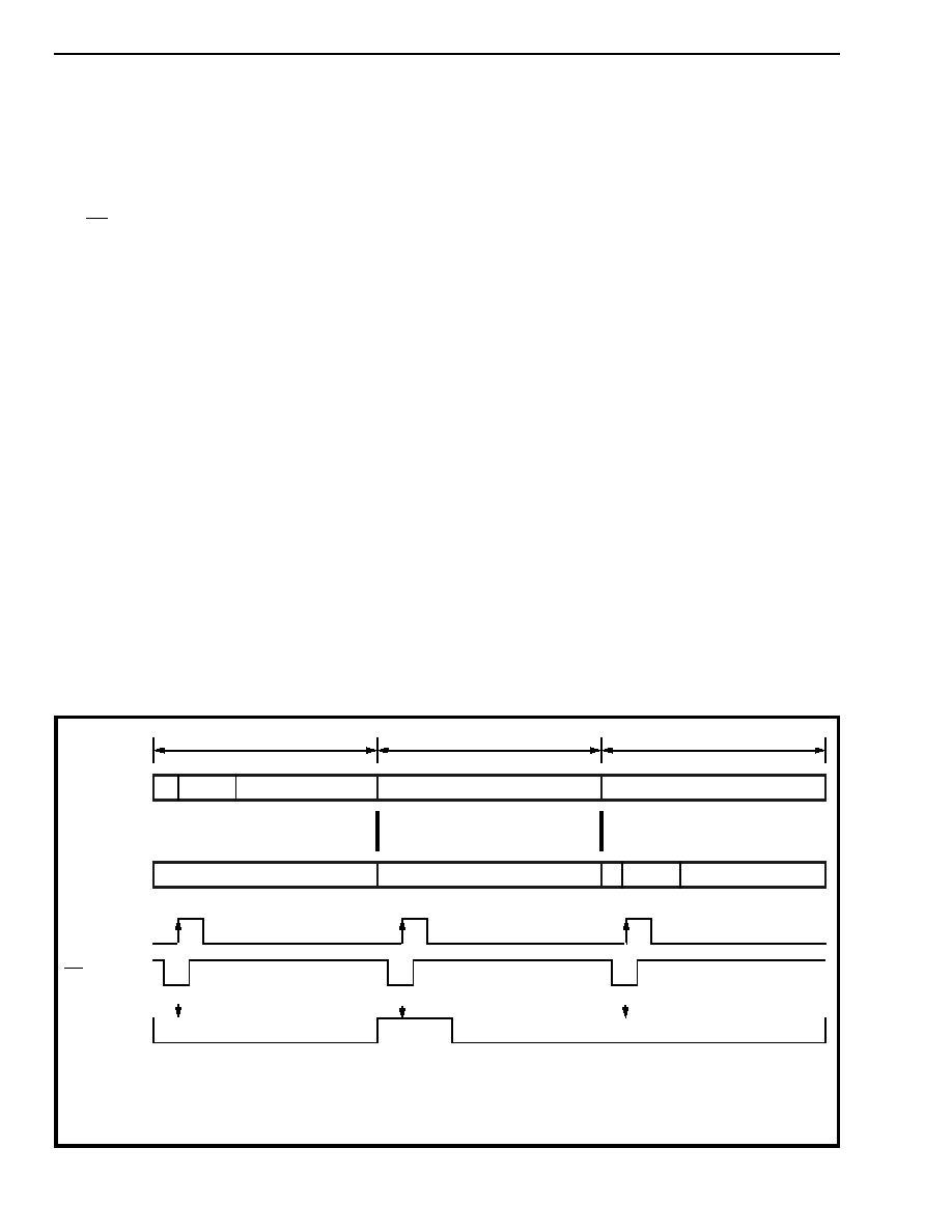
Figure 10 - Data Throughput
AA
AA
AA
A
A
A
A
A
A
A
A
A
A
A
A
A
A
PCMi1/2
ADPCMo
ENB1 or ENB2
F0i
MS1 or 4
Where MS2, 3, 5, 6 = 0
frame n-1
frame n
frame n+1
PCM Byte "X" latched into device
during frame n-1
PCM Byte "X" processed according
to MSn input states latched during
frame n
ADPCM Word "X" output from
device during frame n+1
32 kb/s
24 kb/s
32 kb/s
This diagram shows the conversion sequence from PCM to ADPCM. The same pipelining occurs in the
reverse ADPCM to PCM direction.
Total delay from data input to data output = 2 frames.
AA
AA
AA
AA
AA
AA
AA
AA
AA
AA
AA
AA
AA
AA
AA
AA
AA
AA
AA
AA
AA
AA
AA
AA
AA
AA
AA
AA
AA
AA
AA
AA
AA
AA
AA
Byte "x"
Word "x"
Processing Delay Through the Device
In order to accommodate variable rate PCM and
ADPCM interfaces, the serial input and output
streams require a complete frame to load internal
shift registers. Internal frame alignment of the
encoding/decoding functions are taken from either of
the F0i or ENB1 & ENB2 input strobes depending
upon the device operating mode (i.e., ST-BUS or
SSI). The encoding/decoding of all channels then
takes one frame to complete before the output
buffers are loaded. This results in a two frame
transcoding delay. The two frame delay also applies
to the D and C channels and to the PCM and
ADPCM bypass functions.(See Figure 10.)
Note: When changing the relative positions of the
ENB1 and ENB2 strobes, precaution must be taken
to ensure that two conditions are met. They are:
1)
There must be at least 512 master clock cycles
between consecutive rising edges of ENB1. This
condition also holds true for ENB2.
2)
The ENB1 strobe must alternate with the ENB2
strobe.
Violation of these requirements may cause noise on
the output channels.
Applications
Figure 11 depicts an ISDN line card utilizing the
MT8910 'U' interface transciever and MT9126
ADPCM transcoder. This central office application
implements the network end of a Pair-Gain system.
Figure 12 shows Mitel devices used to construct the
remote Pair-Gain loop terminator.
Figure 13 depicts an ADPCM to linear PCM
converter for applications where further, value
added, functions are being performed via digital
signal processor. Access to linear coded PCM
reduces the overhead of the DSP by removing the
need for a companded to linear conversion. The
linear PCM capability of the ADPCM transcoder in
conjunction with the frame alignment signal EN1
allows direct connection to the serial port of both
Motorola and Texas Instruments Digital Signal
Processors. Daisy-chaining via the delayed frame
strobe output ensures that the ADPCM array is
distributed over the complete 2048 kbit bandwidth. If
the DSP has a second serial port then access to the
processed PCM can be had directly. For processors
with only one serial port the MT8920 connected to
the DSP parallel port will provide serial access by
parallel to serial conversion. The same daisy-
chained arrangement of Quad ADPCM transcoders
will provide a general system resource for PCM-
ADPCM conversion by setting the device to non-
linear operation.

Preliminary Information
MT9126
8-47
Figure 11 - ISDN Line Card with 32 kbit/s ADPCM
LIN-
F0b
C4b
F0od
DSTo
DSTi
MT8910
LIN+
LOUT+
LOUT-
MT8980
DX
ST1o
ST1i
C4i
F0i
F0i
F0od
C4i
A
A
AAAA
AAAA
AAAA
AAAA
AAAA
AAAA
AAAA
AAAA
AAAA
AAAA
AAAA
AAAA
AAAA
AAAA
AAAA
AAAA
AAAA
AAAA
AAAA
AAAA
AAAA
AAAA
AAAA
AAAA
AAAA
AAAA
AAAA
AAAA
AAAA
AAAA
AAAA
AAAA
AAAA
AAAA
AAAA
AAAA
AAAA
AAAA
AAAA
AAAA
AAAA
AAAA
AAAA
AAAA
AAAA
AAAA
AAAA
AAAA
AAAA
AAAA
AAAA
AAAA
AAAA
AAAA
AAAA
AAAA
AAAA
AAAA
AAAA
AAAA
A
A
A
A
A
A
A
A
A
A
A
A
A
A
A
A
A
A
A
A
AA
A
AAAA
AAAA
AAAA
AAAA
AAAA
AAAA
AAAA
AAAA
AAAA
AAAA
AAAA
AAAA
AAAA
AAAA
AAAA
AAAA
AAAA
AAAA
AAAA
AAAA
AAAA
AAAA
AAAA
AAAA
AAAA
AAAA
AAAA
AAAA
AAAA
AAAA
AAAA
AAAA
AAAA
AAAA
AAAA
AAAA
AAAA
AAAA
AAAA
AAAA
AAAA
AAAA
AAAA
AAAA
AAAA
AAAA
AAAA
AAAA
AAAA
AAAA
AAAA
AAAA
AAAA
AAAA
AAAA
AAAA
AAAA
AAAA
AAAA
AAAA
AAAA
AAAA
AAAA
AAAA
AAAA
AAAA
AAAA
AAAA
AAAA
AAAA
AAAA
AAAA
AAAA
AAAA
AAAA
AAAA
AAAA
AAAA
AAAA
AAAA
AAAA
AAAA
AAAA
AAAA
AAAA
AAAA
AAAA
AAAA
AAAA
AAAA
AAAA
AAAA
AAAA
AAAA
AAAA
AAAA
AAAA
AAAA
AAAA
AAAA
AAAA
AAAA
AAAA
AAAA
AAAA
AAAA
AAAA
AAAA
AAAA
AAAA
AAAA
AAAA
AAAA
AAAA
AAAA
AAAA
AAAA
AAAA
AAAA
AAAA
AAAA
AAAA
AAAA
AAAA
AAAA
AAAA
AAAA
AAAA
AAAA
AAAA
AAAA
AAAA
AAAA
AAAA
AAAA
AAAA
AAAA
AAAA
AAAA
AAAA
AAAA
AAAA
AAAA
AAAA
AAAA
AAAA
AAAA
AAAA
AAAA
AAAA
AAAA
AAAA
AAAA
AAAA
AAAA
AAAA
AAAA
AAAA
AAAA
AAAA
AAAA
AAAA
AAAA
AAAA
AAAA
AAAA
AAAA
AAAA
AAAA
AAAA
AAAA
AAAA
AAAA
AAAA
AAAA
AAAA
AAAA
AAAA
AAAA
AAAA
AAAA
AAAA
AAAA
AAAA
AAAA
AAAA
AAAA
AAAA
AAAA
AAAA
AAAA
AAAA
AAAA
AAAA
AAAA
AAAA
AAAA
AAAA
AAAA
AAAA
AAAA
AAAA
AAAA
AAAA
AAAA
AAAA
AAAA
AAAA
AAAA
AAAA
AAAA
AAAA
AAAA
AAAA
AAAA
AAAA
AAAA
AAAA
AAAA
AAAA
AAAA
AAAA
AAAA
AAAA
AAAA
AAAA
AAAA
AAAA
AAAA
AAAA
AAAA
AAAA
AAAA
AAAA
AAAA
AAAA
AAAA
AAAA
AAAA
AAAA
AAAA
AAAA
AAAA
AAAA
AAAA
AAAA
AAAA
AAAA
AAAA
AAAA
AAAA
AAAA
AAAA
AAAA
AAAA
AAAA
AAAA
AAAA
AAAA
AAAA
AAAA
AAAA
AAAA
AAAA
AAAA
AAAA
AAAA
AAAA
AAAA
AAAA
AAAA
AAAA
AAAA
AAAA
AAAA
AAAA
AAAA
AAAA
AAAA
AAAA
AAAA
AAAA
AAAA
AAAA
AAAA
AAAA
AAAA
AAAA
AAAA
AAAA
AAAA
AAAA
AAAA
AAAA
AAAA
AAAA
AAAA
AAAA
AAAA
AAAA
AAAA
AAAA
AAAA
AAAA
AAAA
AAAA
AAAA
AAAA
AAAA
AAAA
AAAA
AAAA
AAAA
AAAA
AAAA
AAAA
AAAA
AAAA
AAAA
AAAA
AAA
AAA
AAA
AAA
AAA
AAA
AAA
AAA
AAA
AAA
AAA
AAA
AAA
AAA
AAA
AAA
AAA
AAA
AAA
AAA
AAAAAAAAAAAAAAAAAAAAAAAAAAAAAAAAAAAAAAAAAAAAAAAAAAAAAAAAAAAAAAAAAAAAAAAAAAAAAAAAAAAAAAAAAAAAA
A
A
A
A
A
A
A
A
A
A
A
A
A
A
A
A
A
A
A
A
A
A
A
A
A
A
A
A
A
A
A
A
A
A
A
A
A
A
A
A
A
A
A
A
A
A
A
A
A
A
A
A
A
A
A
A
A
AAAAAAAAAAAAAAAAAAAAAAAAAAAAAAAAAAAAAAAAAAAAAAAAAAAAAAAAAAAAAAAAAAAAAAAAAAAAAAAAAAAAAAAAAAAAA
AA
AA
AA
AA
AA
AA
AA
AA
AA
AA
AA
AA
AA
AA
AA
AA
AA
AA
AA
AA
AA
AA
AA
AA
AA
AA
AA
AA
AA
AA
AA
AA
AA
AA
AA
AA
AA
AA
AA
AA
AA
AA
AA
AA
AA
AA
AA
AA
AA
AA
AA
AA
AA
AA
AA
AA
AA
1
2
8
PC
M
i
1
PC
M
o
2
F0i
F0od
C4i
ADPCMi
ADPCMo
PCMi1
PCMo1
MCLK
F0i
MT9126
PCMi2
PCMo2
ST2o
ST2i
PC
M
i
2
PC
M
o
1
PC
M
i
1
PC
M
o
2
F0i
F0od
C4i
PC
M
i
2
PC
M
o
1
PC
M
i
1
PC
M
o
2
F0i
F0od
C4
i
PC
M
i
2
PC
M
o
1
T
R
2
T R
1
T R
8
C4i
F0i
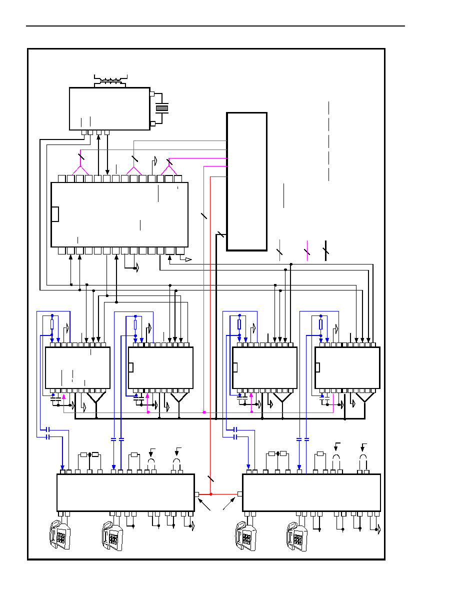
MT9126
Preliminary Information
8-48
1 2
3
4 5
6
7
8
9
10
11
12
13
14
15
16
20
19
18
17
1 2
3
4 5
6
7
8
9
10
11
12
13
14
15
16
20
19
18
17
1 2
3
4 5
6
7
8
9
10
11
12
13
14
15
16
20
19
18
17
VB
ia
s
VR
e
f
PW
R
S
T
IC
A/
µ
/IRQ
VS
SD
CS
SC
L
K
DA
T
A
1
DA
T
A
2
Do
ut
Di
n
ST
B/
F
0
i
CLO
C
K
i
n
VD
D
HS
P
K
R-
M+
M-
V
SSA
H
S
PKR
+
15
16
24
23
22
21
20
19
18
17
28
27
26
25
MT
89
72
M
T
89
10
5V
5V
5V
5V
8
or
MT
91
26
M
T
9
160
M
T
9
160
MT
9160
MT
9160
5V
3
3
3
16
Se
r
i
al
M
i
cr
o-
po
r
t
In
te
l M
C
S
-
5
1
Mot
o
r
o
l
a
SPI
Na
t
Se
mi
Mi
c
r
o
w
i
r
e
St
at
i
c
Con
t
r
o
l
:
SL
I
C
Funct
i
ons
O
p
t
i
onal
Q
A
DPCM
f
unc
t
i
onal
cont
r
o
l
M
i
c
r
oCont
rol
l
e
r
1
DS
T
o
DS
T
i
F0
b
C4
b
-5
V
5V
-2
4
V
DC
m
e
ter
s
i
gna
l
I/
P
m
e
ter
s
i
gnal
I/
P
12
0V
DC r
i
n
g
vo
l
t
a
g
e
120V
DC r
i
ng
v
o
l
t
age
1
6
co
n
t
r
o
l
/
s
t
atu
s
li
n
e
s
ar
e:
L
R
1/2,
E
S
E
1
/2,
S
HK1/
2
,
RC
1/2 - 8
x
2 S
L
IC
'
s
9
c
ont
rol li
ne
s
for QADP
C
M
,
s
o
m
e
o
p
ti
ona
l
8
s
i
g
n
a
l
s
for
m
i
c
r
opor
t
a
r
e
:
DA
T
A
1,
DA
T
A
2,
SC
L
K
,
IR
Q
, C
S
1
, CS
2
, C
S
3
, C
S
4
D-Cha
nne
l a
c
c
e
s
s
th
rough CODE
C1 Mic
r
oport
a
s
we
ll a
s
C-
Cha
nne
l
c
ont
rol
of
MT
8910/
MT
89
72
16
3
8
1
2
3
4
Re
s
e
t
TI
P
1
RING
1
DCRI
DCRI
VD
D
VD
D
V
BAT
VE
E
ESI
2
GN
D
VE
E
RING
2
TI
P
2
V
BAT
GN
D
VR
2
VX1
VR
1
VX2
ES
T
i
RF
1
RF
2
RF
3
RG
1
RG
2
4
37
34
28
11
13
30
7
18
19
20
21
22
1
2
14
27
3
25
26
16
39
40
38
15
Pi
n
s
MH8862
2
5V
-5
V
-2
4
V
DC
5,
8,
9
,
1
7
,
2
3
,
32
,
3
3,
3
6
10
.
24 MH
z
P
a
ir
G
a
in
S
L
IC
1
MH88
622
P
a
ir
G
a
in
S
L
IC 2
PC
M
o
1
BC
L
K
PC
M
i
1
LINE
A
R
EN
B
2
/
F
0
o
d
VS
S
C2o
MC
LK
F0
i
PC
M
i
2
EN
B
1
PC
M
o
2
EN
1
SE
L
1
2
3
4
5
6
7
8
9
10
11
12
13
14
MS
1
VD
D
MS
3
IC
MS
4
FO
R
M
A
T
MS
2
P
W
RDN
AD
P
C
M
i
AD
PC
M
o
MS
6
EN
2
A/
µ
MS
5
F
i
g
u
r
e
1
2
-
P
a
i
r
G
a
in
Re
mo
t
e
T
e
r
m
in
a
l
u
t
i
l
zi
n
g
M
i
t
e
l
Co
mp
o
n
e
n
t
s
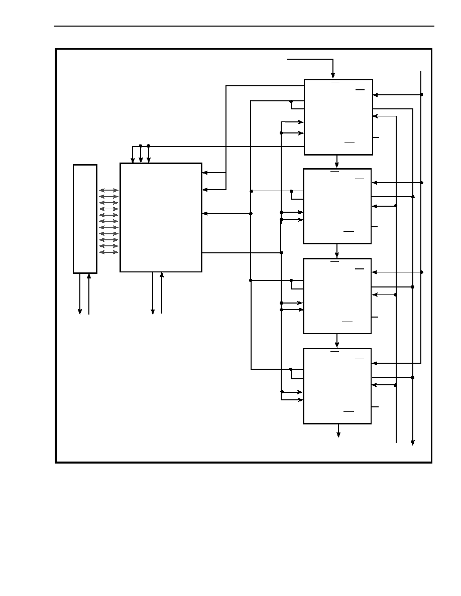
Preliminary Information
MT9126
8-49
Figure 13 - ST-BUS to DSP Platform
CLKR
CLKX
F
S
R
F
S
X
I
R
Q
0
DR
DX
System Frame pulse
System 4.096MHz
S
T
P
A
2nd serial port
if available
STPA
port
ADPCM BUS
TI DSP
C2o F0i
MCLK (C4i)
PCMo1
PCMo2 ADPCMo
ADPCMi
PCMi1
PCMi2
LINEAR
EN1 ENB2/F0od
C2o F0i
MCLK (C4i)
PCMo1
PCMo2 ADPCMo
ADPCMi
PCMi1
PCmi2
LINEAR
EN1 ENB2/F0od
C2o F0i
MCLK (C4i)
PCMo1
PCmo2 ADPCMo
ADPCMi
PCMi1
PCMi2
LINEAR
EN1 ENB2/F0od
C2o F0i
MCLK (C4i)
PCMo1
PCMo2 ADPCMo
ADPCMi
PCMi1
PCMi2
LINEAR
EN1 ENB2/F0od
MT9126
MT9126
MT9126
MT9126
+5v
+5v
+5v
+5v
ST-BUS
MT8920

MT9126
Preliminary Information
8-50
* Exceeding these values may cause permanent damage. Functional operation under these conditions is not implied.
Typical figures are at 25∞C and are for design aid only: not guaranteed and not subject to production testing.
Typical figures are at 25∞C and are for design aid only: not guaranteed and not subject to production testing.
* DC Electrical Characteristics are over recommended temperature and supply voltage.
Absolute Maximum Ratings*
Parameter
Symbol
Min
Max
Units
1
Supply Voltage
V
DD
-V
SS
-0.3
7.0
V
2
Voltage on any I/O pin
V
i
| V
o
V
SS
-0.3
V
DD
+ 0.3
V
3
Continuous Current on any I/O pin
I
i
| I
o
±20
mA
4
Storage Temperature
T
ST
-65
150
∞C
5
Package Power Dissipation
P
D
500
mW
Recommended Operating Conditions
- Voltages are with respect to ground (V
SS
) unless otherwise stated.
Characteristics
Sym
Min
Typ
Max
Units
Test Conditions
1
Supply Voltage
V
DD
4.5
5.0
5.5
V
2
TTL Input High Voltage
2.4
V
DD
V
400mV noise margin
3
TTL Input Low Voltage
V
SS
0.4
V
400mV noise margin
4
CMOS Input High Voltage
4.5
V
DD
V
5
CMOS Input Low Voltage
V
SS
0.5
V
6
Operating Temperature
T
A
-40
+85
∞C
DC Electrical Characteristics
- Voltages are with respect to ground (V
SS
) unless otherwise stated.
Characteristics
Sym
Min
Typ
Max
Units
Test Conditions
1
Supply Current
I
CC
I
DD
5
100
µ
A
mA
PWRDN = 0
PWRDN
= 1, clocks active
2
Input HIGH voltage (TTL)
V
IH
2.0
V
3
Input LOW voltage (TTL)
V
IL
0.8
V
4
M
C
L
K
Input HIGH voltage (CMOS)
V
IHC
3.5
V
5
Input LOW voltage (CMOS)
V
ILC
1.5
V
6
Input leakage current
I
IH
/I
IL
0.1
10
µ
A
V
IN
=V
SS
to V
DD
7
High level output voltage
V
OH
2.4
V
I
OL
=5.0mA
8
Low level output voltage
V
OL
0.4
V
I
OL
=5.0mA
9
High impedance leakage
I
OZ
1
10
µ
A
V
IN
=V
SS
to V
DD
10
Output capacitance
C
o
10
pF
11
Input capacitance
C
i
8
pF
12
P
W
R
D
N
Positive Threshold Voltage
Hysteresis
Negative Threshold Voltage
V+
V
H
V-
3.7
1.0
1.3
V
V
V

Preliminary Information
MT9126
8-51
Timing is over recommended temperature & power supply voltages.
Typical figures are at 25∞C and are for design aid only: not guaranteed and not subject to production testing.
AC Electrical Characteristics
- Serial PCM/ADPCM Interfaces (see Figure 14)
Voltages are with respect to ground (V
SS
) unless otherwise stated.
Characteristics
Sym
Min
Typ
Max
Units
Test Conditions
1
BCLK Clock High
t
BCH
80
ns
2
BCLK Clock Low
t
BCL
80
ns
3
BCLK Period
t
BCP
200
7900
ns
4
Data Output Delay (excluding first
bit)
t
DD
60
ns
C
L
=150pF//R
L
=1K
5
Output Active to High Z
t
AHZ
60
ns
C
L
=150pF//R
L
=1K
6
Strobe Signal Setup
t
SSS
80
t
BCL
-
80
ns
7
Strobe Signal Hold
t
SSH
80
t
BCL
-
80
ns
8
Data Input Setup
t
DIS
50
ns
9
Data Input Hold
t
DIH
50
ns
10
Strobe to Data Delay (first bit)
t
SD
60
ns
C
L
=150pF//R
L
=1K
11
F0i
Setup
t
F0iS
50
122
150
ns
12
F0i
Hold
t
F0iH
50
122
150
ns
13
MCLK (C4i) duty cycle
t
H
/t
L
x100
40
50
60
%
14
F0od Delay
t
DFD
60
ns
C
L
=150pF//R
L
=1K
15
F0od Pulse Width
t
DFW
244
ns
C
L
=150pF//R
L
=1K
16
MCLK (C4i) period
t
C4P
61
244.2
ns
17
Data Output delay
t
DSD
95
ns
C
L
=150pF//R
L
=1K
18
Data in Hold time
t
DSH
50
ns
19
Data in Setup time
t
DSS
50
ns
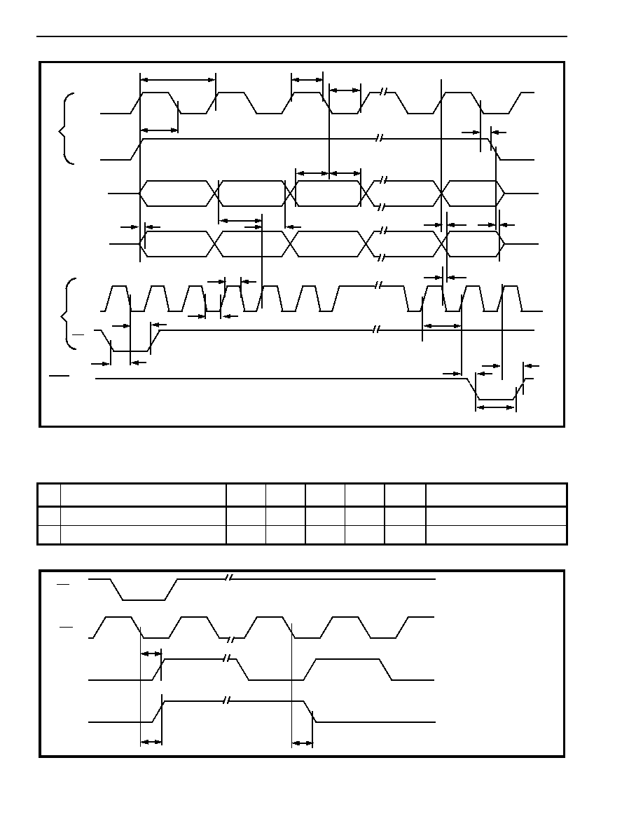
MT9126
Preliminary Information
8-52
Figure 14 - Serial Port Timing
Figure 15 - ST-BUS Timing for External Signal Generation
AC Electrical Characteristics
- ST-BUS C2o Conversion
Voltages are with respect to ground (V
SS
) unless otherwise stated.
Characteristics
Sym
Min
Typ
Max
Units
Test Conditions
1
Delay MCLK falling to C2o rising
t
D1
100
ns
150pF//1K Load
2
Delay MCLK falling to Enable
t
D2
100
ns
150pF//1K Load
A
A
A
A
AAAA
AAAA
AAAA
AAAA
AAAA
AAAA
AAAA
AAAA
AAAA
AAAA
AAAA
AAAA
AAAA
AAAA
AAAA
AAAA
AAAA
AAAA
AAAA
AAAA
AAAA
AAAA
AAAA
AAAA
AAAA
AAAA
AAAA
AAAA
AAAA
AAAA
AAAA
AAAA
AAAA
AAAA
AAAA
AAAA
AAAA
AAAA
AAAA
AAAA
AAAA
AAAA
AAAA
AAAA
AAAA
AAAA
AAAA
AAAA
AAAA
AAAA
AAAA
AAAA
AAA
AAA
A
A
A
A
AAAA
AAAA
AAAA
AAAA
AAAA
AAAA
AAAA
AAAA
AAAA
AAAA
AAAA
AAAA
AAAA
AAAA
AAAA
AAAA
AAAA
AAAA
AAAA
AAAA
AAAA
AAAA
AAAA
AAAA
AAAA
AAAA
AAAA
AAAA
AAAA
AAAA
AAAA
AAAA
AAAA
AAAA
AAAA
AAAA
AAAA
AAAA
AAAA
AAAA
AAAA
AAAA
AAAA
AAAA
AAAA
AAAA
AAAA
AAAA
AAAA
AAAA
AAAA
AAAA
AAA
AAA
A
A
AAAAAAAAAAAAAAAAAAAAAAAAAAAAAAAAAAAAAAAAAAAAAAAAAAAAAAAAAAAAAAAAAAAAAAAAAAAAAAAAAAAAAAAAAAAAAAAAAAAAAAAAAAA
A
A
AAAAAAAAAAAAAAAAAAAAAAAAAAAAAAAAAAAAAAAAAAAAAAAAAAAAAAAAAAAAAAAAAAAAAAAAAAAAAAAAAAAAAAAAAAAAAAAAAAAAAAAAAAA
A
AA
AAAAAAAAAAAAAAAAAAAAAAAAAAAAAAAAAAAAAAAAAAAAAAAAAAAAAAAAAAAAAAAAAAAAAAAAAAAAAAAAAAAAAAAAAAAAAAAAAAAAAAAAAAAA
A
A
AAAAAAAAAAAAAAAAAAAAAAAAAAAAAAAAAAAAAAAAAAAAAAAAAAAAAAAAAAAAAAAAAAAAAAAAAAAAAAAAAAAAAAAAAAAAAAAAAAAAAAAAAAAAA
A
AA
AAAAAAAAAAAAAAAAAAAAAAAAAAAAAAAAAAAAAAAAAAAAAAAAAAAAAAAAAAAAAAAAAAAAAAAAAAAAAAAAAAAAAAAAAAAAAAAAAAAAAAAAAAAA
A
A
AA
AA
AAAA
AAAA
AAAA
AAAA
AAAA
AAAA
AAAA
AAAA
AAAA
AAAA
AAAA
AAAA
AAAA
AAAA
AAAA
AAAA
AAAA
AAAA
AAAA
AAAA
AAAA
AAAA
AAAA
AAAA
AAAA
AAAA
AAAA
AAAA
AAAA
AAAA
AAAA
AAAA
AAAA
AAAA
AAAA
AAAA
AAAA
AAAA
AAAA
AAAA
AAAA
AAAA
AAAA
AAAA
AAAA
AAAA
AAAA
AAAA
AAAA
AAAA
AAAA
AAAA
AAAA
AAAA
A
A
AA
AA
AAAAAAAAAAAAAAAAAAAAAAAAAAAAAAAAAAAAAAAAAAAAAAAAAAAAAAAAAAAAAAAAAAAAAAAAAAAAAAAAAAAAAAAAAAAAAAAAAAAAAAAAAAAAAAA
AA
AA
AA
AA
AAAA
AAAA
AAAA
AAAA
AAAA
AAAA
AAAA
AAAA
AAAA
AAAA
AAAA
AAAA
AAAA
AAAA
AAAA
AAAA
AAAA
AAAA
AAAA
AAAA
AAAA
AAAA
AAAA
AAAA
AAAA
AAAA
AAAA
AAAA
AAAA
AAAA
AAAA
AAAA
AAAA
AAAA
AAAA
AAAA
AAAA
AAAA
AAAA
AAAA
AAAA
AAAA
AAAA
AAAA
AAAA
AAAA
AAAA
AAAA
AAAA
AAAA
AAAA
AAAA
AAAA
AAAA
AAA
AAA
A
A
A
A
AAAA
AAAA
AAAA
AAAA
AAAA
AAAA
AAAA
AAAA
AAAA
AAAA
AAAA
AAAA
AAAA
AAAA
AAAA
AAAA
AAAA
AAAA
AAAA
AAAA
AAAA
AAAA
AAAA
AAAA
AAAA
AAAA
AAAA
AAAA
AAAA
AAAA
AAAA
AAAA
AAAA
AAAA
AAAA
AAAA
AAAA
AAAA
AAAA
AAAA
AAAA
AAAA
AAAA
AAAA
AAAA
AAAA
AAAA
AAAA
AAAA
AAAA
AAAA
AAAA
AAA
AAA
AA
AA
A
A
AAAA
AAAA
AAAA
AAAA
AAAA
AAAA
AAAA
AAAA
AAAA
AAAA
AAAA
AAAA
AAAA
AAAA
AAAA
AAAA
AAAA
AAAA
AAAA
AAAA
AAAA
AAAA
AAAA
AAAA
AAAA
AAAA
AAAA
AAAA
AAAA
AAAA
AAAA
AAAA
AAAA
AAAA
AAAA
AAAA
AAAA
AAAA
AAAA
AAAA
AAAA
AAAA
AAAA
AAAA
AAAA
AAAA
AAAA
AAAA
AAAA
AAAA
AAAA
AAAA
AAAA
AAAA
BCLK
ENB1
or
ENB2
PCMi/ADPCMi
PCMo/ADPCMo
MCLK
F0i
S
S
I
S
T
-
B
U
S
t
BCP
t
BCH
t
BCL
t
SSS
t
SSH
t
DIS
t
DIH
t
DSS
t
DSH
t
DD
t
AHZ
t
DSD
t
H
t
F0iH
t
L
t
C4P
t
DFD
V
IH
V
IL
V
IH
V
IL
V
IH
V
IL
V
OH
V
OL
V
IHC
V
ILC
V
IH
V
IL
t
SD
A
A
AA
AA
AAAA
AAAA
AAAA
AAAA
AAAA
AAAA
AAAA
AAAA
AAAA
AAAA
AAAA
AAAA
AAAA
AAAA
AAAA
AAAA
AAAA
AAAA
AAAA
AAAA
AAAA
AAAA
AAAA
AAAA
AAAA
AAAA
AAAA
AAAA
AAAA
AAAA
AAAA
AAAA
AAAA
AAAA
AAAA
AAAA
AAAA
AAAA
AAAA
AAAA
AAAA
AAAA
AAAA
AAAA
AAAA
AAAA
AAAA
AAAA
AAAA
AAAA
AAAA
AAAA
AAAA
AAAA
AA
AA
A
A
AA
AA
AAAA
AAAA
AAAA
AAAA
AAAA
AAAA
AAAA
AAAA
AAAA
AAAA
AAAA
AAAA
AAAA
AAAA
AAAA
AAAA
AAAA
AAAA
AAAA
AAAA
AAAA
AAAA
AAAA
AAAA
AAAA
AAAA
AAAA
AAAA
AAAA
AAAA
AAAA
AAAA
AAAA
AAAA
AAAA
AAAA
AAAA
AAAA
AAAA
AAAA
AAAA
AAAA
AAAA
AAAA
AAAA
AAAA
AAAA
AAAA
AAAA
AAAA
AAAA
AAAA
AAAA
AAAA
AA
AA
V
OH
V
OL
t
F0iS
t
DFD
t
DFW
F0od
A
A
AAAAAAAAAAAAAAAAAAAAAAAAAAAAAAAAAAAAAAAAAAAAAAAAAAAAAAAAAAAAAAAAAAAAAAAAAAAAAAAAAAAAAA
A
A
AAAAAAAAAAAAAAAAAAAAAAAAAAAAAAAAAAAAAAAAAAAAAAAAAAAAAAAAAAAAAAAAAAAAAAAAAAAAAAAAAAAAAA
A
AA
AAAAAAAAAAAAAAAAAAAAAAAAAAAAAAAAAAAAAAAAAAAAAAAAAAAAAAAAAAAAAAAAAAAAAAAAAAAAAAAAAAAAAAA
A
A
AA
AA
AAAA
AAAA
AAAA
AAAA
AAAA
AAAA
AAAA
AAAA
AAAA
AAAA
AAAA
AAAA
AAAA
AAAA
AAAA
AAAA
AAAA
AAAA
AAAA
AAAA
AAAA
AAAA
AAAA
AAAA
AAAA
AAAA
AAAA
AAAA
AAAA
AAAA
AAAA
AAAA
AAAA
AAAA
AAAA
AAAA
AAAA
AAAA
AAAA
AAAA
AAAA
AAAA
AAA
AAA
A
AA
AAAAAAAAAAAAAAAAAAAAAAAAAAAAAAAAAAAAAAAAAAAAAAAAAAAAAAAAAAAAAAAAAAAAAAAAAAAAAAAAAAAAAAA
A
AA
AAAAAAAAAAAAAAAAAAAAAAAAAAAAAAAAAAAAAAAAAAAAAAAAAAAAAAAAAAAAAAAAAAAAAAAAAAAAAAAAAAAAAAA
A
AA
AAAAAAAAAAAAAAAAAAAAAAAAAAAAAAAAAAAAAAAAAAAAAAAAAAAAAAAAAAAAAAAAAAAAAAAAAAAAAAAAAAAAAAA
A
A
AA
AA
AAAA
AAAA
AAAA
AAAA
AAAA
AAAA
AAAA
AAAA
AAAA
AAAA
AAAA
AAAA
AAAA
AAAA
AAAA
AAAA
AAAA
AAAA
AAAA
AAAA
AAAA
AAAA
AAAA
AAAA
AAAA
AAAA
AAAA
AAAA
AAAA
AAAA
AAAA
AAAA
AAAA
AAAA
AAAA
AAAA
AAAA
AAAA
AAAA
AAAA
AAAA
AAAA
AAA
AAA
F0i
MCLK
(C4i)
C2o
EN1
EN2
t
D1
t
D2
t
D2
V
IH
V
IL
V
IHC
V
ILC
V
OH
V
OL
V
OH
V
OL

Preliminary Information
MT9126
8-53
Timing is over recommended temperature & power supply voltages.
Typical figures are at 25∞C and are for design aid only: not guaranteed and not subject to production testing.
Figure 16 - SSI Mode Select Set-up and Hold Timing
Figure 17 - ST-BUS Mode Select Set-up and Hold Timing
AC Electrical Characteristics
- Mode Select Timing (see Figures 16 & 17)
Voltages are with respect to ground (V
SS
) unless otherwise stated.
Characteristics
Sym
Min
Typ
Max
Units
Test Conditions
1
Mode Select Setup
t
SU
500
ns
MCLK=4096 kHz
2
Mode Select Hold
t
HOLD
500
ns
t
SU
t
HOLD
ENB1 (input)
MS1
to
MS6
A
AA
AAAAAAAAAAAAAAAAAAAAAAAAAAAAAAAAAAAAAAAAAAAAAAAAAAAAAAAAAAAAAAAAAAAAAAAAAA
AA
AA
AA
AA
AAAA
AAAA
AAAA
AAAA
AAAA
AAAA
AAAA
AAAA
AAAA
AAAA
AAAA
AAAA
AAAA
AAAA
AAAA
AAAA
AAAA
AAAA
AAAA
AAAA
AAAA
AAAA
AAAA
AAAA
AAAA
AAAA
AAAA
AAAA
AAAA
AAAA
AAAA
AAAA
AAAA
AAAA
AAAA
AAAA
AAA
AAA
V
IH
V
IL
A
A
A
A
AAAA
AAAA
AAAA
AAAA
AAAA
AAAA
AAAA
AAAA
AAAA
AAAA
AAAA
AAAA
AAAA
AAAA
AAAA
AAAA
AAAA
AAAA
AAAA
AAAA
AAAA
AAAA
AAAA
AAAA
AAAA
AAAA
AAAA
AAAA
AAAA
AAAA
AAAA
AAAA
AAAA
AAAA
AAAA
AAAA
A
A
V
IH
t
SU
t
HOLD
MS1
to
MS6
MCLK
F0i
Refer to Figure 14 for ST-BUS F0i timing.
AA
A
AAAAAAAAAAAAAAAAAAAAAAAAAAAAAAAAAAAAAAAAAAAAAAAAAAAAAAAAAAAAAAAAAAAAAAAAAAA
AA
A
AAAAAAAAAAAAAAAAAAAAAAAAAAAAAAAAAAAAAAAAAAAAAAAAAAAAAAAAAAAAAAAAAAAAAAAAAAA
V
IH
V
IL

MT9126
Preliminary Information
8-54
Notes: