The SA828 PWM generator has been designed to provide
waveforms for the control of variable speed AC machines,
uninterruptible power supplies and other forms of power
electronic devices which require pulse width modulation as a
means of efficient power control.
The six TTL level PWM outputs (Fig. 2) control the six
switches in a three-phase inverter bridge. This is usually via an
external isolation and amplification stage.
The SA828 is fabricated in CMOS for low power
consumption.
Information contained within the pulse width modulated
sequences controls the shape, power frequency, amplitude,
and rotational direction (as defined by the red-yellow-blue
phase sequence) of the output waveform. Parameters such as
the carrier frequency, minimum pulse width, and pulse delay
time may be defined during the initialisation of the device. The
pulse delay time (underlap) controls the delay between turning
on and off the two power switches in each output phase of the
inverter bridge, in order to accommodate variations in the turn-
on and turn-off times of families of power devices.
The SA828 is easily controlled by a microprocessor and its
fully-digital generation of PWM waveforms gives unprecedented
accuracy and temperature stability. Precision pulse shaping
capability allows optimum efficiency with any power circuitry.
The device operates as a stand-alone microprocessor
peripheral, reading the power waveform directly from an
internal ROM and requiring microprocessor intervention only
when operating parameters need to be changed.
An 8-bit multiplexed data bus is used to receive addresses and
data from the microprocessor/controller. This is a standard
MOTEL
TM
bus, compatible with most microprocessors/controllers.
Rotational frequency is defined to 12 bits for high accuracy
and a zero setting is included in order to implement DC
injection braking with no software overhead.
This family is pin and functionally compatible with the
MA828 PWM generator . Two standard wave shapes are
available to cover most applications. In addition, any
symmetrical wave shape can be integrated on-chip to order.
FEATURES
s
Fully Digital Operation
s
Interfaces with Most Microprocessors
s
Wide Power-Frequency Range
s
12-Bit Speed Control Accuracy
s
Carrier Frequency Selectable up to 24kHz
s
Waveform Stored in Internal ROM
s
Double Edged Regular Sampling
s
Selectable Minimum Pulse Width and Underlap Time
s
DC Injection Braking
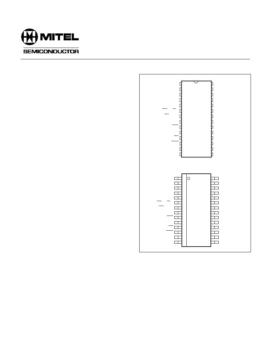
DP28
MP28
Fig. 1 Pin connections ≠ top view (not to scale)
MOTEL is a registered Trademark of Intel Corp. and Motorola Corp.
AD
2
AD
1
AD
0
VDD
ZPPB
ZPPY
ZPPR
WSS
RPHT
SET TRIP
YPHT
BPHT
V
SS
BPHB
AD
3
AD
4
AD
5
AD
6
AD
7
WR* (R/W)
RD* (DS)
ALE* (AS)
RST
CLK
CS
TRIP
RPHB
YPHB
*
= Intel bus format
= Motorola bus format
1
2
3
4
5
6
7
8
9
10
11
12
13
14
28
27
26
25
24
23
22
21
20
19
18
17
16
15
SA828
SA828
1
2
3
4
5
6
7
8
9
10
11
12
13
14
28
27
26
25
24
23
22
21
20
19
18
17
16
15
AD
2
AD
1
AD
0
VDD
ZPPB
ZPPY
ZPPR
WSS
RPHT
SET TRIP
YPHT
BPHT
V
SS
BPHB
AD
3
AD
4
AD
5
AD
6
AD
7
WR* (R/W)
RD* (DS)
ALE* (AS)
RST
CLK
CS
TRIP
RPHB
YPHB
ORDERING INFORMATION
SA8281/IG/DP1S (28-lead DIL, sine + third harmonic
waveform)
SA8282/IG/DP1S (28-lead DIL, sine waveform)
SA8281/IG/MP1S (28-lead SOIC, Sine + third
harmonic waveform)
SA8382/IG/MP1S (28-lead SOIC, sine waveform)
SA828 Family
Three-Phase PWM Waveform Generator
DS4226 - 2.0 November 1996
SA828
2
>4∑5
<0∑2
<10
5∑0
Input high voltage
Input low voltage
Input leakage current
Output high voltage
Output low voltage
Supply current (static)
Supply current (dynamic)
Supply voltage
V
IN
= V
SS
or V
DD
I
OH
= ≠ 12mA
I
OL
= 12mA
All outputs open circuit
f
CLK
= 10MHz
V
IH
V
IL
I
IN
V
OH
V
OL
I
DD (static)
I
DD (dynamic)
V
DD
2
4∑0
4∑5
0∑8
10
0∑4
100
20
5∑5
Typ. Max.
Min.
Value
Characteristic
Symbol
Conditions
Units
ELECTRICAL CHARACTERISTICS
These characteristics are guaranteed over the following conditions (unless otherwise stated):
V
DD
= +5V
±
5%, T
AMB
= +25
∞
C
DC Characteristics
V
V
µ
A
V
V
µ
A
mA
V
-
2/f
CLK
2/f
CLK
Clock frequency
Clock duty cycle
SET TRIP = 1
outputs tripped
TRIP
= 0
M : S ratio = 1 : 1
±
20%
f
CLK
in MHz
f
CLK
in MHz
f
CLK
D
CLK
t
TRIP
12∑5
60
3/f
CLK
3/f
CLK
MHz
%
µ
s
µ
s
NOTE 1. For microprocessor interface timings, see Intel and Motorola bus timings (Tables 1 and 2).
Conditions
Typ. Max.
Characteristic
Symbol
Units
Value
AC Characteristics
ABSOLUTE MAXIMUM RATINGS
Supply voltage, V
DD
Voltage on any pin
Current through any I/O pin
Storage temperature
Operating temperature range
Pin
No.
1
2
3
4
5
6
7
8
9
10
11
12
Name
AD
3
AD
4
AD
5
AD
6
AD
7
Intel:
WR
Motorola:
R/W
Intel:
RD
Motorola: DS
Intel: ALE
Motorola: AS
RST
CLK
CS
TRIP
Type
I
I
I
I
I
I
I
I
I
I
I
O
Function
Multiplexed Address/Data
Multiplexed Address/Data
Multiplexed Address/Data
Multiplexed Address/Data
Multiplexed Address/Data(MSB)
Intel bus control: Write Strobe
Motorola bus control: Read/Write
select
Intel bus control: Read Strobe
Motorola bus control: Data Strobe
Intel bus control: Address Latch
Enable
Motorola bus control: Address
Strobe
Reset internal counters, active low
Clock input
Chip Select input, active low
Output trip status; low = output tripped
Name
RPHB
YPHB
BPHB
V
SS
BPHT
YPHT
SET TRIP
RPHT
WSS
ZPPR
ZPPY
ZPPB
V
DD
AD
0
AD
1
AD
2
Pin
No.
13
14
15
16
17
18
19
20
21
22
23
24
25
26
27
28
Type
O
O
O
P
O
O
I
O
O
O
O
O
P
I
I
I
Function
Red Phase, Bottom power switch
Yellow Phase, Bottom power switch
Blue Phase, Bottom power switch
Negative power supply (0V)
Blue Phase, Top power switch
Yellow Phase, Top power switch
Set output trip. 120k
internal
pull-up resistor
Red Phase, Top power switch
Waveform Sampling Synchronisation
Zero Phase Pulse, Red phase
Zero Phase Pulse, Yellow phase
Zero Phase Pulse, Blue phase
Positive power supply
Multiplexed Address/Data (LSB)
Multiplexed Address/Data
Multiplexed Address/Data
PIN DESCRIPTIONS
The temperature ranges quoted apply to all package types.
Many package types are available and extended temperature
7V
V
SS
≠0∑3V to V
DD
+0∑3V
±
10mA
≠65
∞
C to +125
∞
C
≠40
∞
C to +85
∞
C
40
ranges can be offered for some. Further information is available
on request.
Stresses above those listed in the Absolute Maximum
Ratings may cause permanent damage to the device. These
are stress ratings only and functional operation of the device at
these conditions, or at any other condition above those indicated
in the operations section of this specification, is not implied.
Exposure to Absolute Maximum Rating conditions for extended
periods may affect device reliability.
3
SA828
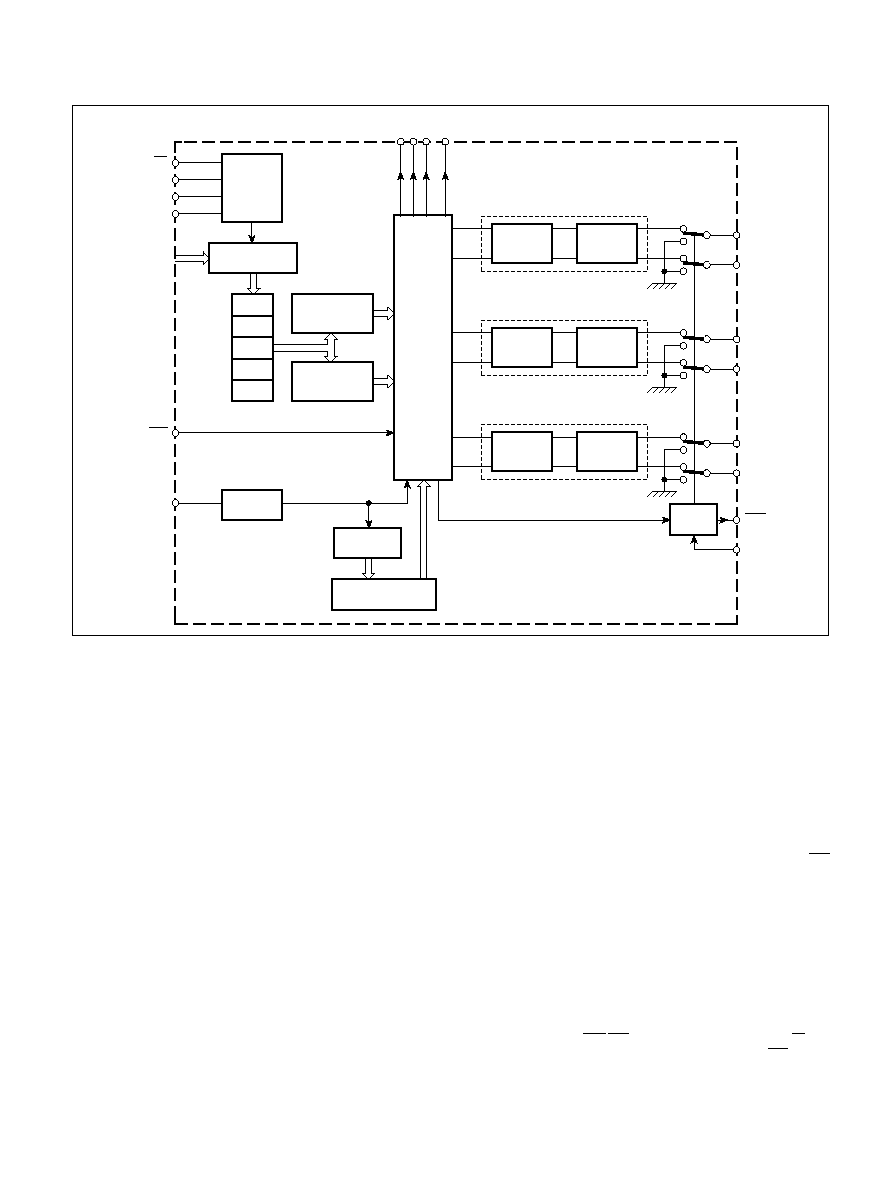
Fig. 2 SA828 internal block diagram
PULSE
DELETION
PULSE
DELAY
CIRCUIT
RPHT
RPHB
PULSE
DELETION
PULSE
DELAY
CIRCUIT
YPHT
YPHB
PULSE
DELETION
PULSE
DELAY
CIRCUIT
BPHT
BPHB
RED PHASE
YELLOW PHASE
BLUE PHASE
PHASING
AND
CONTROL
LOGIC
WAVEFORM
ROM
TRIP
LATCH
ADDRESS
GENERATOR
24-BIT
INITIALISATION
REGISTER
24-BIT
CONTROL
REGISTER
R0
R1
R2
R3
R4
BUS
DEMULTIPLEXER
BUS
CONTROL
CLOCK
DIVIDER
RST
MOTEL
INTERFACE
SYSTEM
BUS
AD
0
-AD
7
8
SET
TRIP
TRIP
CS
CLOCK
ZPP
O/Ps WSS
FUNCTIONAL DESCRIPTION
An asynchronous method of PWM generation is used with
uniform or `double-edged' regular sampling of the waveform
stored in the internal ROM as illustrated in Fig. 3.
The triangle carrier wave frequency is selectable up to 24kHz
(assuming the maximum clock frequency of 12.5MHz is used),
enabling ultrasonic operation for noise critical applications. With
12.5MHz clock, power frequency ranges of up to 4kHz are
possible, with the actual output frequency resolved to 12-bit
accuracy within the chosen range in order to give precise motor
speed control and smooth frequency changing. The output phase
sequence of the PWM outputs can also be changed to allow both
forward and reverse motor operation.
PWM output pulses can be `tailored' to the inverter
characteristics by defining the minimum allowable pulse width
(the SA828 will delete all shorter pulses from the `pure' PWM pulse
train) and the pulse delay (underlap) time, without the need for
external circuitry. This gives cost advantages in both component
savings and in allowing the same PWM circuitry to be used for
control of a number of different motor drive circuits simply by
changing the microprocessor software.
Power frequency amplitude control is also provided with an
overmodulation option to assist in rapid motor braking. Alternatively,
braking may be implemented by setting the rotational speed to
0Hz. This is termed `DC injection braking', in which the rotation of
the motor is opposed by allowing DC to flow in the windings.
A trip input allows the PWM outputs to be shut down immediately,
overriding the microprocessor control in the event of an emergency.
The Waveform Sampling Synchronisation (WSS) output may
be used in conjunction with the ZPP signals to provide feedback
of the actual rotational speed from the rotor. This is of particular
use in slip compensated systems.
Other possible SA828 applications are as a 3-phase waveform
generator as part of a switched-mode power supply (SMPS) or of
an uninterruptible power supply (UPS). In such applications the
high carrier frequency allows a very small switching transformer
to be used.
MICROPROCESSOR INTERFACE
The SA828 interfaces to the controlling microprocessor by
means of a multiplexed bus of the MOTEL format. This interface
bus has the ability to adapt itself automatically to the format and
timing of both MOTorola and IntEL interface buses (hence MOTEL).
Internally, the detection circuitry latches the status of the DS/
RD
line when AS/ALE goes high. If the result is high then the Intel
mode is used; if the result is low then the Motorola mode is used.
This procedure is carried out each time that AS/ALE goes high. In
practice this mode selection is transparent to the user. For bus
connection and timing information refer to the description relevant
to the microprocessor/controller being used.
Industry standard microprocessors such as the 8085, 8088,
etc. and microcontrollers such as the 8051, 8052 and 6805 are all
compatible with the interface on the SA828. This interface consists
of 8 data lines, AD
0
- AD
7
(write-only in this instance), which are
multiplexed to carry both the address and data information, 3 bus
control lines, labelled
WR,RD
and ALE in Intel mode and R/
W
, DS
and AS in Motorola mode, and a Chip Select input,
CS
, which
allows the SA828 to share the same bus as other microprocessor
peripherals. It should be noted that all bus timings are derived from
the microprocessor and are independent of the SA828 clock
input.

SA828
4
Fig. 3 Asynchronous PWM generation with`double-edged' regular sampling as used by the SA828
t
1
ALE
t
4
t
3
t
2
t
8
t
10
t
11
t
9
t
12
RD
WR
AD
0
-AD
7
CS
LATCH ADDRESS
LATCH DATA
t
15
t
4
t
3
t
8
t
10
t
11
t
9
t
12
DS
R/W
AD
0
-AD
7
CS
LATCH ADDRESS
LATCH DATA
t
1
AS
t
2
t
5
t
6
t
7
t
15
+1
≠ 1
+1
≠ 1
RESULTING
PWM
WAVEFORM
0
0
PWM SWITCHING
INSTANTS
TRIANGLE WAVE AT
CARRIER FREQUENCY,
SAMPLING ON +VE AND ≠ VE PEAKS
POWER WAVEFORM
AS READ FROM
INTERNAL ROM
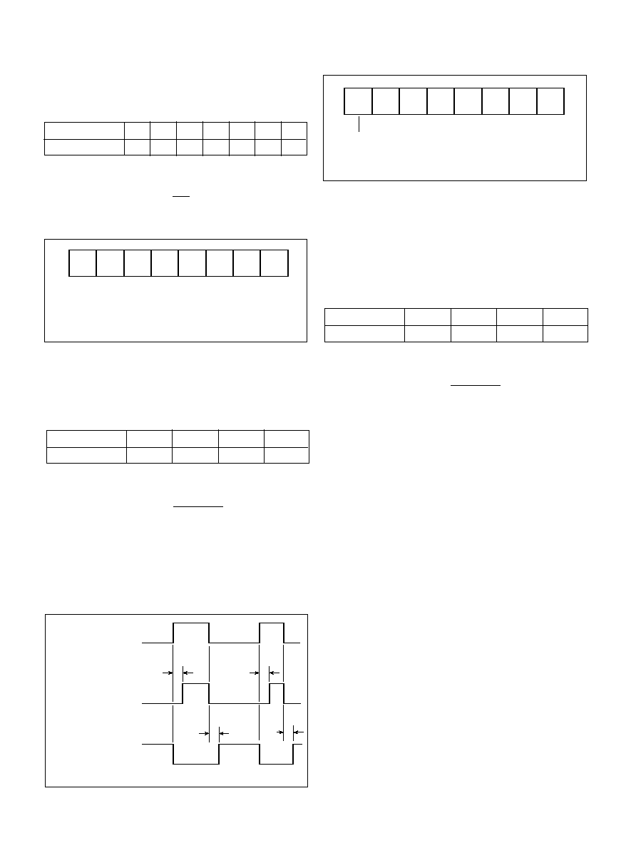
Fig. 5 Motorola bus timing definitions
Parameter
AS high period
Delay time, as low to DS high
DS high period
Delay time, DS low to AS high
DS low period
DS high to R/
W
low setup time
R/
W
hold time
CS
setup time
CS
hold time
Address setup time
Address hold time
Write data setup time
Write data hold time
Symbol
t
1
t
2
t
3
t
4
t
5
t
6
t
7
t
8
t
9
t
10
t
15
t
11
t
12
Min.
90
40
210
40
200
10
10
20
0
30
30
110
30
Table 2 Motorola bus timings at V
DD
= 5V, T
AMB
= +25
∞
C
Units
ns
ns
ns
ns
ns
ns
ns
ns
ns
ns
ns
ns
ns
Fig. 4 Intel bus timing definitions
Parameter
ALE high period
Delay time, ALE to
WR
WR
low period
Delay time,
WR
high to ALE high
CS
setup time
CS
hold time
Address setup time
Address hold time
Data setup time
Data hold time
Symbol
t
1
t
2
t
3
t
4
t
8
t
9
t
10
t
15
t
11
t
12
Min.
70
40
200
40
20
0
30
30
100
25
Table 1 Intel bus timings at V
DD
= 5V, T
AMB
=
+
25
∞
C
Units
ns
ns
ns
ns
ns
ns
ns
ns
ns
ns
5
SA828
Register
R0
R1
R2
R3
R4
Comment
Temporary register R0
Temporary register R1
Temporary register R2
Transfers control data
Transfers initialisation data
AD
1
0
0
1
1
0
Power frequency range
This sets the maximum power frequency that can be carried
within the PWM output waveforms. This would normally be set
to a value to prevent the motor system being operated outside
its design parameters.
Pulse delay time ('underlap')
For each phase of the PWM cycle there are two control
signals, one for the top switch connected to the positive
inverter DC supply and one for the bottom switch connected to
the negative inverter DC supply. In theory, the states of these
two switches are always complementary. However, due to the
finite and non-equal turn-on and turn- off times of power
devices, it is desirable when changing the state of the output
pair, to provide a short delay time during which both outputs
are off in order to avoid a short circuit through the switching
elements.
Pulse deletion time
A pure PWM sequence produces pulses which can vary in
width between 0% and 100% of the duty cycle. Therefore, in
theory, pulse widths can become infinitesimally narrow. In
practice this causes problems in the power switches due to
storage effects and therefore a minimum pulse width time is
required. All pulses shorter than the minimum specified are
deleted.
Counter reset
This facility allows the internal power frequency counter of
the SA828 to be set to zero, disabling the normal frequency
control and giving a 50% output duty cycle.
Initialisation Register Programming
The initialisation register data is loaded in 8-bit segments into
the three 8-bit temporary registers R0-R2. When all the initialisation
data has been loaded into these registers it is transferred into the
24-bit initialisation register by writing to the dummy register R4.
AD
2
0
0
0
0
1
AD
0
0
1
0
1
0
Table 3 SA828 register addressing
Initialisation Register Function
The 24-bit initialisation register contains parameters which,
under normal operation, will be defined during the power-up
sequence. These parameters are particular to the drive circuitry
used, and therefore changing these parameters during a PWM
cycle is not recommended. Information in this register should
only be modified while
RST
is active (i.e. low) so that the PWM
outputs are inhibited (low) during the updating process.
The parameters set in the initialisation register are as follows:
Carrier frequency
Low carrier frequencies reduce switching losses whereas
high carrier frequencies increase waveform resolution and can
allow ultrasonic operation.
Carrier frequency selection
The carrier frequency is a function of the externally applied
clock frequency and a division ratio
n, determined by the 3-bit
CFS word set during initialisation. The values of
n are selected
as shown in Table 4.
The carrier frequency,
f
CARR
, is then given by:
CFS word
Value of n
000
1
001
2
010
4
011
8
100
16
101
32
Table 4 Values of clock division ratio n
FRS
2
FRS
1
FRS
0
X
X
CFS
2
CFS
2
CFS
2
FREQUENCY
RANGE
SELECT WORD
FRS
2
= MSB
FRS
0
= LSB
DON'T
CARE
CARRIER
FREQUENCY
SELECT WORD
CFS
2
= MSB
CFS
0
= LSB
Fig. 6 Temporary register R1
where
k = clock frequency and n = 1, 2, 4, 8, 16 or 32 (as set
by CFS)
Power frequency range selection
The power frequency range selected here defines the maximum
limit of the power frequency. The operating power frequency is
controlled by the 12-bit Power Frequency Select (PFS) word in
the control register but may not exceed the value set here.
k
512 x
n
f
CARR
=
MICROPROCESSOR BUS TIMING
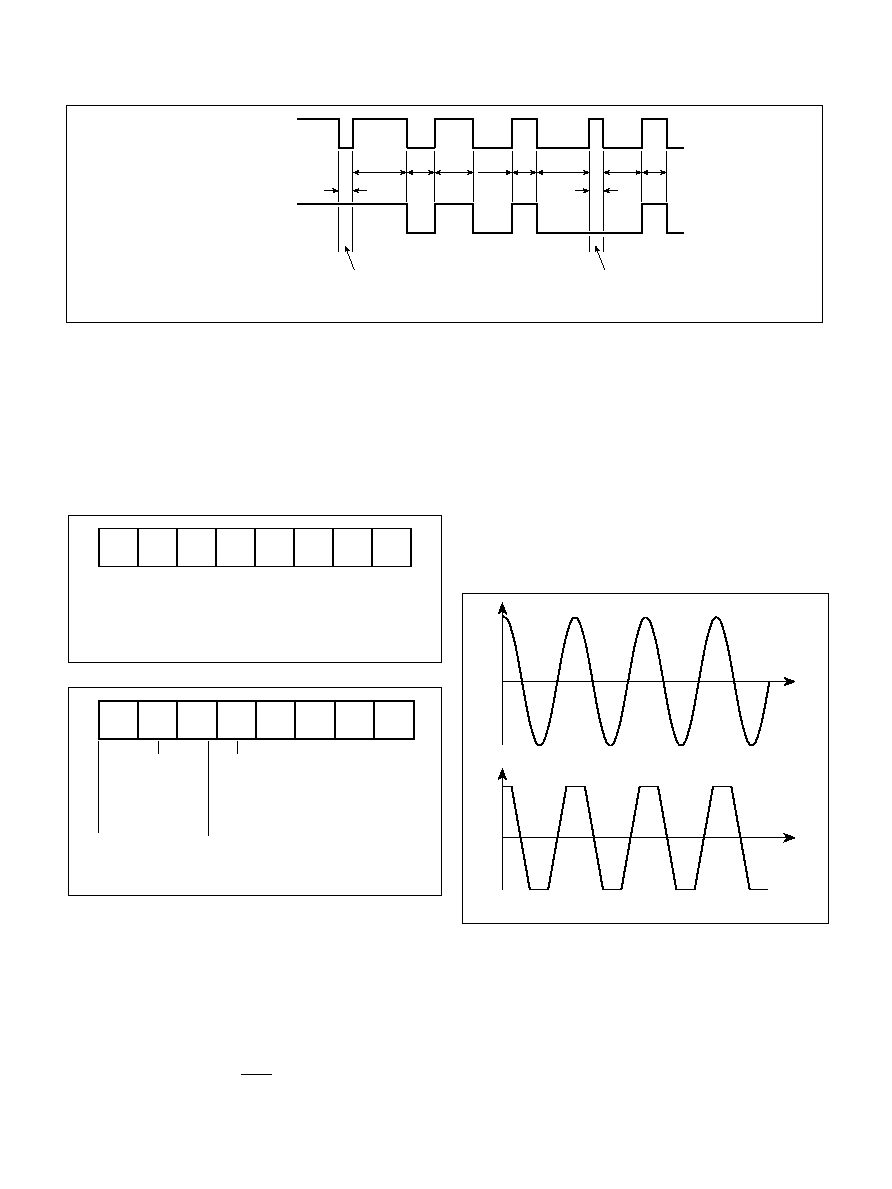
Intel Mode (Fig. 4 and Table 1)
The address is latched by the falling edge of ALE. Data is
written from the bus into the SA828 on the rising edge of
WR.
RD
is not used in this mode because the registers in the SA828
are write only. However, this pin must be connected to
RD
(or
tied high) to enable the SA828 to select the correct interface
format.
Motorola Mode (Fig. 5 and Table 2)
The address is latched on the falling edge of the AS line. Data
is written from the bus into the SA828 (only when R/
W
is low) on
the falling edge of DS (providing
CS i
s low).
CONTROLLING THE SA828
The SA828 is controlled by loading data into two 24-bit
registers via the microprocessor interface. These registers are
the initialisation register and the control register.
The initialisation register would normally be loaded before
motor operation (i.e., prior to the PWM outputs being activated)
and sets up the basic operating parameters associated with the
motor and inverter. This data would not normally be updated
during motor operation.
The control register is used to control the PWM outputs (and
hence the motor) during operation e.g., stop/start, speed,
forward/reverse etc. and would normally be loaded and changed
only after the initialisation register has been loaded.
As the MOTEL bus interface is restricted to an 8-bit wide
format, data to be loaded into either of the 24-bit registers is first
written to three 8-bit temporary registers R0, R1 and R2 before
being transferred to the desired 24-bit register. The data is
accepted (and acted upon) only when transferred to one of the
24-bit registers.
Transfer of data from the temporary registers to either the
initialisation register or the control register is achieved by a write
instruction to a dummy register. Writing to dummy register R3
results in data transfer from R0, R1 and R2 to the control
register, while writing to dummy register R4 transfers data from
R0, R1 and R2 to the initialisation register. It does not matter
what data is written to the dummy registers R3 and R4 as they
are not real registers. It is merely the write instruction to either
of these registers which is acted upon in order to load the
initialisation and control registers.
SA828
6
pdy
f
CARR
x 512
Counter reset
When the CR bit is active (i.e., Iow) the internal power
frequency phase counter is set to 0 degrees for the red
phase. It will remain at 0 degrees until the CR bit is released
(i.e., high).
Control Register Function
This 24-bit register contains the parameters that would
normally be modified during PWM cycles in order to control
the operation of the motor.
The parameters set in the control register are as follows:
Power frequency (speed)
Allows the power frequency of the PWM outputs to be
adjusted within the range specified in the initialisation register
Forward/reverse
Allows the direction of rotation of the AC motor to be
changed by changing the phase sequence of the PWM
outputs.
Power frequency amplitude
By altering the widths of the PWM output pulses while
maintaining their relative widths, the amplitude of the power
waveform is effectively altered whilst maintaining the same
power frequency.
Overmodulation
Allows the output waveform amplitude to be doubled so
that a quasi-squarewave is produced. A combination of
overmodulation and a lower power frequency can be used to
achieve rapid braking in AC motors.
Output inhibit
Allows the outputs to be set to the low state while the PWM
generation continues internally. Useful for temporarily
inhibiting the outputs without having to to change other
register contents.
The power frequency range is a function of the carrier
waveform frequency (
f
CARR
) and a multiplication factor
m,
determined by the 3-bit FRS word. The value of
m is determined
as shown in Table 5.
FRS word
Value of m
000
1
001
2
010
4
011
8
100
16
101
32
Table 5 Values of carrier frequency multiplicaion factor m
110
64
The power frequency range,
f
RANGE
, is then given by:
where
f
CARR
= carrier frequency and
m = 1, 2, 4, 8, 16, 32 or 64
(as set by FRS).
f
CARR
384
f
RANGE
=
x
m
X
X
PDY
5
PDY
4
PDY
3
PDY
2
PDY
1
PDY
0
DON'T
CARE
PULSE
DELAY
SELECT WORD
PDY
5
= MSB
PDY
0
= LSB
Fig. 7 Temporary register R2
PDY word
Value of pdy
000000
64
...etc...
...etc...
111110
2
Table 6 Values of pdy
111111
1
The pulse delay time,
t
pdy
, is then given by:
where
pdy = 1- 64 (as set by PDY) and f
CARR
= carrier
frequency.
Fig 8 shows the eftect of the pulse delay circuit.
It should be noted that as the pulse delay circuit follows the
pulse deletion circuit (see Fig. 2), the minimum pulse width
seen at the PWM outputs will be shorter than the pulse deletion
time set in the initialisation register. The actual shortest pulse
generated is given by
t
pd
≠
t
pdy
.
Pulse delay time
The pulse delay time affects all six PWM outputs by delaying
the rising edges of each of the outputs by an equal amount.
The pulse delay time is a function of the carrier waveform
frequency and
pdy, defined by the 6-bit pulse delay time select
word (PDY). The value of
pdy is selected as shown in Table 6.
Fig. 8 Effect of pulse delay on PWM pulse train
PWM SIGNAL
REQUIRED AT
INVERTER OUTPUT
t
pdy
t
pdy
t
pdy
t
pdy
OUTPUT SIGNAL TO
DRIVE TOP SWITCH
INVERTER ARM
OUTPUT SIGNAL TO
DRIVE BOTTOM SWITCH
INVERTER ARM
t
pdy
= PULSE DELAY TIME
t
pdy
=
CR
PDT
6
PDT
5
PDT
4
PDT
3
PDT
2
PDT
1
PDT
0
COUNTER
RESET
PULSE DELETION
TIME
SELECT WORD
PDT
6
= MSB
PDT
0
= LSB
Fig. 9 Temporary register R0
Pulse deletion time
To eliminate short pulses the true PWM pulse train is passed
through a pulse deletion circuit. The pulse deletion circuit
compares pulse widths with the pulse deletion time set in the
initialisation register. lf a pulse (either positive or negative) is
greater than or equal in duration to the pulse deletion time, it is
passed through unaltered, otherwise the pulse is deleted.
The pulse deletion time,
t
pd
, is a function of the carrier wave
frequency and
pdt, defined by the 7-bit pulse deletion time word
(PDT). The value of
pdt is selected as shown in Table 7.
PDT word
Value of pdt
0000000
128
...etc...
...etc...
1111110
2
Table 7 Values of pdt
1111111
1
The pulse deletion time,
t
pd
, is then given by:
where
pdt = 1-128 (as set by PDT) and f
CARR
= carrier frequency.
Fig. 10 shows the effect of pulse deletion on a pure PWM
waveform.
t
pd
=
pdt
f
CARR
x 512
7
SA828
Fig. 10 The effect of the pulse deletion circuit
PWM SIGNAL
BEFORE
PULSE DELETION
<t
pd
>t
pd
t
pd
= PULSE DELETION TIME
<t
pd
>t
pd
>t
pd
>t
pd
>t
pd
>t
pd
>t
pd
>t
pd
PWM SIGNAL
AFTER
PULSE DELETION
PULSE
DELETED
PULSE
DELETED
where
pfs = decimal value of the 12-bit PFS word and f
RANGE
=
power frequency range set in the initialisation register.
PFS
7
PFS
6
PFS
5
PFS
4
PFS
3
PFS
2
PFS
1
PFS
0
POWER
FREQUENCY
SELECT WORD
BITS 0-7
PFS0
= LSB
Fig. 11 Temporary register R0
F/R
OM
INH
X
PFS
11
PFS
10
PFS
9
PFS
8
POWER
FREQUENCY
SELECT WORD
BITS 8-11
PFS11
= MSB
DON'T
CARE
OVERMOD-
ULATION
BIT
0 = DISABLED
1 = ACTIVE
OUTPUT
INHIBIT BIT
0 = OUTPUTS DISABLED
1 = OUTPUTS ACTIVE
FORWARD/
REVERSE BIT
0 = FORWARD
1 = REVERSE
Fig. 12 Temporary register R1
Power frequency selection
The power frequency is selected as a proportion of the power
frequency range (defined in the initialisation register) by the 12-
bit power frequency select word, PFS, allowing the power
frequency to be defined in 4096 equal steps. As the PFS word
spans the two temporary registers R0 and R1 it is therefore
essential, when changing the power frequency, that both these
registers are updated before writing to R3.
The power frequency (
f
POWER
) is given by:
Control Register Programming
The control register should only be programmed once the
initialisation register contains the basic operating parameters of
the SA828.
As with the initialisation register, control register data is
loaded into the three 8-bit temporary registers R0 - R2. When all
the data has been loaded into these registers it is transferred
into the 24-bit control register by writing to the dummy register
R3. It is recommended that all three temporary registers are
updated before writing to R3 in order to ensure that a conformal
set of data is transferred to the control register for execution.
f
RANGE
4096
f
POWER
=
x pfs
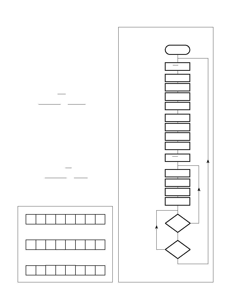
OVERMODULATION BIT NOT SET
(100% MODULATION)
OVERMODULATION BIT SET
(200% MODULATION)
V
V
0
0
t
t
Fig. 13 Current waveforms as seen at the motor terminals,
showing the effect of setting the overmodulation bit
Forward/ reverse selection
The phase sequence of the three-phase PWM output
waveforms is controlled by the Forward/Reverse bit F/R. The
actual effect of changing this bit from 0 (forward) to 1 (reverse)
is to reverse the power frequency phase counter from
incrementing the phase angle to decrementing it. The required
output waveforms are all continuous with time during a forward/
reverse change.
In the forward mode the output phase sequence is red-
yellow-blue and in the reverse mode the sequence is blue-
yellow-red.
Output inhibit selection
When active (i.e., Iow) the output inhibit bit INH sets all the
PWM outputs to the off (low) state. No other internal operation
of the device is affected. When the inhibit is released the PWM
outputs continue immediately. Note that as the inhibit is asserted
after the pulse deletion and pulse delay circuits, pulses shorter
than the normal minimum pulse width may be produced initially.
Overmodulation selection
The overmodulation bit OM is, in effect, the ninth bit (MSB)
of the amplitude word. When active (i.e., high) the output
waveform will be controlled in the 100% to 200% range by the
amplitude word.
The percentage amplitude control is now given by:
Overmodulated Amplitude =
A
POWER
+ 100%
where
A
POWER
= the power amplitude

SA828
8
SA828 PROGRAMMING EXAMPLE
The following example assumes that a master clock of
12∑288 MHz is used (12∑288 MHz crystals are readily available).
This clock frequency will allow a maximum carrier frequency of
24 kHz and a maximum power frequency of 4 kHz.
Initialisation Register Programming Example
A power waveform range of up to 250Hz is required with a
carrier frequency of 6kHz, a pulse deletion time of 10
µ
s and an
underlap of 5
µ
s.
1. Setting the carrier frequency
The carrier frequency should be set first as the power
frequency, pulse deletion time and pulse delay time are all
defined relative to the carrier frequency.
We must calculate the value of
n that will give the required
carrier frequency:
From Table 4,
n = 4 corresponds to a 3-bit CFS word of
010 in temporary register R1.
2. Setting the power frequency range
We must calculate the value of
m that will give the required
power frequency:
From Table 5,
m = 16 corresponds to a 3-bit FRS word of
100 in temporary register R1.
3. Setting the pulse delay time
As the pulse delay time affects the actual minimum pulse width
seen at the PWM outputs, it is sensible to set the pulse delay time
before the pulse deletion time, so that the effect of the pulse delay
time can be allowed for when setting the pulse deletion time.
12∑288 x 10
6
512 x 6 x 10
3
n =
=
= 4
AMP
7
AMP
6
AMP
5
AMP
4
AMP
3
AMP
2
AMP
1
AMP
0
AMPLITUDE
SELECT WORD
AMP
7
= MSB
AMP0
= LSB
Fig.14 Temporary register R2
Amplitude selection
The power waveform amplitude is determined by scaling
the amplitude of the waveform samples stored in the ROM by
the value of the 8-bit amplitude select word (AMP).
The percentage amplitude control is given by:
where
A = decimal value of AMP.
POWER-UP C0NDITIONS
All bits in both the Initialisation and Control registers power-
up in an unidentified state. Holding
RST
low or using the SET
TRIP input will ensure that the PWM outputs remain inactive
(i.e., low) until the device is initialised.
Power Amplitude,
A
POWER
=
x
100%
f
CARR
=
k
512 x
f
CARR
f
RANGE
=
x
m
m =
=
= 16
f
CARR
384
f
RANGE
x 384
f
CARR
250 x 384
6 x 10
3
A
255
k
512 x
n
However, the value of
pdy must be an integer. As the
purpose of the pulse delay is to prevent `shoot-through' (where
both top and bottom arms of the inverter are on simultaneously),
it is sensible to round the pulse delay time up to a higher, rather
than a lower figure.
Thus, if we assign the value 16 to
pdy this gives a delay time
of 5∑2
µ
s. From Table 6,
pdy = 16 corresponds to a 6-bit PDY
word of 110000 in temporary register R2.
4. Setting the pulse deletion time
In setting the pulse deletion time (i.e., the minimum pulse
width) account must be taken of the pulse delay time, as the
actual minimum pulse width seen at the PWM outputs is equal
to
t
pd
≠
t
pdy
.
Therefore, the value of the pulse deletion time must, in this
instance, be set 5∑2
µ
s longer than the minimum pulse length
required
Minimum pulse length required = 10
µ
s
t
PD
to be set to 10
µ
s + 5∑2
µ
s = 15∑2
µ
s
Now,
pdt =
f
pd
x
f
CARR
x 512
= 15∑2 x 10
≠6
x 6 x 10
3
x 512 = 46∑7
t
pd
=
Again,
pdt must be an integer and so must be either rounded
up or down ≠ the choice of which will depend on the application.
Assuming we choose in this case the value 46 for
pdt, this gives
a value of
t
pd
, of 15
µ
s and an actual minimum pulse width of 15
≠ 5∑2
µ
s = 9∑8
µ
s.
From Table 7,
pdt = 46 corresponds to a value of PDT, the
7-bit word in temporary register R0 of 1010010.
The data which must be programmed into the three temporary
registers R0, R1 and R2 (for transfer into the initialisation
register) in order to achieve the parameters in the example
given, is shown in Fig. 15.
Fig. 15
1
1
0
1
0
0
1
0
CR
PDT
6
PDT
5
PDT
4
PDT
3
PDT
2
PDT
1
PDT
0
Temporary Register R0
1
0
0
X
X
0
1
0
Temporary Register R1
FRS
2
FRS
1
FRS
0
X
X
CFS
2
CFS
2
CFS
2
X
X
1
1
0
0
0
0
Temporary Register R2
X
X
PDY
5
PDY
4
PDY
3
PDY
2
PDY
1
PDY
0
We must calculate the value of
pdy that will give the required
pulse delay time:
pdy =
t
pdy
x
f
CARR
x 512
= 5 x 10
≠6
x 6 x 10
3
x 512 = 15∑4
pdy
f
CARR
x 512
t
pdy
=
pdt
f
CARR
x 512
9
SA828
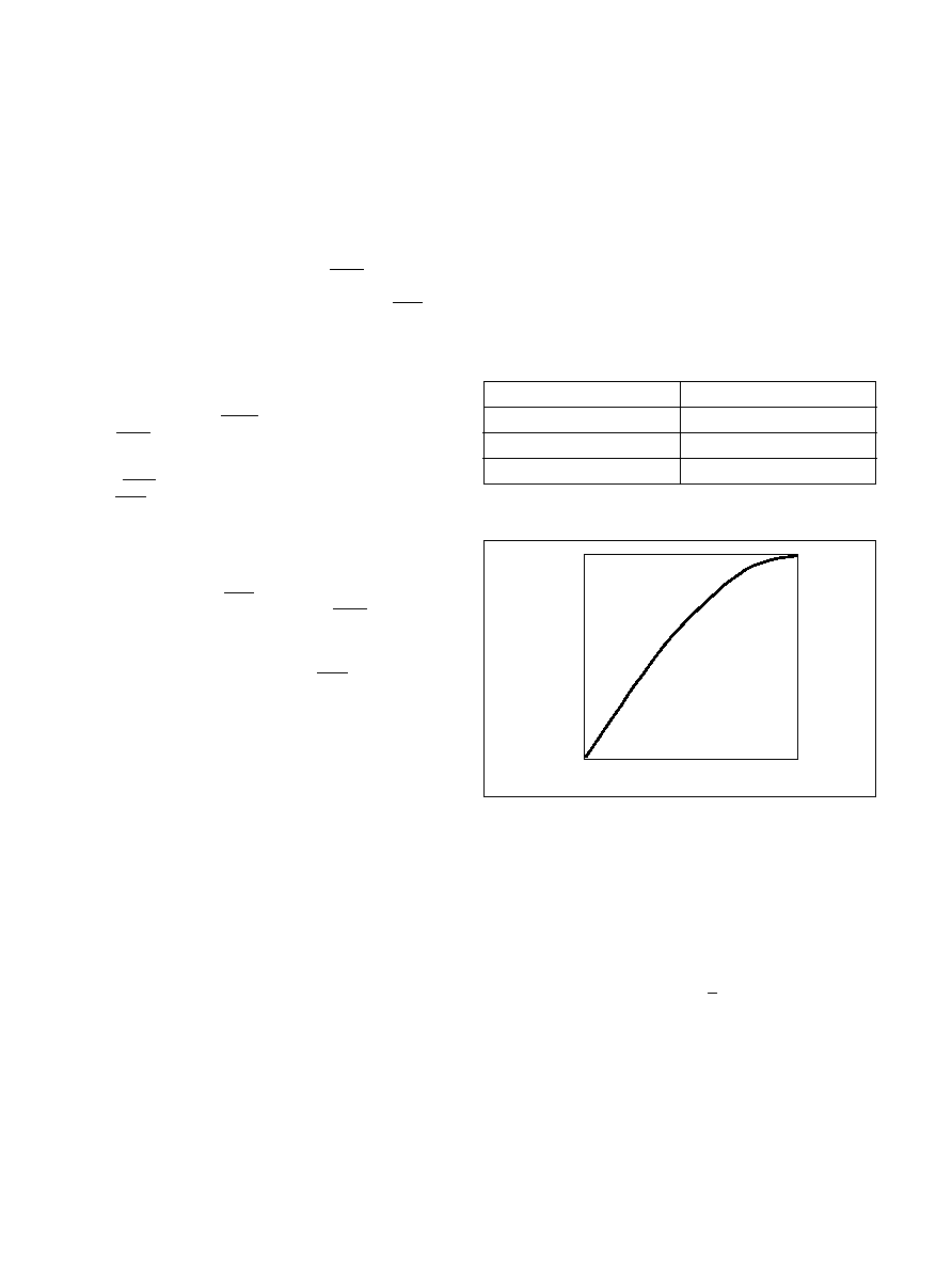
Fig. 17 Typical SA828 programming routine
WRITE R1
WRITE R2
WRITE R4
POWER ON
WRITE R0
RST
0
RST
1
CHANGE
CONTROL
DATA ?
CHANGE
INITIALISATION
DATA ?
YES
NO
YES
NO
WRITE R1
WRITE R2
WRITE R3
WRITE R0
WRITE R1
WRITE R2
WRITE R3
WRITE R0
WRITE
INITIALISATION
DATA
WRITE TO CONTROL
REGISTER INHIBITING
PWM OUTPUTS
BEFORE COMPLETING
RESET CYCLE
ENABLE
PWM OUTPUTS
WRITE
CONTROL
DATA
Control Register Programming Example
The control register would normally be updated many times
while the motor is running, but just one example is given here.
It is assumed that the initialisation register has already heen
programmed with the parameters given in the previous example.
A power waveform of 100Hz is required with a PWM
waveform amplitude of 80% of that stored in the ROM. The
phase sequence should be set to give forward motor rotation.The
outputs should be enabled and no overmodulation is required.
1. Setting the power frequency
The power frequency,
f
POWER
, can be selected to 12-bit
accuracy (i.e 4096 equal steps) from 0Hz to
f
RANGE
as defined
in the initialisation register. In this case, with
f
RANGE
= 250Hz,
the power frequency can be adjusted in increments of 0∑06Hz.
We can only have
pfs as an integer, so if we assign pfs =
1638 this gives
f
POWER
= 99.97 Hz.The 12-bit binary equivalent
of this value gives a PFS word of 011001100110 in temporary
registers R0 and R1.
2. Setting overmodulation, forward/reverse, output inhibit
Overmodulation is not required therefore OM = 0.
Forward motor control is required (i.e., the phase sequence
of the PWM outputs should be red-yellow-blue) therefore forward/
reverse bit F/R = 0.
Output inhibit should be inactive (i e., the outputs should be
active), therefore INH= 1.
These bits are all set in temporary register R1.
3. Setting the power waveform amplitude
A
POWER
x 255
100
A
POWER
=
x
100%
0
1
1
0
0
0
1
1
Temporary Register R0
0
0
1
X
0
1
1
0
Temporary Register R1
1
1
0
0
Temporary Register R2
1
1
0
0
PFS
7
PFS
6
PFS
5
PFS
4
PFS
3
PFS
2
PFS
1
PFS
0
F/R
OM
INH
X
PFS
11
PFS
10
PFS
9
PFS
8
AMP
7
AMP
6
AMP
5
AMP
4
AMP
3
AMP
2
AMP
1
AMP
0
Fig. 16
The 8-bit binary equivalent of this value gives an AMP word
of 11001100 in temporary register R2. The data which must be
programmed into the three temporary registers R0, R1 and R2
(for transfer into the control register) in order to achieve the
parameters in the example given, is shown in Fig. 16.
80 x 255
100
A =
=
= 204
f
POWER
x 4096
f
RANGE
f
RANGE
4096
pfs =
=
= 1638∑4
100 x 4096
250
A
225
f
POWER
=
x pfs
SA828
10
PRODUCT DESIGNATION
Two standard options exist, defining waveform shape. These
are designated SA828-1 and SA828-2 as follows:
SA828-1
Sine + third harmonic at one-sixth the amplitude of the
fundamental:
x(t) = A [sin (
t) + sin 3(
t)]
SA828-2
Pure sinewave:
x(t) = A [sin (
t)]
Additional wave shapes can be implemented to order, provided
they are symmetrical about the 90
∞
, 180
∞
and 270
∞
axes.
Contact your local Mitel Semiconductor Customer Service
Centre for further details.
1
6
HARDWARE INPUT/OUTPUT FUNCTIONS
Set Output Trip (SET TRIP input)
The SET TRIP input is provided separately from the
microprocessor interface in order to allow an external source
to override the microprocessor and provide a rapid shutdown
facility. For example, logic signals from overcurrent sensing
circuitry or the microprocessor `watchdog' might be used to
activate this input.
When the SET TRIP input is taken to a logic high, the output
trip latch is activated. This results in the
TRIP
output and the
six PWM outputs being latched low immediately. This condition
can only be cleared by applying a reset cycle to the
RST
input.
It is essential that when not in use SET TRIP is tied low and
isolated from potential sources of noise; on no account should
it be left floating.
SET TRIP is latched internally at the master clock rate in
order to reduce noise sensitivity.
Output Trip Status (
TRIP
output)
The
TRIP
output indicates the status of the output trip latch
and is active low.
Reset (
RST
input)
The
RST
input performs the following functions when active
(low):
1. All PWM outputs are forced low (if not already low) thereby
turning off the drive switches.
2. All internal counters are reset to zero (this corresponds to 0
∞
for the red phase output).
3. The rising edge of
RST
reactivates the PWM outputs
resetting the output trip and setting the
TRIP
output high ≠
assuming that the SET TRIP input is inactive (i.e. Iow).
A sixth register, R5, located at A2:O = 101 is used to place
the device into a factory test mode. This is achieved by writing
dummy data to R5 immediately after
RST
goes high. Care
must be exercised to ensure that the microprocessor/controller
cannot write to this register.
Zero Phase Pulses (ZPPR, ZPPY and ZPPB outputs)
The zero phase pulse outputs provide pulses at the same
frequency as the power frequency with a 1 : 2 mark-space
ratio. When in the forward mode of operation the falling edge
of ZPPR corresponds to 0
∞
for the red phase, the falling edge
of ZPPY to 0
∞
for the yellow phase and the ZPPB falling edge
to 0
∞
for the blue phase. In the reverse mode, the rising edge
of a zero phase pulse corresponds to 0
∞
for the relevant phase
PWM output.
Waveform Sampling Synchronisation (WSS output)
This output provides a square wave signal of 50% duty
cycle at a frequency 1536 times higher than the fundamental
of the power waveform. Each successive pulse of WSS
corresponds to the SA828 reading the next location of the
waveform ROM. It may be used in conjunction with the ZPP
signals to monitor the position of the machine rotor and may
form part of a closed loop control system such as slip
compensation.
Clock (CLK input)
The CLK input provides a timing reference used by the
SA828 for all timings related to the PWM outputs. The
microprocessor interface, however, derives all its timings from
the microprocessor and therefore the microprocessor and the
SA828 may be run either from the same or from different
clocks.
WAVEFORM DEFINITION
The waveform amplitude data used to construct the PWM
output sequences is read from the internal 384X8 ROM. This
contains the 90
∞
span of the waveform as shown in Fig. 18.
Each successive 8-bit sample linearly represents the
instantaneous amplitude of the waveform. It is assumed that
the waveform is symmetrical about the 90
∞
, 180
∞
and 270
∞
axes.
The SA828 reconstructs the full 360
∞
waveform by reading the
0
∞
-90
∞
section held in ROM and assigning negative values for
the second half of the cycle.
These samples are used to calculate the instantaneous
amplitudes for all three phases, which will be 120
∞
transposed
in the normal R-Y-B orientation for forward rotation or B-Y-R for
reverse rotation. The 384 8-bit samples are regularly spaced
over the 0
∞
to 90
∞
span, giving an angular resolution of
approximately 0∑23
∞
.
Waveform segment
0
∞
- 30
∞
30∑23
∞
- 60
∞
60∑23
∞
- 89∑77
∞
Sample number
0 - 127
128 - 255
256 - 383
Table 8 90
∞
of the 360
∞
cycle is divided into 384 8-bit
samples
Fig. 18 90
∞
sample of typical power waveform
VALUE
OF
8-BIT
SAMPLE
0
∞
45
∞
90
∞
255
0
PHASE (384-BIT RESOLUTION)
POWER
WAVEFORM
11
SA828
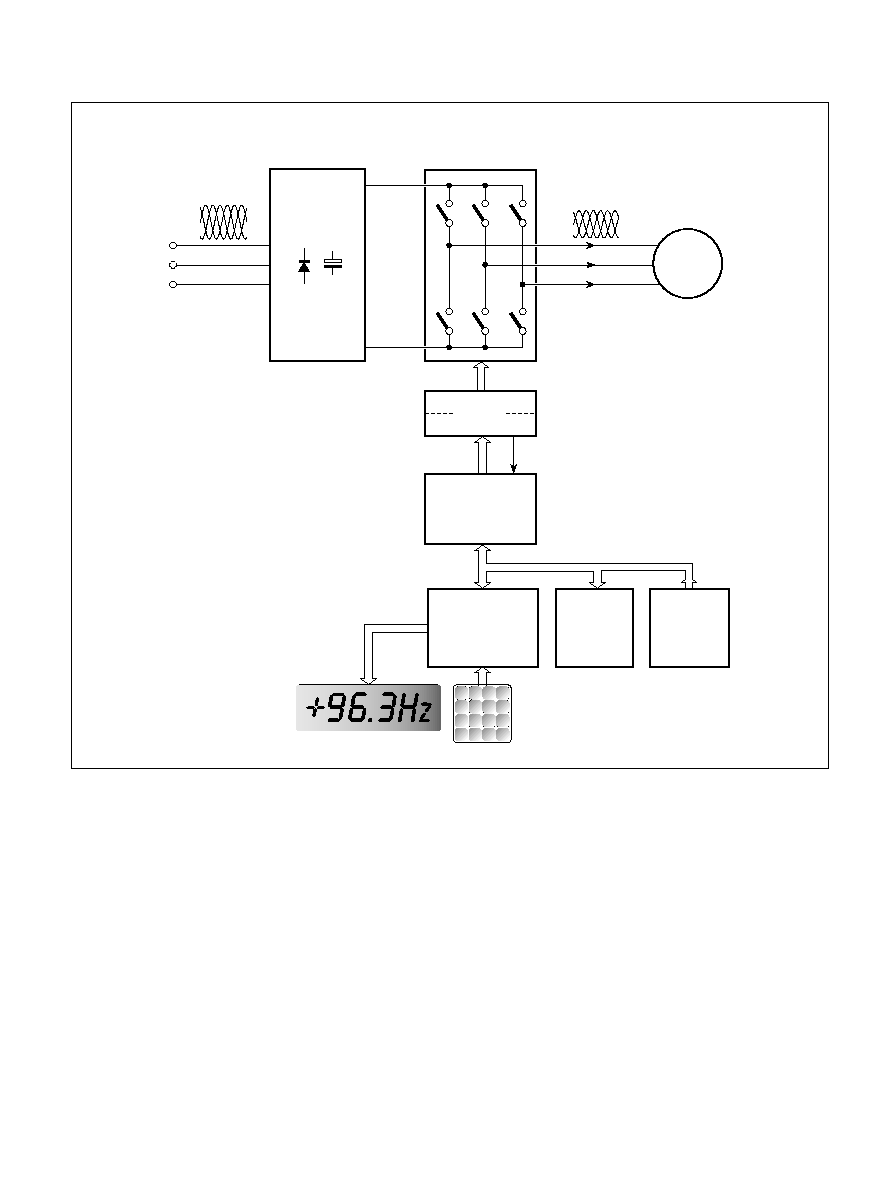
Fig. 19 A typical SA828 application
3-PHASE
VARIABLE VOLTAGE,
VARIABLE FREQUENCY
WAVEFORM
3-PHASE AC
INDUCTION
MOTOR
INVERTER
ISOLATOR
TTL LEVEL
PWM
WAVEFORMS
6
6
FAST
SHUTDOWN
SA828
DC LINK
≠
+
SINGLE OR
3-PHASE
POWER
SUPPLY
R
Y
B
RECTIFIER
AND
SMOOTHING
DATA/ADDRESS BUS
(AD
0
-AD
7
)
8
MICROPROCESSOR
OR
MICROCONTROLLER
WITH ON-CHIP
ROM AND RAM
OPTIONAL
EXTERNAL
ROM
OPTIONAL
EXTERNAL
RAM

SA828
12

13
SA828
PACKAGE DETAILS
Dimensions are shown thus: mm (in). For further package information, please contact your local Customer Service Centre.
2∑36/2∑64
(0∑093/0∑104)
28 LEADS AT
1∑27 (0∑050)
NOM. SPACING
17∑70/18∑10
(0∑697/0∑713)
0∑10/0∑30
(0∑004/0∑012)
0∑41/1∑27
(0∑016/0∑050)
0∑25/0∑71
(0∑010/0∑028)
0∑23/0∑33
(0∑009/0∑013)
28-LEAD MINIATURE PLASTIC DIL - MP28
0∑74 (0∑029)
MAX.
◊
45
∞
0∑36/0∑48
(0∑014/0∑019)
7∑40/7∑60
(0∑291/0∑299)
10∑00/10∑64
(0∑394/0∑419)
1
28
SPOT REF.
CHAMFER
REF.
0-8
∞
NOTES
1. Controlling dimensions are inches.
2. This package outline diagram is for guidance
only. Please contact your Mitel Semiconductor
Customer Service Centre for further information.
0∑51 (0∑02)
MIN
0∑38/0∑61
(0∑015/0∑024)
38∑10 (1∑5)
MAX
28-LEAD PLASTIC DIL ≠ DP28
1
28
3∑05 (0∑120)
MIN
PIN 1 REF
NOTCH
14∑73 (0∑58)
MAX
5∑08/(0∑200)
MAX
0∑23/0∑41
(0∑009/0∑016)
15.24 (0∑6)
NOM CTRS
28 LEADS AT 2∑54 (0∑10)
NOM. SPACING
1∑14/1∑65
(0∑045/0∑065)
NOTES
1. Controlling dimensions are inches.
2. This package outline diagram is for guidance only.
Please contact your Mitel Semiconductor Customer
Service Centre for further information.
SEATING PLANE

SA828
14
Internet: http://www.gpsemi.com
CUSTOMER SERVICE CENTRES
q
FRANCE & BENELUX Les Ulis Cedex Tel: (1) 69 18 90 00 Fax : (1) 64 46 06 07
q
GERMANY Munich Tel: (089) 419508-20 Fax : (089) 419508-55
q
ITALY Milan Tel: (02) 6607151 Fax: (02) 66040993
q
JAPAN Tokyo Tel: (03) 5276-5501 Fax: (03) 5276-5510
q
KOREA Seoul Tel: (2) 5668141 Fax: (2) 5697933
q
NORTH AMERICA Scotts Valley, USA Tel: (408) 438 2900 Fax: (408) 438 5576/6231
q
SOUTH EAST ASIA Singapore Tel:(65) 3827708 Fax: (65) 3828872
q
SWEDEN Stockholm Tel: 46 8 702 97 70 Fax: 46 8 640 47 36
q
TAIWAN, ROC Taipei Tel: 886 2 25461260 Fax: 886 2 27190260
q
UK, EIRE, DENMARK, FINLAND & NORWAY
Swindon Tel: (01793) 726666 Fax : (01793) 518582
These are supported by Agents and Distributors in major countries world-wide.
© Mitel Corporation 1998 Publication No. DS4226 Issue No. 2.0 November 1996
TECHNICAL DOCUMENTATION ≠ NOT FOR RESALE. PRINTED IN UNITED KINGDOM
HEADQUARTERS OPERATIONS
MITEL SEMICONDUCTOR
Cheney Manor, Swindon,
Wiltshire SN2 2QW, United Kingdom.
Tel: (01793) 518000
Fax: (01793) 518411
MITEL SEMICONDUCTOR
1500 Green Hills Road,
Scotts Valley, California 95066-4922
United States of America.
Tel (408) 438 2900
Fax: (408) 438 5576/6231
This publication is issued to provide information only which (unless agreed by the Company in writing) may not be used, applied or reproduced for any purpose nor form part of any order or contract nor to be regarded
as a representation relating to the products or services concerned. No warranty or guarantee express or implied is made regarding the capability, performance or suitability of any product or service. The Company
reserves the right to alter without prior notice the specification, design or price of any product or service. Information concerning possible methods of use is provided as a guide only and does not constitute any
guarantee that such methods of use will be satisfactory in a specific piece of equipment. It is the user's responsibility to fully determine the performance and suitability of any equipment using such information and
to ensure that any publication or data used is up to date and has not been superseded. These products are not suitable for use in any medical products whose failure to perform may result in significant injury
or death to the user. All products and materials are sold and services provided subject to the Company's conditions of sale, which are available on request.
All brand names and product names used in this publication are trademarks, registered trademarks or trade names of their respective owners.