 | –≠–ª–µ–∫—Ç—Ä–æ–Ω–Ω—ã–π –∫–æ–º–ø–æ–Ω–µ–Ω—Ç: SP5655KG | –°–∫–∞—á–∞—Ç—å:  PDF PDF  ZIP ZIP |
The SP5655 is a single chip frequency synthesiser designed
for TV tuning systems. Control data is entered in the standard
I
2
C BUS format. The device contains 2 addressable current
limited outputs and 4 addressable bidirectional open-collector
ports, one of which is a 3-bit ADC. The information on these
ports can be read via the I
2
C BUS. the device has one fixed
I
2
C BUS address and 3 programmable addresses,
programmed by applying a specific input voltage to one of the
current limited outputs. This enables two or more synthesisers
to be used in a system.
FEATURES
s
Complete 2∑7GHz Single Chip System
s
High Sensitivity RF Inputs
s
Programmable via I
2
C BUS
s
Low Power Consumption (5V, 30mA)
s
Low Radiation
s
Phase Lock Detector
s
Varactor Drive Amp Disable
s
6 Controllable Outputs, 4 Bidirectional
s
5-Level ADC
s
Variable I
2
C BUS Address for Multi-tuner Applications
s
ESD Protection: 4kV, Mil-Std-883C, Method 3015
(1)
s
Switchable 4512/1024 Reference Divider
s
Pin and Function Compatible with SP5055S
(2)
(1)
Normal ESD handling precautions should be observed.
(2) The SP5055S does not have a switchable reference
division ratio.
SP5655
2∑7GHz Bidirectional I
2
C Bus Controlled Synthesiser
Advance Information
Supersedes July 1996 version, DS3743-4.3
DS3743 - 5.0 June 1998
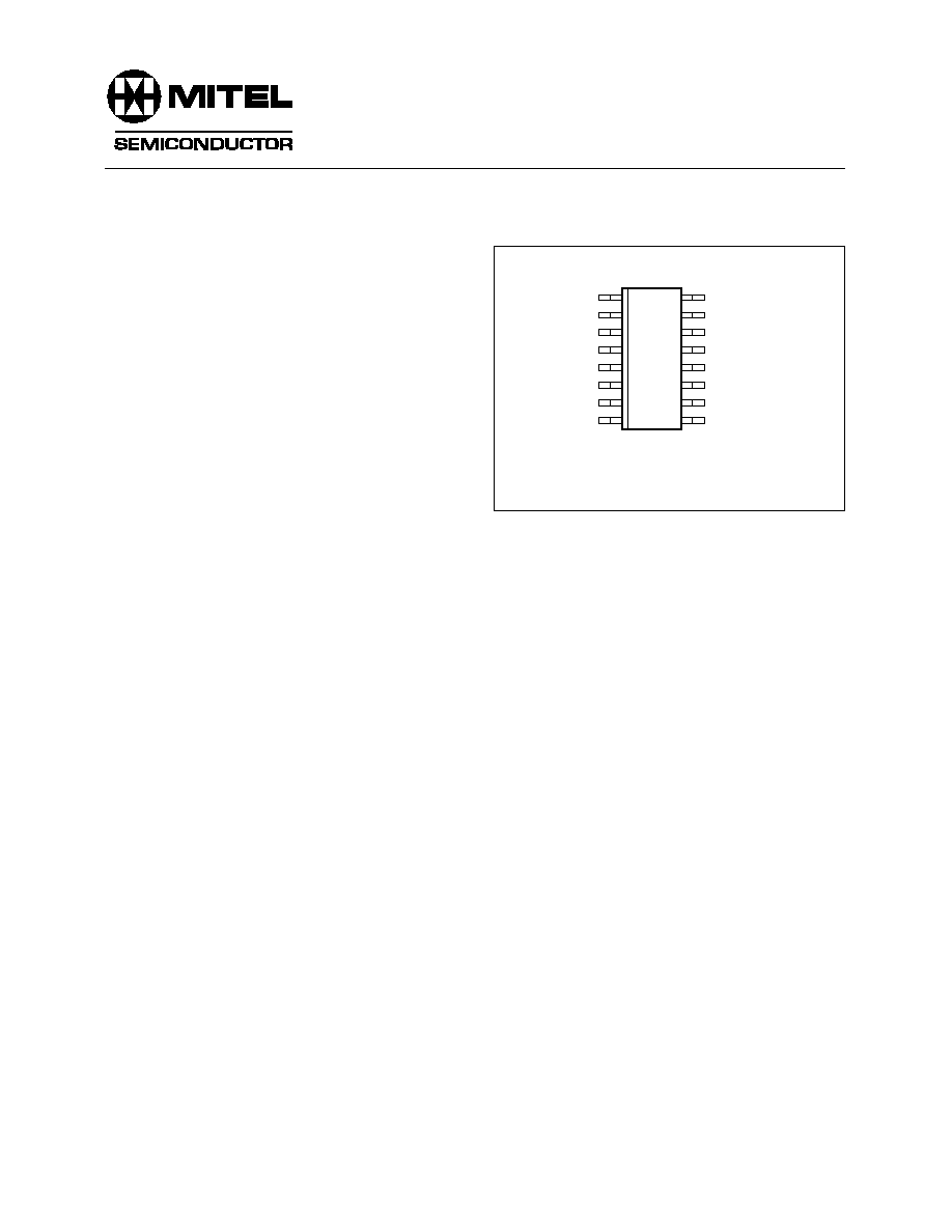
Fig. 1 Pin connections ≠ top view
SP5655
1
2
3
4
5
6
7
8
MP16
16
15
14
13
12
11
10
9
CHARGE PUMP
CRYSTAL Q1
CRYSTAL Q2
SDA
SCL
I/O PORT P7
*
I/O PORT P6
I/O PORT P5
DRIVE OUTPUT
V
EE
RF INPUT
RF INPUT
V
CC
P0 OUTPUT PORT
I/O PORT P4
= Logic level I/O port
*
= 3-bit ADC input
P3 OUTPUT PORT/
ADD SELECT
APPLICATIONS
s
Satellite TV
s
High IF Cable Tuning Systems
THERMAL DATA
u
JC
= 41
∞
C/W
u
JA
= 111
∞
C/W
ORDERING INFORMATION
SP5655 KG/MPAS (Tubes)
SP5655S KG/MPAD (Tape and reel)
2
SP5655
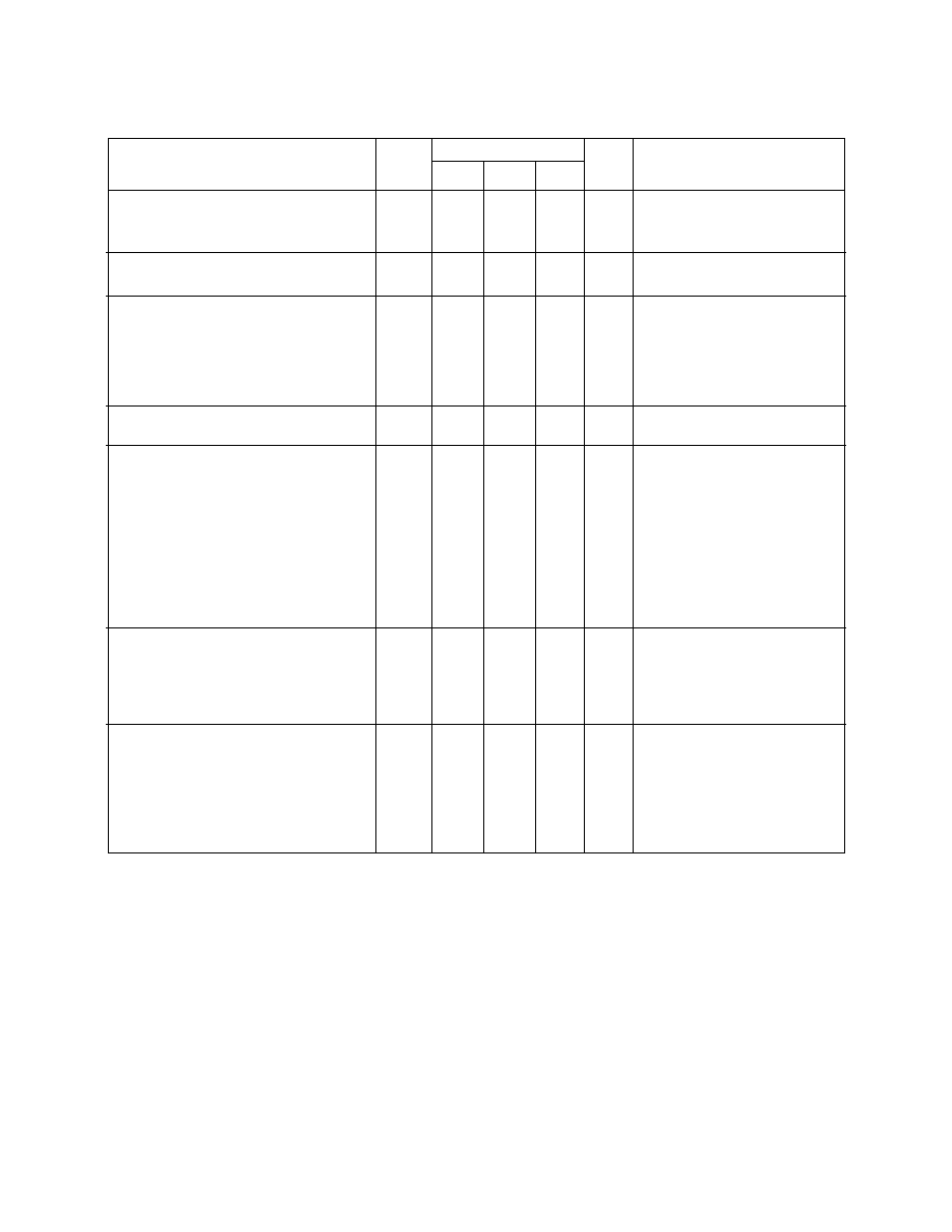
ELECTRICAL CHARACTERISTICS
T
AMB
= 220
∞
C to 180
∞
C, V
CC
= 14∑5V to 15∑5V, reference frequency = 4MHz.
These Characteristics are guaranteed by either production test or design. They apply within the specified ambient temperature
and supply voltage ranges unless otherwise stated.
Supply current
Prescaler input voltage
Prescaler input impedance
Prescaler input capacitance
SDA, SCL
Input high voltage
Input low voltage
Input high current
Input low current
Leakage current
SDA
Output voltage
Charge pump current low
Charge pump current high
Charge pump output leakage current
Charge pump drive output current
Charge pump amplifier gain
Recommended crystal series resistance
Crystal oscillator drive level
Crystal oscillator negative resistance
External reference input frequency
External reference input amplitude
Output Ports
P0, P3 sink current
P0, P3 leakage current
P4-P7 sink current
P4-P7 leakage current
Input Ports
P3 input current high
P3 input current low
P4, P5, P7 input voltage low
P4, P5, P7 input voltage high
P6 input current high
P6 input current low
Typ.
Value
Conditions
Characteristic
Pin
12
13,14
13,14
13, 14
4,5
4,5
4,5
4,5
4,5
4
1
1
1
16
2
2
2
2
11, 10
11, 10
9-6
9-6
10
10
9,8,6
9,8,6
7
7
50
3
0
500
10
750
2
70
0∑7
10
2∑7
30
50
2
6
50
6
170
6400
80
1000
1
40
300
5∑5
1∑5
10
2
10
10
0∑4
6
5
200
8
200
1∑5
10
10
1
10
2
10
0∑8
1
10
2
10
Units
Min.
Max.
mA
mVrms
pF
V
V
µ
A
µ
A
µ
A
V
µ
A
µ
A
nA
µ
A
mV p-p
MHz
mVrms
mA
µ
A
mA
µ
A
µ
A
µ
A
V
V
µ
A
µ
A
V
CC
= 4∑5V to 5∑5V (note 1)
120MHz to 2∑7GHz sinewave,
see Fig. 5
Input voltage = V
CC
Input voltage = 0V
When V
CC
= 0V
Sink current = 3mA
Byte 4, bit 2 = 0, pin 1 = 2V
Byte 4, bit 2 = 1, pin 1 = 2V
Byte 4, bit 4 = 1, pin 1 = 2V
V pin 16 = 0∑7V
Parallel resonant crystal (note 2)
AC coupled sinewave
AC coupled sinewave
V
OUT
= 12V
V
OUT
= 13∑2V
V
OUT
= 0∑7V
V
OUT
= 13∑2V
V pin 10 = V
CC
V pin 10 = 0V
See Table 3 for ADC levels
NOTES
1. Maximum power consumption is 220mW with V
CC
= 5∑5V and all ports off.
2. Resistance specified is maximum under all conditions.
3
SP5655
Supply voltage
RF input voltage
Port voltage
Total port output current
Address select voltage
RF input DC offset
Charge pump DC offset
Drive output DC offset
Crystal oscillator DC offset
SDA, SCL input voltage
Storage temperature
Junction temperature
Parameter
Conditions
Port in off state
Port in on state
Port in on state
12
13,14
6-11
6-9
10, 11
6-9
10
13-14
1
16
2
4,5
Pin
ABSOLUTE MAXIMUM RATINGS
All voltages are referred to V
EE
and pin 3 at 0V
Max.
Min.
Units
7
2∑5
14
6
14
50
V
CC
1
0∑3
V
CC
1
0∑3
V
CC
1
0∑3
V
CC
1
0∑3
V
CC
1
0∑3
6
1
150
1
150
Value
2
0∑3
2
0∑3
2
0∑3
2
0∑3
2
0∑3
2
0∑3
2
0∑3
2
0∑3
2
0∑3
2
0∑3
2
55
V
V p-p
V
V
V
mA
V
V
V
V
V
V
∞
C
∞
C
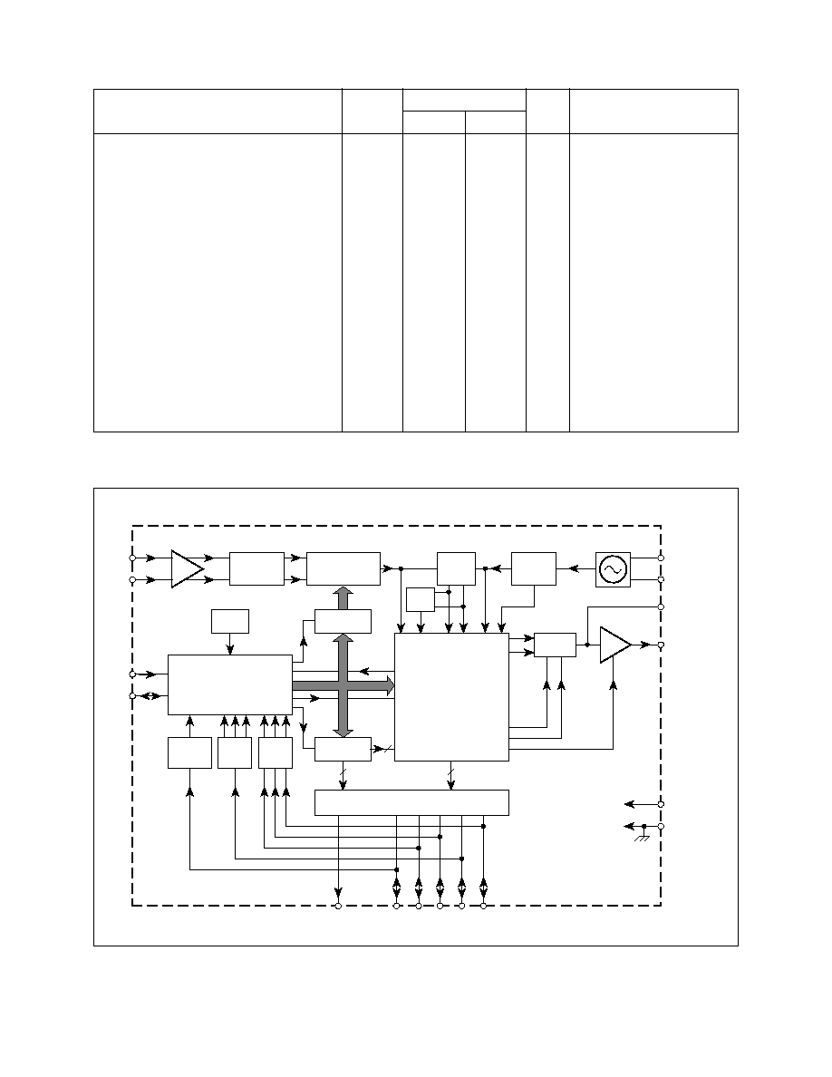
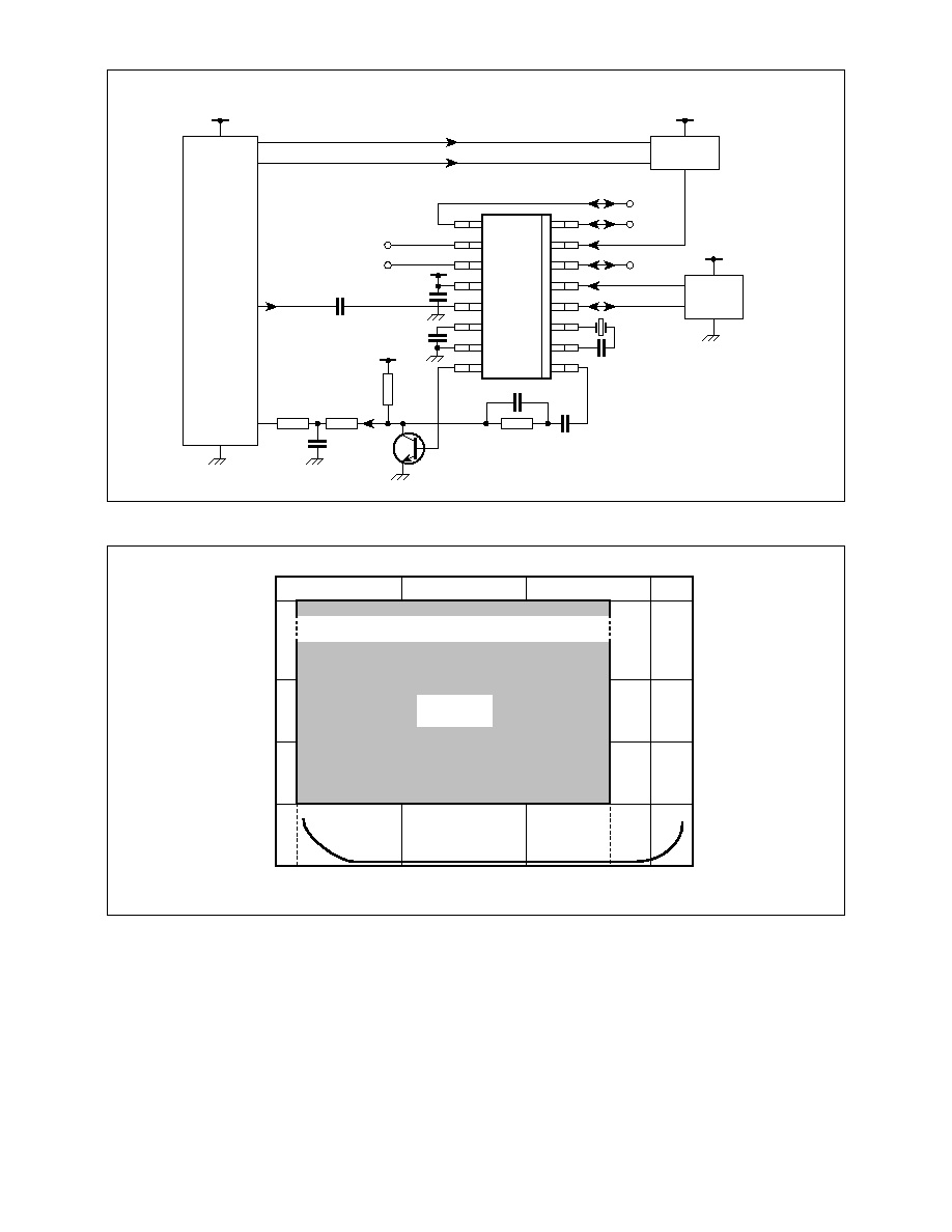
Fig. 2 Block diagram
RF IN
15-BIT
PROGRAMMABLE
DIVIDER
PRESCALER
4
16
POWER
ON DET
I
2
C BUS
TRANSCEIVER
ADDRESS
SELECT
LEVEL
3 TTL
COMP
3-BIT
ADC
POR
PREAMP
SCL
SDA
15-BIT LATCH
DIVIDE RATIO
6-BIT LATCH
PORT INFO
LOCK
DET
PHASE
COMP
F
CONTROL DATA
LATCHES
AND
CONTROL LOGIC
F
L
4
13
14
5
4
CHARGE
PUMP
F
COMP
DIVIDER
4
512/1024
DN
UP
CP
TO
OS
DRIVE/
VARICAP OUT
CHARGE PUMP
Q1
Q2
CRYSTAL
V
CC
V
EE
16
15
1
3
2
OSC
4
PORT OUTPUT DRIVERS
9
8
7
6
P4
P5
P6
P7
F
PD
10
P3
11
P0
2

4
SP5655
FUNCTIONAL DESCRIPTION
The SP5655 is programmed from an I
2
C Bus. Data and
Clock are fed in on the SDA and SCL lines respectively, as
defined by the I
2
C Bus format. The synthesiser can either
accept new data (write mode) or send data (read mode). The
LSB of the address byte (R/W) sets the device into write mode
if it is low and read mode if it is high. The Tables in Fig. 3
illustrate the format of the data. The device can be pro-
grammed to respond to several addresses, which enables the
use of more than one synthesiser in an I
2
C Bus system.
Table 4 shows how the address is selected by applying a
voltage to P3.
When the device receives a correct address byte, it pulls
the SDA line low during the acknowledge period, and during
following acknowledge periods after further data bytes are
programmed. When the device is programmed into the read
mode, the controller accepting the data must pull the SDA line
low during all status byte acknowledge periods to read an-
other status byte. If the controller fails to pull the SDA line low
during this period, the device generates an internal STOP
condition, which inhibits further reading.
WRITE Mode (Frequency Synthesis)
When the device is in write mode bytes 2 and 3 select the
synthesised frequency, while bytes 4 and 5 control the output
port states, charge pump, reference divider ratio and various
test modes.
Once the correct address is received and acknowledged,
the first bit of the next byte determines whether that byte is
interpreted as byte 2 or 4; a logic 0 for frequency information
and a logic 1 for control and output port information. When
byte 2 is received the device always expects byte 3 next.
Similarly, when byte 4 is received the device expects byte 5
next. Additional data bytes can be entered without the need
to readdress the device until an I
2
C stop condition is recog-
nised. This allows a smooth frequency sweep for fine tuning
or AFC purposes.
If the transmission of data is stopped mid-byte (for exam-
ple, by another device on the bus) then the previously pro-
grammed byte is maintained.
Frequency data from bytes 2 and 3 are stored in a 15-bit register
and used to control the division ratio of the 15-bit programmable
divider. This is preceded by a divide-by-16 prescaler and amplifier to
give excellent sensitivity at the local oscillator input, see Fig. 5. The
input impedance is shown in Fig. 7.
The programmed frequency can be calculated by multiply-
ing the programmed division ratio by 16 times the comparison
frequency F
COMP
. When frequency data is entered, the phase
comparator, via a charge pump and varicap drive amplifier,
adjusts the local oscillator control voltage until the output of
the programmable divider is frequency and phased locked to
the comparison frequency.
The reference frequency may be generated by an external
source capacitively coupled into pin 2, or provided by an on-
chip crystal controlled oscillator. The comparison frequency
F
COMP
is derived from the reference frequency via the refer-
ence divider. The reference divider division ratio is switchable
from 512 to 1024, and is controlled by bit 7 of byte 4 (TS0); a
logic 1 to 512, a logic 0 for 1024. The SP5655 differs from the
SP5055 in this respect, only 512 being available on the
SP5055. Note that the comparison frequency is 7∑8125kHz
when a 4MHz reference is used, and divide by 512 is selected.
Bit 2 of byte 4 of the programming data (CP) controls the
current in the charge pump circuit, a logic 1 for
±
170
µ
A and a
logic 0 for
±
50
µ
A, allowing compensation for the variable
tuning slope of the tuner and also to enable fast channel
changes over the full band. When the device is frequency
locked, the charge pump current is internally set to
±
50
µ
A
regardless of CP.
Bit 4 of byte 4 (T0) disables the charge pump when it is set
to a logic 1.
Bit 8 of byte 4 (OS) switches the charge pump drive
amplifier's output off when it is set to a logic 1.
Bit 3 of byte 4 (T1) enables various test modes when set
high. These modes are selected by bits 5, 6 and 7 of byte 4
(TS2, and TS1, TS0) as detailed in Table 5. When T1 is set
low, TS2 and TS1 are assigned a `don't care' condition, and
TS0 selects the reference divider ratio as previously de-
scribed.
Byte 5 programs the output ports P0 and P3 to P7; a logic
0 for a high impedance output and a logic 1 for low impedance
(on).
READ Mode
When the device is in read mode the status byte read from
the device on the SDA line takes the form shown in Table 2.
Bit 1 (POR) is the power-on reset indicator and is set to a
logic 1 if the V
CC
supply to the device has dropped below 3V
(at 25∞C), for example, when the device is initially turned on.
The POR is reset to 0 when the read sequence is terminated
by a stop command. When POR is set high (at low V
CC
), the
programmed information is lost and the output ports are all set
to high impedance.
Bit 2 (FL) indicates whether the device is phase locked, a
logic 1 is present if the device is locked, and a logic 0 if the
device is unlocked.
Bits 3, 4 and 5 (I2, I1, I0) show the status of the I/O Ports
P7, P5 and P4 respectively. A logic 0 indicates a low level and
a logic 1 a high level. If the ports are to be used as inputs they
should be programmed to a high impedance state (logic 1).
These inputs will then respond to data complying with TTL
type voltage levels.
Bits 6, 7 and 8 (A2, A1, A0) combine to give the output of
the 5-level ADC. The ADC can be used to feed AFC informa-
tion to the microprocessor from the IF section of the receiver,
as illustrated in the typical application circuit.
APPLICATION
A typical application is shown in Fig. 4. All input/output
interface circuits are shown in Fig. 6. The SP5655 is function and
pin equivalent to the SP5055 device apart from the switchable
reference divider, and has much lower power dissipation, im-
proved RF sensitivity and better ESD performance.
5
SP5655
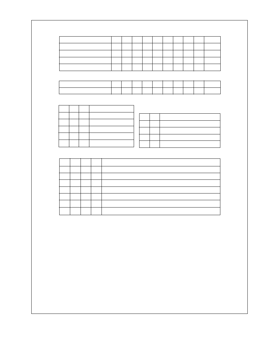
Table 1 Write data format (MSB transmitted first)
Byte 1
Byte 2
Byte 3
Byte 4
Byte 5
Address
Programmable divider
Programmable divider
Charge pump and test bits
I/O port control bits
1
2
14
2
6
CP
P6
0
2
13
2
5
T1
P5
0
2
12
2
4
T0
P4
0
2
11
2
3
TS2
P3
MA0
2
9
2
1
TS0
X
MA1
2
10
2
2
TS1
X
A
A
A
A
A
MSB
1
0
2
7
1
P7
LSB
0
2
8
2
0
OS
P0
Fig. 3 Data formats
A
:
Acknowledge bit
MA1, MA0
:
Variable address bits (see Table 4)
CP
:
Charge Pump current select
T1
:
Test mode selection
T0
:
Charge pump disable
TS2, TS1, TS0
:
Operation mode control bits (see Table 5)
OS
:
Varactor drive Output disable Switch
P7, P6, P5, P4, P3, P0 :
Control output port states
POR
:
Power On Reset indicator
FL
:
Phase lock detect flag
I2, I1, I0
:
Digital information from ports P7, P5 and P4 respectively
A2, A1, A0
:
5-level ADC data from P6 (see Table 3)
X
:
Don't care
Table 2 Read data format
1
POR
1
A0
Byte 1
Byte 2
Address
Status byte
1
FL
0
I2
0
I1
0
I0
MA0
A1
MA1
A2
A
A
Address select input voltage
0V to 0∑2V
CC
Always valid
0∑3V
CC
to 0∑7V
CC
0∑8V
CC
to 13∑2V
Table 3 ADC levels
MA0
0
1
0
1
MA1
0
0
1
1
Table 4 Address selection
Voltage input to P6
0∑6V
CC
to 13∑2V
0∑45V
CC
to 0∑6V
CC
0∑3V
CC
to 0∑45V
CC
0∑15V
CC
to 0∑3V
CC
0V
to 0∑15V
CC
A1
0
1
1
0
0
A2
1
0
0
0
0
A0
0
1
0
1
0
T1
0
0
1
1
1
1
1
TS2
X
X
0
0
1
1
1
TS1
X
X
0
1
0
0
1
TS0
0
1
X
X
0
1
X
Operation mode description
Normal operation, test modes disabled, reference divider ratio = 1024
Normal operation, test modes disabled, reference divider ratio = 512
Charge pump source (down). Status bit FL set to 0
Charge pump sink (up). Status bit FL set to 1
Ports P4, P5, P6, P7set to state X
Port P7 = F
PD
/2; P4, P5, P6 set to state X
Port P7 = F
PD
; P6 = F
COMP
; P4, P5 set to state X
Table 5 Operation modes
NOTES
X = don't care
For further details of test modes, see Table 6
6
SP5655
Fig. 4 Typical application
Fig. 5 Typical input sensitivity
SP5655
9
10
11
12
13
14
15
16
8
7
6
5
4
3
2
1
39n
22k
180n
1n
1
5V
0∑1
µ
BCW31
18p
4MHz
CRYSTAL
1
5V
I
2
C BUS SDA
SCL
CONTROL
MICRO
10n
10k
47k
V
T
1
30V
22k
P3
IF SECTION
AFC OUT
1
12V
IF SIGNAL
1
12V
1n
OSCILLATOR
OUTPUT
VARICAP
INPUT
SATELLITE
TUNER
P0
P4
P5
P6
P7
300
150
100
50
120 1000 2000 2700 3000 3500
FREQUENCY (MHz)
V
IN
(mV RMS INT
O 50
)
OPERATING
WINDOW
7
SP5655
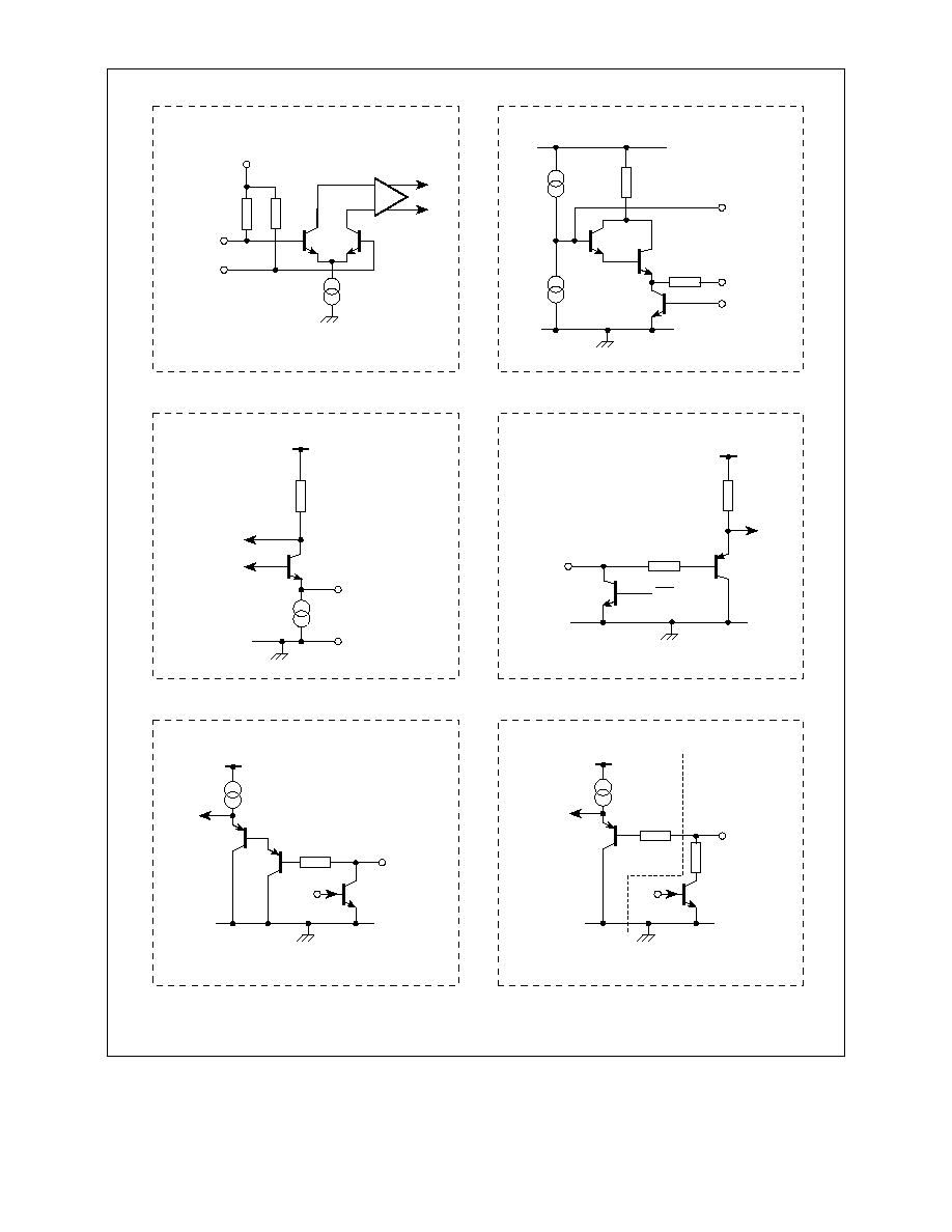
Fig. 6 SP5655 input/output interface circuits
V
REF
RF INPUTS
400
400
150
CHARGE
PUMP
DRIVE
OUTPUT
SCL/SDA
RF input
Loop amplifier
Ports P7-P4
SCL and SDA inputs
Reference oscillator
Ports P0-P3
3k
ACK
*
*
ON SDA ONLY
CRYSTAL Q1
CRYSTAL Q2
OS
(O/P DISABLE)
67k
V
CC
V
CC
V
CC
PORT
V
CC
3k
PORT
3k
V
CC
PORT P3
ONLY
12k
8
SP5655
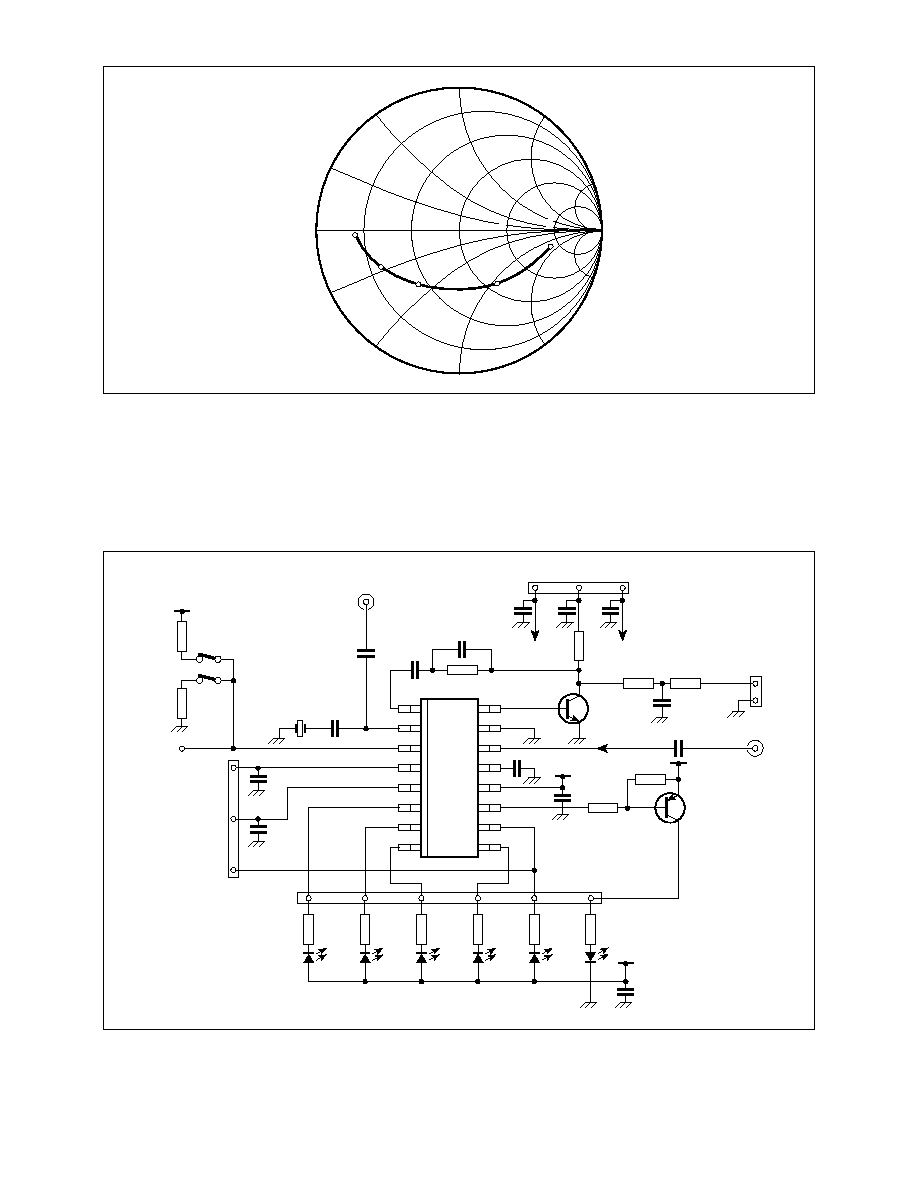
Fig. 7 Typical input impedance,
APPLICATION NOTES
An application note, AN168, is available for designing with
synthesisers such as the SP5655. It covers aspects such as loop
filter design, decoupling and I
2
C bus radiation problems.
The application note is published in the Mitel Semiconductor
Media IC Handbook. A generic test/demonstration board has
been produced, which can be used for the SP5655. A circuit
diagram and layout for the board are shown in Figs. 8 and 9.
The board can be used for the following purposes:
(A) Measuring RF sensitivity perfomance
(B) Indicating port function
(C) Synthesising a voltage controlled oscillator
(D)Testing external reference sources
The programming codes relevant to these tests are given in
Table 6.
Fig. 8 Test board circuit
2∑6GHz
S
11:
Z
O
= 50
NORMALISED TO 50
FREQUENCY MARKER STEP = 500MHz
j 2
j 1
j 0.5
j 0.2
0
2
j 0.2
2
j 0.5
2
j 1
2
j 2
1
0.5
0.2
j 5
2
j 5
2
5
SP5655
1
2
3
4
5
6
7
8
16
15
14
13
12
11
10
9
1
5V
R3 4∑7k
D3
R6 4∑7k
D6
R2 4∑7k
D2
R1 4∑7k
D1
R4 4∑7k
D4
R5 4∑7k
D5
1
5V
1
12V
C10 1n
R13 12k
C4 1n
R14 22k
P4
6
7
8
9
10
11
1
12V
C11
1n
PIN NO.
C5 1n
C3 47n
R7 22k
C2
220n
TR1
2N3904
R9 10k
R10 47k
C14 10n
P3
VAR
GND
TR2
2N3906
C7
100n
C8
100n
C9
100n
1
5V
1
30V
1
12V
P2
R8 22k
C12 100p
C13 100p
P1
DATA/SDA
CLOCK/SCL
ENABLE/ADDRESS SEL
C1
18p
X1
4MHz
EXTERNAL
REFERENCE
SK2
C6 10n
(NOT FITTED,
SEE NOTE)
TP1
S2
S1
R11 3k
R12 1k
SK1
RF INPUT
NOTE
To use an external reference,
capacitor C6 must be fitted
and capacitor C1 removed
from the board.

9
SP5655
Top view (ground plane)
NOTES
1. CIRCUIT SCHEMATIC IS SHOWN IN FIG. 8
2. ALL SUFACE MOUNT COMPONENTS ARE
MOUNTED ON UNDERSIDE OF BOARD
Fig. 9 Test board layout
TP1 = PIN 3 DC BIAS
Underside (surface mounted components side)

10
SP5655
Normal operation, reference divider ratio = 1024
Normal operation, reference divider ratio = 512
Charge pump source (down), FL set to 0
Charge pump sink (up), FL set to 1
Port P7 = F
PD
/2
Port P7 = F
PD
, P6 = F
COMP
Charge pump disable, reference divider ratio = 512
Varactor line disable, reference divider ratio = 512
Charge pump and varactor line disable, reference divider ratio = 512
Operation mode description
Table 5 Operation modes
Hex code (byte 4)
CP high mode
CP low mode
CC
CE
E2
E6
EA
EE
DE
CF
DF
8C
8E
A2
A6
AA
AE
9E
8F
9F
TEST MODES
As explained in the functional description, The SP5655 can
be programmed into a numb er of test modes. These are invoked
by programming Hex codes into byte 4, those most commonly
used being shown in Table 6.
Other codes will also apply due to don't care conditions, which
are assumed to be 1 in the Table.
NOTE:
When looking at F
PD
or F
COMP
signals from ports P7 and P6. byte
should be sent twice, first to set the desired reference division
ratio then to switch on the chosen test mode.
The pulses can then be measured by simply connecting an
oscilloscope or counter to the relevant output pin on the test board.

M Mitel (design) and ST-BUS are registered trademarks of MITEL Corporation
Mitel Semiconductor is an ISO 9001 Registered Company
Copyright 1999 MITEL Corporation
All Rights Reserved
Printed in CANADA
TECHNICAL DOCUMENTATION - NOT FOR RESALE
World Headquarters - Canada
Tel: +1 (613) 592 2122
Fax: +1 (613) 592 6909
North America
Asia/Pacific
Europe, Middle East,
Tel: +1 (770) 486 0194
Tel: +65 333 6193
and Africa (EMEA)
Fax: +1 (770) 631 8213
Fax: +65 333 6192
Tel: +44 (0) 1793 518528
Fax: +44 (0) 1793 518581
http://www.mitelsemi.com
Information relating to products and services furnished herein by Mitel Corporation or its subsidiaries (collectively "Mitel") is believed to be reliable. However, Mitel assumes no
liability for errors that may appear in this publication, or for liability otherwise arising from the application or use of any such information, product or service or for any infringement of
patents or other intellectual property rights owned by third parties which may result from such application or use. Neither the supply of such information or purchase of product or
service conveys any license, either express or implied, under patents or other intellectual property rights owned by Mitel or licensed from third parties by Mitel, whatsoever.
Purchasers of products are also hereby notified that the use of product in certain ways or in combination with Mitel, or non-Mitel furnished goods or services may infringe patents or
other intellectual property rights owned by Mitel.
This publication is issued to provide information only and (unless agreed by Mitel in writing) may not be used, applied or reproduced for any purpose nor form part of any order or
contract nor to be regarded as a representation relating to the products or services concerned. The products, their specifications, services and other information appearing in this
publication are subject to change by Mitel without notice. No warranty or guarantee express or implied is made regarding the capability, performance or suitability of any product or
service. Information concerning possible methods of use is provided as a guide only and does not constitute any guarantee that such methods of use will be satisfactory in a specific
piece of equipment. It is the user's responsibility to fully determine the performance and suitability of any equipment using such information and to ensure that any publication or
data used is up to date and has not been superseded. Manufacturing does not necessarily include testing of all functions or parameters. These products are not suitable for use in
any medical products whose failure to perform may result in significant injury or death to the user. All products and materials are sold and services provided subject to Mitel's
conditions of sale which are available on request.