
SP5730
1.3GHz Low Phase Noise Frequency Synthesiser
Preliminary Information
Description
The SP5730 is a single chip frequency synthesiser
designed for tuning systems up to 1.3GHz and is
optimised for digital terrestrial applications.
The RF preamplifier interfaces direct with the RF
programmable divider, which is of MN+A construction
so giving a step size equal to the loop comparison
frequency and no prescaler phase noise degradation
over the RF operating range.
The comparison frequency is obtained either from an
on-chip crystal controlled oscillator, or from an external
source. The oscillator frequency, Fref, or phase
comparator frequency, Fcomp, can be switched to the
REF/COMP output providing a reference frequency for
a second frequency synthesiser.
The synthesiser is controlled via an I
2
C bus and is fast
mode compliant. It can be hard wired to respond to one
of four addresses to enable two or more synthesisers to
be used on a common bus.
The device contains four switching ports P0-P3.
DS4877
issue 1.9
July 1999
Features
q
Complete 1.3GHz single chip system for
Digital Terrestrial Television applications
q
Selectable reference division ratio, compatible
with (DTT) requirements
q
Optimised for low phase noise, with
comparison frequencies up to 4MHz
q
No RF prescaler
q
Selectable reference/comparison frequency
output
q
Four selectable I
2
C bus address
q
I
2
C fast mode compliant and compatible with
3.3 and 5V logic levels
q
Four switching ports
q
ESD protection, (Normal ESD Handling
procedures should be observed)
Applications
q
Digital Satellite ,Cable and Terrestrial tuning
systems
q
Communications systems
Ordering Information
SP5730A/KG/MP1S Sticks
SP5730A/KG/MP1T Tape and Reel
SP5730A/KG/QP1S Sticks
SP5730A/KG/QP1T Tape amd Reel
2
SP5730
Preliminary Information
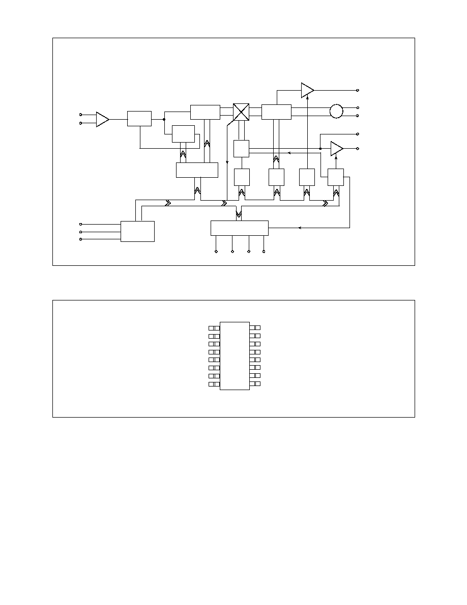
Figure 1 Block diagram
RF INPUT
8/9
3 BIT
COUNT
12 BIT
COUNT
Lock
fpd/2
15 BIT LATCH
PUMP
REF DIVIDER
2 BIT
5 BIT
2 BIT
2 BIT
c/p
mode
enable/select
RF/COMP
CRYSTAL
CRYSTAL CAP
CHARGE PUMP
DRIVE
disable
fpd/2 select
4 BIT LATCH & PORT
INTERFACE
PORT P3 PORT P2 PORT P1PORT P0
I C BUS
TRANSCEIVER
2
ADDRESS
SDA
SCL
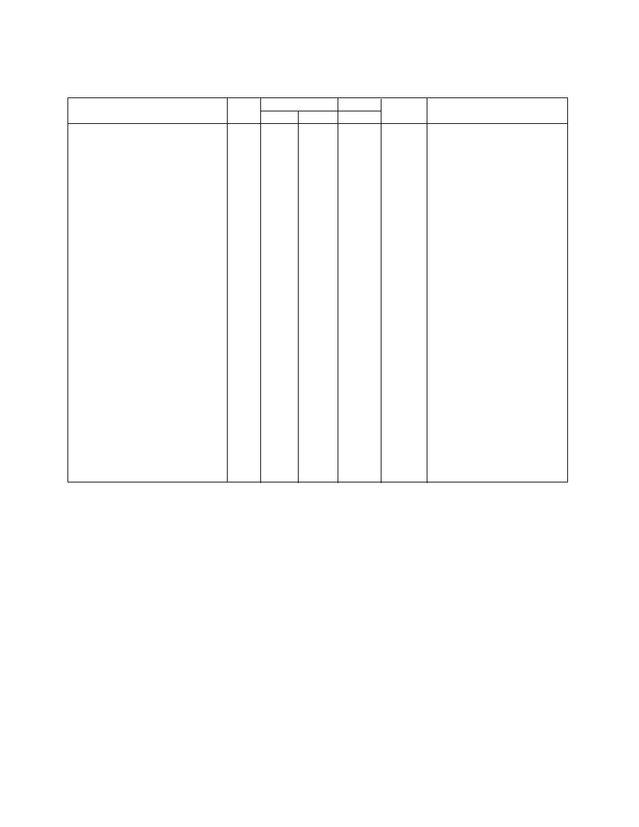
Osc
MP16
SL1711B
1
16
VCCC
AGC
IOUT
VEEA
IFINB
IFIN
IVCCA
QOUT
VEEC
VCCB
VCODIS
VCO
B
VCO
A
VEEB
PSCAL
PSCALB
Figure 2 Pin connections top view
DRIVE
V
EE
RF INPUT
RF INPUT
V
CC
REF/COMP
ADDRESS
PORT P0
CHARGE PUMP
CRYSTAL CAP
CRYSTAL
SDA
SCL
PORT P3/LOGLEV
PORT P2
PORT P1
MP16 & QP16

3
Preliminary Information
SP5730
Electrical Characteristics
Tamb= -40
o
C to 85
o
C, VCC= 4.5 to 5.5V
These characteristics are guaranteed by either production test or design. They apply within the specified
ambient temperature and supply voltage unless otherwise stated.
Characteristic
Pin
Value
Units
Conditions
Min
Typ
Max
Supply current
20
mA
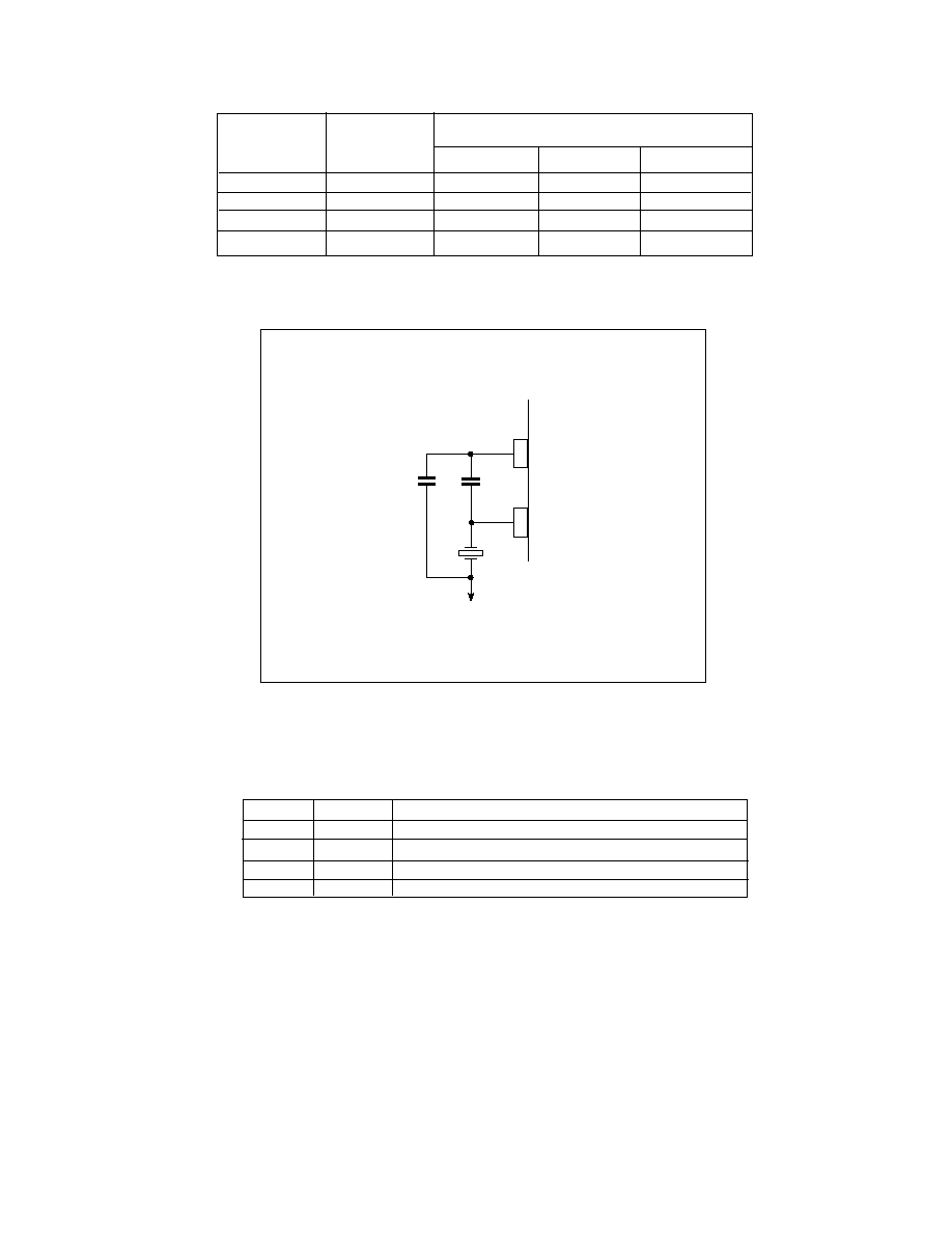
RF input voltage
13,14
12.5
300
mVrms
100 MHz � 1.3GHz, see Figure. 4
RF input voltage
13,14
40
300
mVrms
50MHz - 100MHz, see Figure 4
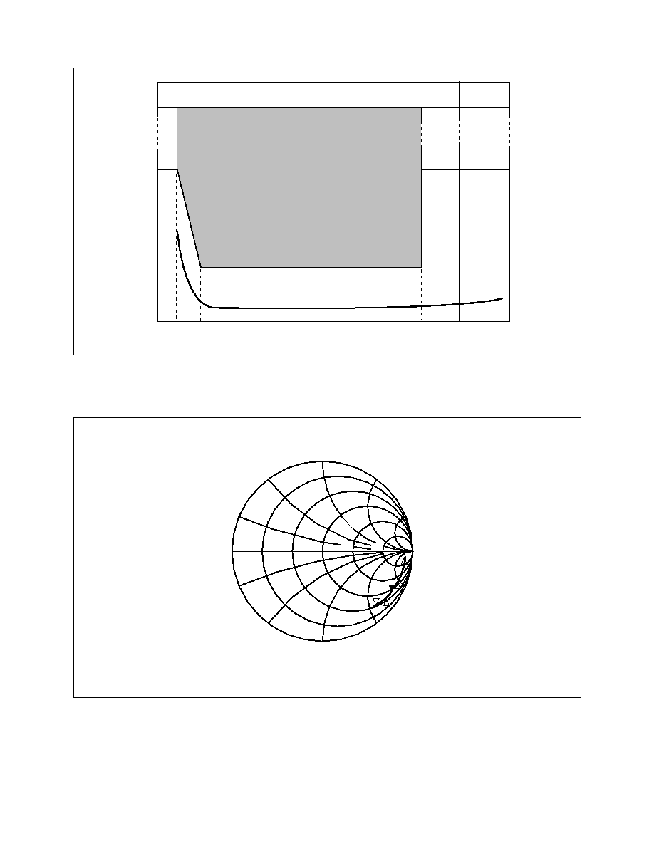
RF input impedance
13,14
See Figure. 5
SDA, SCL
4, 5
Input high voltage
3
5.5
V
5V I
2
C logic selected
Input low voltage
0
1.5
V
5V I
2
C logic selected
Input high voltage
2.3
3.5
V
3V3 I
2
C logic selected
Input low voltage
0
1
V
3V3 I
2
C logic selected
Input high current
10
�
A
Input voltage =Vcc
Input low current
10
�
A
Input voltage = Vee
Leakage current
10
�
A
Vee = Vcc
Hysteresis
0.4
V
SDA output voltage
4
0.4
V
Isink = 3mA
0.6
V
Isink = 6mA
SCL clock rate
5
400
kH
Charge pump output
1
See Table 6 Vpin1 = 2V
current
Charge pump output
1
3
10
nA
Vpin1 = 2V, Vcc = 5V, +25
�
C
leakage
Charge pump drive
16
0.5
mA
Vpin16 = 0.7V
output current
Crystal frequency
2,3
2
20
MHz
See Figure 3 for application
Recommended crystal
10
200
4 MHz "parallel resonant"
series resistance
crystal.
External reference input
3
2
20
MHz
Sinewave coupled through
Frequency
10 nF blocking capacitor
External reference drive
3
0.2
0.5
Vpp
Sinewave coupled through
level
10 nF blocking capacitor
4
SP5730
Preliminary Information
Electrical Characteristics
(continued)
Tamb= -40
o
C to 85
o
C, Vcc= 4.5 to 5.5V
These characteristics are guaranteed by either production test or design. They apply within the specified
ambient temperature and supply voltage unless otherwise stated.
Characteristic
Pin
Value
Units
Conditions
Min
Typ
Max
Buffered REF/COMP output
11
AC coupled 0.5-20MHz
output amplitude
0.35
Vpp
Enabled by bit RE= 1
output impedance
250
See note 2
Phase detector Comparison
4
MHz
frequency
Equivalent phase noise at phase
dBc/Hz
SSB, within loop bandwidth
detector
-152
Fcomp = 2MHz
-158
Fcomp = 125kHz
RF division ratio
56
32767
Reference division ratio
See Table 1
Output ports P0 - P3
6-9
See Note 1
sink current
2
mA
Vport = 0.7
Leakage current
10
�
A
Vport = Vcc
Address Select
10
See Figure 4 Table 3
Input high current
1
mA
Vin = Vcc
Input low current
-0.5
mA
Vin = Vee
Logic level select
6
See note 3
Input high level
3
Vcc
V
5V I
2
C logic selected, or
open circuit
Input low level
0
1.5
V
3V3 I
2
C logic selected
Input current
-10
10
�
A
Vin = Vee to Vcc
Notes:
1. Output ports high impedance on power up, with data, clock, and enable at logic `0'
2. If the REF/COMP output is not used, the output should be left open circuit or connected to Vcc, and disabled by
setting RE = 0
3. Bi-directional port. When used as an output, the input logic state is ignored. When used as an input the port should
be switched in to high impedance (off) state.
5
Preliminary Information
SP5730
Absolute Maximum Ratings
All voltages are referred to Vee at 0V
Characteristic
Min
Max
Units
Conditions
Supply voltage, Vcc
-0.3
7
V
Transient
RF input voltage
2.5
Vpp
Differential
All I/O port DC offsets
-0.3
Vcc+0.3
V
SDA and SCL DC offset
-0.3
6V
V
Storage temperature
-55
+150
o
C
Junction temperature
150
o
C
QP16 thermal resistance,
chip to ambient
80
�
C/W
chip to case
20
�
C/W
Power consumption at
83
mW
All ports off
Vcc = 5.5V
ESD protection
2
kV
mil std 883 latest revision method 3015
class 1
Functional Description
The SP5730 contains all the elements necessary, with
the exception of a frequency reference, loop filter and
external high voltage transistor, to control a varicap
tuned local oscillator, so forming a complete PLL
frequency synthesised source. The device allows for
operation with a high comparison frequency and is
fabricated in high speed logic, which enables the
generation of a loop with good phase noise performance.
It can also be operated with comparison frequencies
appropriate for frequency offsets as required in digital
terrestrial (DTT) receivers The block diagram is shown
in Figure 2.
The RF input signal is fed to an internal preamplifier,
which provides gain and reverse isolation from the
divider signals. The output of the preamplifier interfaces
direct with the 15-bit fully programmable divider, which
is of MN+A architecture, where the dual modulus
prescaler is 8/9, the A counter is 3-bits, and the M
counter is 12 bits.
The output of the programmable divider is fed to the
phase comparator where it is compared in both phase
and frequency domain with the comparison frequency.
This frequency is derived either from the on-board
crystal controlled oscillator or from an external reference
source. In both cases the reference frequency is divided
down to the comparison frequency by the reference
divider which is programmable into 1 of 29 ratios as
detailed in Table 1.
The output of the phase detector feeds a charge pump
and loop amplifier section, which when used with an
external high voltage transistor and loop filter, integrates
the current pulses into the varactor line voltage.
The programmable divider output Fpd divided by two
can be switched to port P0 by programming the device
into test mode. The test modes are described in Table 4.
Programming
The SP5730 is controlled by an I
2
C data bus and is
compatible with both standard and fast mode formats
and with I
2
C data generated from nominal 3.3V and 5V
sources. The I
2
C logic level is selected by the bi-directional
port P3/LOGLEV. 5V logic levels are selected by
connecting P3/LOGLEV to Vcc or leaving open circuit
and 3.3V by connecting to ground. If this port is used as
an input the P3 data should be programmed to high
impedance. If used as an output 5V logic only levels can
be used and in this case the logic state imposed by the
port on the input is ignored.
Data and Clock are fed in on the SDA and SCL lines
respectively as defined by
I
2
C bus format. The synthesiser
can either accept data (write mode), or send data (read
mode). The LSB of the address byte (R/W) sets the
device into write mode if it is low, and read mode if it is
high. Table 2 illustrates the format of the data. The
device can be programmed to respond to several
addresses, which enables the use of more than one
synthesiser in an I
2
C bus system. Table 3 shows how the
address is selected by applying a voltage to the `address'
input.

6
SP5730
Preliminary Information
When the device receives a valid address byte, it pulls
the SDA line low during the acknowledge period, and
during following acknowledge periods after further data
bytes are received. When the device is programmed into
read mode, the controller accepting the data must pull the
SDA line low during all status byte acknowledge periods
to read another status byte. If the controller fails to pull the
SDA line low during this period, the device generates an
internal STOP condition, which inhibits further reading.
Write mode
With reference to Table 2, bytes 2 and 3 contain
frequency information bits 2
14
-2
0
inclusive. Byte 4 and
byte 5 control the reference divider ratio, see Table 1,
charge pump setting, see Table 6, REF/COMP output,
seeTable 7, output ports and test modes, see Table 4.
After reception and acknowledgement of a correct ad-
dress (byte 1), the first bit of the following byte determines
whether the byte is interpreted as a byte 2 or 4, a logic `0'
indicating byte 2, and a logic `1' indicating byte 4. Having
interpreted this byte as either byte 2 or 4 the following
data byte will be interpreted as byte 3 or 5 respectively.
Having received two complete data bytes, additional
data bytes can be entered, where byte interpretation
follows the same procedure, without readdressing the
device. This procedure continues until a STOP condition
is received. The STOP condition can be generated after
any data byte, if however it occurs during a byte transmis-
sion, the previous byte data is retained. To facilitate
smooth fine tuning, the frequency data bytes are only
accepted by the device after all 15 bits of frequency data
have been received, or after the generation of a STOP
condition.
Read mode
When the device is in read mode, the status byte read
from the device takes the form shown in Table 2.
Bit 1 (POR) is the power-on reset indicator, and this is set
to a logic `1' if the Vcc supply to the device has dropped
below 3V (at 25
�
C), e.g. when the device is initially turned
ON. The POR is reset to `0' when the read sequence is
terminated by a STOP command. When POR is set high
this indicates that the programmed information may
have been corrupted and the device reset to power up
condition.
Bit 2 (FL) indicates whether the device is phase locked,
a logic `1' is present if the device is locked, and a logic `0'
if the device is unlocked.
Programmable features
RF programmable
divider
Function as described above
Reference programmable
divider
Function as described above.
Charge pump current
The charge pump current can be pro
grammed by bits C1-C0 within data byte
5, as defined in Table 6.
Test mode
The test modes are invoked by bits REB.
RS, T1 and T0 as described in Table 4.
Reference/Comparison
frequency output
The reference frequency Fref or
comparison frequency Fcomp can be
switched to the REF/COMP output,
function as defined in Table 7.
RE and RS default to logic `I' during
device power up, thus enabling the
comparison frequency Fcomp at the
REF/COMP output.
7
Preliminary Information
SP5730
R4
R3
R2
R1
R0
Ratio
0
0
0
0
0
2
0
0
0
0
1
4
0
0
0
1
0
8
0
0
0
1
1
16
0
0
1
0
0
32
0
0
1
0
1
64
0
0
1
1
0
128
0
0
1
1
1
256
0
1
0
0
0
Illegal state
0
1
0
0
1
5
0
1
0
1
0
10
0
1
0
1
1
20
0
1
1
0
0
40
0
1
1
0
1
80
0
1
1
1
0
160
0
1
1
1
1
320
1
0
0
0
0
Illegal state
1
0
0
0
1
6
1
0
0
1
0
12
1
0
0
1
1
24
1
0
1
0
0
48
1
0
1
0
1
96
1
0
1
1
0
192
1
0
1
1
1
384
1
1
0
0
0
Illegal State
1
1
0
0
1
7
1
1
0
1
0
14
1
1
0
1
1
28
1
1
1
0
0
56
1
1
1
0
1
112
1
1
1
1
0
224
1
1
1
1
1
448
X = don't care
Table 1 Reference division ratio
MSB
LSB
Address
1
1
0
0
0
MA1
MA0
0
A
Byte 1
Programmable divider
0
2
14
2
13
2
12
2
11
2
10
2
9
2
8
A
Byte 2
Programmable divider
2
7
2
6
2
5
2
4
2
3
2
2
2
1
2
0
A
Byte 3
Control Data
1
T1
T0
R4
R3
R2
R1
R0
A
Byte 4
Control Data
C1
C0
RE
RS
P3
P2
P1
P0
A
Byte 5
Table 2 Write data format (MSB is transmitted first)
8
SP5730
Preliminary Information
MSB
LSB
Address
1
1
0
0
0
MA1
MA0
1
A
Byte 1
Status byte
POR
FL
0
0
0
0
0
0
A
Byte 2
Table 2 Read data format (MSB is transmitted first)
A
:
Acknowledge bit
MA1,MA0
:
Variable address bits (see Table 3)
2
14
- 2
0
:
Programmable division ratio control bits
R4-R0
:
Reference division ratio select (see Figure 3)
C1, C0
:
Charge pump current select (see Figure 6)
RE
:
REF/COMP output enable
RS
:
REF/COMP output select when RE=1 (see Figure 2)
T1-T0
:
Test mode control bits
P3-P0
:
P3 - P0 port output states
POR
:
Power on reset indicator
FL
:
Phase lock flag
MA1
MA0
Address input voltage level
0
0
0 - 0.1Vcc
0
1
Open circuit
1
0
0.4Vcc - 0.6Vcc #
1
1
0.9Vcc - Vcc
# Programmed by connecting a 30k
�
5% resistor between pin 10 and Vcc
Table 3 Address selection
RE.RS
T1
T0
Test mode description
0
0
0
Normal operation
1
0
0
Normal operation Port P0 = Fpd/2
X
0
1
Charge pump sink.* Status byte FL set to logic `0'
X
1
0
Charge pump source * Status byte FL set to logic `0'
X
1
1
Charge pump disabled * Status byte FL set to logic `1'
*clocks need to be present on crystal and RF inputs to enable charge pump test modes and to toggle
Status byte bit FL
X = Dont Care
Table 4 Test modes
9
Preliminary Information
SP5730
C1
C0
Current in
�
A
byte 5, bit 1
byte 5, bit 2
Min
Typ
Max
0
0
+- 116
+- 155
+- 194
0
1
+- 247
+- 330
+- 412
1
0
+- 517
+- 690
+- 862
1
1
+- 1087
+- 1450
+- 1812
Table 6 Charge pump current
RE
RS
REF/COMP OUTPUT
0
0
High impedance
0
1
High impedance Test mode enabled, see Figure 5
1
0
Fref selected
1
1
Fcomp selected
X = don't care
Table 7; REF/COMP output
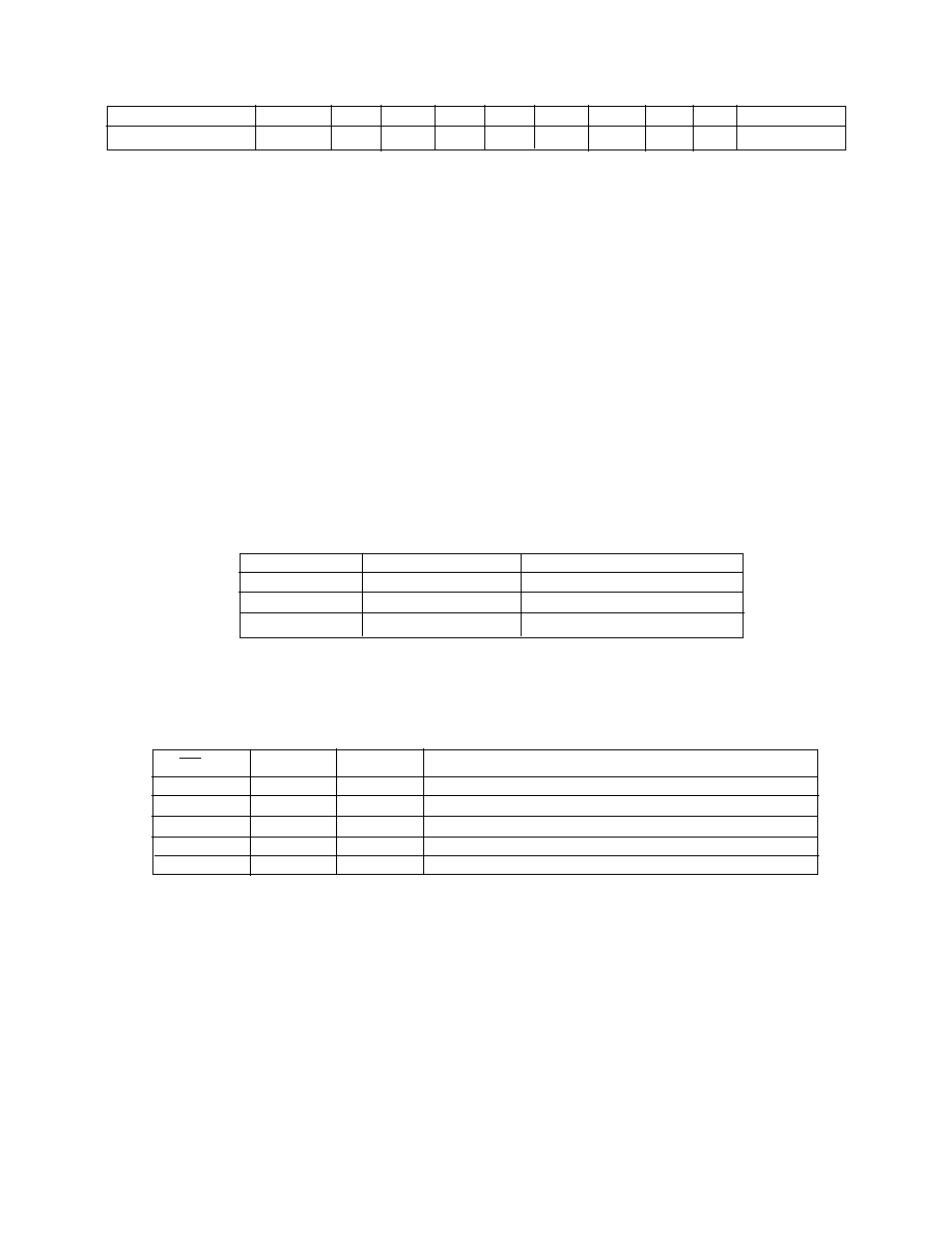
Figure 3 XTAL oscillator application
SP5730
2
3
68pF
150pF
10
SP5730
Preliminary Information
Figure 4 Typical RF input sensitivity
Figure 5 RF input impedance
300
37.5
25
12.5
50
100
500
1000
1300
1500
Frequency (MHz)
0.5
0.2
1
0
+j0.2
+j0.5
+j1
+j2
+j5
2
5
�j5
�j2
�j1
�j0.5
�j0.2
FREQUENCY MARKERS AT 1.3GHz,
X
1.8GHz, 2.3GHz
, 2..8GHz
50MHz, 500Mhz, 1GHz 1.3GHz
11
Preliminary Information
SP5730
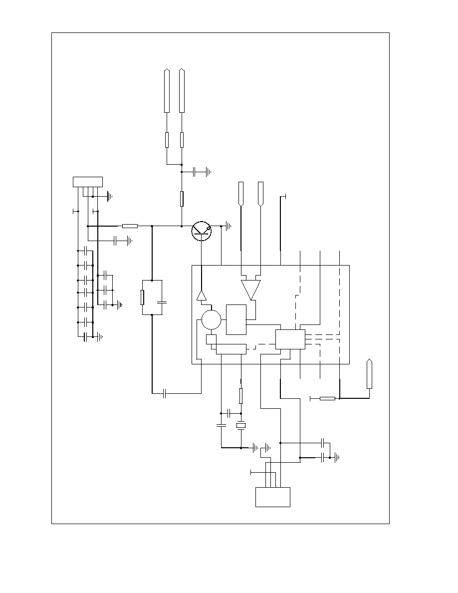
C31
15nF
C32
68pF
R7
13K
T1
BCW31
R8
22K
5V Synth
C30
82pF
X1
4MHz
5V
R9
16K
R10
1K
C39
2.2nF
C41
4u7F
C33
100nF
+5V
+30V
C34
100nF
C38
100pF
C37
100pF
Varactor Line
PSOUT
PSOUTB
R16
10K
LOSEL
5V Synth
C52
4u7F
C51
100pF
C50
100nF
0V
0V
5V Synth
C42
100pF
C43
100nF
C44
100pF
C47
100pF
C49
100nF
C60
150pF
5V Synth
1
2
3
4
5
7
8
9
10
11
12
13
14
15
16
6
RF Input
RF Input
Xtal
Charge Pump
Drive Output
SCL
Address
I2C Bus
Interface
Programmable
Divider
Phase
Comparator
Xtal
Vcc
Ref/Comp
P0
P1
P2
P3/LL
SDA
Vee
Osc
Cap
IC2
SP5769
SDA5
3
5V0
4
GND
5
SCL5
6
J3
I2C BUS
1
2
3
4
5
J1
5 WAY 0.1" HEADER
R19
1K
Varactor Line 2
5V Synth
R20
0R
Figure 6 evaluation board schematic
12
SP5730
Preliminary Information
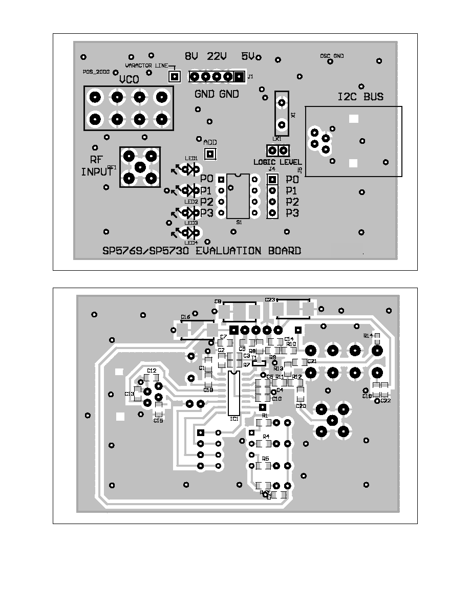
Figure 7 Evaluation board (top view)
Figure 8 Evaluation board (bottom view)

M Mitel (design) and ST-BUS are registered trademarks of MITEL Corporation
Mitel Semiconductor is an ISO 9001 Registered Company
Copyright 1999 MITEL Corporation
All Rights Reserved
Printed in CANADA
TECHNICAL DOCUMENTATION - NOT FOR RESALE
World Headquarters - Canada
Tel: +1 (613) 592 2122
Fax: +1 (613) 592 6909
North America
Asia/Pacific
Europe, Middle East,
Tel: +1 (770) 486 0194
Tel: +65 333 6193
and Africa (EMEA)
Fax: +1 (770) 631 8213
Fax: +65 333 6192
Tel: +44 (0) 1793 518528
Fax: +44 (0) 1793 518581
http://www.mitelsemi.com
Information relating to products and services furnished herein by Mitel Corporation or its subsidiaries (collectively "Mitel") is believed to be reliable. However, Mitel assumes no
liability for errors that may appear in this publication, or for liability otherwise arising from the application or use of any such information, product or service or for any infringement of
patents or other intellectual property rights owned by third parties which may result from such application or use. Neither the supply of such information or purchase of product or
service conveys any license, either express or implied, under patents or other intellectual property rights owned by Mitel or licensed from third parties by Mitel, whatsoever.
Purchasers of products are also hereby notified that the use of product in certain ways or in combination with Mitel, or non-Mitel furnished goods or services may infringe patents or
other intellectual property rights owned by Mitel.
This publication is issued to provide information only and (unless agreed by Mitel in writing) may not be used, applied or reproduced for any purpose nor form part of any order or
contract nor to be regarded as a representation relating to the products or services concerned. The products, their specifications, services and other information appearing in this
publication are subject to change by Mitel without notice. No warranty or guarantee express or implied is made regarding the capability, performance or suitability of any product or
service. Information concerning possible methods of use is provided as a guide only and does not constitute any guarantee that such methods of use will be satisfactory in a specific
piece of equipment. It is the user's responsibility to fully determine the performance and suitability of any equipment using such information and to ensure that any publication or
data used is up to date and has not been superseded. Manufacturing does not necessarily include testing of all functions or parameters. These products are not suitable for use in
any medical products whose failure to perform may result in significant injury or death to the user. All products and materials are sold and services provided subject to Mitel's
conditions of sale which are available on request.