SP8401
Very Low Phase Noise 300MHz
˜
10/11
The SP8401 is a very low phase noise variable modulus
divider. Special circuit techniques have been used to reduce
the phase noise considerably below that produced by standard
dividers. The modulus control input is CMOS or TTL
compatible.
The SP8401 is packaged in a 28 pin plastic SO package to
be compatible with the SP8400 and SP8402 devices.
FEATURES
s
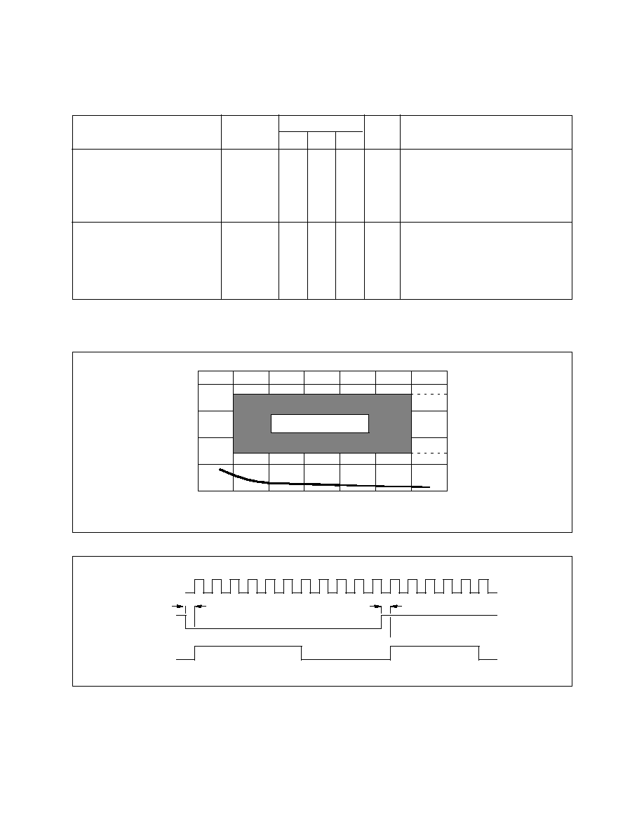
Very low Phase Noise (Typically -160dBc/Hz at 1kHz
offset)
s
Supply Voltage 5V
ABSOLUTE MAXIMUM RATINGS
Supply Voltage
6.5V
Output Current
20mA
Storage Temperature Range
-55
∞
C to +125
∞
C
Maximum Clock Input Voltage
2.5V p-p
ORDERING INFORMATION
SP8401 KG MPES(Commercial Grade)
MP28
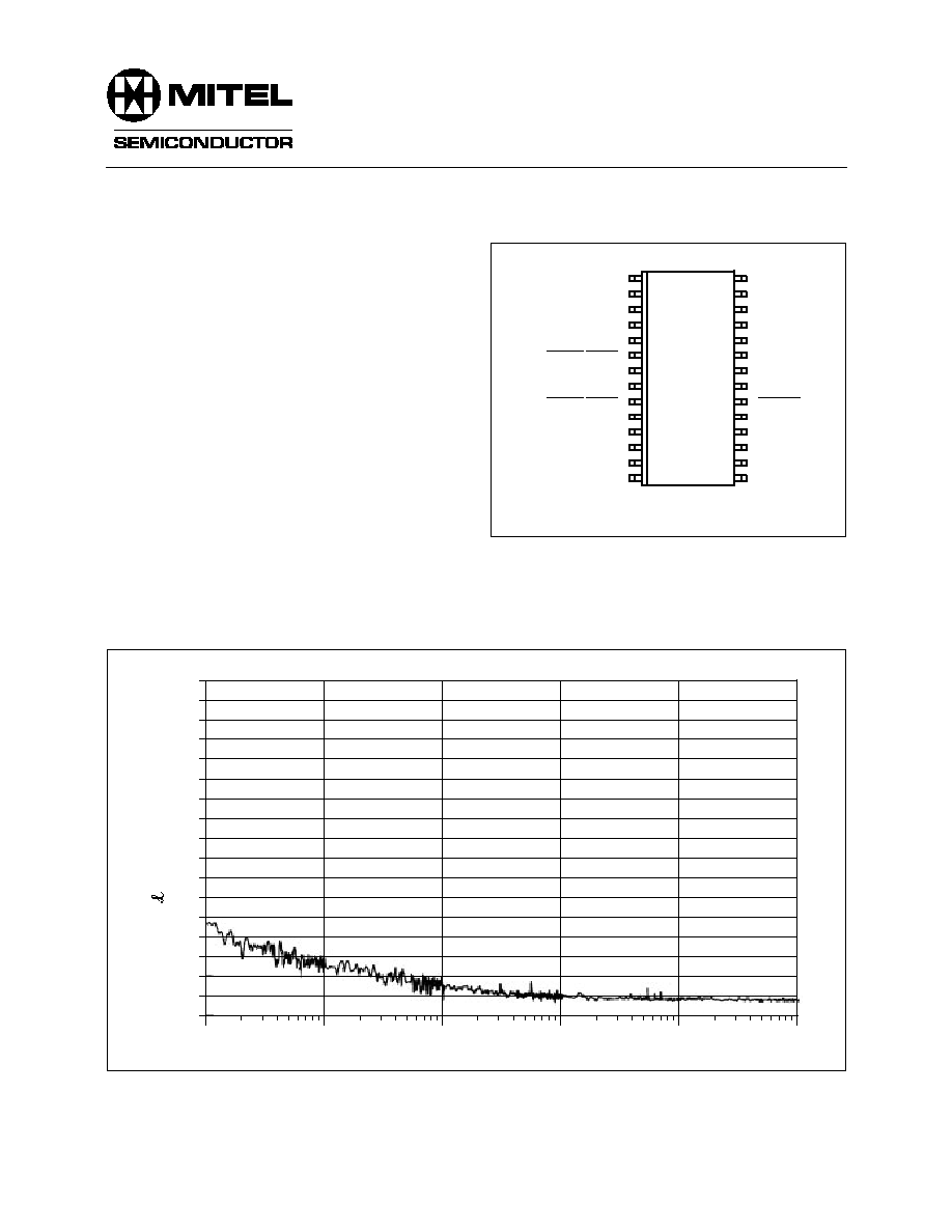
Fig.1 Pin connections - top view
Supersedes February 1992 edition
DS3230 - 3.1 April 1994
1
2
3
4
5
6
7
8
9
10
11
12
13
14
15
16
17
18
19
20
21
22
23
24
25
26
27
28
N/C
N/C
N/C
V
CC
+5V
GND
CLOCK INPUT
CLOCK INPUT
CLOCK INPUT
CLOCK INPUT
GND
V
CC
+5V
V
CC
+5V
N/C
MODULUS CONTROL
N/C
N/C
N/C
N/C
N/C
N/C
N/C
OUTPUT
OUTPUT
N/C
V
CC
+5V
N/C
N/C
N/C
Fig.2 Typical single sideband phase noise measured at 300MHz
(f) (dBc/Hz) ≠3dB
Frequency (Hz)
0
≠10
≠20
≠30
≠40
≠50
≠60
≠70
≠80
≠90
≠100
≠110
≠120
≠130
≠140
≠150
≠160
≠170
1
10
100
1k
10k
100k
2
SP8400
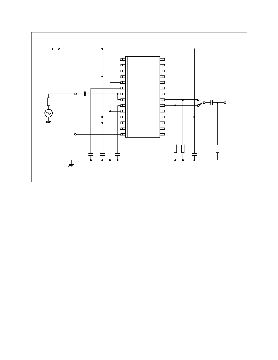
Fig.3 Typical input sensitivity
ELECTRICAL CHARACTERISTICS
Guaranteed over: Supply voltage V
CC
= +4.75V to +5.25V Temperature T
amb
= -10
∞
C to +75
∞
C
Tested at +4.75V and +5.25V at T
amb
= +25
∞
C
Min.
Typ.
Max.
Supply current
Output voltage swing
Input sensitivity 50MHz to 300MHz
Modulus Control Inputs
Logic high voltage
Low low voltage
Input current
Set up time t
s
Release time t
r
57
440
4
4
64
140
(-4)
0.8
180
50
340
2.2
4, 11, 12, 18
20, 21
7, 8
14
14
14
14
14
Output loaded with 300R See Fig.5
p-p @ 330MHz input
˜
11 mode
Output loaded with 300R
RMS Sine wave into 50 Ohms
(dBm equivalent) See Fig.3
˜
10 mode
˜
11 mode
Modulus control input voltage 5V
mA
mV
mV
dBm
V
µ
A
ns
ns
Units
Value
Conditions
Characteristic
Pin
INPUT FREQUENCY (MHz)
400
300
200
100
0
50
100
150
200
250
300
350
355mV
140mV
OPERATING WINDOW
V
IN
mV
RMS
Fig.4 Timing diagram
5
CLOCK INPUT
MODULUS
CONTROL
INPUT
OUTPUT
t
r
t
s
6
5
3
SP8400
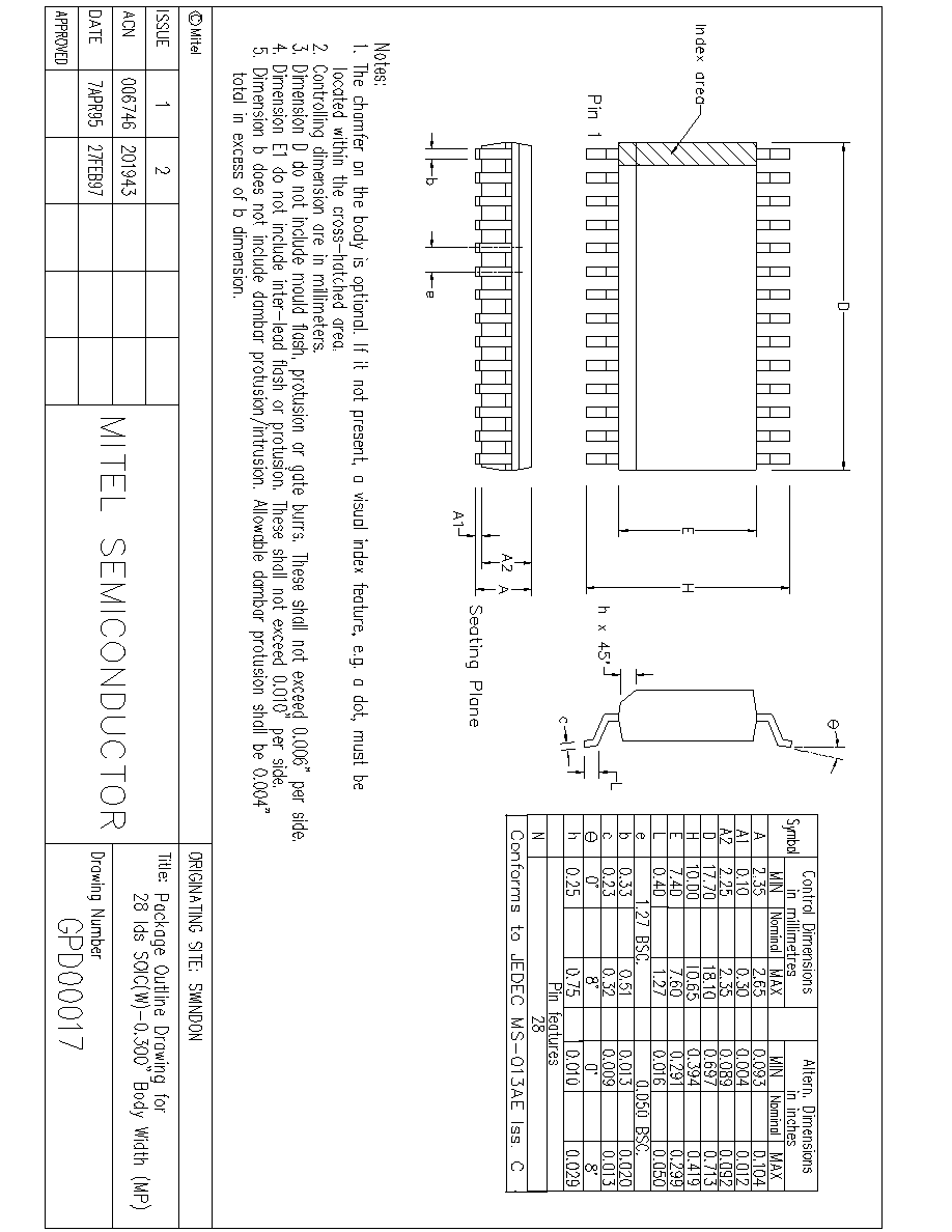
Fig.4 Test circuit
1
2
3
4
5
6
7
8
9
10
11
12
13
14
15
16
17
18
19
20
21
22
23
24
25
26
27
28
SP8401
220nF
10nF
10nF
1nF
1nF
1nF
TTL/CMOS
MODULUS
CONTROL
V
CC
RF
50R
SIGNAL
GENERATOR
2x330R
50R
OUTPUT

M Mitel (design) and ST-BUS are registered trademarks of MITEL Corporation
Mitel Semiconductor is an ISO 9001 Registered Company
Copyright 1999 MITEL Corporation
All Rights Reserved
Printed in CANADA
TECHNICAL DOCUMENTATION - NOT FOR RESALE
World Headquarters - Canada
Tel: +1 (613) 592 2122
Fax: +1 (613) 592 6909
North America
Asia/Pacific
Europe, Middle East,
Tel: +1 (770) 486 0194
Tel: +65 333 6193
and Africa (EMEA)
Fax: +1 (770) 631 8213
Fax: +65 333 6192
Tel: +44 (0) 1793 518528
Fax: +44 (0) 1793 518581
http://www.mitelsemi.com
Information relating to products and services furnished herein by Mitel Corporation or its subsidiaries (collectively "Mitel") is believed to be reliable. However, Mitel assumes no
liability for errors that may appear in this publication, or for liability otherwise arising from the application or use of any such information, product or service or for any infringement of
patents or other intellectual property rights owned by third parties which may result from such application or use. Neither the supply of such information or purchase of product or
service conveys any license, either express or implied, under patents or other intellectual property rights owned by Mitel or licensed from third parties by Mitel, whatsoever.
Purchasers of products are also hereby notified that the use of product in certain ways or in combination with Mitel, or non-Mitel furnished goods or services may infringe patents or
other intellectual property rights owned by Mitel.
This publication is issued to provide information only and (unless agreed by Mitel in writing) may not be used, applied or reproduced for any purpose nor form part of any order or
contract nor to be regarded as a representation relating to the products or services concerned. The products, their specifications, services and other information appearing in this
publication are subject to change by Mitel without notice. No warranty or guarantee express or implied is made regarding the capability, performance or suitability of any product or
service. Information concerning possible methods of use is provided as a guide only and does not constitute any guarantee that such methods of use will be satisfactory in a specific
piece of equipment. It is the user's responsibility to fully determine the performance and suitability of any equipment using such information and to ensure that any publication or
data used is up to date and has not been superseded. Manufacturing does not necessarily include testing of all functions or parameters. These products are not suitable for use in
any medical products whose failure to perform may result in significant injury or death to the user. All products and materials are sold and services provided subject to Mitel's
conditions of sale which are available on request.