
1
SP8715
SP8715
1100MHz Very Low Current Multi-Modulus Divider
Description
The SP8715 is a switchable divide by 64/65, 128/129
programmable divider which is guaranteed to operate up
to 1100MHz. It will operate from a supply of 2.7V to 5.25V
and requires typically 3.6mA (including the output current).
It also features a power down facility for battery economy.
The RF inputs are internally biased and should be
capacitively coupled to the signal source. The output is
designed to interface with CMOS synthesisers.
Features
G
Operation to 1100MHz
G
Very Low Power
G
Single Supply Operation 2.7V to 5.25V
G
Power Down Facility for Battery Economy
G
Latched Modulus Control Input
G
Push Pull Output Drive
G
ESD Protection on All Pins
DS3830
Issue 4.2
September 1999
Applications
G
Cellular Telephones
G
Cordless Telephones
G
Mobile Radio
ESD precautions must be observed
Odering Information
SP8715/IG/MPAS Industrial Temperature Range
Miniature Plastic SOIC Package
SP8715/IG/MPAC As Above supplied on Tape
and Reel
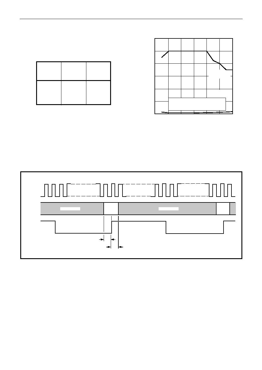
BIAS
V
CC
2
7
5
250K
NOMINAL
4
CK
D
Q
6
3
V
CC
V
EE
1
8
V
EE
POWER
DOWN
OUTPUT
MC
RS
RF
INPUT
(CLOCK)
DIVIDE BY
4 / 5
DIVIDE BY
16 / 32
CONTROL
LOGIC
D TYPE
Figure 1 Block Diagram

2
SP8715
Figure 2 Pin Connections
MP8
Absolute Maximum Ratings
Supply voltage (V
EE
=0V)
(note 1)
-0.5V to 7V
Control and RF inputs,
RF output (V
EE
=0V)
(note 1)-0.5V to V
CC
+0.5V
RF input current
(note 1)
10mA
Operating temperature
-40
�C to +85�C
Storage temperature range
-55
�C to +150�C
Maximum junction temperature
+150
�C
NOTE 1. Duration <2 minutes.
Electrical Characteristics
Guaranteed over the following conditions (unless otherwise stated):
V
CC
=+2.7V to +5.25V (with respect to V
EE
), Output load (pin 4) = 10pF, T
amb
= -40
�C to +85�C (note 2)
Characteristic
Units
Conditions
Supply current
(note 3)
3.6
4.2
mA
Power down input low
Supply current
(note 3)
8
50
�A
Power down input high
Power down high
V
CC
-0.5
V
CC
V
Power down low
0
V
CC
-2.0
V
Modulus control high
(note 4)
0.6V
CC
V
CC
V
Divide by 64 or 128
Modulus control low
(note 4)
0
0.4V
CC
V
Divide by 65 or 129
Ratio select high
(note 4, 9)
0.6V
CC
V
CC
V
Divide by 64 or 65
Ratio select low
(note 4, 9)
0
0.4V
CC
V
Divide by 128 or 129
Max. sinewave input frequency
1100
MHz
See Figure 5
Min. sinewave input frequency
200
MHz
See Figure 5
Min. RF input voltage
50
mV RMS RF input 200MHz to
1100MHz. See Figure 5
Max. RF input voltage
200
mV RMS RF input 200MHz to
1100MHz. See Figure 5
Value
Min.
Typ.
Max.
3
SP8715
Electrical Characteristics (Continued)
Guaranteed over the following conditions (unless otherwise stated):
V
CC
=+2.7V to +5.25V (with respect to V
EE
), Output load (pin 4) = 10pF, T
amb
= -40
�C to +85�C (note 2)
Characteristic
Units
Conditions
Output level (pin 4)
500
600
mV p-p
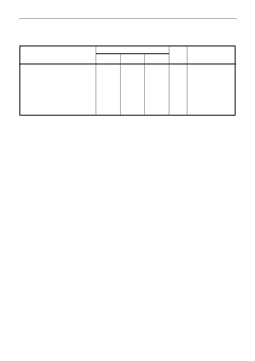
Modulus set-up time, t
s
(notes 5,6,8)
20
ns
RF input = 1GHz
Modulus hold time, t
h
(notes 6,8)
1
ns
RF input = 1GHz
Power down time, t
pd
(notes 7,8)
10
�s
See Figure 9
Power down recovery time, t
pu
6
�s
See Figure 9
(notes 7,8)
NOTES
2.
All electrical testing is performed at +85
�C.
3.
Typical values are measured at +25
�C and V
CC
= +5V.
4.
Modulus Control and Ratio Select are high impedance inputs which can be driven directly by standard
CMOS outputs.
5.
Modulus control is latched at the end of the previous cycle.
6.
See Figure 4.
7.
See Figure 8.
8.
These parameters are not tested but are guaranteee by design.
9.
The ratio select pin is not intended to be switched dynamically.
Value
Min.
Typ.
Max.
OPERATING NOTES
The RF inputs are biased internally and are normally
coupled to the signal source with suitable capaitors.
The output stage has a novel design and is intended
to drive a CMOS synthesiser input. External pull-down
resistors or circuits are not required. The SP8715 is
not suitable for driving TTL or similar devices.
The device will operate down to DC frequencies for
non-sinusoidal signals provided that the input slew
rate is better than 100V/
�s.
POWER DOWN (pin 7) is connected internally to a
pull-down resistor. If the battery economy facility is not
used, pin 7 should be either left unconnected or
connected to V
EE
.
4
SP8715
Thi
h
t
i
l t
l
id Th
l
Figure 3 Typical Input Characteristics
Ratio
Modulus
Division
Select
Control
Ratio
(Pin 3)
(Pin 6)
L
L
129
L
H
128
H
L
65
H
H
64
TYPICAL
SENSITIVITY
TYPICAL
OVERLOAD
1000
800
600
400
200
0
200 400 600 800 1000 1200
* Tested as specified in table of Electrical Characteristics
FREQUENCY (MHZ)
RF INPUT VOLTAGE (mV RMS)
GUARANTEED*
OPERATING WINDOW
Table 1 Truth Table
Figure 4 Modulus Control Timing Diagram
RF INPUT
CLOCK
MODULUS
CONTROL
INPUTS
OUTPUT
t s
t h
32 (64)
32 (64) or 33 (65)
DON'T CARE
DON'T CARE
5
SP8715
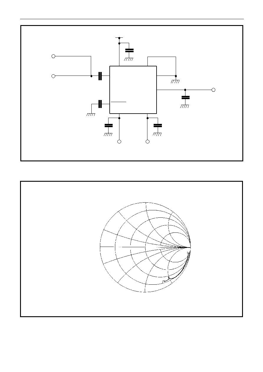
Figure 5 Toggle Frequency Test Circuit
Figure 6 Typical S11 parameter for pin 1. V
CC
= +5.0V
j0.2
j0.5
j1
S11
PLOT 50 OHM
NORMALISED
f1: 130MHz
f2: 1310MHz
j2
-j0.2
-j0.5
-j2
-j1
f1
f2
0.2
0.5
1
2
VCC
V CC
RF INPUT
POWER
DOWN
RATIO
SELECT
MC
RF INPUT
OUTPUT
MODULUS
CONTROL 1 INPUT
1n
1n
10n
10n
100n
C L
50
MONITOR
50
SIGNAL
SOURCE
SP8715
OUTPUT
MODULUS
CONTROL 2 INPUT
V EE