 | –≠–ª–µ–∫—Ç—Ä–æ–Ω–Ω—ã–π –∫–æ–º–ø–æ–Ω–µ–Ω—Ç: SP8852 | –°–∫–∞—á–∞—Ç—å:  PDF PDF  ZIP ZIP |
SP8852E
2∑7GHz Parallel Load Professional Synthesiser
Preliminary Information
Supersedes January 1996 version, DS4237 - 1.2
DS4237 - 2.0 June 1998
The SP8852E is one of a family of parallel load synthesisers
containing all the elements apart from the loop amplifier to
fabricate a PLL synthesis loop. Other parts in the series are
the SP8854E which has hard wired reference counter pro-
gramming and requires only a single 16-bit programming
word, and the SP8855E which is fully programmable using
hard wired links or switches.
The SP8852E is programmed using a 16-bit parallel data
bus. Data can be stored in one of two internal buffers, selected
by a single address bit on the input interface. In order to fully
program the device, two 16-bit words are required, one to
select the RF division ratio (A and M counters) and phase
detector gain, and one to set the 10-bit reference divider
count, phase detector state and sense. Once the reference
divide ratio has been set, frequency changes can be made by
a single 16-bit data load entry to the RF divider chain.
*F
PD
and F
REF
outputs are reversed by the phase
detector sense bit in the F1/F2 programming word, bit
12. The above diagram is correct when bit 12 is high.
HC44
FEATURES
s
2∑7 GHz Operating Frequency
s
Single 5V Supply
s
Low Power Consumption <1∑3W
s
High Comparison Frequency : 20MHz
s
High Gain Phase Detector : 1mA/rad
s
Zero `Dead Band' Phase Detector
s
Wide Range of RF and Reference Division Ratios
s
Programming by Dual Word Data Transfer
ABSOLUTE MAXIMUM RATINGS
Supply voltage
Operating temperature
Storage temperature
Prescaler and reference input voltage
Data inputs
Junction temperature
2
0∑3V to 16V
2
55
∞
C to1100
∞
C
2
65
∞
C to 1150
∞
C
2∑5Vp-p
V
CC
10∑3V
V
EE
20∑3V
1
175
∞
C
ORDERING INFORMATION
SP8852E KG HCAR Non-standard temperature range,
2
55
∞
C to
1
100
∞
C, standard product screening
SP8852E IG HCAR Industrial temperature range,
2
40
∞
C to
1
85
∞
C, standard product screening
THERMAL DATA
u
JC
= 5
∞
C/W
u
JA
= 53
∞
C/W
ESD PROTECTION
1000V, human body model
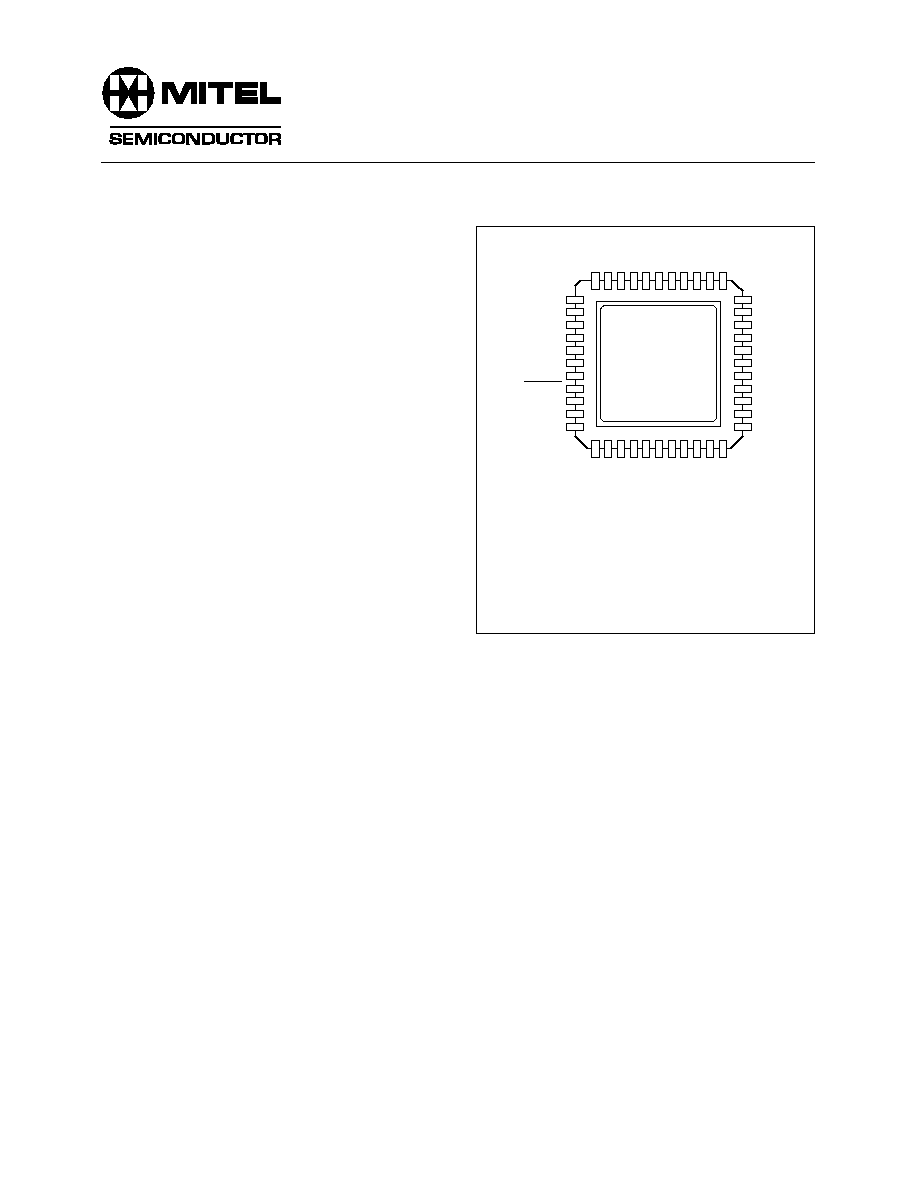
Fig. 1 Pin connections - top view
1 44
B4
B3
B2
B1
B0
0V (PRESCALER)
RF INPUT
RF INPUT
V
CC
(PRESCALER)
VEE
LOCK DETECT
STROBE
ADDRESS
NC
NC
NC
NC
NC
NC
NC
NC
NC
C-LOCK DETECT
R
SET
CHARGE PUMP
OUTPUT
CHARGE PUMP
REF
NC
NC
F
PD
*
F
REF
*
V
CC
REF OSC CAP
ACIT
OR
REF IN/CR
YST
AL
B5
B6
B7
B8
B9
B10
B1
1
B12
B13
B14
B15
SP8852E

2
SP8852E
Fig. 2 Block diagram
STROBE
ADDRESS
B0
B1
B2
B3
B4
B5
B6
B7
B8
B9
B10
B11
B12
B13
B14
B15
39
38
11
10
9
8
7
6
5
4
3
2
1
44
43
42
41
40
INPUT
INTERFACE
4
8/9
13
14
15
14
V
CC
PRESCALER
RF INPUT
0V
PRESCALER
3-BIT
A COUNTER
11-BIT
M COUNTER
B0
B2
B3
B13 B14
B15
LOAD
RF BUFFER
PHASE
DETECTOR
REFERENCE BUFFER
LOAD
10-BIT REFERENCE
DIVIDER
B0
B9
B10
B12
F
REF
F
PD
REFERENCE
CRYSTAL
REFERENCE
CAPACITOR
28
27
CHARGE PUMP OUTPUT
CHARGE PUMP REFERENCE
LOCK DETECT OUTPUT
R
SET
C-LOCK DETECT
F
PD
*
F
REF
*
V
CC
V
EE
MODULUS
CONTROL
*FREF and FPD outputs are reversed
by the phase detector sense bit, bit 12
in the programming word. The pin
allocations shown are correct when
bit 12 is high.
20
21
17
19
18
24
25
26
16
RF INPUT

3
SP8852E
Pin
1-11, 40-44
13 (RF INPUT)
14 (RF INPUT)
17 (LOCK DETECT INPUT)
18 (C-LOCK DETECT)
19 (R
SET
)
20 (CHARGE PUMP OUTPUT)
21 (CHARGE PUMP REF)
22
23
24
F
PD
if pin 23 is high
F
REF
if pin 23 is low
25
F
PD
if pin 23 is low
F
REF
if pin 23 is high
27 (Ref. oscillator capacitor)
28 (REF IN/XTAL)
29-37
38 (ADDRESS)
39 (STROBE)
Description
These are the inputs to the 16-bit data bus. When pin 38 is high the data goes to the buffers for
the A counter, M counter and phase detector gain. When pin 38 is low the data goes to the buffers
for the reference counter and the phase detector state (see Table 4). Open circuit = 1 (high) on
these pins. Data is transparent from pins to the selected buffers when pin 39 (STROBE) is high
and frozen in buffers when pin 39 is low.
Balanced inputs to the RF preamplifier. For single-ended operation the signal is AC-coupled into
pin 13 with pin 14 AC-decoupled to ground (or vice-versa). Pins 13 and 14 are internally DC
biased.
A current sink into this pin is enabled when the lock detect circuit indicates lock. Used to give
an external indication of phase lock.
A capacitor connected to this point determines the lock detect integrator time constant and can
be used to vary the sensitivity of the phase lock indicator.
An external resistor from pin 19 to V
CC
sets the charge pump output current.
The phase detector output is a single ended charge pump sourcing or sinking current to the
inverting input of an external loop filter. The direction is controlled by bit 12 of the reference word.
For bit 12 = 1 and F
PD
or RF phase leads Ref phase pin 20 will sink current (see Table 3).
Connected to the non-inverting input of the loop filter to set the optimum DC bias.
Not Connected.
Not connected.
RF divider output pulses. F
PD
= RF input frequency/(M.N
1
A). Pulse width = 8 RF input cycles
(1 cycle of the divide by 8 prescaler output).
Reference divider output pulses. F
REF
= reference input frequency/R. Pulse width = high period
of Ref input.
Leave open circuit if an external reference is used. See Fig. 5 for typical connection for use as
an onboard crystal oscillator.
This pin is the input buffer amplifier for an external reference signal. This amplifier provides the
active element if an onboard crystal oscillator is used.
Not connected.
Controls which buffer the data on the input bus goes to. Pin 38 high sends data to the RF divider
group of functions. Pin 38 low sends data to the Ref divider group of functions (see Fig. 6). Open
circuit = high.
When pin 39 is high the A, M, and R counters are held in the reset state and the charge pump
output is disabled. The data on the input bus is loaded into the buffers selected by the ADDRESS
input state (pin 38) when pin 39 goes low. When pin 39 is low the data is fixed in the buffers, the
buffers are loaded into the counter and control register, all the counters are active, and the
charge pump is enabled. Open circuit = high.
Table 1 Pin descriptions

4
SP8852E
ELECTRICAL CHARACTERISTICS
The Electrical Characteristics are guaranteed over the following range of operating conditions unless otherwise stated
T
AMB
=
2
55
∞
C to
1
100
∞
C (KG parts),
2
40
∞
C to
1
85
∞
C (IG parts); V
CC
= 4∑75V to 5∑25V
Characteristic
Conditions
Supply current
RF input sensitivity
RF division ratio
Reference division ratio
Comparison frequency
Reference input frequency
Reference input voltage
F
REF
/F
PD
output voltage high
F
REF
/F
PD
output voltage low
LOCK DETECT output voltage
CHARGE PUMP current
Input bus logic level high
Input bus logic level low
Input bus current source
Input bus current sink
Up/down current matching
CHARGE PUMP REFERENCE voltage
R
SET
current
R
SET
voltage
C-LOCK DETECT current
STROBE pulse width
Data setup time
2
5
56
1
10
0
6
1∑4
6
2∑0
6
3∑4
6
5∑4
3∑5
2
200
V
CC
2
1∑6
0∑5
50
100
240
1
7
16383
1023
50
100
1
10
500
6
1∑7
6
2∑5
6
4∑1
6
6∑5
1
10
6
5
V
CC
2
0∑5
2
180
1
6
2
0∑8
2
1∑4
300
6
1∑5
6
2∑3
6
3∑8
6
6∑1
1∑6
1
10
Pin
18, 26
13,14
13,14, 24
28, 25
28, 24, 25
28
28
24, 25
24, 25
17
19, 20, 21
1-11, 38-44
1-11, 38-44
1-11, 38-44
1-11, 38-44
20
21
19
19
18
Typ.
Max.
Min.
mA
dBm
MHz
MHz
dBm
V
V
mV
mA
mA
mA
mA
V
V
µ
A
µ
A
%
V
V
mA
V
µ
A
ns
ns
Units
Value
100MHz to 2∑7GHz. See note 3.
Ref division ratio >2. See note 1
WRT V
CC
, 2∑2k
to 0V
WRT V
CC
, 2∑2k
to 0V
I
OUT
= 3mA
V
PIN20
= V
PIN21
, I
PIN19
= 1∑6mA,
multiplication factor = 1
V
PIN20
= V
PIN21
, I
PIN19
= 1∑6mA,
multiplication factor = 1∑5
V
PIN20
= V
PIN21
, I
PIN19
= 1∑6mA,
multiplication factor = 2∑5
V
PIN20
= V
PIN21
, I
PIN19
= 1∑6mA,
multiplication factor = 4∑0
V
IN
= 0V
V
IN
= V
CC
V
PIN20
= V
PIN21
, I
PIN19
= 1∑6mA
I
PIN19
= 1∑6mA, current
multiplication factor = 1∑0
I
PIN19
= 1∑6mA, current
multiplication factor = 4∑0
Note 2
I
PIN19
= 1∑6mA
V
PIN18
= 4∑7V
Note 3
Note 3
NOTES
1. Lower frequencies may be used provided that slew rates are maintained.
2. Pin 19 current
3
multiplication factor must be less than 5mA if charge pump accuracy is to be maintained.
3. Guranteed but not tested.
5
SP8852E
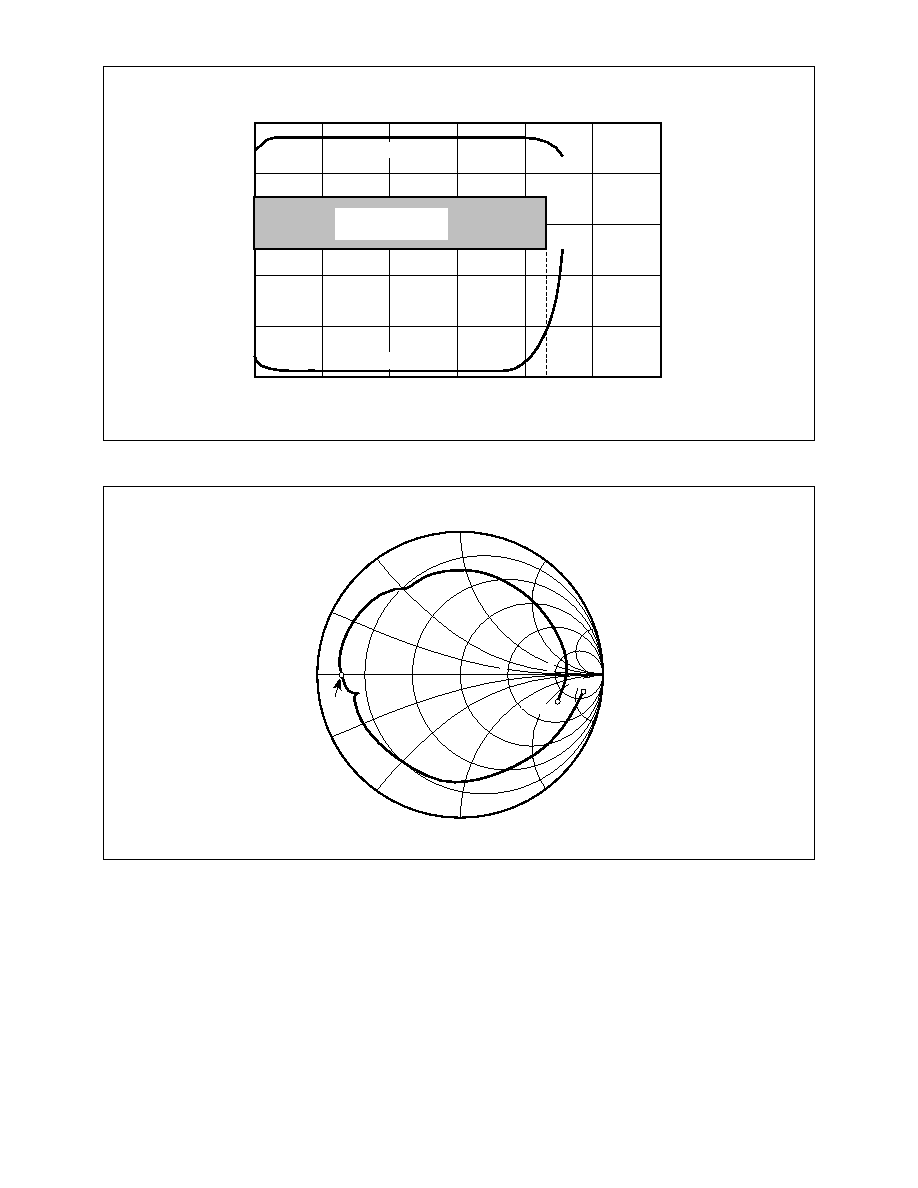
1
20
1
10
1
7
0
2
5
2
10
2
20
2
30
100MHz
FREQUENCY
RF INPUT T
O
PIN 13 (dBm)
1GHz
2GHz 2∑7GHz
10GHz
GUARANTEED
OPERATING WINDOW
TYPICAL SENSITIVITY
TYPICAL OVERLOAD
Fig. 3 Input sensitivity
1∑1GHz
Z
O
= 50
j 2
j 1
j 0.5
j 0.2
0
2
j 0.2
2
j 0.5
2
j 1
2
j 2
1
0.5
0.2
j 5
2
j 5
2
5
2∑5GHz
50MHz
Fig. 4 RF input impedance
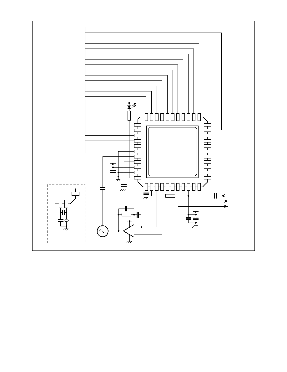
6
SP8852E
1
5V
1k
-
+
1
44
SP8852E
7
8
9
10
11
12
13
14
15
16
17
2
3
4
5
6
43 42 41 40
23 24
22
21
20
19
18
25 26 27 28
39
38
37
36
35
34
33
32
31
30
29
F
PD
1n
REF IN
F
REF
1
5V
1
µ
10n
2∑2k
100p
1
5V
1n
1n
1n
VCO
LOOP FILTER
1
30V
SP8852E
27
28
33p
100p
10MHZ
Application using
crystal reference
CONTROL
MICRO
ADDRESS
STROBE
VALUES DEPEND
ON APPLICATION
OP27
ETC
*
*
*
*
Fig. 5 Typical application diagram
DESCRIPTION
Prescaler and
AM counter The programmable divider
chain is of
A and M counter construction and therefore
contains a dual modulus front end prescaler, an
A counter
which controls the dual modulus ratio and an
M counter which
performs the bulk multi-modulus division. A programmable
divider of this construction has a division ratio of
MN
1
A and
a minimum integer steppable division ratio of
N(N
2
1), where
N is the prescaler value.
Data Entry and Storage
Data is loaded from the 16-bit bus into one of the internal
buffers by applying a positive pulse to the STROBE input. The
input bus can be driven from TTL or CMOS logic levels. When
STROBE is low, the inputs are isolated and the data can be
changed without affecting the programmed state.
The data is loaded into the RF buffer when the address
input is high and into the reference buffer when low. When the
STROBE input is taken high, the
A and M and reference
counters are reset and the input data is applied to the internal
storage register. When STROBE is again taken low, the data
on the input bus is stored in the selected register and the
counters released. The STROBE input is level triggered so
that if the data is changed whilst the input is high, the final
value before STROBE goes low will be stored.
In order to prevent disturbances on the VCO control voltage
when frequency changes are made, the STROBE input disables

7
SP8852E
the charge pump outputs when high. During this period the
VCO control voltage will be maintained by the loop filter
components around the loop amplifier, but due to the com-
bined effects of the amplifier input current and charge pump
leakage a gradual change will occur. In order to reduce the
change, the duration of the strobe pulse should be minimised.
Selection of a loop amplifier with low input current will reduce
the VCO voltage droop during the strobe pulse and result in
minimum reference sidebands from the synthesiser.
Reference Input
The reference source can be either driven from an external
sine or square wave source of up to 100MHz or a crystal can
be connected as shown in Fig. 5.
Phase Comparator and Charge Pump
The SP8852E has a digital phase/frequency comparator
driving a charge pump with programmable current output.
The charge pump current level at the minimum gain setting is
approximately equal to the current fed into the R
SET
input, pin
19, and can be increased by programming the bus according
to Table 2 by up to 4 times.
V
CC
2
1∑6V
R
SET
Pin 19 current =
Phase detector gain =
I
PIN19
(mA)
3
multiplication factor
2
p
mA/rad
Sense bit (bit 12)
1
0
Pin 20
Current source
Current sink
Output for RF phase lag
Table 3
Bit 11
0
0
1
1
Bit 10
0
1
0
1
Phase detector state
Enabled, F
PD
and F
REF
off
Enabled, F
PD
and F
REF
on
Disabled by lock detect, F
PD
and F
REF
on
Disabled, F
PD
and F
REF
on
The charge pump connections to the loop amplifier consist
of the charge pump output and the charge pump reference.
The matching of the charge pump up and down currents will
only be maintained if the charge pump output is held at a
voltage equal to the charge pump reference using an
operational amplifier to produce a virtual earth condition at pin
20. The lock detect circuit can drive an LED to give visual
indication of phase lock or provide an indication to the control
system if a pullup resistor is used in place of the LED. A small
capacitor connected form the C-LOCK DETECTOR pin to
ground may be used to delay lock detect indication and
remove glitches produced by momentary phase coincidence
during lock up.
To allow for control direction changes introduced by the
design of the PLL, bit 12 on the input bus address 0 can be
programmed to reverse the sense of the phase detector by
transposing the F
PD
and F
REF
connections. In order that any
external phase detector will also be reversed by this program-
ming bit, the F
PD
and F
REF
outputs are also interchanged by
bit 12 as shown in Table 3.
2
11
2
10
2
9
2
8
2
7
2
6
2
5
2
4
2
3
2
2
2
1
2
0
2
12
2
13
1
2
9
2
8
2
7
2
6
2
5
2
4
2
3
2
2
2
1
2
0
0
ADDRESS
PIN 40
BIT 15
PIN 11
BIT 0
NOT USED
PHASE
DETECTOR
STATE
CONTROL
(SEE TABLE 4)
PHASE
DETECTOR
SENSE
CONTROL
(SEE TABLE 3)
10-BIT REFERENCE COUNTER
Fig. 6a Reference word bit allocation
ADDRESS
PHASE
DETECTOR
GAIN
CONTROL
(SEE TABLE 2)
M COUNTER
3-BIT
A COUNTER
Fig. 6b RF division ratio bit allocation
PIN 40
BIT 15
PIN 11
BIT 0
Fig. 6 Programming data format
Bit 15
0
0
1
1
Bit 14
0
1
0
1
Current multiplication factor
1∑0
1∑5
2∑5
4∑0
Table 2
Table 4
The F
PD
and F
REF
signals to the phase detector are
available on pins 24 and 25 and may be used to monitor the
frequency input to the phase detector or used in conjunction
with an external phase detector. These outputs may be
programmed by bits 10 and 11 of word 0 according to Table 4.
State 3, where the outputs are disabled by the lock detect
circuit, is useful where the user wishes to use an external
phase detector. The internal phase/frequency detector may
be used to pull the loop into lock and an automatic switch-over
to the external phase detector made. When the F
PD
and F
REF
outputs are to be used at high frequencies, an external pull
down resistor of minimum value 330
may be connected to
ground to reduce the fall time of the output pulse.
8
SP8852E
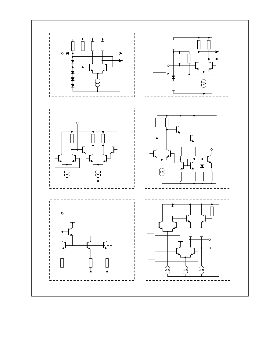
500
500
4k
325
325
3mA
13
14
RF INPUT
RF INPUT
V
CC
0V
3k
Fig. 7a 16-bit input bus, strobe and address
Fig. 7b RF inputs
5k
50
µ
A
INPUT
5k
V
CC
0V
40k
40k
Fig. 7c Lock detect decouple
Fig. 7d Lock detect output
2∑5k
2∑5k
100
100
3k
3k
1k
1k
400
µ
A
V
CC
0V
LOCK DETECT OUTPUT
(LOW WHEN LOCKED)
17
C-LOCK DETECT
(HIGH WHEN LOCKED)
V
CC
0V
3k
3k
V
REF
4∑7V
20
µ
A
100
µ
A
18
Fig. 7e R
SET
pin
Fig. 7f Charge pump circuit
V
CC
130
CHARGE PUMP
CURRENT SOURCES
0V
19
R
SET
V
CC
f
UP
f
DN
f
UP
f
DN
450
450
83
83
0V
V
CC
OUTPUT
REFERENCE
20
21
2mA
Fig 7 Interface circuit diagrams

9
SP8852E
Fig. 7g F
PD
and F
REF
outputs
Fig. 7h Reference oscillator
V
CC
0V
F
PD,
F
REF
OUTPUTS
24, 25
296
296
296
3∑3mA
V
CC
0V
50
µ
A
50
µ
A
100
µ
A
100
µ
A
100
µ
A
60k
60k
40k
40k
3k
3k
CAPACITOR
CRYSTAL
28
27
Fig. 7 Interface circuit diagrams (continued)
APPLICATIONS
RF Layout
The SP8852E can operate with input frequencies up to
2∑7GHz but to obtain optimum performance, good RF layout
practices should be used. A suitable layout technique is to use
double sided printed circuit board with through plated holes.
Wherever possible the top surface on which the SP8852E is
mounted should be left as a continuous sheet of copper to
form a low impedance ground plane. The ground pins 12 and
16 should be connected directly to the ground plane.
Pins such as V
CC
and the unused RF input should be
decoupled with chip capacitors mounted as close to the
device pin as possible, with a direct connection to the ground
plane; suitable values are 10nF for the power supplies and
<1nF for the RF input pin (a lower value should be used
sufficient to give good decoupling at the RF frequency of
operation). A larger decoupling capacitor mounted as close
as possible to pin 26 should be used to prevent modulation of
V
CC
by the charge pump pulses. The R
SET
resistor should also
be mounted close to the R
SET
pin to prevent noise pickup. The
capacitor connected from the charge pump output should be
a chip component with short connections to the SP8852E. All
signals such as the programming inputs, RF IN, REFERENCE
IN and the connections to the op-amp are best taken through
the pc board adjacent to the SP8852D with through plated
holes allowing connections to remote points without
fragmenting the ground plane.
Lock Detect Circuit
The lock detect circuit uses the up and down correction
pulses from the phase detector to determine whether the loop
is in or out of lock. When the loop is locked, both up and down
pulses are very narrow compared to the reference frequency,
but the pulse width in the out of lock condition continuously
varies, depending on the phase difference between the outputs
of the reference and RF counters. The logical AND of the up
and down pulses is used to switch a 20mA current sink to pin
18 and a 50k
resistor provides a load to V
CC
. The circuit is
shown in Fig. 7c.
When lock is established, the narrow pulses from the
phase detector ensure that the current source is off for the
majority of the time and so pin 18 will be pulled high by the
50k
resistor. A voltage comparator with a switching threshold
at about 4∑7V monitors the voltage at pin 18 and switches pin
17 low when pin 18 is more positive than the 4∑7V threshold.
When the loop is unlocked, the frequency difference at the
counter outputs will produce a cyclic change in pulse width
from the phase detector outputs with a frequency equal to the
difference at the reference and RF counter outputs. A small
capacitor connected to pin 18 prevents the indication of false
phase lock conditions at pin 17 for momentary phase
coincidence. Because of the variable width pulse nature of the
signal at pin 18 the calculation of a suitable capacitor value is
complex, but if an indication with a delay amounting to several
times the expected lock up time is acceptable, the delay will
be approximately equal to the time constant of the capacitor
on pin 18 and the internal 50k
resistor. If a faster indication
is required, comparable with the loop lock up time, the
capacitor will need to be 2 to 3 times smaller than the time
constant calculation suggests. The time to respond to an out
of lock condition is 2 to 3 times less than that required to
indicate lock.
Charge Pump Circuit
The charge pump circuit converts the variable width up and
down pulses from the phase detector into adjustable current
pulses which can be directly connected to the loop amplifier.
The magnitude of the current and therefore the phase detec-
tor gain can be modified when new frequency data is entered
to compensate for change in the VCO gain characteristic over
Programming Bus
The input pins are designed to be compatible with TTL or
CMOS logic with a switching threshold set at about 2∑4V by
three forward biased base-emitter diodes. The inputs will be
taken high by an internal pull up resistor if left open circuit but
for best noise immunity it is better to connect unused inputs
directly to V
CC
or ground.
RF Inputs
The prescaler has a differential input amplifier to improve
input sensitivity. Generally the input drive will be single ended
and the RF signal should be AC coupled to either of the inputs
using a chip capacitor.The remaining input should be decoupled
to ground, again using a chip capacitor. The inputs can be driven
differentially but the input circuit should not provide a DC path
between inputs or to ground.

10
SP8852E
its frequency band. The charge pump pulse current is determined
by the current fed into pin 19 and is approximately equal to pin
19 current when the programmed multiplication ratio is 1. The
circuit diagram Fig. 7e shows the internal components on pin 19
which mirror the input current into the charge pump. The voltage
at pin 19 will be approximately 1∑6V above ground due to two V
BE
drops in the current mirror. This voltage will exhibit a negative
temperature coefficient, causing the charge pump current to
change with chip temperature by up to 10% over the full military
temperature range if the current programming resistor is
connected to V
CC
as shown in the application diagram, Fig. 5. In
critical applications where this change in charge pump current
would be too large the resistor to pin 19 could be increased in
value and connected to a higher supply to reduce the effect of V
BE
variation on the current level. A suitable resistor connected to a
30V supply would reduce the variation in pin 19 current due to
temperature to less than 1∑5%. Alternatively a stable current
source could be used to set pin 19 current.
The charge pump output on pin 20 will only produce
symmetrical up and down currents if the voltage is equal to that
on the voltage reference pin 21. In order to ensure that this
voltage relationship is maintained, an operational amplifier must
be used as shown in the typical application Fig. 5. Using this
configuration pin 20 voltage will be forced to be equal to that on
pin 21 since the operational amplifier differential input voltage will
be no more than a few millivolts (the input offset voltage of the
amplifier).
When the synthesiser is first switched on or when a frequency
outside the VCO range is programmed, the amplifier output will
limit, allowing pin 20 voltage to differ from that on pin 21. As soon
as an achievable frequency value is programmed and the
amplifier output starts to slew the correct voltage relationship
between pin 20 and 21 will be restored. Because of the importance
of voltage equality between the charge pump reference and
output pins, a resistor should never be connected in series with
the operational amplifier inverting input and pin 20, as is the case
with a phase detector giving voltage outputs. Any current drawn
from the charge pump reference pin should be limited to the few
microamps input current of a typical operational amplifier. A
resistor between the charge pump reference and the non-
inverting input could be added to provide isolation but the value
should not be so high that more than a few millivolts drop are
produced by the amplifier input current.
When selecting a suitable amplifier for the loop filter, a
number of parameters are important; input offset voltage in
most designs is only a few millivolts and an offset of 5mV will
produce a mismatch in the up and down currents of about 4%
with the charge pump multiplication factor set at 1. The
mismatch in up and down currents caused by input offset
voltage will be reduced in proportion to the charge pump
multiplication factor in use.
If the linearity of the phase detector about the normal phase
locked operating point is critical, the input offset voltage of most
amplifiers can be adjusted to near zero by means of a
potentiometer. The charge pump reference voltage on pin 21 is
about 1∑3V below the positive supply and will change with
temperature and with the programmed charge pump multiplication
factor. In many cases it is convenient to operate the amplifier with
the negative power supply pin connected to 0V as this removes
the need for an additional power supply. The amplifier selected
must have a common mode range to within 3∑4V (minimum
charge pump reference voltage) of the negative supply pin to
operate correctly without a negative supply. Most popular
amplifiers can be operated from a 30V positive supply to give a
wide VCO voltage drive range and have adequate common
mode range to operate with inputs at
1
3∑4V with respect to the
negative supply.
Input bias and offset current levels to most operational
amplifiers are unlikely to be high enough to significantly affect the
accuracy of the charge pump circuit currents but the bias current
can be important in reducing reference side bands and local
oscillator drift during frequency changes.
When the loop is locked, the charge pump produces only very
narrow pulses of sufficient width to make up for any charge lost
from the loop filter components during the reference cycle. The
charge lost will be due to leakage from the charge pump output
pin and to the amplifier input bias current, the latter usually being
more significant. The result of the lost charge is a sawtooth ripple
on the VCO control line which frequency modulates the phase
locked oscillator at the reference frequency and its harmonics. A
similar effect will occur whenever the strobe input is taken high
during a programming sequence. In this case the charge pump
is disabled when the strobe input is high and any leakage current
will cause the oscillator to drift off frequency. To reduce this
effect, the duration of the strobe pulse should be minimised.
F
PD
and F
REF
Outputs
These outputs provide access to the outputs from the RF and
reference dividers and are provided for monitoring purposes
during product development or test, and for connection of an
external phase detector if required. The output circuit is of ECL
type, the circuit diagram being shown in Fig. 7g. The outputs can
be enabled or disabled under software control by the address 0
control word but are best left in the disabled state when not
required as the fast edge speeds on the output can increase the
level of reference sidebands on the synthesised oscillator.
The emitter follower outputs have no internal pulldown resis-
tor to save current and if the outputs are required an external
pulldown resistor should be fitted. The value should be kept as
high as possible to reduce supply current, about 2∑2k
being
suitable for monitoring with a high impedance oscilloscope probe
or for driving an AC-coupled 50
load. A minimum value for the
pulldown resistor is 330
.
When the F
PD
and F
REF
outputs are disabled the output level
will be at the logic low level of about 3∑5V so that the additional
supply current due to the load resistors will be present even when
the outputs are disabled.
Reference Input
The reference input circuit functions as an input amplifier or
crystal oscillator. When an external reference signal is used this
is simply AC-coupled to pin 28, the base of the input emitter
follower. When a low phase noise synthesiser is required the
reference signal is critical since any noise present here will be
multiplied by the loop. To obtain the lowest possible phase noise
from the SP8852E it is best to use the highest possible reference
input frequency and to divide this down internally to obtain the
required frequency at the phase detector. The amplitude of the
reference input is also important, and a level close to the
maximum will give the lowest noise.
When the use of a low reference input frequency say 4 to
10MHz is essential some advantage may be gained by using a
limiting amplifier such as a CMOS gate to square up the
reference input. In cases where a suitable reference signal is not
available, it may be more convenient to use the input buffer as a
crystal oscillator in this case the emitter follower input transistor
is connected as a Colpitts oscillator with the crystal connected
from the base to ground and with the feedback necessary for
oscillation provided by a capacitor tap at the emitter. The
arrangement is shown inset in Fig. 5.
11
SP8852E
-
+
C1
R2
C2
FROM
CHARGE PUMP
TO VCO
FROM
CHARGE PUMP
REFERENCE
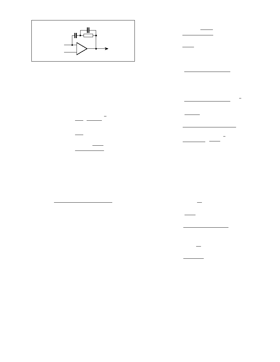
Fig. 8 Third order loop filter circuit diagram
Loop Filter Design
Generally, the third order filter configuration shown in Fig. 8
gives better results than the more commonly used second order
because the reference sidebands are reduced. Three equations
are required to determine values for the three constants, where
The equations are:
t
1
=
C
1
R
1
t
2
=
R
2
(
C
1
1
C
2
)
t
3
=
C
2
R
2
...(2)
...(3)
...(1)
t
2
=
1
v
n
2
t
3
2
2
tan F
0
1
t
3
=
v
n
t
1
=
K
f
K
0
v
n
2
N
11
v
n
2
t
2
2
11
v
n
2
t
3
2
1
2
1
cos
F
0
where
K
f
is the phase detector gain factor in mA/radian
K
0
is the VCO gain factor in radians/seconds/V
N
is the division ratio from VCO to reference frequency
v
n
is the natural loop frequency
F
0
is the phase margin, normally set to 45
∞
Since the phase detector used is linear over a range of 2
p
radians, the phase detector gain is given by:
These values can now be substituted in equation (1) to obtain
a value for
C
1
and in equations (2) and (3) to determine values
for
C
2
and
R
2
.
Example
Calculate values for a loop with the following parameters:
Frequency to be synthesised
1000MHz
Reference frequency
10MHz
Division ratio
1000MHz/100MHz = 100
K
0
VCO gain factor
2
p3
10MHz/V
F
0
phase margin
45
∞
Phase comparator current
6∑3mA
The phase detector gain factor
K
f
= 6∑3/2p = 1mA/radian
mA/radian
Phase comparator current setting
2
p
K
f
=
From equation (3):
2
tan
45
∞
1
t
3
=
100kHz
3
2
p
1
cos 45
∞
t
3
= 659
3
10
2
9
=
628319
0∑4142
t
2
=
(100kHz
3
2
p
)
2
3
659
3
10
2
9
1
t
2
= 3∑844
3
10
2
6
Using these values in equation (1):
t
1
=
100
3
(100kHz
3
2
p
)
2
1
3
10
2
3
3
2
p3
10MHz/V
3
[A]
11
v
n
2
t
2
2
11
v
n
2
t
3
2
where A =
=
1
2
1
1
(100kHz
3
2
p
)
2
3
(3∑844
3
10
2
6
)
2
1
1
(100kHz
3
2
p
)
2
3
(659
3
10
2
9
)
2
t
1
=
t
1
= 3∑84
3
10
2
9
From equation (2):
= 1∑59
3
10
2
9
3
2∑415
39∑48
3
10
2
12
62832
6∑833
1∑1714
1
2
Substituting for C2:
3∑844
3
10
2
6
2
659
3
10
2
9
t
2
=
R
2
C
1
1
t
3
R
2
=
0∑0153
3
10
2
6
R
2
= 829∑4
=
659
3
10
2
9
829∑4
t
3
=
C
2
R
2
=
t
3
R
2
C
2
= 0∑794nF
Now,
t
1
=
C
1
C
1
= 3∑84nF
t
2
=
R
2
(
C
1
1
C
2
)
t
2
=
C
2
R
2
t
2
2
t
3
C
1
or,
R
2
=

M Mitel (design) and ST-BUS are registered trademarks of MITEL Corporation
Mitel Semiconductor is an ISO 9001 Registered Company
Copyright 1999 MITEL Corporation
All Rights Reserved
Printed in CANADA
TECHNICAL DOCUMENTATION - NOT FOR RESALE
World Headquarters - Canada
Tel: +1 (613) 592 2122
Fax: +1 (613) 592 6909
North America
Asia/Pacific
Europe, Middle East,
Tel: +1 (770) 486 0194
Tel: +65 333 6193
and Africa (EMEA)
Fax: +1 (770) 631 8213
Fax: +65 333 6192
Tel: +44 (0) 1793 518528
Fax: +44 (0) 1793 518581
http://www.mitelsemi.com
Information relating to products and services furnished herein by Mitel Corporation or its subsidiaries (collectively "Mitel") is believed to be reliable. However, Mitel assumes no
liability for errors that may appear in this publication, or for liability otherwise arising from the application or use of any such information, product or service or for any infringement of
patents or other intellectual property rights owned by third parties which may result from such application or use. Neither the supply of such information or purchase of product or
service conveys any license, either express or implied, under patents or other intellectual property rights owned by Mitel or licensed from third parties by Mitel, whatsoever.
Purchasers of products are also hereby notified that the use of product in certain ways or in combination with Mitel, or non-Mitel furnished goods or services may infringe patents or
other intellectual property rights owned by Mitel.
This publication is issued to provide information only and (unless agreed by Mitel in writing) may not be used, applied or reproduced for any purpose nor form part of any order or
contract nor to be regarded as a representation relating to the products or services concerned. The products, their specifications, services and other information appearing in this
publication are subject to change by Mitel without notice. No warranty or guarantee express or implied is made regarding the capability, performance or suitability of any product or
service. Information concerning possible methods of use is provided as a guide only and does not constitute any guarantee that such methods of use will be satisfactory in a specific
piece of equipment. It is the user's responsibility to fully determine the performance and suitability of any equipment using such information and to ensure that any publication or
data used is up to date and has not been superseded. Manufacturing does not necessarily include testing of all functions or parameters. These products are not suitable for use in
any medical products whose failure to perform may result in significant injury or death to the user. All products and materials are sold and services provided subject to Mitel's
conditions of sale which are available on request.