 | –≠–ª–µ–∫—Ç—Ä–æ–Ω–Ω—ã–π –∫–æ–º–ø–æ–Ω–µ–Ω—Ç: VP310 | –°–∫–∞—á–∞—Ç—å:  PDF PDF  ZIP ZIP |

VP310
Satellite Channel Decoder
Preliminary Information
SHORTFORM TECHNICAL MANUAL
DS5155 -1.00 21/04/99
Ordering Information
VP310 - Key Features
VP310 CG GQ1R
∑
Conforms to EBU specification for DVB-S and DirecTV specification for DSS.
∑
On-chip digital filtering supports 1 to 45MBaud Symbol rates.
∑
On-chip 6-bit 60 or 90MHz dual-ADC.
∑
High speed scanning mode for blind symbol rate and code rate acquisition.
∑
Up to ± 15MHz LNB frequency tracking.
∑
Fully digital timing and phase recovery loops.
∑
High level software interface for minimum development time.
∑
DiSEqCTM v1.1: control outputs for full control of LNB and dish.
Applications
∑
DVB 1 to 45MBaud compliant satellite receivers.
∑
DSS 20MBaud compliant satellite receivers.
∑
SCPC receivers. (Single Channel Per Carrier)
∑
SMATV trans-modulators. (Single Master Antenna TV)
∑
LMDS. (Local Multipoint Distribution Service)
∑
Satellite PC applications.
The VP310 is a QPSK/BPSK 1 to 45MBaud demodulator and channel decoder for
digital satellite television transmissions to the European Broadcast Union ETS 300 421
specification. It receives analog I and Q signals from the tuner, digitises and digitally
demodulates this signal, and implements the complete DVB/DSS FEC (Forward Error
Correction), and de-scrambling function. The output is in the form of MPEG2 or DSS
transport stream data packets. The VP310 also provides automatic gain control to the
RF front-end devices.
The VP310 has a serial I≤C port interface to the control microprocessor. Minimal
software is required to control the VP310 because of the built in automatic search and
decode control functions.

VP310 PRELIMINARY
DATA
2
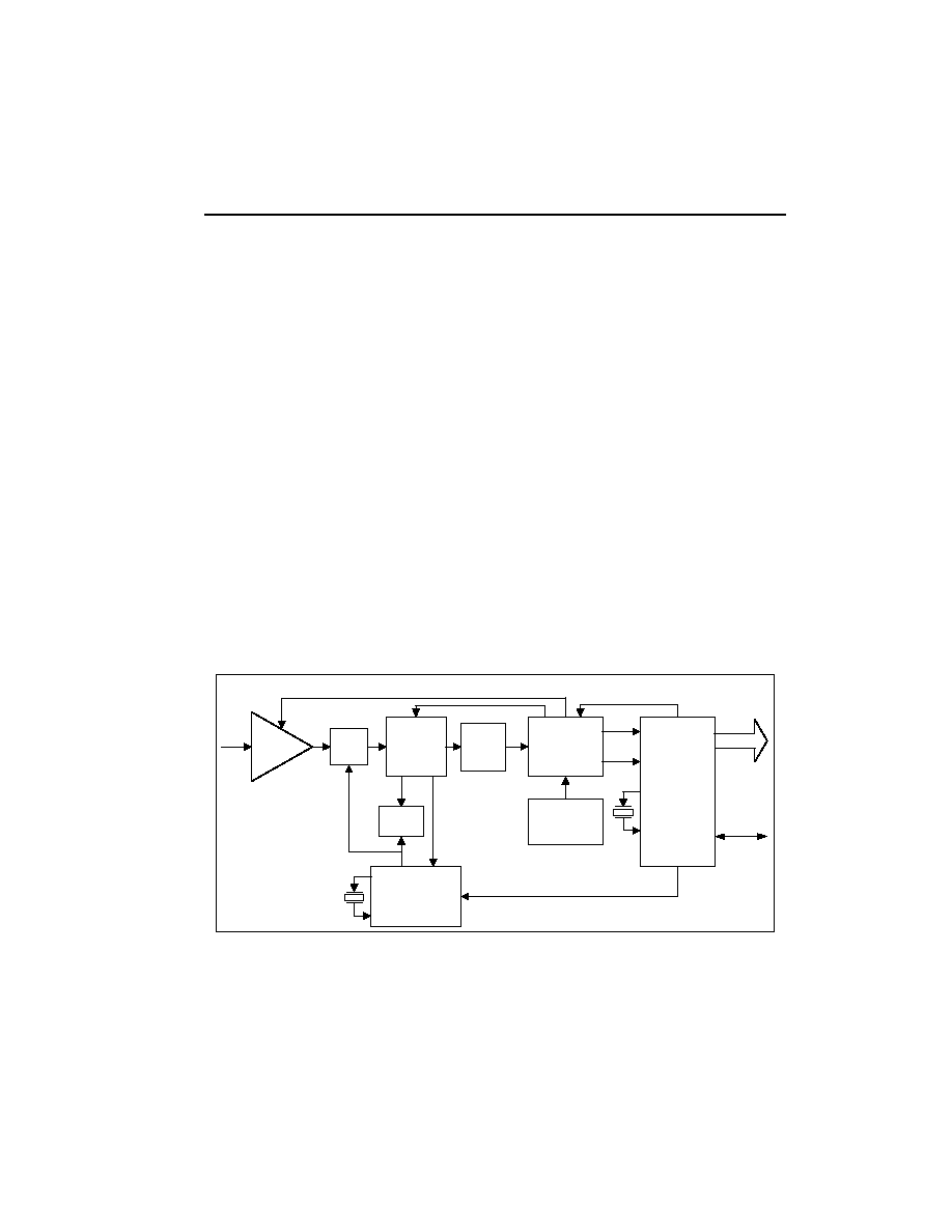
Overview
The VP310 is a QPSK/BPSK 1 to 45MBaud demodulator and channel decoder
for digital satellite television transmissions compliant to both DVB-S and DSS
standards and other systems, such as LMDS, that use the same architecture.
A Command Driven Control (CDC) system is provided making the VP310 very
simple to program. After the tuner has been programmed to the required
frequency, to acquire a DVB transmission, the VP310 requires a minimum of
five registers to be written, see Figure 15 on page 19. Activity flow diagrams for
initialisation and basic channel change are included in section 2.
The VP310 provides a monitor of Bit Error Rate after the QPSK module and
also after the Viterbi module.
For receiver installation, a high speed scan or `blind search' mode is available.
This allows all signals from a given satellite to be evaluated for frequency,
symbol rate and convolutional
coding scheme.
Dual ADC
Timing recovery
Matched filter
Phase recovery
I≤C
Interface
D V B
D S S
F E C
Analog
A G C
control
Acquisition
Control
Clock Generation
M P E G /
D S S
Packets
Bus I/O
Q I/P
I I/P
De-rotator
Decimation
Filteriing
Figure 1. VP310 Functional Block Diagram.

VP310 PRELIMINARY
DATA
3
Additional Features
∑
I≤C bus microprocessor interface.
∑
All digital clock and carrier recovery.
∑
On-chip PLL clock generation using low cost 10 to 15MHz crystal.
∑
3.3V operation.
∑
80 pin MQFP package.
∑
Low external component count.
∑
Commercial temperature range 0 to 70∞C.
Demodulator
∑
BPSK or QPSK programmable.
∑
Optional fast acquisition mode for low symbol rates.
Viterbi
∑
Programmable decoder rates 1/2, 2/3, 3/4, 5/6, 6/7, 7/8.
∑
Constraint length k=7.
∑
Trace back depth 128.
∑
Extensive SNR and BER monitors.
De-Interleaver
∑
Compliant with DVB and DSS standards.
Reed Solomon
∑
(204, 188) for DVB and (146,130) for DSS.
∑
Reed Solomon Bit-error-rate monitor to indicate Viterbi performance.
De-Scrambler
∑
EBU specification De-scrambler for DVB mode.
Outputs
∑
MPEG transport parallel & serial output.
∑
Integrated MPEG2 TEI bit processing for DVB only.
Application Support
∑
Channel decoder system evaluation board.
∑
I≤C interface board to PC.
∑
Windows based evaluation software.
∑
ANSI C generic software.
∑
Application support help desk via email/telephone.

VP310 PRELIMINARY
DATA
4
PLEASE NOTE: This manual has the following convention:
All numerical values are shown as decimal numbers, unless otherwise defined.
1. FUNCTIONAL DESCRIPTION
1.1 Introduction
VP310 is a single-chip variable rate digital QPSK/BPSK satellite demodulator and channel
decoder. The VP310 accepts base-band in-phase and quadrature analog signals and delivers an
MPEG or DSS packet data stream. Digital filtering in VP310 removes the need for any external
anti-alias filtering for all symbol rates from 1 to 45Mbaud. Frequency, timing and carrier phase
recovery are all digital and the only feed-back to the analog front-end is for automatic gain
control. The digital phase recovery loop enables very fine bandwidth control that is needed to
overcome performance degradation due to phase and thermal noise.
All acquisition algorithms are built into the VP310 controller. The VP310 can be operated in a
Command Driven Control (CDC) mode by specifying the Symbol rate and Viterbi code rate.
There is also a provision for a search for unknown Symbol rates and Viterbi code rates.
1.2 Analog-to-Digital Converter
The VP310 contains dual 6-bit A/D converters which each sample a 1.0Vpp single-ended analog
input at up to 90MHz. The fixed rate sampling clock is provided on-chip using a programmable
PLL needing only a low cost 10 to 15MHz crystal. Different crystal frequencies can be combined
with different PLL ratios, depending on the maximum symbol rate, allowing a flexible approach to
clock generation.
1.3 QPSK Demodulator
The demodulator in the VP310 consists of signal amplitude offset compensation, frequency offset
compensation, decimation filtering, carrier recovery, symbol recovery and matched filtering.
The decimation filters give continuous operation from 2Mbits/s to 90Mbits/s allowing one receiver
to cover the needs of the consumer market as well as the single carrier per channel (SCPC)
market with the same components without compromising performance, that is, the channel
reception is within 0.5dB from theory. For a given Symbol rate, control algorithms on the chip
detect the number of decimation stages needed and switch them in automatically.
The frequency offset compensation circuitry is capable of tracking out up to ± 15MHz frequency
offset. This allows the system to cope with relatively large frequency uncertainties introduced by
the Low Noise Block (LNB). Full control of the LNB is provided by the DiSEqC outputs from the
VP310. Horizontal / Vertical polarisation and an instruction modulated 22kHz signal are available
under register control. All DiSEqC v1.1 functions are implemented on the VP310.

VP310 PRELIMINARY
DATA
5
An internal state machine that handles all the demodulator functions controls the signal tracking
and acquisition. Various pre-set modes are available as well as blind acquisition where the
receiver has no prior knowledge of the received signal. Fast acquisition algorithms have been
provided for low Symbol rate applications. Full interactive control of the acquisition function is
possible for debug purposes.
In the event of a signal fade or a cycle slip, QPSK demodulator allows sufficient time for the FEC
to re-acquire lock, for example, via a phase rotation in the Viterbi decoder. This is to minimise the
loss of signal due to the signal fade. Only if the FEC fails to re-acquire lock for a long period
(which is programmable) would QPSK try to re-acquire the signal.
The matched filter is a root-raised-cosine filter with either 0.20 or 0.35 roll-off, compliant with
DSS and DVB standards. Although not a part of the DVB standard, VP310 allows a roll-off of
0.20 to be used with other DVB parameters.
An AGC signal is provided to control the signal levels in the tuner section of the receiver and
ensure the signal level fed to the VP310 is set at an optimal value under all reception conditions.
The VP310 provides comprehensive information on the input signal and the state of the various
parts of the device. This information includes Signal to Noise Ratio (SNR), signal level, AGC
lock, timing and carrier lock signals. A maskable interrupt output is available to inform the host
controller when events occur.
1.4 Forward Error Correction
The VP310 contains FEC blocks to enable error correction for DVB-S and DSS transmissions.
The Viterbi decoder block can decode the convolutional code with
rates 1/2, 2/3, 3/4, 5/6, 6/7 or
7/8. The block features automatic synchronisation and automatic code rate detection. The trace
back depth of 128 provides better performance at high code rates and the built-in synchronisation
algorithm allows the Viterbi decoder to lock onto signals with very poor signal-to-noise ratios.
Viterbi bit error rate monitor provides an indication of the error rate at QPSK output.
The 24-bit error count register in the Viterbi decoder allows the bit error rate at the output of the
QPSK demodulator to be monitored. The 24-bit bit error count register in the Reed-Solomon
decoder allows the Viterbi output bit error rate to be monitored. The 16-bit uncorrectable packet
counter yields information about the output packet error rate. These three monitors and the
QPSK SNR register allows the performance of the device and its individual components, such as
the QPSK demodulator and the Viterbi decoder, to be monitored extensively by the external
microprocessor.
The frame/byte align block features a sophisticated synchronisation algorithm to ensure reliable
recovery of DVB and DSS framed data streams under worst case signal conditions. The de-
interleaver uses on-chip RAM and is compatible with the DVB and DSS algorithms.
The Reed-Solomon decoder is a truncated version of the (255, 239) code. The code block size is
204 for DVB and 146 for DSS. The decoder provides a count of the number of uncorrectable
blocks as well as the number of bit errors corrected. The latter gives an indication of the bit error
rate at the output of the Viterbi decoder
.

VP310 PRELIMINARY
DATA
6
In DVB mode, spectrum de-scrambling is performed compatible with the DVB specification. The
final output is a parallel or serial transport data stream; packet sync; data clock; and a block error
signal. The data clock may be inverted under software control.
1.4.1.1 Viterbi error count measurement
A method of estimating the bit error rate at the output of the QPSK block has been provided in
the Viterbi decoder. The incoming data bit stream is delayed and compared with the re-encoded
and punctured version of
the decoded bit stream to obtain a count of errors see Figure 2 below.
VITERBI
DECODER
DELAY
COMP
ERROR COUNT
DATA BIT STREAM
VITERBI
ENCODER
Figure 2. Viterbi block diagram.
The measurement system has a programmable register to determine the number of data bits (the
error count period) over which the count is being recorded. A read register indicates the error
count result and an interrupt can be generated to inform the host microprocessor that a new
count is available.
The VIT_ERRPER H-M-L group of three registers is programmed with required number of data
bits (the error count period) (VIT_ERRPER[23:0]). The actual value is four times
VIT_ERRPER[23:0]. The count of errors found during this period is loaded by the VP310 into the
VIT_ERRCNT H-M-L trio of registers when the bit count VIT_ERRPER[23:0] is reached. At the
same time an interrupt is generated on the IRQ line. Setting the IE_FEC[2] bit in the IE_FEC
register enables the interrupt. Reading the register does not clear VIT_ERRCNT [23:0], it is only
loaded with the error count.
VP310 PRELIMINARY
DATA
7
VIT_ERRPER[23:0]
DATA BITS
ERROR
COUNT
VIT_ERRCNT[23:0]
0
0
IRQ
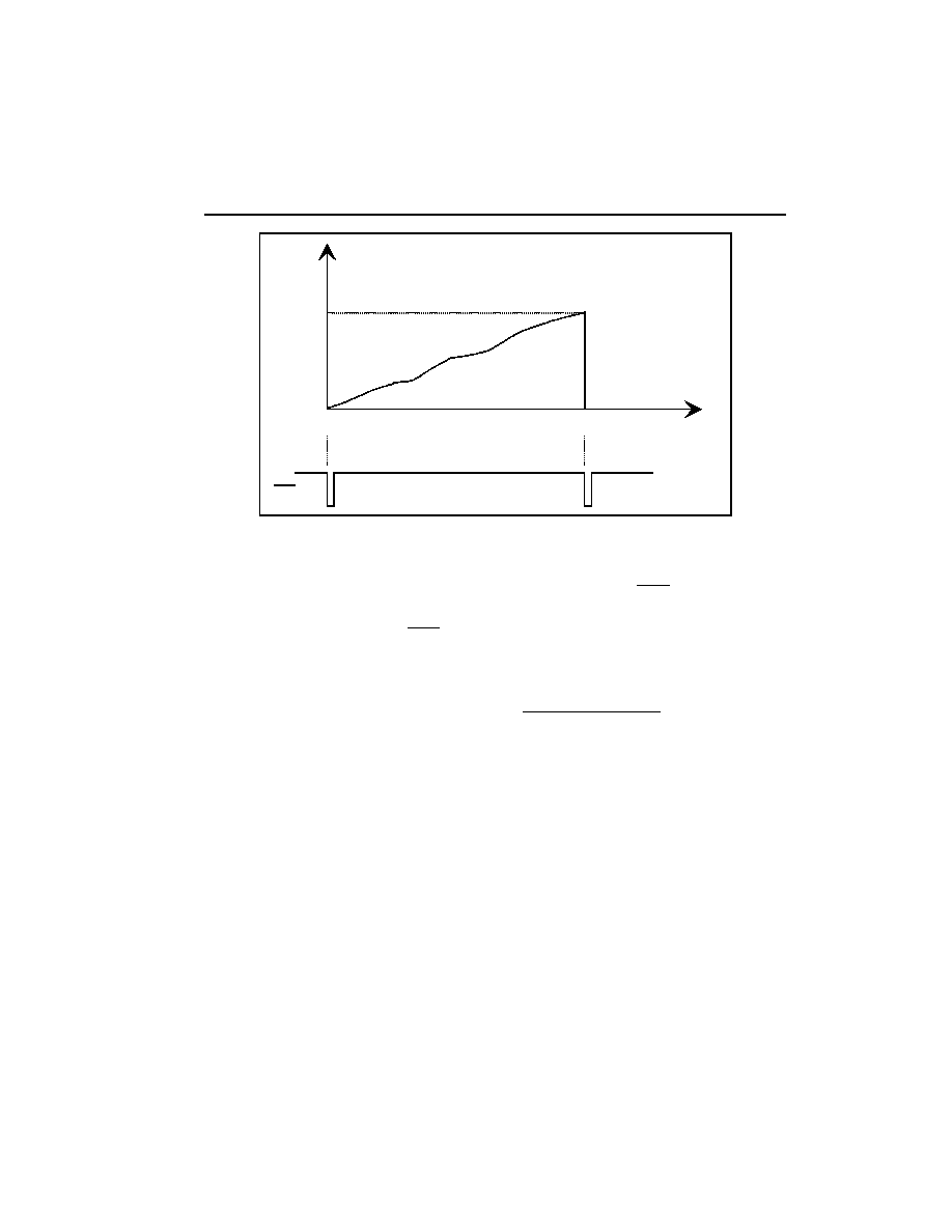
Figure 3. Viterbi error count measurement.
Figure 3 above shows the bit errors rising until the maximum programmed value of
VIT_ERRPER[23:0] is reached, when an interrupt is generated on the IRQ line to advise the
host microprocessor that a new value of bit error count has been loaded into the
VIT_ERRCNT[23:0] register. The IRQ line will go high when the IE_FEC register is read by the
host microprocessor.
VIT_ERRCNT[23:0] VIT_ERRPER[23:0]
The error count may be expressed as a ratio:
VIT_ERRCNT[23:0]
VIT_ERRPER[23:0] * 4
1.4.1.2 Viterbi error count coarse indication
To assist in the process of aligning the receiver dish aerial, a coarse indication of the number of
bit errors being received can be provided by monitoring the STATUS line with the following set up
conditions.
The frequency of the output waveform will be a function of the bit error count (triggering the
maximum value programmed into the VIT_MAXERR[7:0] register and the dish alignment on the
satellite. This VIT_MAXERR mode is enabled by setting the FEC_STAT_EN register bit B0.
Figure 4
on page
8
shows the bit errors rising to the maximum value programmed and triggering
a change of state on the STATUS line.
The output signal will be in the audio frequency range.

VP310 PRELIMINARY
DATA
8
S T A T U S
V I T E R B I
C O U R S E
B I T
E R R O R
C O U N T
V I T _ M A X E R R [ 7 : 0 ]
0
0
D A T A B I T S
Figure 4. Viterbi error count coarse indication.
1.4.2 The Frame Alignment block
The frame alignment algorithm detects a sequence of correctly spaced synchronising bytes in the
Viterbi decoded bit-stream and arranges the input into blocks of data bytes. Each
block consists
of 204 bytes for DVB and 147 bytes for DSS. In the DSS mode, the synchronising byte is
removed from the data stream, so only 146 bytes of a block are passed to the next stage. The
frame alignment block also removes the 180∞ phase ambiguity not removed by Viterbi decoder.
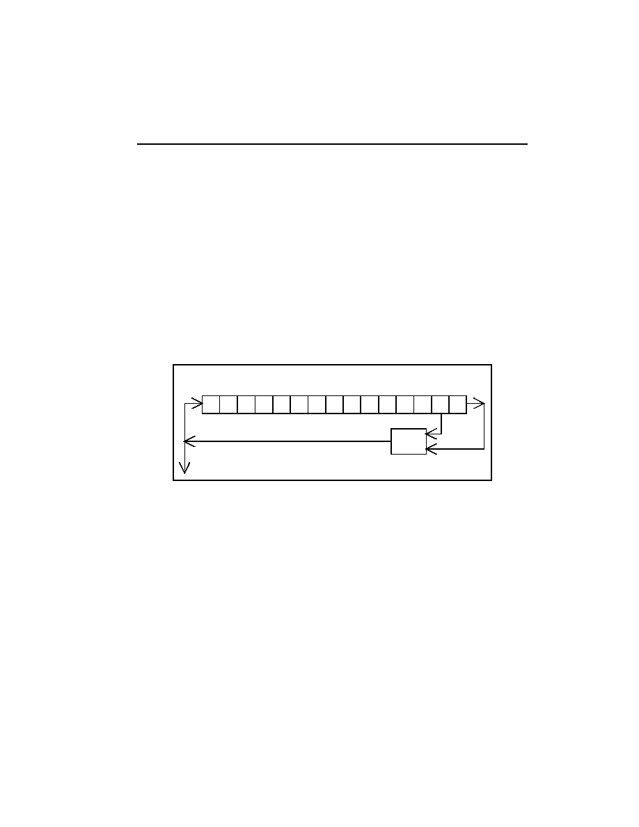
1.4.3 The De-interleaver block
1.4.3.1 DVB
Before transmission, the data bytes are interleaved with each other in a cyclic pattern of twelve.
This ensures the bytes are spaced out
to avoid the possibility of a noise spike corrupting a group
of consecutive message bytes. The diagram below shows conceptually how the convolutional de-
interleaving system works. The synchronisation byte is always loaded into the First-In-First-Out
(FIFO) memory in branch 0. The switch is operated at regular byte intervals to insert successively
received bytes into successive branches. After 12 bytes have been received, byte 13 is written
next to the synchronisation byte in branch 0, etc. In the VP310, this de-interleaving function is
realised using on-chip Random Access Memory (RAM).
VP310 PRELIMINARY
DATA
9
0
1
2
3
4
5
6
7
8
9
10
11
0
1
2
3
4
5
6
7
8
9
10
11
Sync word route
17x1
17x2 bytes
17x3 bytes
17x4 bytes
17x5 bytes
17x6 bytes
17x7 bytes
17x8 bytes
17x9 bytes
17x10 bytes
17x11 bytes
one
byte per
position
Figure 5. DVB Conceptual diagram
of the convolutional de-interleaver block
.
1.4.3.2 DSS
Before transmission, the data bytes are interleaved with each other in a cyclic pattern of thirteen.
This ensures the bytes are spaced out to avoid the possibility of a noise spike corrupting a group
of consecutive message bytes. The diagram below shows conceptually how the convolutional de-
interleaving system works. On the VP310, this function is realised in the same Random Access
Memory (RAM) as used for DVB, but utilising different addressing algorithm.
1 2 D
1 2 D
1 2 D
0
1
O u t p u t
1 4 5
Input
2
Figure 6. DSS Conceptual diagram of the convolutional de-interleaver block.

VP310 PRELIMINARY
DATA
10
1.4.4 The Reed Solomon Decoder
block
DVB and DSS data are encoded using shortened versions of the Reed-Solomon code of block
length 255, containing 239 message bytes and 16 check bytes, that is (255,239) with T = 8. Both
encoders use the same generator polynomial. The code block size for DVB is 204 and that for
DSS is 146. Hence DVB code is (204, 188) and DSS code is (146, 130), with both having T = 8.
The block structure of the DVB and DSS Reed-Solomon codes are as shown in Figure 7 and
Figure 8 on page 10.
The Reed-Solomon decoder can correct up to eight byte errors per packet. If there are more than
8 bytes containing errors, the packet is flagged as uncorrectable using the pin BKERR. In the
case of DVB the transport error indicator (TEI) bit of the MPEG packet is set to 1, if setting of TEI
is enabled.
S y n c b y t e
187 bytes
S y n c b y t e
187 bytes
16 check bytes
R e e d S o l o m o n e n c o d e d b l o c k
M P E G t r a n s p o r t p a c k e t
Figure 7. DVB block structure.
130 bytes
130 bytes
16 check bytes
R e e d S o l o m o n e n c o d e d b l o c k
DSS transport packet
Figure 8. DSS block structure.
VP310 PRELIMINARY
DATA
11
1.4.5 The Energy Dispersal (de-scrambler) block, DVB only
Before Reed Solomon encoding in the DVB transmission system, the MPEG2 data stream is
randomised using the configuration shown in Figure 9 below. This is a Pseudo Random Binary
Sequence (PRBS) generator, with the polynomial:
1 + X
14
+ X
15
The PRBS registers are loaded with the initialisation sequence as shown, at the start of the first
transport packet in a group of eight packets. This point is indicated by the inverted sync byte
B8
hex
. The normal DVB sync byte is 47
hex
. The data starting with the first byte after the sync byte
is randomised
by exclusive-ORing data bits with the PRBS.
(The sync bytes themselves are not
randomised).
In the decoder, the process of de-randomising or de-scrambling the data is exactly the same as
described above. The de-scrambler also inverts the sync byte B8hex so that all MPEG output
packets have the same synch byte 47hex.
1
2
3
4
5
6
7
8
9
10
11
12 13
14
15
1
0
0
1
0
1
0
1
0
0
0
0
0
0
0
Initialisation sequence
XOR
Figure 9. DVB Energy dispersal conceptual diagram.
1.4.6 Output stage
Transport stream can be output in a byte-serial or bit-serial mode. The output interface consists
of an 8-bit output, output clock, a packet validation level, a packet start pulse and a block error
indicator.
The output clock rate depends on the Symbol rate, QPSK/BPSK choice, convolutional (Viterbi)
coding rate, DVB/DSS choice and byte-parallel or bit-serial output mode. This rate is computed
by VP310 to be very close to the minimum required to output packet data without packet overlap.
Furthermore, the packets at the output of VP310 are as evenly spaced as possible to minimise
packet position movement in the transport layer. The maximum movement in the packet
synchronisation byte position is limited to
±
one output clock period.

VP310 PRELIMINARY
DATA
12
1.5 Control
Automatic Symbol Rate Search, Code Rate Search, Signal Acquisition and Signal Tracking
algorithms are built into the VP310 using a sophisticated on-chip controller. The software
interaction with the device is via a simple Command Driven Control (CDC) interface. This CDC
maps high level inputs such as symbol rates in MBaud and frequencies in MHz, to low level on-
chip register settings. The on-chip control state machine and the CDC significantly reduces the
software overhead as well as the channel search times. There is also an option for the host
processor to by-pass both the CDC as well as the on-chip controller and take direct control of the
QPSK demodulator.
Command
Driven
Control
High level input/output
(MBaud, MHz)
VP310
format
registers
Acquistion/
Track
State machine
Q P S K
Low level register read/write
Figure 10. VP310 Control Structure.
Once the VP310 has locked up, any frequency offset can be read from the LNB_FREQ error
registers 7 and 8. The frequency synthesiser under the software control can be re-tuned in
frequency to optimise the received signal within the SAW bandwidth. Note that VP310
compensates for any frequency offsets before QPSK demodulation. Hence a frequency offset will
not necessarily lead to a performance loss. Performance loss will occur only if part of the signal
is cut off by the SAW or base-band filter, due to this frequency offset. This will happen only if the
symbol rate is close to maximum supported by that filter. In such an event it is recommended
that front-end be re-tuned to neutralise this error before the SAW filter. It is then necessary for the
VP310 to re-acquire the signal.
The VP310 can generate control signals to enable full control of the dish and LNB. The chip
implements the signals needed for the full DiSEqC v1.1 specification. This includes high/low
band selection, polarisation and dish position.
The microprocessor interface is via the primary I≤C bus. The tuner control from the VP310 is via
either I≤C bus or 3-wire bus, recreated on the General Purpose Port (GPP).
1.5.1 Known Symbol Rate and Code Rate mode
In this mode, the Symbol rate in MBaud and Viterbi code rate are the only values needed to start
the VP310 searching for the signal. The CDC module maps the high level parameters into the
various low level register settings needed to acquire and track the signal. The low level registers
may be read and directly modified to suit very specific requirements. However, this is not
recommended.
VP310 PRELIMINARY
DATA
13
1.5.2 Symbol Rate and Code Rate Search mode
Where the Symbol rate and/or the Viterbi code rate are unknown, the VP310 can be programmed
to search for QPSK/BPSK signals. The user should define the range(s) over which the search is
required. The VP310 will then locate and track any signal detected. Failure to find a QPSK signal
specified frequency and specified symbol rate ranges will be indicated by interrupts. VP310 will
carry on searching these ranges after issuing these interrupts. When the VP310 has locked onto
a signal, the Symbol rate in MBaud may be read from the MONITOR registers. The Viterbi code
rate may be read from the FEC_STATUS register. This search facility is primarily for the initial
installation of a set top box.
1.6 Applications Information
1.6.1 IF conversion
The VP310 has been designed for maximum flexibility in the satellite application and many
options are available. The diagram shown below employs a single conversion system with an IF
of 480MHz. The SAW filter is selected for the maximum data rate expected and a SAW resonator
is used with the I/Q down converter to mix the input down to baseband I and Q channels for the
VP310 to digitise. The fixed sampling frequency of the VP310 is selected to be either 90MHz or
60 MHz depending on the maximum Symbol rate the application must work with. The sample
rate must be greater than or equal to twice the Symbol rate. For a table showing SAW bandwidth
versus Symbol rate.
Tuner
S L 2 0 1 7
I/Q Down-
converter
S L 1 7 2 0
Channel
Decoder
V P 3 1 0
Synthesiser
S P 5 7 6 9
S A W
Resonator
S A W
filter
I≤C bus control
AGC control
T r a n s p o r t
stream O/P
I≤C control
I I/P
Q I/P
RF I/P
AGC control
Tank
A G C
A M P
I/P
filter
Figure 11. Single Conversion System Diagram.

VP310 PRELIMINARY
DATA
14
1.6.2 Direct conversion
Figure 12 below shows a direct conversion system that mixes the L-band input to the tuner
directly down to I and Q baseband channels at zero intermediate frequency.
The RF AGC amp and tracking filter provide the required tuner noise figure and limit the total
power reaching the SL1925. These elements also give isolation between the SL1925 local
oscillator and the L-band tuner input. This is an important factor since both signals are at the
same frequency.
The baseband filter is an anti-alias filter. This replaces the filtering normally carried out with a
SAW filter in conventional single conversion tuners.
It is important to note that all the channel filtering needed to isolate low Baud rate signals is
contained within the VP310. The low pass filter before VP310 is designed not to filter channels,
but to minimise any aliasing due to sampling. To illustrate this, let the sampling frequency be 90
MHz and the maximum symbol rate be 45 MBaud. The bandwidth of the 45 MBaud QPSK signal,
with 0.35 roll-off, is about 60 MHz. If the channel has been mapped precisely to base-band, the
pass-band of the low pass filter should extend up to 30 MHz. However, it is preferable to make
this bandwidth larger by about 5 MHz, partly to reduce the in-band phase distortion introduced by
the filter and partly to reduce the loss of signal due to LNB offset. The filter must attenuate
signals beyond 60 MHz by about 30 dB, as these signal will alias to the useful frequency range
with 90 MHz sampling.
Although the system is designed for 45 MBaud, if the actual symbol rate is much lower, say 1
MBaud, then VP310 will automatically introduce all the digital filtering needed to isolate the 1
MBaud signal.
Direct
Conversion
Tuner
S L 1 9 2 5
Low pass
Filter
Channel
Decoder
V P 3 1 0
Synthesiser
SP5655/
S P 5 7 6 9
I≤C bus control
T r a n s p o r t
stream O/P
I≤C control
I I/P
Q I/P
RF I/P
AGC control
Tank
A G C
A M P
S L 1 9 1 4
I
Q
Figure 12. Direct Conversion System Diagram.

VP310 PRELIMINARY
DATA
15
2. VP310 software control
This section describes the sequences of register operations needed to acquire DVB and DSS
channels with known or unknown parameters.
Communication with the VP310 is via a standard I≤C bus and the first byte following the chip
address, in write mode, is the register address (RADD).
The register map is organised to group important Read registers at the lowest addresses, then
the main control Write registers in the next block of addresses.
The first register to be written must be the Configuration register, which has been placed at the
highest register address, because it is only written once during the initialisation sequence.
The CONFIG register can only be reset by the hardware reset. The VP310 is held in a power
saving mode following the hardware reset.
After a hardware reset, the VP310 must be taken out of the power save mode by writing a one to
the MSB of the CONFIG register. When VP310 is not being used it can be put back into the
power save mode by writing a zero to the MSB of CONFIG.
2.1 Initialisation sequence
VP310 will be in the power save mode after a hardware reset. The first command to be written
must be to the CONFIGURATION register at address 127. After loading this register, wait 150µs
before writing to the RESET register. During this wait, the tuner can programmed to the required
channel frequency via the General Purpose Port (register 20).
Next write 128 to the RESET register (21) to reset the VP310 state machine and all parameter
registers to the default settings.
The default settings of the VP310 assumes a Gain Control Amplifier with a negative gain Vs
voltage slope, i.e. the gain increases with decreasing voltage. However, if this slope is positive,
the polarity of the AGC control signal can be inverted by programming 1 to bit B0 of the
AGC_CTRL register, i.e. by changing the default AGC_CTRL setting from 38 to 39. It is best to
do this immediately after writing 128 to the RESET register. Then the AGC loop can settle whilst
the other registers of VP310 are programmed. Note that the initial value, minimum value and the
maximum value of the AGC control voltage can also be programmed using the corresponding
VP310 registers.
After this, the LNB controls are defined, in register (22) DISEQC_MODE.
The signal parameters should then be written to the VP310. The symbol rate (registers 23 & 25
SYM_RATE) may be specified within ±2% of the required value, absolute precision is not
required to achieve successful lock and tracking. If the symbol rate is unknown, a search mode is
available.

VP310 PRELIMINARY
DATA
16
Selecting the correct bit of register (25) VIT_MODE, if known, programs the convolutional code
rate. If the code rate is unknown, some or all of the bits of VIT_MODE may be set to force the
VP310 to search for the code rate.
Finally, the VP310 is given a GO command, register (27) GO = 1, to release the state machine
and to start the signal acquisition sequence. This is summarised as an example in the following
flow diagram.
VP310 PRELIMINARY
DATA
17
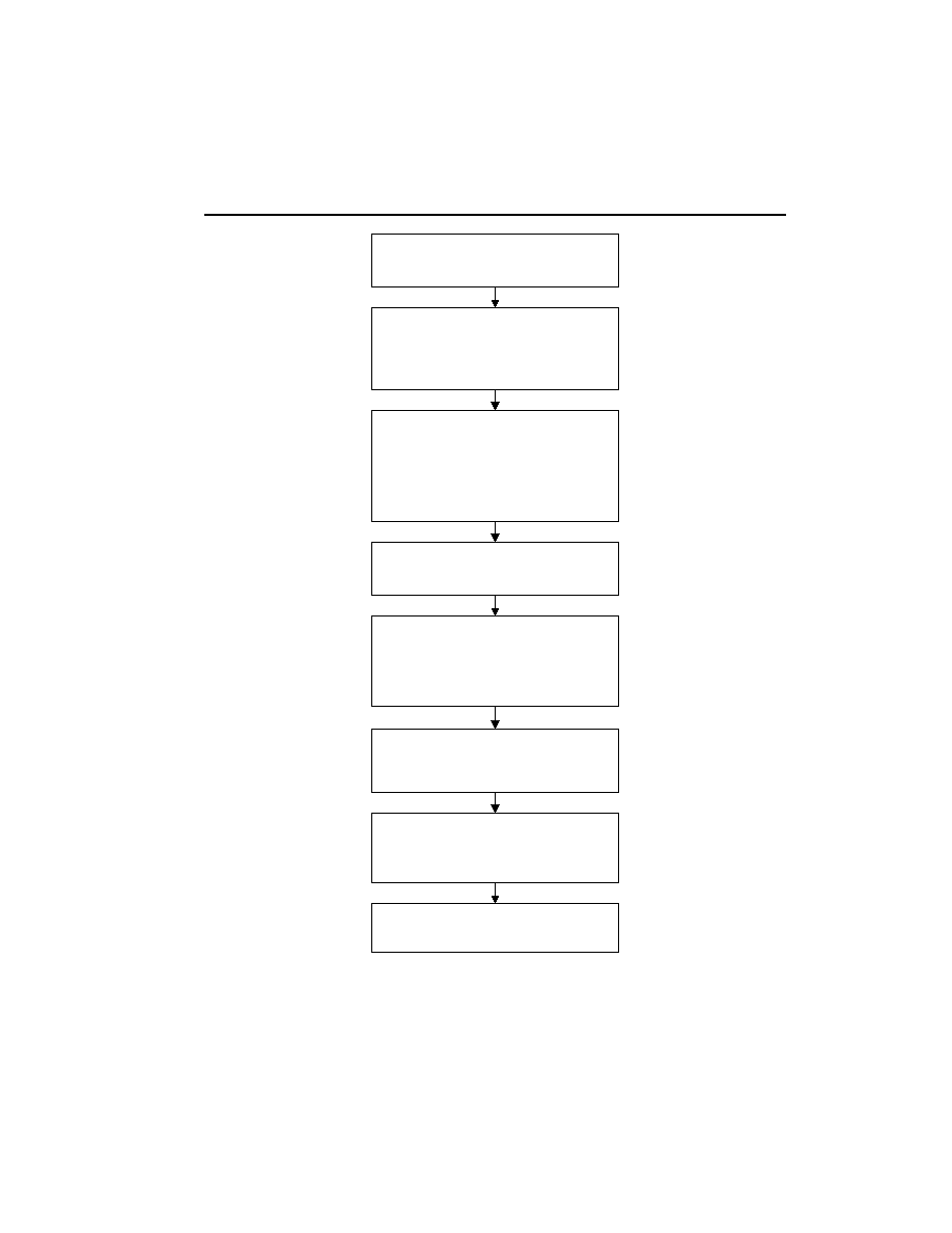
Enable VP310 : Program CONFIG
Reg 127 = 136 (88hex)
Program tuner via GPP in 'pass through mode'
open port with Reg 20 = 64 (40hex)
send TUNER DATA via I2C bus (5 bytes).
close port with Reg 20 = 0
Reset VP310 to default register settings
Reg 21 = 128 (80hex)
Set AGC_SL (if required)
Initialise registers: reg 49 = 50 (32hex);
reg 86 = 20 (14hex); reg 87 = 18 (12hex);
reg 88 = 2; reg 89 = 1; reg 90 = 0;
reg 91 = 0; reg 92 = 0; reg 93 = 0.
DiSEqC mode
eg Horizontal with 22kHz on:
Reg 22 = 65 (41hex)
Signal input - Symbol rate
eg 27.5 MBaud:
Reg 23 = 27 (1Bhex) DEFAULT state
Reg 24 = 128 (80hex) DEFAULT state
Viterbi code rate
eg V_IQ swap not set, CR = 3/4:
Reg 25 = 4 (4hex)
QPSK control
eg DVB : roll-off = 0.35:
Reg 26 = 0 DEFAULT state
GO
Release reset state to start signal capture
Reg 27 = 1
Figure 13. Initialisation sequence in DVB mode.

VP310 PRELIMINARY
DATA
18
2.2 Spectral Inversion
Spectral inversion of the QPSK signal can be caused by the transmitter or the receiver front-end.
In the latter case, this could happen due to the way I-Q conversion is carried out or because the I
and Q wires are swapped between the I-Q converter and the VP310. If spectral inversion is
caused by the receiver front-end, then this must be removed by swapping I and Q (within VP310)
before QPSK demodulation, by setting Q_IQ_SP bit B6 of QPSK_CTRL register (26) to 1.
If no spectral inversion is caused by the receiver front-end design, then bit B6 of QPSK_CTRL
must always be held at zero. If the transmitted signal is known to be spectrally inverted, then
V_IQ_SP bit B6 of the VIT_MODE register (25) must be set to 1. Then I and Q are swapped after
QPSK demodulation. If the spectral inversion status of the transmitted signal is not known, then
after QPSK has locked (i.e. QPSK_CT_LOCK = 1), the software must try to achieve FEC lock
with the bit B6 of VIT_MODE register first at zero and then at one.
2.3 Simple channel change sequence
If the VP310 is running, to change channel keeping the same signal conditions, it is only
necessary to change the tuner data and possibly the DiSEqC data. NO reset is necessary.
Program tuner via GPP in 'pass through mode'
open port with Reg 20 = 64 (40hex)
send TUNER DATA via I2C bus (5 bytes).
close port with Reg 20 = 0
DiSEqC mode
eg Vertical with 22kHz on:
Reg 22 = 1 (01hex)
G O
Re-acquire signal
Reg 27 = 1
Figure 14. Simple channel change sequence.

VP310 PRELIMINARY
DATA
19
2.4 Channel change sequence with a new symbol rate
If the VP310 is running, to change channel and Symbol rate but not Viterbi coding rate, change
the tuner data and possibly the DiSEqC data and Symbol rate. NO reset is necessary.
Program tuner via GPP in 'pass through mode'
open port with Reg 20 = 64 (40hex)
send TUNER DATA via I2C bus (5 bytes).
close port with Reg 20 = 0
DiSEqC mode
eg Horizontal with 22kHz on:
Reg 22 = 65 (41hex)
Signal input - Symbol rate
eg 22.0 MBaud :
Reg 23 = 22 (16hex)
Reg 24 = 0
Viterbi code rate
eg V_IQ swap not set, CR = 5/6:
Reg 25 = 8 (8hex)
GO
Re-acquire signal
Reg 27 = 1
Figure 15. Channel change sequence with new Symbol rate, DVB mode.

VP310 PRELIMINARY
DATA
20
2.5 Channel change sequence with Search mode
If the signal parameters are unknown, it is possible to instruct the VP310 to find a digital signal
and report the parameters found. Registers 24 and 25 are programmed with the expected
range(s) and the search mode bit SYM_RATE[B15] is set high. A code rate search is forced by
programming more than one bit in VIT_MODE (26) register.
Note: code rate 6/7 is not searched for DVB mode.
If a signal with the specified symbol rate range (or ranges) is not found in the frequency range
searched, a QPSK Baud End interrupt (Bit B6, QPSK_INT_L (2)) is issued.
Program tuner via GPP in 'pass through mode'
open port with Reg 20 = 64 (40hex)
send TUNER DATA via I2C bus (5 bytes).
close port with Reg 20 = 0
DiSEqC mode
eg Horizontal with 22kHz on:
Reg 22 = 65 (41hex)
Signal input - Search mode
eg for SYS_CLK=60MHz and
30 to 20 MBaud range:
Reg 23 = 136 (88hex)
Reg 24 = 0
Viterbi code rate search
eg V_IQ swap not set:
Reg 25 = 47 (2Fhex)
G O
Re-acquire signal
Reg 27 = 1
Figure 16. Channel change sequence with search mode, DVB mode.

VP310 PRELIMINARY
DATA
21
When the VP310 QPSK section has locked to the signal, this is indicated in register (6) by
QPSK_STAT H[B0] = 1. The symbol rate found can be read from registers (123 ≠ 124)
MONITOR, provided the register (103) MON_CTRL = 3. The tolerance of the result is ±0.25%.
The 14 MSBs of this result (discarding two LSBs) may be written as the 14 LSBs of the 16-bit
register pair (23 and 24) SYM_RATE in the non-search mode for re-acquisition of the same
channel.
The FEC is locked to the signal, when the Byte Align lock in FEC_STATUS[B2] = 1. Then the
code rate found can be read from FEC_STATUS[B6-4], see register 6 for details.
Program MONITOR to read Symbol rate
MON_CTRL Reg 103 = 3
Read Symbol rate from MONITOR registers 123 & 124.
Symbol rate = MONITOR_H/4 + MONITOR_L/1024 MBaud
eg if MONITOR_H = 27 and MONITOR_L = 136
then Symbol rate = 27.53125 MBaud
ie 27.5 MBaud ±0.25%
Read code rate from FEC_STATUS[B6-4] register 6.
eg if FEC_STATUS = 2C hex
signal is locked and the code rate = 3/4
Figure 17. Results of Symbol rate and code rate search, DVB or DSS mode.

VP310 PRELIMINARY
DATA
22
2.6 DSS mode of acquisition
This mode is very similar to the DVB mode, except that the Symbol rate is fixed at 20 MBaud.
Two code rates are used: DSS-A uses 2/3 or DSS-B uses 6/7. These are programmed in the
register (127) CONFIG. If the code rate is unknown, program both DSS-A and DSS-B to force the
VP310 to do a code rate search. After changing the CONFIG register, a delay of 150µs should be
enforced before programming the RESET register. The Tuner may be programmed via the GPP
during this delay period.
Since both symbol rate and code rate are defined by programming the CONFIG register, the
contents of registers (23-24) SYM_RATE and register (25) VIT_MODE are ignored in DSS mode.
Enable VP310 : Program CONFIG
e g D S S - A
Reg 127 = 166 (A8hex)
Program tuner via GPP in 'pass through mode'
open port with Reg 20 = 64 (40hex)
send TUNER DATA via I2C bus (5 bytes).
close port with Reg 20 = 0
Reset VP310 to default register settings
Reg 21 = 128 (80hex)
Set AGC_SL (if required)
Initialise registers: reg 25 = 16 (10hex);
reg 49 = 50 (32 hex) ; reg 50 = 20 (14hex);
reg 86 = 20 (14hex); reg 87 = 18 (12hex);
reg 88 = 2; reg 89 = 1; reg 90 = 0;
reg 91 = 0; reg 92 = 0; reg 93 = 0.
DiSEqC mode
eg Horizontal with 22kHz on:
Reg 22 = 65 (41hex)
G O
Re-acquire signal
Reg 27 = 1
Figure 18. Initialisation sequence in DSS mode.

VP310 PRELIMINARY
DATA
23
2.7 Signal and Performance Monitors
The LNB error frequency can be obtained from LNB_FREQ registers (7 ≠ 8). Any LNB error may
be removed by offsetting the LNB frequency and re-tuning the tuner by the indicated amount.
However, note that VP310 compensates for this frequency error before QPSK demodulation.
Hence it is not necessary to re-tune the front-end unless this LNB error causes a significant
amount of signal energy to be lost due to anti-alias filtering.
The tuner RF signal level indication can be obtained from AGC H and AGC M registers (108 ≠
109).
VP310 input signal level indication can be obtained from SIG_LEV register (19).
An indication of Signal to Noise Ratio (SNR) can be obtained from M_SNR registers (9 ≠ 10)
where a formula is given. This measurement is only intended as a guide to the SNR of the
channel being received. It should not be taken as the absolute value of SNR.
QPSK output Bit Error Rate is available by dividing the reading from VIT_ERRCNT registers (11
≠ 13) by the reading from VIT_ERRPER registers (83 ≠ 85).
Viterbi output Bit Error Rate is available by reading RS_BERCNT registers (14 ≠ 16). Two
readings are taken with a known time interval separating them. The first reading resets the
counter at the start of the time period, so it is ignored.
The Reed Solomon uncorrected block error count can be found from RS_UBC registers (17 ≠
18). This reading is related to the cycle slip performance of the tuner. The measurement
technique is similar to that for the Viterbi Bit Error Rate above, two readings being taken over a
defined time period. In this case the period will usually be very long, say 24 hours, to accumulate
a reasonable count.
VP310 PRELIMINARY
DATA
24
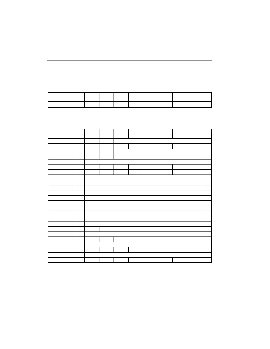
3. VP310 register map
RADD is a virtual register with no address containing the address of the register to be accessed.
It is written immediately after the I≤C write address.
NAME
ADR
B7
B6
B5
B4
B3
B2
B1
B0
DEF
hex
RADD
N/A
IAI
AD6
AD5
AD4
AD3
AD2
AD1
AD0
-
3.1 Write / Read register map
NAME
ADR
B7
B6
B5
B4
B3
B2
B1
B0
DEF
hex
GPP_CTRL
20
Reserved I2C_PAS
GPP_DIR[2:0]
GPP_PIN[2:0]
20
RESET
21
FR_310
PR_310
FR_QP
PR_QP
FR_VIT
PR_VIT
PR_BA
PR_DS
00
DISEQC_MODE
22
Reserved
HV
DISEQC instruction length
22kHz mode
00
SYM_RATE H
23
SEARCH Reserved
SYM_RATE[13:8] in MBaud (high byte)
1B
SYM_RATE L
24
SYM_RATE[7:0] in MBaud (low byte)
80
VIT_MODE
25
Reserved V_IQ_SP CR 7/8
CR 6/7
CR 5/6
CR 3/4
CR 2/3
CR 1/2
44
QPSK_CTRL
26
Reserved Q_IQ_SP Reserved Reserved Reserved AFC_M Reserved ROLL_20
00
GO
27
Reserved
GO
00
IE_QPSK H
28
IE_QPSK[23:16] Interrupt enable QPSK (high byte)
00
IE_QPSK M
29
IE_QPSK[15:8] Interrupt enable QPSK (middle byte)
00
IE_QPSK L
30
IE_QPSK [7:0] Interrupt enable QPSK (low byte)
00
IE_FEC
31
IE_FEC[7:0] Interrupt enable FEC
00
QPSK_STAT_EN
32
QPSK_STAT_EN[7:0] Enable various QPSK outputs on STATUS pin
00
FEC_STAT_EN
33
FEC_STAT_EN[3:0] Enable various FEC outputs on STATUS pin
04
SYS_CLK
34
SYS_CLK[7:0] - System clock frequency x2 in MHz
00
DISEQC_RATIO
35
DISEQC_RATIO[7:0]
00
DISEQC_INSTR
36
DISEQC Instruction [7:0]
00
FR_LIM
37
Reserved
FR_LIM[6:0] - Freq. Limit in MHz
30
FR_OFF
38
FR_OFF[7:0] - Freq. Offset in MHz
00
AGC_CTRL
39
Reserved Reserved
AGC_SD[1:0]
AGC_BW[2:0]
AGC_SL
26
AGC_REF
41
AGC_REF[7:0] AGC reference level
67
OP_CTRL
96
Reserved BKERIV MCLKIV EN_TEI
BSO
BA_LK[2:0]
33
MON_CTRL
103
MON_CTRL[7:0] Monitor control
00
CONFIG
127
310_EN
DSS_B
DSS_A
BPSK
PLL_FACTOR[1:0] CRYS15 ADCEXT
08

VP310 PRELIMINARY
DATA
25
3.2 Read only register map
Writing to these registers will have no effect.
NAME
ADR
B7
B6
B5
B4
B3
B2
B1
B0
DEF
hex
QPSK_INT H
00
QPSK_INT[23:16] Interrupt QPSK (high byte)
00
QPSK_INT M
01
QPSK_INT [15:8] Interrupt QPSK (middle byte)
00
QPSK_INT L
02
QPSK_INT [7:0] Interrupt QPSK (low byte)
00
FEC_INT
03
FEC_INT[7:0] Interrupt FEC
00
QPSK_STAT H
04
QPSK STATUS[15:8] (high byte)
00
QPSK_STAT L
05
QPSK STATUS[7:0] (low byte)
00
FEC_STATUS
06
FEC STATUS[7:0]
00
LNB_FREQ H
07
LNB_FREQ[15:8] Measured LNB frequency error (high byte)
00
LNB_FREQ L
08
LNB_FREQ [7:0] Measured LNB frequency error (low byte)
00
M_SNR H
09
Reserved
M_SNR[14:8] Measured SNR (high byte)
00
M_SNR L
10
M_SNR [7:0] Measured SNR (low byte)
00
VIT_ERRCNT H
11
VIT_ERRCNT[23:16] - Viterbi error count (high byte)
00
VIT_ERRCNT M
12
VIT_ERRCNT [15:8] - Viterbi error count (middle byte)
00
VIT_ERRCNT L
13
VIT_ERRCNT [7:0] - Viterbi error count (low byte)
00
RS_BERCNT H
14
RS_BERCNT [23:16] - Reed Solomon bit errors corrected (high byte)
00
RS_BERCNT M
15
RS_BERCNT[15:8] - Reed Solomon bit errors corrected (middle byte)
00
RS_BERCNT L
16
RS_BERCNT[7:0] - Reed Solomon bit errors corrected (low byte)
00
RS_UBC H
17
RS_UBC [15:8] - Reed Solomon uncorrected block errors (high byte)
00
RS_UBC L
18
RS_UBC[7:0] - Reed Solomon uncorrected block errors (low byte)
00
SIG_LEVEL
19
SIG_LEVEL[11:4] - Signal level at VP310 input
00
AGC H
108
AGC[23:16] - Front end AGC (high byte)
00
AGC M
109
AGC[15:8] - Front end AGC (middle byte)
00
AGC L
110
AGC[7:0] - Front end AGC (low byte)
00
FREQ_ERR1 H
111
FREQ_ERR1[23:16] Input frequency error course (high byte)
00
FREQ_ERR1 M
112
FREQ_ERR1[15:8] Input frequency error course (middle byte)
00
FREQ_ERR1 L
113
FREQ_ERR1[7:0] Input frequency error course (low byte)
00
FREQ_ERR2 H
114
FREQ_ERR2[15:8] Input frequency error fine (high byte)
00
FREQ_ERR2 L
115
FREQ_ERR2[7:0] Input frequency error fine (low byte)
00
SYM_RAT_OP H 116
SYM_RAT_OP[15:8] Symbol Rate Output (high byte)
00
SYM_RAT_OP L
117
SYM_RAT_OP [7:0] Symbol Rate Output (low byte)
00
MONITOR H
123
MONITOR[15:8] Monitor (high byte)
00
MONITOR L
124
MONITOR[7:0] Monitor (low byte)
00
VP310 PRELIMINARY
DATA
26
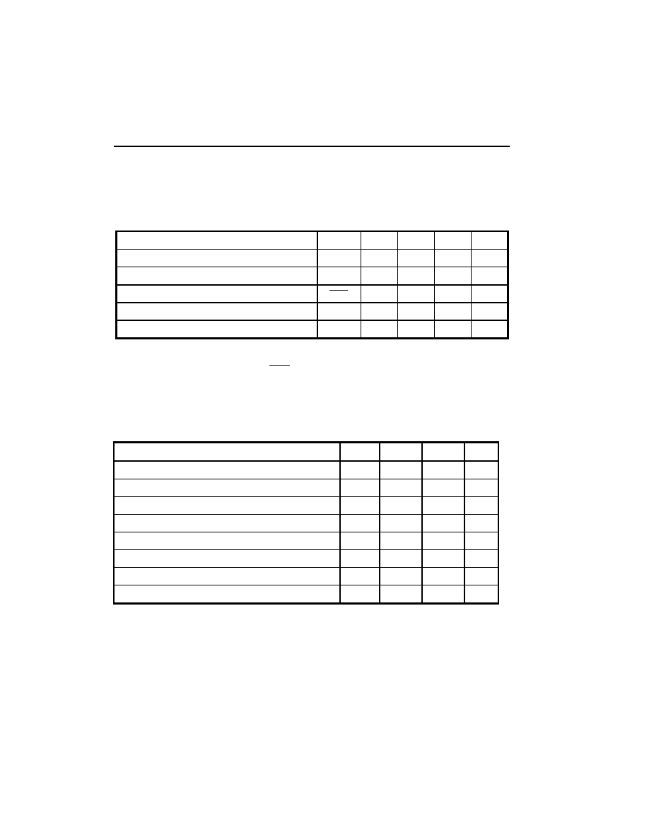
4. ELECTRICAL CHARACTERISTICS
4.1 Recommended operating conditions
Parameter
Symbol
Min.
Typ.
Max.
Units
Power supply voltage
VDD
3.0
3.3
3.6
V
Power supply current
IDD
TBD
mA
Input clock frequency π
XTI
9.99
16.00
MHz
SCL clock frequency
fSCL
450
kHz
Ambient operating temperature
0
70
∞C
Table 1. Recommended operating conditions.
Note 1. When not using a crystal, XTI may be driven from an external source over the
frequency range shown.
4.2 Absolute maximum ratings
Parameter
Symbol
Min.
Max.
Unit
Power supply
VDD
-0.3
+3.6
V
Voltage on input pins (5 v rated)
VI
-0.3
5.5
V
Voltage on input pins (3.3v rated)
VI
-0.3
VDD + 0.3
V
Voltage on output pins (5v rated)
VO
-0.3
5.5
V
Voltage on output pins (3.3v rated)
VO
-0.3
VDD + 0.3
V
Storage temperature
TSTG
-55
150
∫C
Operating ambient temperature
TOP
0
70
∫C
Junction temperature
TJ
125
∫C
Table 2. Maximum operating conditions.
Note: Stresses exceeding these listed under absolute maximum ratings may induce failure.
Exposure to absolute maximum ratings for extended periods may reduce reliability. Functionality
at or above these conditions is not implied.

VP310 PRELIMINARY
DATA
27
4.3 Crystal specification
Parallel resonant fundamental frequency (preferred)
9.99 to 16.00MHz.
Tolerance over operating temperature range
± 25ppm.
Tolerance overall
± 50ppm.
Nominal load capacitance
30pF.
Equivalent series resistance
<35
3 3 p F
3 3 p F
XTI
X T O
G N D
Figure 19. Crystal oscillator circuit.
NOTE: The crystal frequency should be chosen to ensure that the system clock would
marginally exceed the maximum symbol rate required.
4.4 DC electrical characteristics
Parameter
Conditions / Pin
Symbol
Min.
Typ.
Max.
Unit
Operating voltage
VDD
3.0
3.3
3.6
V
Average power supply current
IDD
TBD
mA
Average supply current Stand-by
Mode
TBD
µ
A
Output levels VOH
Tri-state push pull
1 mA drive current.
IIN, QIN, CLKOUT, MDO,
MOVAL, MOSTRT, MCLK,
BKERRB, DISECQ, STATUS
VOH
0.80VDD 0.92VDD
V
Output levels VOL
Tri-state push pull
1 mA drive current,
Pins as VOH.
VOL
0.2
0.4
V
Output level open drain
4 mA drive current.
6 mA drive current.
AGC, SDA, IRQB, GPP<2:0>
0.4
0.6
V
V
Open drain output max. voltage
5.5
V
Input levels VIH CMOS
3.3V input
VIH
0.8VDD
3.6
V
Input levels VIH CMOS
5.0V input
VIH
0.8VDD
5.5
V
Input levels VIL CMOS
VIL
0.2VDD
V
Input leakage Current
VIN = 0 and VDD
10
µ
A
Table 3. DC electrical characteristics.

VP310 PRELIMINARY
DATA
28
4.5 Numerical listing of pin-out
PIN
FUNCTION
PIN
FUNCTION
PIN
FUNCTION
PIN
FUNCTION
1
VSS
21
PLLVDD
41
VSS
61
MDO[1]
2
VDD
22
PLLGND
42
VDD
62
VDD
3
IIN[1]
23
PLL1
43
AGC
63
MDO[2]
4
IIN[0]
24
ADCFGND
44
GPP[0] (SCL2)
64
MDO[3]
5
QIN[5]
25
ADCFVDD
45
GPP[1] (SDA2)
65
MDO[4]
6
QIN[4]
26
VRT
46
GPP[2]
66
MDO[5]
7
QIN[3]
27
IREF
47
DISEQC[1]
67
VDD
8
QIN[2]
28
ISINGP
48
DISEQC[0]
68
MDO[6]
9
VDD
29
COMP
49
RESET 69
MDO[7]
10
VSS
30
ADCDVDD
50
VDD
70
VSS
11
QIN[1]
31
ADCDGND
51
VSS
71
MDOEN
12
QIN[0]
32
VRM
52
STATUS
72
MOVAL
13
VDD
33
QSINGP
53
SCL
73
VDD
14
CLKIN
34
QREF
54
SDA
74
VSS
15
VSS
35
VRB
55
VDD
75
BKERR
16
CLKOUT
36
ADCAGND
56
VSS
76
MOSTRT
17
VDD
37
ADCAVDD
57
IRQ 77
IIN[5]
18
XTI 38
RREF
58
MCLK
78
IIN[4]
19
XTO
39
TEST1
59
MDO[0]
79
IIN[3]
20
VSS
40
TEST2
60
VSS
80
IIN[2]
Table 4. Numerical listing of pin-out.
VP310 PRELIMINARY
DATA
29
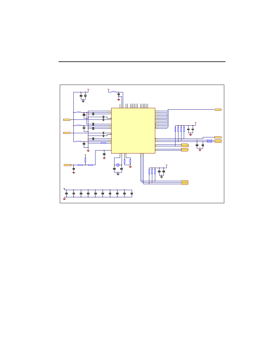
5. APPENDIX 1: Application Schematic
CLKIN
14
CLKOUT
16
PLLVdd
21
PLLGnd
22
PLL1
23
ADCFGnd
24
ADCFVdd
25
VRT
26
IREF
27
ISINGP
28
COMP
29
ADCDVdd
30
ADCDGnd
31
VRM
32
QSINGP
33
QREF
34
VRB
35
ADCAGnd
36
ADCAVdd
37
RREF
38
TEST1
39
TEST2
40
AGC
43
GPP0/SCL OUT
44
GPP1/SDA OUT
45
GPP2
46
DISECQ1/H/V
47
DISECQ0/22kHz
48
RESETB
49
STATUS
52
SCL
53
SDA
54
IRQB
57
MCLK
58
MDO0
59
MDO1
61
MDO2
63
MDO3
64
MDO4
65
MDO5
66
MDO6
68
MDO7
69
MDOENB
71
MOVAL
72
BKERRB
75
MOSTRT
76
IIN5
77
IIN4
78
IIN3
79
IIN2
80
IIN1
3
IIN0
4
QIN5
5
QIN4
6
QIN3
7
QIN2
8
QIN1
11
QIN0
12
XTIB
18
XTO
19
IC1
VP310
XL1
10MHz
C1
33pF
C2
33pF
C3
100nF
C4
100nF
C5
100nF
C6
100nF
C7
100nF
C8
100nF
C9
100nF
C10
100nF
C11
100nF
C12
100nF
Vdd
C13
33n
IFLT
QFLT
AGC
C14
100n
+
C34
22u
Vdd
L1
1u
C15
100n
L2
1u
L3
1u
C16
100n
C17
100n
C18
100n
C19
470n
C20
470n
C21
100n
C22
100n
C23
100n
C24
100n
C25
100n
R1
1k2
R2
100
R3
390
+5V
C26
1n
R4
1k5
R5
10k
R6
10k
SCL2
SDA2
GPP2
R7
1k0
R8
1k0
R9
4k7
C27
100n
C28
1n
+5V
DISECQ1
DISECQ0
+5V
R10
4k7
R11
4k7
R12
4k7
R13 100
R14 100
C29
100p
C30
100p
C31
100n
C32
1n
SCL1
SDA1
RESETB
STATUS
IRQB
R15
4k7
MPEG
C33
100n
L4
1u
Vdd
Figure 20. Application Schematic.


M Mitel (design) and ST-BUS are registered trademarks of MITEL Corporation
Mitel Semiconductor is an ISO 9001 Registered Company
Copyright 1999 MITEL Corporation
All Rights Reserved
Printed in CANADA
TECHNICAL DOCUMENTATION - NOT FOR RESALE
World Headquarters - Canada
Tel: +1 (613) 592 2122
Fax: +1 (613) 592 6909
North America
Asia/Pacific
Europe, Middle East,
Tel: +1 (770) 486 0194
Tel: +65 333 6193
and Africa (EMEA)
Fax: +1 (770) 631 8213
Fax: +65 333 6192
Tel: +44 (0) 1793 518528
Fax: +44 (0) 1793 518581
http://www.mitelsemi.com
Information relating to products and services furnished herein by Mitel Corporation or its subsidiaries (collectively "Mitel") is believed to be reliable. However, Mitel assumes no
liability for errors that may appear in this publication, or for liability otherwise arising from the application or use of any such information, product or service or for any infringement of
patents or other intellectual property rights owned by third parties which may result from such application or use. Neither the supply of such information or purchase of product or
service conveys any license, either express or implied, under patents or other intellectual property rights owned by Mitel or licensed from third parties by Mitel, whatsoever.
Purchasers of products are also hereby notified that the use of product in certain ways or in combination with Mitel, or non-Mitel furnished goods or services may infringe patents or
other intellectual property rights owned by Mitel.
This publication is issued to provide information only and (unless agreed by Mitel in writing) may not be used, applied or reproduced for any purpose nor form part of any order or
contract nor to be regarded as a representation relating to the products or services concerned. The products, their specifications, services and other information appearing in this
publication are subject to change by Mitel without notice. No warranty or guarantee express or implied is made regarding the capability, performance or suitability of any product or
service. Information concerning possible methods of use is provided as a guide only and does not constitute any guarantee that such methods of use will be satisfactory in a specific
piece of equipment. It is the user's responsibility to fully determine the performance and suitability of any equipment using such information and to ensure that any publication or
data used is up to date and has not been superseded. Manufacturing does not necessarily include testing of all functions or parameters. These products are not suitable for use in
any medical products whose failure to perform may result in significant injury or death to the user. All products and materials are sold and services provided subject to Mitel's
conditions of sale which are available on request.