 | –≠–ª–µ–∫—Ç—Ä–æ–Ω–Ω—ã–π –∫–æ–º–ø–æ–Ω–µ–Ω—Ç: VP531ECG | –°–∫–∞—á–∞—Ç—å:  PDF PDF  ZIP ZIP |
The VP531/VP551 converts digital Y, Cr, Cb, data into
analog NTSC/PAL composite video and S-video signals
The outputs are capable of driving doubly terminated 75
ohm loads with standard video levels.
The device accepts data inputs complying with CCIR
Recommendation 601 and 656. The data is time multiplexed
on an 8 bit bus at 27MHz and is formatted as Cb, Y, Cr, Y
(i.e. 4:2:2). The video blanking and sync information from
REC 656 is included in the data stream when the VP531 is
working in slave mode.
The output pixel rate is 27MHz and the input pixel rate
is half this frequency, i.e. 13.5MHz.
All necessary synchronisation signals are generated
internally when the device is operating in master mode. In
slave mode the device will lock to the TRS codes or the HS
and VS inputs.
The rise and fall times of sync, burst envelope and
video blanking are internally controlled to be within
composite video specifications.
Two 9 bit digital to analog converters (DACs) are used
to convert the digital luminance and chrominance data into
analog signals. An inverted composite video signal is
generated by summing the complementary current outputs
of each DAC. An internally generated reference voltage
provides the biasing for the DACs.
FEATURES
s
Converts Y, Cr, Cb data to analog composite video and
S-video
s
Supports CCIR recommendations 601 and 656
s
All digital video encoding
s
Selectable master/slave mode for sync signals
s
Switchable chrominance bandwidth
s
Switchable pedestal with gain compensation
s
SMPTE 170M NTSC or CCIR 624 PAL compatible
outputs
s
GENLOCK mode
s
I
2
C bus serial microprocessor interface
s
VP531E supports Macrovision anti-taping format REV
6.1 in PAL and REV 7.01 in NTSC
APPLICATIONS
s
Digital Cable TV
s
Digital Satellite TV
s
Multi-media
s
Video games
s
Karaoke
s
Digital VCRs
ORDERING INFORMATION
VP531E/CG/GP1N
VP551E/CG/GP1N
PIN
FUNCTION
PIN
FUNCTION
1
VDD
33
VDD
2
GND
34
RESET
3
D0 (VS I/O)
35
REFSQ
4
D1 (HS I/O)
36
GND
5
D2 (FC0 O/P)
37
VDD
6
D3 (FC1 O/P)
38
GND
7
D4 (FC2 O/P)
39
PD7
8
D5
40
PD6
9
D6 (SCSYNC I/P)
41
PD5
10
D7 (PALID I/P)
42
PD4
11
GND
43
PD3
12
VDD
44
PD2
13
GND
45
PD1
14
GND
46
PD0
15
PXCK
47
GND
16
VDD
48
VDD
17
CLAMP
49
AGND
18
COMPSYNC
50
VREF
19
GND
51
DACGAIN
20
VDD
52
COMP
21
TDO
53
AVDD
22
TDI
54
LUMAOUT
23
TMS
55
AGND
24
TCK
56
COMPOUT
25
GND
57
AGND
26
SA1
58
CHROMAOUT
27
SA2
59
AVDD
28
SCL
60
N/C
29
VDD
61
N/C
30
SDA
62
AVDD
31
GND
63
AVDD
32
VDD
64
N/C
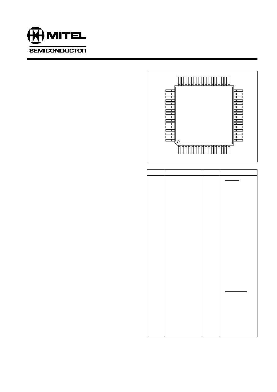
Fig.1 Pin connections (top view)
GP64
PIN 64
PIN 1
VP531E/VP551E
NTSC/PAL Digital Video Encoder
Advance Information
Supersedes DS4573 1.4 May 1997 edition
DS4573 - 2.3 October1998

VP531E/VP551E
2
66.83
1.050
27k
1.3699
24.93
80
33.75
17.64
1.40
7.62
7.62
0.40
34.15
18.71
8.02
8.02
0.00
ELECTRICAL CHARACTERISTICS
Test conditions (unless otherwise stated): As specified in Recommended Operating Conditions
DC CHARACTERISTICS
VIN
VIL
VIH
VIL
IIH
IIL
VOH
VOL
VOL
2.0
0.7 VDD
3.7
0.8
0.3 VDD
10
-10
0.4
0.6
V
V
V
V
µ
A
µ
A
V
V
V
Parameter
Conditions
VIN = VDD
VIN = VSS
IOH = -1mA
IOL = +4mA
IOL = +6mA
Symbol
Min.
Typ.
Max.
Units
ELECTRICAL CHARACTERISTICS
Test conditions (unless otherwise stated): As specified in Recommended Operating Conditions
DC CHARACTERISTICS DACs
INL
DNL
V
REF
Z
R
I
REF
K
DAC
±
1.5
±
1
±
5
LSB
LSB
% grey
µ
A
V
mA
pV-s
mA
mA
mA
mA
mA
mA
mA
mA
mA
mA
mA
Parameter
Symbol
Min.
Typ.
Max.
Units
Accuracy (each DAC)
Integral linearity error
Diffential linearity error
DAC matching error
Monotonicity
LSB size
Internal reference voltage
Internal reference voltage output impedance
Reference Current (V
REF
/R
REF
) R
REF
= 769
DAC Gain Factor (V
OUT
= K
DAC
x I
REF
x R
L
). V
OUT
= DAC code 511
Peak Glitch Energy (see fig.8)
CVBS (see note), Y and C - NTSC (pedestal enabled)
Maximum output, relative to sync bottom
White level relative to black level
Black level relative to blank level
Blank level relative to sync level
Colour burst peak - peak
DC offset (bottom of sync)
CVBS, Y and C - PAL
Maximum output
White level relative to black level
Black level relative to sync level
Colour burst peak - peak
DC offset (bottom of sync)
Digital Inputs TTL compatible (except SDA, SCL)
Input high voltage
Input low voltage
Digital Inputs SDA, SCL
Input high voltage
Input low voltage
Input high current
Input low current
Digital Outputs CMOS compatible
Output high voltage
Output low voltage
Digital Output SDA
Output low voltage
guaranteed
Note: For the inverted CVBS output subtract the above currents from the maximum output (DAC code 511 = 34.12mA).
All figures are for: R
REF
= 769
, R
L
= 37.5
. When the device is set up in NTSC mode there is a +0.25% error in the PAL levels.
If R
L
= 75
then R
REF
= 1538
VP531E/VP551E
3
ABSOLUTE MAXIMUM RATINGS
Supply voltage
VDD, AVDD
-0∑3 to 7∑0V
Voltage on any non power pin
-0∑3 to VDD+0∑3V
Ambient operating temperature
0 to 70
∞
C
Storage temperature
-55
∞
C to 150
∞
C
Note: Stresses exceeding these listed under Absolute
Maximum Ratings may induce failure. Exposure to Absolute
Maximum Ratings for extended periods may reduce
reliability. Functionality at or above these conditions is not
implied.
RECOMMENDED OPERATING CONDITIONS
Parameter
Min.
Typ.
Max.
Units
Power supply voltage
Power supply current (including analog outputs)
Input clock frequency
SCL clock frequency
Analog video output load
DAC gain resistor
Ambient operating temperature
Symbol
VDD, AVDD
IDD
PXCK
fscl
4.75
-50ppm
0
5.25
+50ppm
500
70
V
mA
MHz
kHz
∞
C
5.00
150
27.00
37.5
769
VIDEO CHARACTERISTICS
Parameter
-61
-56
-58
2.5
2.5
Max.
Symbol
Min.
Typ.
5.5
1.3
650
3.57954545
4.43361875
3.58205625
9
10
300
145
245
1.5
0.5
-60
10
MHz
MHz
kHz
MHz
MHz
MHz
Fsc cycles
Fsc cycles
ns
ns
ns
% pk-pk
∞
pk-pk
dB
dB
dB
%
%
dB
ns
Units
ESD COMPLIANCE
Pins
All pins
All pins
Notes
Meets Mil-Std-883 Class 2
Test Levels
2kV on 100pF through 1k5
200V on 200pF through 0
& 500nH
Test
Human body model
Machine model
Luminance bandwidth
Chrominance bandwidth (Extended B/w mode)
Chrominance bandwidth (Reduced B/w mode)
Burst frequency (NTSC)
Burst frequency (PAL-B, D,G, H, I)
Burst frequency (PAL-N Argentina)
Burst cycles (NTSC and PAL-N)
Burst cycles (NTSC and PAL-B, D, G, H,I)
Burst envelope rise / fall time (NTSC and PAL-B, D, G, H,I)
Analog video sync rise / fall time (NTSC and PAL-N)
Analog video blank rise / fall time (NTSC and PAL-B, D, G, H,I)
Differential gain
Differential phase
Signal to noise ratio (unmodulated ramp)
Chroma AM signal to noise ratio (100% red field)
Chroma PM signal to noise ratio (100% red field)
Hue accuracy
Colour saturation accuracy
Residual sub carrier
Luminance / chrominance delay
VP531E/VP551E
4
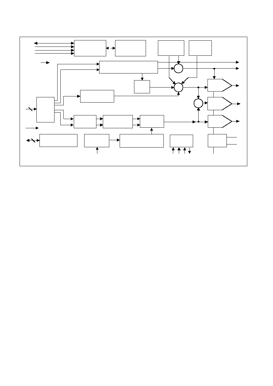
Figure 2 VP531E Functional block diagram, VP551E is identical except there is no Anti-Taping Control
I
2
C INTERFACE
SET-UP
REGISTERS
ANTI-TAPING
CONTROL
VIDEO TIMING GENERATOR
COLOUR SUBCARRIER
GENERATOR
MODULATOR
CHROMA
LOW -PASS
FILTER
INPUT
DEMUX
8
8
PD7-0
D7-0
PXCK
SDA
SCL
SA1
SA2
Y
Cr
Cb
SYNC
BLANK
INSERT
LUMA OUT
COMP
CHROMA OUT
INTERPOLATOR
INTERPOLATOR
JTAG.
GENERAL
PURPOSE PORT
&
CHROMA
INTERP
RESET
CLAMP
CHROMA
DAC
COMP
DAC
OUT
TDI
TMS TCK
TDO
+
DAC
REF
VREF
+
REFSQ
DIGITAL
PHASE COMP
CLOSED
CAPTION
+
DACGAIN
COMP
COMPSYNC
LUMA
DAC
VP531E/VP551E
5
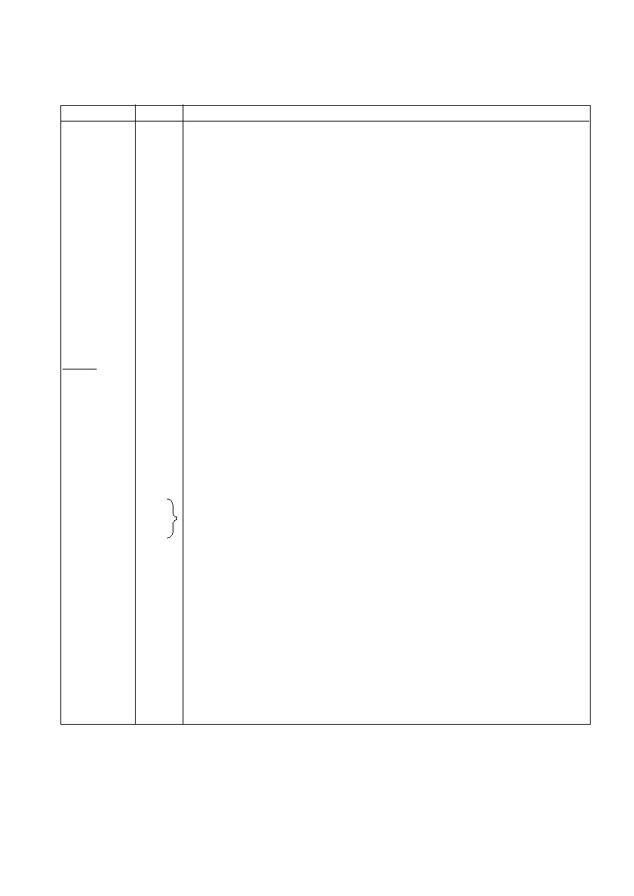
Pin Name
Pin No.
Description
PD0-7
39 - 46
8 Bit Pixel Data inputs clocked by PXCK. PD0 is the least significant bit, corresponding to Pin
46. These pins are internally pulled low.
D0-7
3 - 10
8 Bit General Purpose Port input/output. D0 is the least significant bit, corresponding to Pin 3.
These pins are internally pulled low.
PXCK
15
27MHz Pixel Clock input. The VP531 internally divides PXCK by two to provide the pixel
clock.
CLAMP
17
The CLAMP output signal is synchronised to COMPSYNC output and indicates the position of
the BURST pulse, (lines 10-263 and 273-525 for NTSC; lines 6-310 and 319-623 for PAL-
B,D, G,I,N(Argentina)).
COMPSYNC
18
Composite sync pulse output. This is an active low output signal.
TDO
21
JTAG Data scan output port.
TDI
22
JTAG Data scan input port.
TMS
23
JTAG Scan select input.
TCK
24
JTAG Scan clock input.
SA1
26
Slave address select.
SA2
27
Slave address select.
SCL
28
Standard I
2
C bus serial clock input.
SDA
30
Standard I
2
C bus serial data input/output.
RESET
34
Master reset. This is an asynchronous active low input signal and must be asserted for a
minimum of 200ns in order to reset the VP531/VP551.
REFSQ
35
Reference square wave input used only during Genlock mode.
VREF
50
Voltage reference output. This output is nominally 1∑055V and should be decoupled with a
100nF capacitor to GND.
DAC GAIN
51
DAC full sacle current control. A resistor connected between this pin and GND sets the
magnitude of the video output current. An internal loop amplifier control a reference current
flowing through this resistor so that the voltage across it is equal to the Vref voltage.
COMP
52
DAC compensation. A 100nF ceramic capacitor must be connected between pin 52 and pin
53.
LUMAOUT
54
True luminance, true chrominance and inverted composite video signal outputs. These are
COMPOUT
56
high impedance current source outputs. A DC path to GND must exist from each of these
CHROMAOUT
58
pins
NOT USED
60, 61, 64
VDD
1, 12, 16,
Positive supply input. All VDD pins must be connected.
20, 29,
32, 33,
37, 48
AVDD
53, 59
Analog positive supply input. All AVDD pins must be connected.
62, 63
GND
2, 11, 13,
Negative supply input. All GND pins must be connected.
14, 19,
25, 31,
36, 38, 47
AGND
49, 55, 57
Negative supply input. All AGND pins must be connected.
PIN DESCRIPTIONS