 | –≠–ª–µ–∫—Ç—Ä–æ–Ω–Ω—ã–π –∫–æ–º–ø–æ–Ω–µ–Ω—Ç: 32174 | –°–∫–∞—á–∞—Ç—å:  PDF PDF  ZIP ZIP |

Description
The M32170 and M32174 Group are 32-bit single chip RISC
microcomputers designed for use in general industrial and
household equipment.
These microcomputers contains a variety of peripheral
functions ranging from16-channel A-D converters to 64chan-
nel multifunction timers, 10-channel DMAs, 6-channel serial
I/Os, 1-channel real time debugger, 1-channel Full-CAN, and
JTAG (boundary scan facility).
With lower power consumption and low noise characteristics
also considered, these microcomputers are ideal for embed-
ded equipment applications.
Features
M32R RISC CPU core
∑ Uses the M32R family RISC CPU core (Instruction set
common to all microcomputers in the M32R family)
∑ Five-stage pipelined processing
∑ Sixteen 32-bit general-purpose registers
∑ 16-bit/32-bit instructions implemented
∑ DSP function instructions (sum-of-products calculation
using 56-bit accumulator)
∑ Built-in flash memory
∑ Built-in flash programming boot program
∑ Built-in RAM
∑ PLL clock generating circuit ........... Built-in
◊
4 PLL circuit
∑ Maximum operating frequency of the CPU clock
40MHz(when operating at -40 to +85
o
C)
32MHz(when operating at -40 to +125
o
C)
Table 1 32170 Group Name List by type
Type Name
RAM Size
ROM Size
Package
M32170F6VFP
40K bytes
768K bytes
240QFP
M32170F4VFP
32K bytes
512K bytes
240QFP
M32170F3VFP
32K bytes
384K bytes
240QFP
M32170F6VWG
40K bytes
768K bytes
255FBGA
M32170F4VWG
32K bytes
512K bytes
255FBGA
M32170F3VWG
32K bytes
384K bytes
255FBGA
Note: 255FBGA is currently under development.
Table 2 32170 Group Name List by type
Type Name
RAM Size
ROM Size
Package
M32174F4VFP
40K bytes
512K bytes
240QFP
M32174F3VFP
40K bytes
384K bytes
240QFP
M32174F4VWG
40K bytes
512K bytes
255FBGA
M32174F3VWG
40K bytes
384K bytes
255FBGA
Note: 255FBGA is currently under development.
64-channel multijunction timers (MJT)
Multifunction timers are incorporated that support various
purposes of use.
16-bit output related timers ....................................... 35ch
16-bit input/output related timers .............................. 10ch
16-bit input related timers ......................................... 11ch
32-bit input related timers .......................................... 8ch
∑ Flexible configuration is possible through interconnection
of timers.
∑ The internal DMAC and A-D converter can be started by a
timer.
Real-time Debugger
∑ Includes dedicated clock-synchronized serial I/O that can
read and write the contents of the internal RAM independently
of the CPU.
∑ Can look up and update the data table in real time while the
program is running.
∑ Can generate a dedicated interrupt based on RTD commu-
nication.
Abundant internal peripheral functions
In addition to the timers and real-time debugger, the micro-
computer contains the following peripheral functions.
∑ DMAC .............................................................. 10 channels
∑ Two independent
A-D converter .............. (10-bit converter
◊
16 channels)
◊
2
∑ Serial I/O ............................................................ 6 channels
∑ Interrupt controller ........... 31 interrupt sources, 8 priority levels
∑ Wait controller
∑ Full CAN .............................................................. 1 channel
∑ JTAG (boundary scan function)
Designed to operate at high temperatures
To meet the need for use at high temperatures, the micro-
computer is designed to be able to operate in the temperature
range of -40 to +125
o
C when CPU clock operating
frequency = 32 MHz. When CPU clock operating frequency =
40 MHz, the microcomputer can be used in the temperature
range of -40 to +85
o
C.
Note: This does not guarantee continuous operation at
125
o
C. If you are considering use of the microcom
puter at 125
o
C, please consult Mitsubishi.
Applications
Automobile equipment control (e.g., Engine, ABS, AT), indus-
trial equipment system control, and high-function OA equip-
ment (e.g., PPC)
Mitsubishi Microcomputers
SINGLE-CHIP 32-BIT CMOS MICROCOMPUTER
32170 Group, 32174 Group
2001-5-14 Rev.1.0
Mitsubishi Microcomputers
2
2001-5-14 Rev.1.0
SINGLE-CHIP 32-BIT CMOS MICROCOMPUTER
32170 Group, 32174 Group
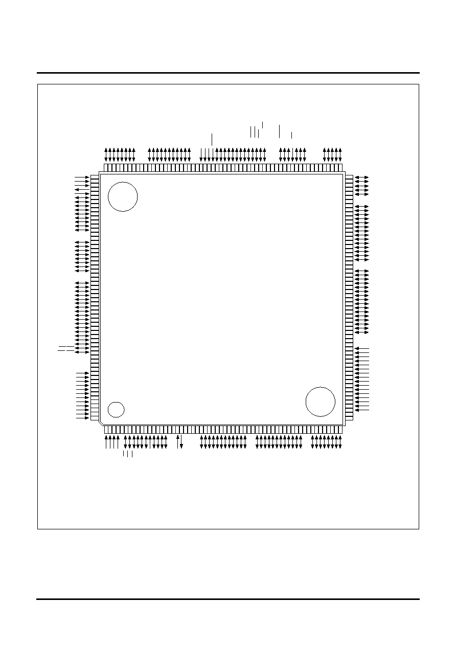
Figure 1 Pin Layout Diagram of the 240QFP
Pin Assignment(top view)
Package 240P6Y-A
M32170F3VFP
M32170F4VFP
M32170F6VFP
2
4
3
44
43
5
6
7
8
9
35
36
37
38
39
40
22
23
24
25
26
27
2
8
2
9
30
31
32
33
34
11
12
13
1
4
15
16
17
18
19
20
21
41
42
10
1
60
59
51
52
53
54
55
56
45
46
47
48
49
50
57
58
89
90
99
98
97
96
95
94
93
92
91
103
102
101
112
111
110
109
108
107
106
105
104
120
119
118
117
116
115
114
113
63
64
66
67
68
69
70
71
72
73
74
65
84
75
76
77
78
79
80
81
82
83
85
86
87
88
61
62
100
12
4
132
130
12
9
127
121
137
14
6
14
5
144
1
43
142
141
14
0
13
9
13
8
1
55
1
54
15
3
1
52
1
51
1
50
149
148
147
15
6
1
59
1
58
157
133
136
13
5
13
4
123
122
131
12
8
12
6
12
5
1
66
165
16
4
1
63
162
1
61
17
5
17
4
173
172
171
170
169
16
8
1
67
176
179
178
177
1
60
180
195
185
184
183
182
181
186
189
188
187
194
193
192
191
190
196
199
198
197
205
204
203
202
201
200
206
209
208
207
215
214
213
212
211
210
216
239
217
219
218
225
224
223
222
221
220
226
227
229
228
230
235
234
233
232
231
236
237
238
240
P41/BLW/BLE
P157/TIN7
P156/TIN6
P155/TIN5
P154/TIN4
P153/TIN3
P152/TIN2
P151/TIN1
P150/TIN0
P147/TIN15
P146/TIN14
P145/TIN13
P144/TIN12
P143/TIN11
P142/TIN10
P141/TIN9
P140/TIN8
VSS
VCCE
P137/TIN23
P136/TIN22
P135/TIN21
P134/TIN20
P133/TIN19
P132/TIN18
P131/TIN17
P130/TIN16
VSS
VCCI
P42/BHW/BHE
P127/TCLK3
P126/TCLK2
P125/TCLK1
P124/TCLK0
P107/TO15
P106/TO14
P105/TO13
P104/TO12
VSS
V
CCI
P103/TO11
VSS
VCCI
P4
3/RD
P44
/CS
0
P45/
CS1
P14
/DB12
P37
/A22
P36/
A21
P33/
A18
P31
/A16
P30
/A1
5
P35
/A20
P3
4/
A19
P32
/A17
V
CCE
P27
/A30
P2
5/A2
8
P2
6/A2
9
P2
4/A
27
P07
/DB7
P02
/D
B2
P01/
DB1
P00
/DB0
P23
/A
26
P22
/A25
P20
/A23
P10
/D
B8
P11
/DB
9
V
SS
P15/
DB13
P13
/DB11
P12
/DB
10
P06
/DB
6
P0
4/D
B4
P03
/D
B3
P47
/A14
P21
/A24
P46/
A13
VCC
E
V
SS
P16
/DB1
4
P17
/DB1
5
P82/TXD0
VSS
VCCE
P172/TIN24
P173/TIN25
P174/TXD2
P175/RXD2
P176/TXD3
P177/RXD3
P160/TO21
P161/TO22
P162/TO23
P163/TO24
P164/TO25
P165/TO26
P166/TO27
P167/TO28
VSS
VCCI
VREF0
AVCC0
AD0IN7
AD0IN6
AD0IN5
AD0IN4
AD0IN3
AD0IN2
AD0IN1
AD0IN0
AD0IN15
AD0IN14
AD0IN13
AD0IN12
AD0IN11
AD0IN10
AD0IN9
AD0IN8
AVSS0
P181/TO30
P182/TO31
P183/TO32
P184/TO33
P180/TO29
VSS
VCCE
P186/TO35
P187/TO36
P190/TIN26
P185/TO34
P194/TIN30
P195/TIN31
P196/TIN32
P197/TIN33
P191/TIN27
P192/TIN28
P193/TIN29
RE
SET
P84/SCLKI0/SCLKO0
P83/RXD0
P85/TXD1
P86/RXD1
P
87/S
CLK
I1/S
CLK
O1
V
SS
V
CCE
VCC
I
P6
2
VSS
FP
P67
/ADT
RG
P66
/SC
LKI5
/SCL
KO
5
P6
5/SC
LKI4
/SC
LK
O
4
P9
4/T
O
17
P7
4/R
TDT
XD
P7
5/R
TDR
XD
P7
6/R
TD
A
CK
P77
/R
T
DC
LK
P
61
P6
3
P11
4/T
O
4
P115
/T
O
5
P11
6/T
O
6
P117
/T
O
7
V
SS
V
CCE
MO
D1
P100
/T
O
8
P101
/T
O
9
P102
/T
O10
P110
/T
O
0
P111
/T
O
1
P112
/T
O
2
P113
/T
O
3
P95
/T
O
18
P96
/T
O1
9
P97
/T
O20
P70
/BCL
K/W
R
P71/W
AIT
P72
/
HRE
Q
P6
4/SB
I
MO
D0
P9
3/T
O
16
P73
/
HA
C
K
VCC
I
V
SS
V
DD
FV
CC
P201
/RX
D4
P202
/TX
D5
P203
/RX
D5
P200
/TX
D4
AD1IN5
AD1IN4
AD1IN3
AD1IN2
AD1IN1
AD1IN0
VREF1
AD1IN15
AD1IN14
AD1IN13
AD1IN12
AV
SS1
AD1IN6
JTDO
JTRST
JTCK
JTMS
JTDI
P212
/T
O3
9
P213
/T
O4
0
P21
4/T
O41
P21
5/T
O42
P211
/T
O
38
P210
/T
O
37
P21
6/T
O43
P217
/T
O44
VC
NT
OSC
-VCC
X
OUT
X
IN
OSC
-VSS
P221
/CR
X
P220
/CT
X
V
SS
VSS
P0
5/DB
5
AD1IN11
AD1IN10
AD1IN9
AD1IN8
AD1IN7
P222
P223
(N
ote)
P22
4/A11
(Note)
P22
5/A
12
VSS
AVCC1
M32174F3VFP
M32174F4VFP
Note: Use caution when using these pins because they nave a debug event function.

Mitsubishi Microcomputers
3
SINGLE-CHIP 32-BIT CMOS MICROCOMPUTER
2001-5-14 Rev.1.0
32170 Group, 32174 Group
Figure 2 Pin Layout Diagram of the 255FBGA
Package 255FBGA
A
B
C
D
E
F
G
H
J
K
L
M
N
P
R
T
U
V
W
Y
1
2
3
4
5
6
7
8
9
10
11
12
13
14
15
16
17
18
19
20
AD1IN12
AD1IN13
AD1IN14
AD1IN15
AVSS1
P43
/RD
P44
/CS0
P45
/CS1
P46
/A13
P47
/A14
P220
/CTX
P221
/CRX
P222
P223
P224
/A11
P225
/A12
VSS
OSC-
VSS
XIN
XOUT
OSC-
VCC
VSS
VCNT
VSS
P30
/A15
P31
/A16
P32
/A17
P33
/A18
P34
/A19
P35
/A20
TRCLK
TRSYNC
P36
/A21
P37
/A22
P20
/A23
P21
/A24
P23
/A26
P22
/A25
VCCE
VSS
P24
/A27
P25
/A28
P26
/A29
P27
/A30
P00
/DB0
P01
/DB1
P02
/DB2
P03
/DB3
P04
/DB4
P05
/DB5
P06
/DB6
P07
/DB7
VCCE
VSS
P10
/DB8
P11
/DB9
P12
/DB10
P13
/DB11
P14
/DB12
P15
/DB13
P16
/DB14
P17
/DB15
VREF0
AVCC0
AD0IN0
AD0IN1
AD0IN2
AD0IN3 AD0IN4
AD0IN5
AD0IN6
AD0IN7 AD0IN8
AD0IN9
AD0IN10
AD0IN11 AD0IN12
AD0IN13
AD0IN14
AD0IN15 AVSS0
VCCE
VSS
P180
/TO29
P181
/TO30
P182
/TO31
P183
/TO32
P184
/TO33
P185
/TO34
P186
/TO35
P187
/TO36
P190
/TIN26
P191
/TIN27
P192
/TIN28
P193
/TIN29
P194
/TIN30
P196
/TIN32
P195
/TIN31
P197
/TIN33
VCCI
VSS
P160
/TO21
P161
/TO22
P162
/TO23
P163
/TO24
P164
/TO25
P165
/TO26
P166
/TO27
P167
/TO28
P172
/TIN24
P173
/TIN25
P174
/TXD2
P175
/RXD2
P176
/TXD3
P177
/RXD3
VCCE
VSS
P82
/TXD0
P87
/SCLK1
P84
/SCLK0
P85
/TXD1
P86
/RXD1
TRDATA
0
TRDATA
1
TRDATA
2
TRDATA
3
P200
/TXD4
P201
/RXD4
P202
/TXD5
P203
/RXD5
VCCI
VSS
P83
/RXD0
VSS
P61
P62
FVCC
P64
/SBI
P65
/SCLK4
P66
/SCLK5
P63
VCCI
VSS
VCCE
P67
/ADTRG
P71
/WAIT
P72
/HREQ
P73
/HACK
P74/
RTDTXD
P75/
RTDRXD
P76/
RTDACK
P77/
RTDCLK
P93
/TO16
P94
/TO17
P95
/TO18
P96
/TO19
P97
/TO20
RESET
MOD0
MOD1
FP
VCCE
VSS
P110
/TO0
P111
/TO1
P112
/TO2
P113
/TO3
TRDATA
4
TRDATA
5
TRDATA
6
TRDATA
7
P114
/TO4
P115
/TO5
P116
/TO6
P117
/TO7
P100
/TO8
P101
/TO9
P102
/TO10
VDD
VCCI
VSS
P210
/TO37
P211
/TO38
P212
/TO39
P214
/TO41
P215
/TO42
P213
/TO40
P216
/TO43
P217
/TO44
JDBI
JTCK
JEVENT
0
JTRST
JEVENT
1
JTDO
JTDI
P103
/TO11
P104
/TO12
P105
/TO13
P106
/TO14
P107
/TO15
P124
/TCLK0
P125
/TCLK1
P126
/TCLK2
P127
/TCLK3
VCCI
VSS
P130
/TIN16
P131
/TIN17
P132
/TIN18
P133
/TIN19
P134
/TIN20
P135
/TIN21
P136
/TIN22
P137
/TIN23
VCCE
VSS
P140
/TIN8
P141
/TIN9
P142
/TIN10
P143
/TIN11
P144
/TIN12
P145
/TIN13
P146
/TIN14
P147
/TIN15
P150
/TIN0
P151
/TIN1
P152
/TIN2
P153
/TIN3
P154
/TIN4
P155
/TIN5
P156
/TIN6
P157
/TIN7
P41
/BLW
P42
/BHW
VCCI
VSS
VREF1 AVCC1
AD1IN0
AD1IN1
AD1IN2 AD1IN3
AD1IN4
AD1IN5
AD1IN6 AD1IN7
AD1IN8 AD1IN10
AD1IN9 AD1IN11
M32170F3VWG
M32170F4VWG
M32170F6VWG
M32174F3VWG
M32174F4VWG
P70
/BCLK
JTMS
N.C
N.C
Pin Assignment(top view)
Note 1: NC pin (W19, Y1) shows non-connect. Be open state.
Note 2: Use caution when using P224/A11 and P225/A12 because they have a debug event function.
Note 3: 255FBGA is currently under development.
Mitsubishi Microcomputers
4
2001-5-14 Rev.1.0
SINGLE-CHIP 32-BIT CMOS MICROCOMPUTER
32170 Group, 32174 Group
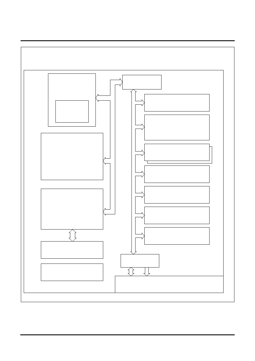
Figure 3 Block diagram
PLL clock generation
circuit
Internal bus
interface
Address
Data
Internal RAM
( M32170F6 : 40KB )
( M32170F4 : 32KB )
( M32170F3 : 32KB )
Internal flash memory
( M32170F6 : 768KB )
( M32170F4 : 512KB )
( M32170F3 : 384KB )
M32R CPU core
(max 40MHz)
Multiplier-
accumulator
(32
◊
16 + 56)
DMAC
(10 channels)
Multijunction timer
(MJT : 64 channels)
Serial I/O
(6 channels)
A-D converter
(10-bit, 16 channels)
◊
2
Wait controller
Interrupt controller
(31 sources, 8 levels)
Real-time debugger
(RTD)
External bus
interface
Inter
nal
16-bit b
us
Inter
nal
32-bit b
us
Input/output port(JTAG) 157 lines
Full CAN
(1 channel)
32170/32174
( M32174F4 : 512KB )
( M32174F3 : 384KB )
( M32174F4 : 40KB )
( M32174F3 : 40KB )

Mitsubishi Microcomputers
5
SINGLE-CHIP 32-BIT CMOS MICROCOMPUTER
2001-5-14 Rev.1.0
32170 Group, 32174 Group
Table 3 Outline Performance (1/2)
Functional Block
Features
M32R CPU core
M32R family CPU core, internally configured in 32 bits
Built-in multiplier-accumulator (32
◊
16 + 56)
Basic bus cycle : 25 ns (Internal CPU clock frequency at 40 MHz, Internal peripheral
clock frequency at 20 MHz)
Logical address space : 4G bytes, linear
General-purpose register : 32-bit register
◊
16, Control register: 32-bit register
◊
5
accumulator : 56 bits
External data bus
16 bits data bus
Instruction set
16-bit/32-bit instruction formats
83 instructions/ 9 addressing modes
Internal flash memory
M32170F6 : 768K bytes
M32170F4, M32174F4 : 512K bytes
M32170F3, M32174F3 : 384K bytes
Rewrite durability : 100 times
Internal RAM
M32170F6, M32174F4, M32174F3 : 40K bytes
M32170F4, M32170F3 : 32K bytes
DMAC
10 channels (DMA transfers between internal peripheral I/Os, between internal peripheral
I/O and internal RAM, and between internal RAMs)
Channels can be cascaded and can operate in combination with internal peripheral I/O
Multijunction timer
64 channels of multijunction timers.
∑ 16-bit output-related timers
◊
35 channels (single-shot, delayed single-shot, PWM, single-shot PWM)
∑ 16-bit input/output-related timers
◊
10 channels (event count mode, single-shot, PWM, measurement)
∑ 16-bit input-related timers
◊
11 channels (measurement, event count mode, multiply-by-4 count 3 channels)
∑ 32-bit input-related timers
◊
8 channels (measurement)
Flexible timer configuration is possible through interconnection of channels using the event bus.
A-D converter
2 independent 10-bit multifunction A-D converters
∑ Input 16 channels
◊
2
∑ Scan-based conversion can be switched with 4, 8, and 16
∑ Capable of interrupt conversion during scan
∑ 8-bit/10-bit readout function available
Serial I/O
6 channels (The serial I/Os can be set for synchronous serial I/O or UART.
SIO2,3 are UART mode only)
Real-time debugger (RTD)
1-channels dedicated clock-synchronized serial
The entire internal RAM can be read or rewritten from the outside without CPU intervention.
Interrupt controller
Controls interrupts from internal peripheral I/Os
(Priority can be set to one of 8 levels including interrupt disabled)
Wait controller
Controls wait when accessing external extended area
(1 to 4 wait cycles inserted + prolonged by external WAIT signal input)
CAN
16-channels message slots
JTAG
Boundary-Scan function