MITSUBISHI
ELECTRIC
-1-
M2S12D20/ 30TP -75, -75L, -10, -10L
Feb. '02
MITSUBISHI LSIs
DDR SDRAM (Rev.1.1)
512M Double Data Rate Synchronous DRAM
MITSUBISHI ELECTRIC
DESCRIPTION
M2S12D20TP is a 4-bank x 33,554,432-word x 4-bit,
M2S12D30TP is a 4-bank x 16,777,216-word x 8-bit,
double data rate synchronous DRAM, with SSTL_2 interface. All control and address signals are
referenced to the rising edge of CLK. Input data is registered on both edges of data strobes, and
output data and data strobe are referenced on both edges of CLK. The M2S12D20/30TP achieve
very high speed data rate up to 133MHz, and are suitable for main memory in computer systems.
FEATURES
- Vdd=Vddq=2.5V+0.2V
- Double data rate architecture; two data transfers per clock cycle
- Bidirectional, data strobe (DQS) is transmitted/received with data
- Differential clock inputs (CLK and /CLK)
- DLL aligns DQ and DQS transitions
- Commands are entered on each positive CLK edge;
- data and data mask are referenced to both edges of DQS
- 4 bank operations are controlled by BA0, BA1 (Bank Address)
- /CAS latency- 2.0/2.5 (programmable)
- Burst length- 2/4/8 (programmable)
- Burst type- sequential / interleave (programmable)
- Auto precharge / All bank precharge is controlled by A10
- 8192 refresh cycles /64ms (4 banks concurrent refresh)
- Auto refresh and Self refresh
- Row address A0-12 / Column address A0-9,11-12(x4)/ A0-9,11(x8)
SSTL_2 Interface
- 400-mil, 66-pin Thin Small Outline Package (TSOP II)
- JEDEC standard
- Low Power for the Self Refresh Current ICC6 :4mA (-75L,-10L)
125MHz
100MHz
-10 / -10L
CL=2.5 *
CL=2 *
133MHz
100MHz
-75 / -75L
Clock Rate
Speed Grade
Operating Frequencies
* CL = CAS(Read) Latency
Contents are subject to change without notice.
MITSUBISHI
ELECTRIC
-2-
M2S12D20/ 30TP -75, -75L, -10, -10L
Feb. '02
MITSUBISHI LSIs
DDR SDRAM (Rev.1.1)
512M Double Data Rate Synchronous DRAM
MITSUBISHI ELECTRIC
CLK,/CLK
: Master Clock
CKE
: Clock Enable
/CS
: Chip Select
/RAS
: Row Address Strobe
/CAS
: Column Address Strobe
/WE
: Write Enable
DQ0-7
: Data I/O
DQS
: Data Strobe
DM
: Write Mask
Vref
: Reference Voltage
1
2
3
4
5
6
7
8
9
10
11
12
13
14
15
16
17
18
19
20
21
22
23
24
25
26
27
28
29
30
31
32
33
66
65
64
63
62
61
60
59
58
57
56
55
54
53
52
51
50
49
48
47
46
45
44
43
42
41
40
39
38
37
36
35
34
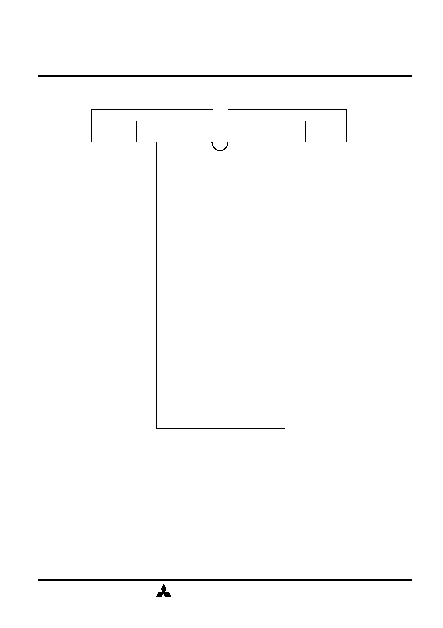
66pin TSOP(II)
400mil width
x
875mil length
0.65mm
Lead Pitch
ROW
A0-12
Column
A0-9,11-12(x4)
A0-9,11 (x8)
VDD
DQ0
VDDQ
NC
DQ1
VSSQ
NC
DQ2
VDDQ
NC
DQ3
VSSQ
NC
NC
VDDQ
NC
NC
VDD
NC
NC
/WE
/CAS
/RAS
/CS
NC
BA0
BA1
A10/AP
A0
A1
A2
A3
VDD
VSS
DQ7
VSSQ
NC
DQ6
VDDQ
NC
DQ5
VSSQ
NC
DQ4
VDDQ
NC
NC
VSSQ
DQS
NC
VREF
VSS
DM
/CLK
CLK
CKE
NC
A12
A11
A9
A8
A7
A6
A5
A4
VSS
A0-12
: Address Input
BA0,1
: Bank Address Input
Vdd
: Power Supply
VddQ
: Power Supply for Output
Vss
: Ground
VssQ
: Ground for Output
VSS
NC
VSSQ
NC
DQ3
VDDQ
NC
NC
VSSQ
NC
DQ2
VDDQ
NC
NC
VSSQ
DQS
NC
VREF
VSS
DM
/CLK
CLK
CKE
NC
A12
A11
A9
A8
A7
A6
A5
A4
VSS
VDD
NC
VDDQ
NC
DQ0
VSSQ
NC
NC
VDDQ
NC
DQ1
VSSQ
NC
NC
VDDQ
NC
NC
VDD
NC
NC
/WE
/CAS
/RAS
/CS
NC
BA0
BA1
A10/AP
A0
A1
A2
A3
VDD
PIN CONFIGURATION(TOP VIEW)
x8
x4
MITSUBISHI
ELECTRIC
-3-
M2S12D20/ 30TP -75, -75L, -10, -10L
Feb. '02
MITSUBISHI LSIs
DDR SDRAM (Rev.1.1)
512M Double Data Rate Synchronous DRAM
MITSUBISHI ELECTRIC
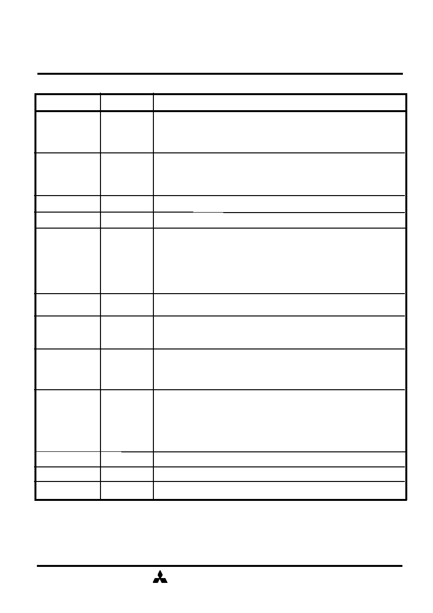
PIN FUNCTION
CLK, /CLK
Input
Clock: CLK and /CLK are differential clock inputs. All address and control
input signals are sampled on the crossing of the positive edge of CLK and
negative edge of /CLK. Output (read) data is referenced to the crossings of
CLK and /CLK (both directions of crossing).
CKE
Input
Clock Enable: CKE controls internal clock. When CKE is low, internal clock
for the following cycle is ceased. CKE is also used to select auto / self refresh.
After self refresh mode is started, CKE becomes asynchronous input. Self refresh
is maintained as long as CKE is low.
/CS
Input
Chip Select: When /CS is high, any command means No Operation.
/RAS, /CAS, /WE
Input
Combination of /RAS, /CAS, /WE defines basic commands.
A0-12
Input
A0-12 specify the Row / Column Address in conjunction with BA0,1. The
Row Address is specified by A0-12. The Column Address is specified by
A0-9,11-12(x4) and A0-9,11(x8). A10 is also used to indicate precharge
option. When A10 is high at a read / write command, an auto precharge is
performed. When A10 is high at a precharge command, all banks are
precharged.
BA0,1
Input
DQ0-7(x8),
DQ0-3(x4)
Input / Output
DQS
Vdd, Vss
Power Supply
Power Supply for the memory array and peripheral circuitry.
VddQ, VssQ
Power Supply
VddQ and VssQ are supplied to the Output Buffers only.
Bank Address: BA0,1 specifies one of four banks to which a command is
applied. BA0,1 must be set with ACT, PRE, READ, WRITE commands.
Data Input/Output: Data bus
Data Strobe: Output pin during Read operation, input during Write operation.
Edge-aligned with read data, placed at the centered of write data to capture
the write data.
SYMBOL
TYPE
DESCRIPTION
DM
Input
Input Data Mask: DM is an input mask signal for write data. Input data
is masked when DM is sampled HIGH along with the input data
during a WRITE operations. DM is sampled on both edges of DQS.
Although DM pins are input only, the DM loading matches the DQ
and DQS loading.
Input / Output
Vref
Input
SSTL_2 reference voltage.
MITSUBISHI
ELECTRIC
-4-
M2S12D20/ 30TP -75, -75L, -10, -10L
Feb. '02
MITSUBISHI LSIs
DDR SDRAM (Rev.1.1)
512M Double Data Rate Synchronous DRAM
MITSUBISHI ELECTRIC
Type Designation Code
This rule is applied to only Synchronous DRAM family.
Mitsubishi Main Designation
Speed Grade 10: 125MHz@CL=2.5,100MHz@CL=2.0
75:
133MHz@CL=2.5
,100MHz@CL=2.0
Package Type TP: TSOP(II)
Process Generation (blank):1st gen.
Function Reserved for Future Use
Organization 2n 2: x4, 3: x8
DDR Synchronous DRAM
Density 12: 512M bits
Interface V:LVTTL, S:SSTL_3, _2
Memory Style (DRAM)
M 2 S 12 D 3 0 TP �75 L
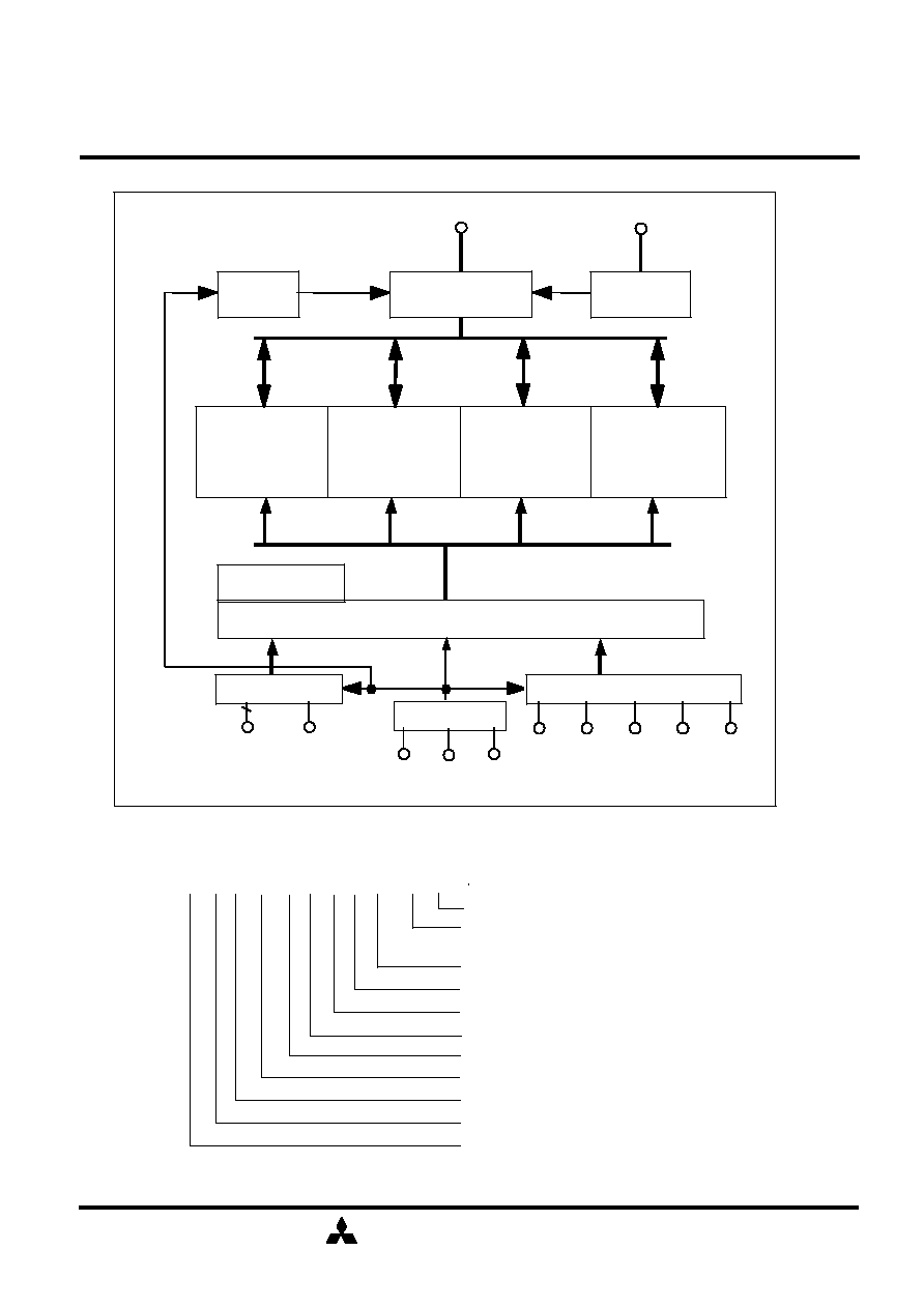
BLOCK DIAGRAM
/CS /RAS /CAS /WE
DM
Memory
Array
Bank #0
DQ0 - 7
I/O Buffer
Memory
Array
Bank #1
Memory
Array
Bank #2
Memory
Array
Bank #3
Mode Register
Control Circuitry
Address Buffer
A0-12
BA0,1
Clock Buffer
CLK
CKE
Control Signal Buffer
QS Buffer
DQS
DLL
/CLK
Power Grade L:Low power, (blank):standard
MITSUBISHI
ELECTRIC
-5-
M2S12D20/ 30TP -75, -75L, -10, -10L
Feb. '02
MITSUBISHI LSIs
DDR SDRAM (Rev.1.1)
512M Double Data Rate Synchronous DRAM
MITSUBISHI ELECTRIC
BASIC FUNCTIONS
The M2S12D20/30TP provides basic functions, bank (row) activate, burst read / write, bank (row)
precharge, and auto / self refresh. Each command is defined by control signals of /RAS, /CAS and
/WE at CLK rising edge. In addition to 3 signals, /CS ,CKE and A10 are used as chip select,
refresh option, and precharge option, respectively. Refer to the command truth table for the
detailed definition of commands.
/CS
Chip Select : L=select, H=deselect
/RAS
Command
/CAS
Command
/WE
Command
CKE
Refresh Option @refresh command
A10
Precharge Option @precharge or read/write command
CLK
define basic commands
/CLK
Activate (ACT) [/RAS =L, /CAS =/WE =H]
ACT command activates one row in an idle bank indicated by BA.
Read (READ) [/RAS =H, /CAS =L, /WE =H]
READ command starts burst read from the active bank indicated by BA. First output data appears after
/CAS latency. When A10 =H in this command, the bank is deactivated after the burst read (auto-
precharge, READA)
Write (WRITE) [/RAS =H, /CAS =/WE =L]
WRITE command starts burst write to the active bank indicated by BA. Total data length to be written
is defined by burst length. When A10 =H in this command, the bank is deactivated after the burst write
(auto-precharge, WRITEA)
Precharge (PRE) [/RAS =L, /CAS =H, /WE =L]
PRE command deactivates the active bank indicated by BA. This command also terminates burst read
/write operation. When A10 =H in this command, all banks are deactivated (precharge all, PREA ).
Auto-Refresh (REFA) [/RAS =/CAS =L, /WE =CKE =H]
REFA command starts auto-refresh cycle. Refresh addresses including bank address are generated
internally. After this command, the banks are precharged automatically.