1
MITSUBISHI ELECTRIC
Mar. '02
MITSUBISHI LSIs
DDR SDRAM
(Rev.1.44)
M2S56D20/ 30/ 40ATP -75AL, -75A, -75L, -75, -10L, -10
256M Double Data Rate Synchronous DRAM
M2S56D20/ 30/ 40AKT -75AL, -75A, -75L, -75, -10L, -10
Contents are subject to change without notice.
DESCRIPTION
M2S56D20ATP / AKT is a 4-bank x 16777216-word x 4-bit,
M2S56D30ATP / AKT is a 4-bank x 8388608-word x 8-bit,
M2S56D40ATP/ AKT is a 4-bank x 4194304-word x 16-bit,
double data rate synchronous DRAM, with SSTL_2 interface. All control and address signals are
referenced to the rising edge of CLK.Input data is registered on both edges of data strobes, and output
data and data strobe are referenced on both edges of CLK. The M2S56D20/30/40ATP achieve very high
speed data rate up to 133MHz, and are suitable for main memory in computer systems.
FEATURES
- VDD=VDDQ=2.5V+0.2V
- Double data rate architecture; two data transfers per clock cycle
- Bidirectional, data strobe (DQS) is transmitted/received with data
- Differential clock inputs (CLK and /CLK)
- DLL aligns DQ and DQS transitions
- Commands are entered on each positive CLK edge
- Data and data mask are referenced to both edges of DQS
- 4-bank operations are controlled by BA0, BA1 (Bank Address)
- /CAS latency- 2.0/2.5 (programmable)
- Burst length- 2/4/8 (programmable)
- Burst type- sequential / interleave (programmable)
- Auto precharge / All bank precharge is controlled by A10
- 8192 refresh cycles /64ms (4 banks concurrent refresh)
- Auto refresh and Self refresh
- Row address A0-12 / Column address A0-9,11(x4)/ A0-9(x8)/ A0-8(x16)
- SSTL_2 Interface
- Both 66-pin TSOP Package and 64-pin Small TSOP Package
M2S56D*0ATP: 0.8mm lead pitch 66-pin TSOP Package
M2S56D*0AKT: 0.4mm lead pitch 64-pin Small TSOP Package
- JEDEC standard
- Low Power for the Self Refresh Current ICC6 : 2mA (-75AL , -75L , -10L)
Operating Frequencies
* CL = CAS(Read) Latency
Standard
DDR200
DDR266B
DDR266A
133MHz
133MHz
100MHz
100MHz
125MHz
133MHz
M2S56D20/30/40ATP/AKT-10L/-10
M2S56D20/30/40ATP/AKT-75L/-75
M2S56D20/30/40ATP/AKT-75AL/-75A
Max. Frequency
@CL=2.5 *
Max. Frequency
@CL=2.0 *

2
MITSUBISHI ELECTRIC
Mar. '02
MITSUBISHI LSIs
DDR SDRAM
(Rev.1.44)
M2S56D20/ 30/ 40ATP -75AL, -75A, -75L, -75, -10L, -10
256M Double Data Rate Synchronous DRAM
M2S56D20/ 30/ 40AKT -75AL, -75A, -75L, -75, -10L, -10
1
2
3
4
5
6
7
8
9
10
11
12
13
14
15
16
17
18
19
20
21
22
23
24
25
26
27
28
29
30
31
32
33
66
65
64
63
62
61
60
59
58
57
56
55
54
53
52
51
50
49
48
47
46
45
44
43
42
41
40
39
38
37
36
35
34
VDD
DQ0
VDDQ
DQ1
DQ2
VSSQ
DQ3
DQ4
VDDQ
DQ5
DQ6
VSSQ
DQ7
NC
VDDQ
LDQS
NC
VDD
NC
LDM
/WE
/CAS
/RAS
/CS
NC
BA0
BA1
A10/AP
A0
A1
A2
A3
VDD
VSS
DQ15
VSSQ
DQ14
DQ13
VDDQ
DQ12
DQ11
VSSQ
DQ10
DQ9
VDDQ
DQ8
NC
VSSQ
UDQS
NC
VREF
VSS
UDM
/CLK
CLK
CKE
NC
A12
A11
A9
A8
A7
A6
A5
A4
VSS
66pin TSOP(II)
400mil width
x
875mil length
0.65mm
Lead Pitch
ROW
A0-12
Column
A0-9,11(x4)
A0-9 (x8)
A0-8 (x16)
VDD
DQ0
VDDQ
NC
DQ1
VSSQ
NC
DQ2
VDDQ
NC
DQ3
VSSQ
NC
NC
VDDQ
NC
NC
VDD
NC
NC
/WE
/CAS
/RAS
/CS
NC
BA0
BA1
A10/AP
A0
A1
A2
A3
VDD
VSS
DQ7
VSSQ
NC
DQ6
VDDQ
NC
DQ5
VSSQ
NC
DQ4
VDDQ
NC
NC
VSSQ
DQS
NC
VREF
VSS
DM
/CLK
CLK
CKE
NC
A12
A11
A9
A8
A7
A6
A5
A4
VSS
VSS
NC
VSSQ
NC
DQ3
VDDQ
NC
NC
VSSQ
NC
DQ2
VDDQ
NC
NC
VSSQ
DQS
NC
VREF
VSS
DM
/CLK
CLK
CKE
NC
A12
A11
A9
A8
A7
A6
A5
A4
VSS
VDD
NC
VDDQ
NC
DQ0
VSSQ
NC
NC
VDDQ
NC
DQ1
VSSQ
NC
NC
VDDQ
NC
NC
VDD
NC
NC
/WE
/CAS
/RAS
/CS
NC
BA0
BA1
A10/AP
A0
A1
A2
A3
VDD
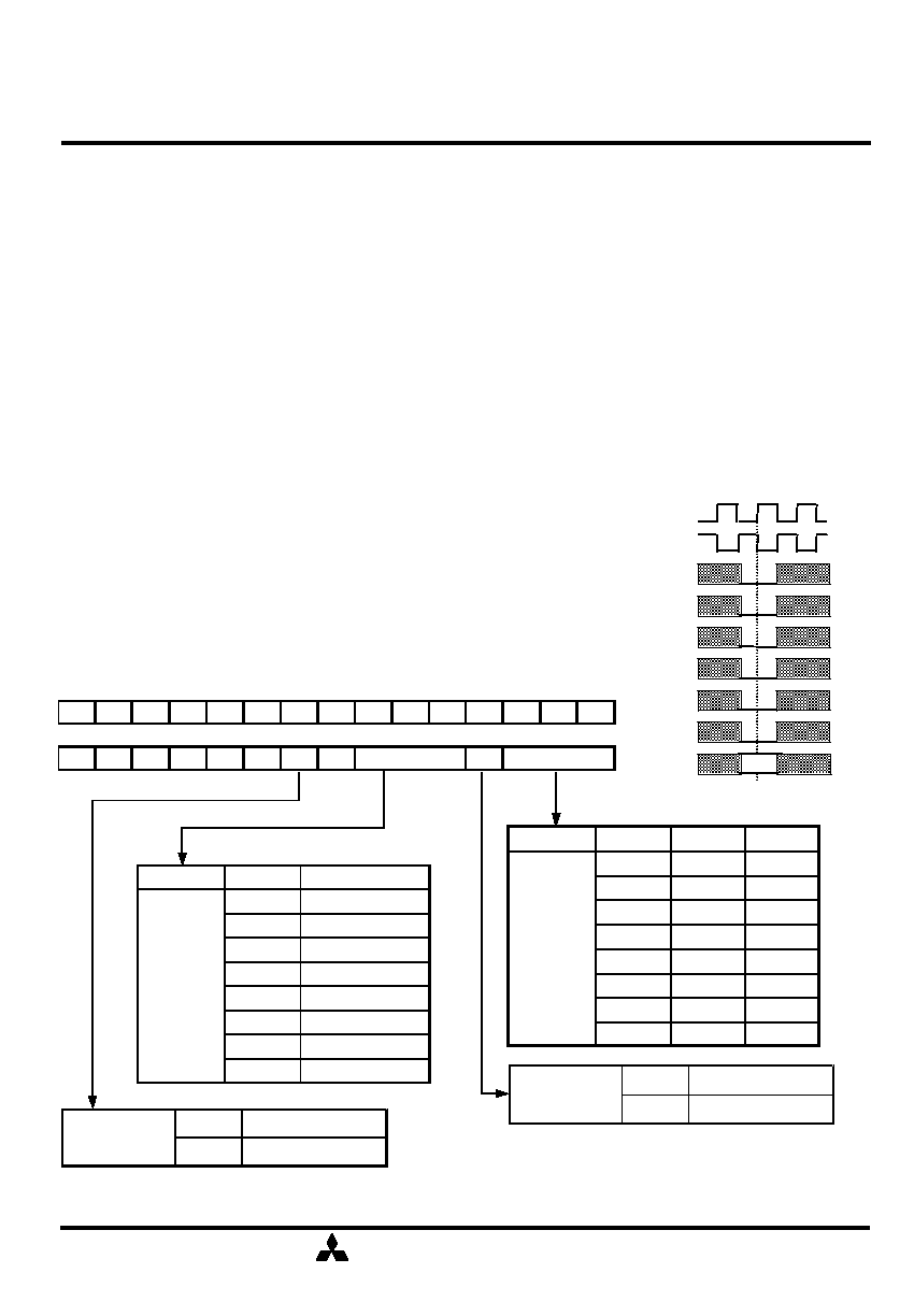
PIN CONFIGURATION(TOP VIEW)
x8
x16
x4
CLK,/CLK
: Master Clock
CKE
: Clock Enable
/CS
: Chip Select
/RAS
: Row Address Strobe
/CAS
: Column Address Strobe
/WE
: Write Enable
DQ0-15
: Data I/O
DQS
LDQS,UDQS
: Data Strobe
DM
LDM,UDM
: Write Mask
VREF
: Reference Voltage
A0-12
: Address Input
BA0,1
: Bank Address Input
VDD
: Power Supply
VDDQ
: Power Supply for Output
VSS
: Ground
VSSQ
: Ground for Output

3
MITSUBISHI ELECTRIC
Mar. '02
MITSUBISHI LSIs
DDR SDRAM
(Rev.1.44)
M2S56D20/ 30/ 40ATP -75AL, -75A, -75L, -75, -10L, -10
256M Double Data Rate Synchronous DRAM
M2S56D20/ 30/ 40AKT -75AL, -75A, -75L, -75, -10L, -10
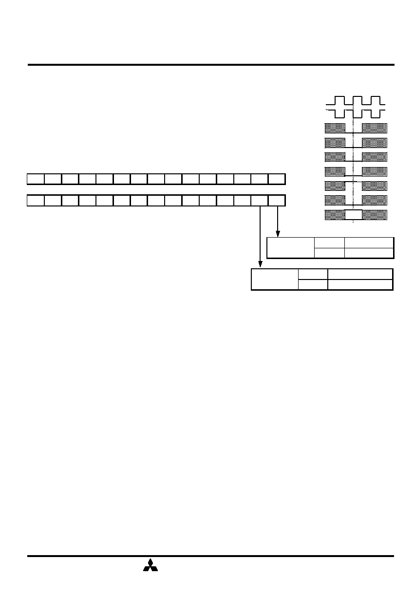
PIN CONFIGURATION(TOP VIEW)
X 8
X 16
X 4
1
2
3
4
5
6
7
8
9
10
11
12
13
14
15
16
17
18
19
20
21
22
23
24
25
26
27
28
29
30
31
32
33
64
63
62
61
60
59
58
57
56
55
54
53
52
51
50
49
48
47
46
45
44
43
42
41
40
39
38
37
36
35
34
64
pin sTSOP
PIN PITCH 0.4 mm
VDD
VDD
VDD
NC
DQ0
DQ0
VDDQ
VDDQ VDDQ
NC
NC
DQ1
DQ0
DQ1
DQ2
VSSQ
VSSQ
VSSQ
NC
NC
DQ3
NC
DQ2
DQ4
VDDQ
VDDQ VDDQ
NC
NC
DQ5
DQ1
DQ3
DQ6
VSSQ
VSSQ
VSSQ
NC
NC
DQ7
NC
NC
LDQS
NC
NC
NC
VDD
VDD
VDD
NC
NC
NC
NC
NC
LDM
/WE
/WE
/WE
/CAS
/CAS
/CAS
/RAS
/RAS
/RAS
/CS
/CS
/CS
NC
NC
NC
BA0
BA0
BA0
BA1
BA1
BA1
A10/AP A10/AP A10/AP
A0
A0
A0
A1
A1
A1
A2
A2
A2
A3
A3
A3
VDD
VDD
VDD
VDDQ
VDDQ VDDQ
VSS
VSS
VSS
DQ15
DQ7
NC
VSSQ VSSQ
VSSQ
DQ14
NC
NC
DQ13
DQ6
DQ3
VDDQ VDDQ VDDQ
DQ12
NC
NC
DQ11
DQ5
NC
VSSQ VSSQ
VSSQ
DQ10
NC
NC
DQ9
DQ4
DQ2
VDDQ VDDQ VDDQ
DQ8
NC
NC
NC
NC
NC
VREF
VREF
VREF
VSS
VSS
VSS
UDM
DM
DM
/CLK
/CLK
/CLK
CLK
CLK
CLK
CKE
CKE
CKE
NC
NC
NC
A12
A12
A12
A11
A11
A11
A9
A9
A9
A8
A8
A8
A7
A7
A7
A6
A6
A6
A5
A5
A5
A4
A4
A4
VSS
VSS
VSS
UDQS
DQS
DQS
VSSQ VSSQ
VSSQ
CLK,/CLK
: Master Clock
CKE
: Clock Enable
/CS
: Chip Select
/RAS
: Row Address Strobe
/CAS
: Column Address Strobe
/WE
: Write Enable
DQ0-15
: Data I/O
DQS
LDQS,UDQS
: Data Strobe
DM
LDM,UDM
: Write Mask
VREF
: Reference Voltage
A0-12
: Address Input
BA0,1
: Bank Address Input
VDD
: Power Supply
VDDQ
: Power Supply for Output
VSS
: Ground
VSSQ
: Ground for Output

4
MITSUBISHI ELECTRIC
Mar. '02
MITSUBISHI LSIs
DDR SDRAM
(Rev.1.44)
M2S56D20/ 30/ 40ATP -75AL, -75A, -75L, -75, -10L, -10
256M Double Data Rate Synchronous DRAM
M2S56D20/ 30/ 40AKT -75AL, -75A, -75L, -75, -10L, -10
Package Outline of sTSOP
33
10.65
+
0.2
9.05
+
0.1
*2
64
32
1
Note)
1. DIMENSIONS "*1" AND "*2"
DO NOT INCLUDE MOLD FLASH.
2. DIMENSION "*3" DOES NOT
INCLUDE TRIM OFFSET.
A
0.125
+0.05
-0.02
1.2 MAX
Detail A (NTS)
0 - 10
0.125+0.075
0.5
+
0.1
(1)
0.8
0.6
+
0.15
0.25
Detail B (NTS)
0.35
0.55 MAX
13.1+0.1
*1
0.4 NOM
0.1
*3
0.16
+0.1
-0.05
B
0.08
M

5
MITSUBISHI ELECTRIC
Mar. '02
MITSUBISHI LSIs
DDR SDRAM
(Rev.1.44)
M2S56D20/ 30/ 40ATP -75AL, -75A, -75L, -75, -10L, -10
256M Double Data Rate Synchronous DRAM
M2S56D20/ 30/ 40AKT -75AL, -75A, -75L, -75, -10L, -10
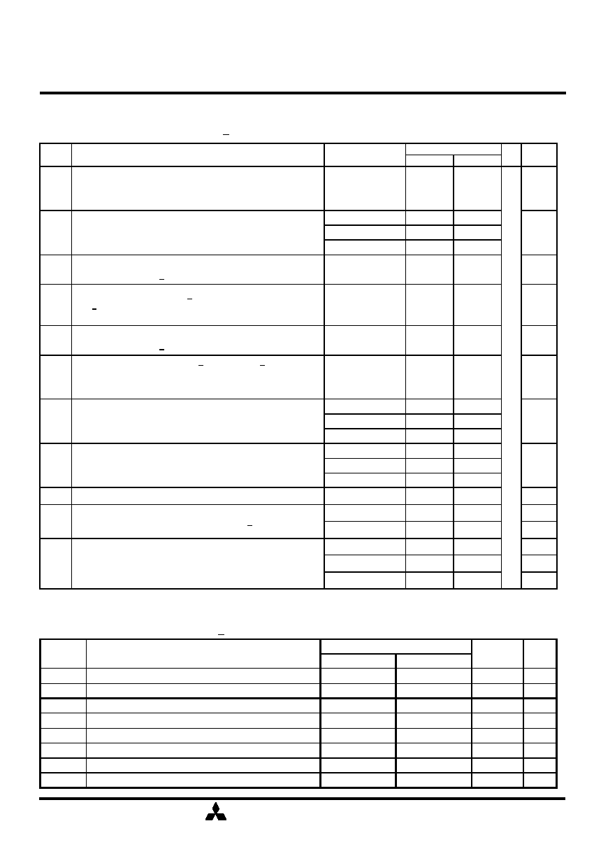
PIN FUNCTION
CLK, /CLK
Input
Clock: CLK and /CLK are differential clock inputs. All address and control
input signals are sampled on the crossing of the positive edge of CLK and
negative edge of /CLK. Output (read) data is referenced to the crossings of
CLK and /CLK (both directions of crossing).
CKE
Input
Clock Enable: CKE controls internal clock. When CKE is low, internal clock
for the following cycle is ceased. CKE is also used to select auto / self
refresh.After self refresh mode is started, CKE becomes asynchronous
input. Self refresh is maintained as long as CKE is low.
/CS
Input
Chip Select: When /CS is high, any command means No Operation.
/RAS, /CAS, /WE
Input
Combination of /RAS, /CAS, /WE defines basic commands.
A0-12
Input
A0-12 specify the Row / Column Address in conjunction with BA0,1. The
Row Address is specified by A0-12. The Column Address is specified by
A0-9,11(x4), A0-9(x8) and A0-8(x16). A10 is also used to indicate precharge
option. When A10 is high at a read / write command, an auto precharge is
performed. When A10 is high at a precharge command, all banks are
precharged.
BA0,1
Input
DQ0-15(x16),
DQ0-7(x8),
DQ0-3(x4),
Input / Output
DQS
VDD, VSS
Power Supply Power Supply for the memory array and peripheral circuitry.
VDDQ, VSSQ
Power Supply VDDQ and VSSQ are supplied to the Output Buffers only.
Bank Address: BA0,1 specifies one of four banks to which a command is
applied. BA0,1 must be set with ACT, PRE, READ, WRITE commands.
Data Input/Output: Data bus
Data Strobe: Output pin during Read operation, input pin during Write
operation. Edge-aligned with read data, placed at the centered of write data
to capture the write data. For the x16, LDQS corresponds to the data on
DQ0-DQ7; UDQS correspond to the data on DQ8-DQ15.
SYMBOL
TYPE
DESCRIPTION
DM
Input
Input Data Mask: DM is an input mask signal for write data. Input data
is masked when DM is sampled HIGH along with the input data
during a WRITE operations. DM is sampled on both edges of DQS.
Although DM pins are input only, the DM loading matches the DQ
and DQS loading. For the x16, LDM corresponds to the data on DQ0-DQ7;
UDM corresponds to the data on DQ8-DQ15.
Input / Output
VREF
Input
SSTL_2 reference voltage.
6
MITSUBISHI ELECTRIC
Mar. '02
MITSUBISHI LSIs
DDR SDRAM
(Rev.1.44)
M2S56D20/ 30/ 40ATP -75AL, -75A, -75L, -75, -10L, -10
256M Double Data Rate Synchronous DRAM
M2S56D20/ 30/ 40AKT -75AL, -75A, -75L, -75, -10L, -10
Type Designation Code
This rule is applied to only Synchronous DRAM family.
Mitsubishi Main Designation
Speed Grade10: 125MHz@CL=2.5,100MHz@CL=2.0
75:
133MHz@CL=2.5
,100MHz@CL=2.0
Package Type TP: TSOP(II), KT: sTSOP(Small TSOP)
Process Generation
Function Reserved for Future Use
Organization 2 n
2: x4, 3: x8, 4: x16
DDR Synchronous DRAM
Density 56: 256M bits
Interface V:LVTTL, S:SSTL_3, _2
Memory Style (DRAM)
M 2 S 56 D 3 0 A KT �75A L
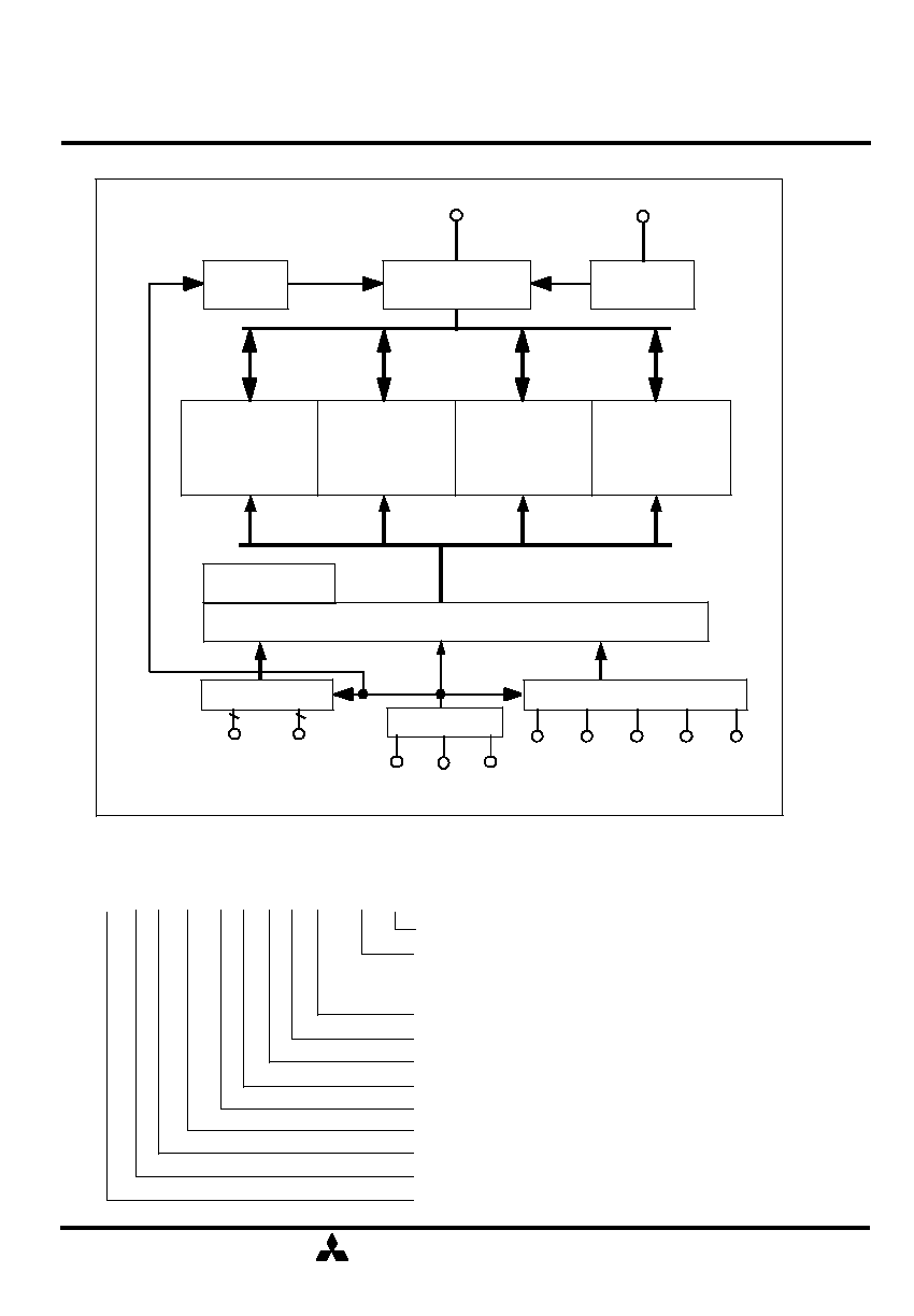
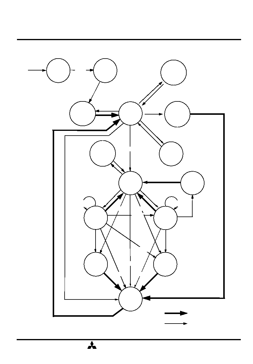
BLOCK DIAGRAM
/CS /RAS /CAS /WE UDM,
LDM
Memory
Array
Bank #0
DQ0 - 15
I/O Buffer
Memory
Array
Bank #1
Memory
Array
Bank #2
Memory
Array
Bank #3
Mode Register
Control Circuitry
Address Buffer
A0-12
BA0,1
Clock Buffer
CLK
CKE
Control Signal Buffer
QS Buffer
UDQS,LDQS
DLL
75A: 133MHz@CL=2.5,
133MHz@CL=2.0
/CLK
(DDR200)
(DDR266B)
(DDR266A)
Power Grade L: Low power, Blank: standard
7
MITSUBISHI ELECTRIC
Mar. '02
MITSUBISHI LSIs
DDR SDRAM
(Rev.1.44)
M2S56D20/ 30/ 40ATP -75AL, -75A, -75L, -75, -10L, -10
256M Double Data Rate Synchronous DRAM
M2S56D20/ 30/ 40AKT -75AL, -75A, -75L, -75, -10L, -10
BASIC FUNCTIONS
The M2S56D20/30/40A* provides basic functions, bank (row) activate, burst read / write, bank (row)
precharge, and auto / self refresh. Each command is defined by control signals of /RAS, /CAS and /WE at
CLK rising edge. In addition to 3 signals, /CS ,CKE and A10 are used as chip select, refresh option, and
precharge option, respectively. Refer to the command truth table for the detailed definition of commands.
/CS
Chip Select : L=select, H=deselect
/RAS
Command
/CAS
Command
/WE
Command
CKE
Refresh Option @refresh command
A10
Precharge Option @precharge or read/write command
CLK
define basic commands
/CLK
Activate (ACT) [/RAS =L, /CAS =/WE =H]
ACT command activates one row in an idle bank indicated by BA.
Read (READ) [/RAS =H, /CAS =L, /WE =H]
READ command starts burst read from the active bank indicated by BA. First output data appears after
/CAS latency. When A10 =H in this command, the bank is deactivated after the burst read (auto-
precharge,
READA)
Write (WRITE) [/RAS =H, /CAS =/WE =L]
WRITE command starts burst write to the active bank indicated by BA. Total data length to be written
is defined by burst length. When A10 =H in this command, the bank is deactivated after the burst write
(auto-precharge,
WRITEA)
Precharge (PRE) [/RAS =L, /CAS =H, /WE =L]
PRE command deactivates the active bank indicated by BA. This command also terminates burst read
/write operation. When A10 =H in this command, all banks are deactivated (precharge all,
PREA ).
Auto-Refresh (REFA) [/RAS =/CAS =L, /WE =CKE =H]
REFA command starts auto-refresh cycle. Refresh addresses including bank address are generated
internally. After this command, the banks are precharged automatically.
8
MITSUBISHI ELECTRIC
Mar. '02
MITSUBISHI LSIs
DDR SDRAM
(Rev.1.44)
M2S56D20/ 30/ 40ATP -75AL, -75A, -75L, -75, -10L, -10
256M Double Data Rate Synchronous DRAM
M2S56D20/ 30/ 40AKT -75AL, -75A, -75L, -75, -10L, -10
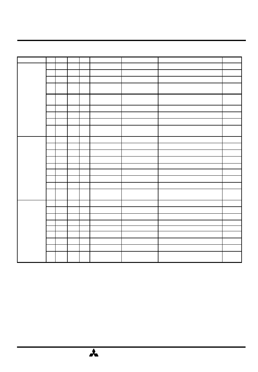
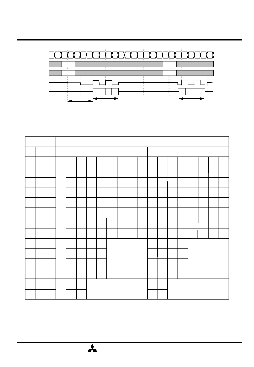
COMMAND TRUTH TABLE
H=High Level, L=Low Level, V=Valid, X=Don't Care, n=CLK cycle number
NOTE:
1. Applies only to read bursts while autoprecharge is disabled; this command is undefined (and should not be
used) during read bursts while autoprecharge is enabled, as well as during write bursts.
2. BA0-BA1 select either the Base or the Extended Mode Register (BA0 = 0, BA1 = 0 selects Mode
Register;BA0=1 ,BA1 = 0 selects Extended Mode Register; other combinations of BA0-BA1 are
reserved; A0-A12 provide the op-codes to be written to the selected Mode Register.
COMMAND
MNEMONIC
CKE
n-1
CKE
n
/CS
/RAS /CAS /WE BA0,1
A10
/AP
A0-9,
11-12
Deselect
DESEL
H
X
H
X
X
X
X
X
X
No Operation
NOP
H
X
L
H
H
H
X
X
X
Row Address Entry &
Bank Activate
ACT
H
H
L
L
H
H
V
V
V
Single Bank Precharge
PRE
H
H
L
L
H
L
V
L
X
Precharge All Banks
PREA
H
H
L
L
H
L
H
X
Column Address Entry
& Write
WRITE
H
H
L
H
L
L
V
L
V
Column Address Entry
& Write with
Auto-Precharge
WRITEA
H
H
L
H
L
L
V
H
V
Column Address Entry
& Read
READ
H
H
L
H
L
H
V
L
V
Column Address Entry
& Read with
Auto-Precharge
READA
H
H
L
H
L
H
V
H
V
Auto-Refresh
REFA
H
H
L
L
L
H
X
X
X
Self-Refresh Entry
REFS
H
L
L
L
L
H
X
X
X
Self-Refresh Exit
REFSX
L
H
H
X
X
X
X
X
X
L
H
L
H
H
H
X
X
X
Burst Terminate
TERM
H
H
L
H
H
L
X
X
X
Mode Register Set
MRS
H
H
L
L
L
L
L
L
V
X
note
1
2

9
MITSUBISHI ELECTRIC
Mar. '02
MITSUBISHI LSIs
DDR SDRAM
(Rev.1.44)
M2S56D20/ 30/ 40ATP -75AL, -75A, -75L, -75, -10L, -10
256M Double Data Rate Synchronous DRAM
M2S56D20/ 30/ 40AKT -75AL, -75A, -75L, -75, -10L, -10
FUNCTION TRUTH TABLE
Current State /CS /RAS /CAS /WE Address
Command
Action
Notes
IDLE
H
X
X
X X
DESEL
NOP
L
H
H
H X
NOP
NOP
L
H
H
L BA
TERM
ILLEGAL
2
L
H
L
X BA, CA, A10
READ / WRITE
ILLEGAL
2
L
L
H
H BA, RA
ACT
Bank Active, Latch RA
L
L
H
L BA, A10
PRE / PREA
NOP
4
L
L
L
H X
REFA
Auto-Refresh
5
L
L
L
L
Op-Code,
Mode-Add
MRS
Mode Register Set
5
ROW ACTIVE H
X
X
X X
DESEL
NOP
L
H
H
H X
NOP
NOP
L
H
H
L BA
TERM
NOP
L
H
L
H BA, CA, A10
READ / READA
Begin Read, Latch CA,
Determine Auto-Precharge
L
H
L
L BA, CA, A10
WRITE / WRITEA
Begin Write, Latch CA,
Determine Auto-Precharge
L
L
H
H BA, RA
ACT
Bank Active / ILLEGAL
2
L
L
H
L BA, A10
PRE / PREA
Precharge / Precharge All
L
L
L
H X
REFA
ILLEGAL
L
L
L
L
Op-Code,
Mode-Add
MRS
ILLEGAL
H
X
X
X X
DESEL
NOP (Continue Burst to END)
L
H
H
H X
NOP
NOP (Continue Burst to END)
L
H
H
L BA
TERM
Terminate Burst
L
H
L
H BA, CA, A10
READ / READA
Terminate Burst, Latch CA, Begin
New Read, Determine Auto-
Precharge
3
L
H
L
L BA, CA, A10
WRITE / WRITEA ILLEGAL
L
L
H
H BA, RA
ACT
Bank Active / ILLEGAL
2
L
L
H
L BA, A10
PRE / PREA
Terminate Burst, Precharge
L
L
L
H X
REFA
ILLEGAL
L
L
L
L
Op-Code,
Mode-Add
MRS
ILLEGAL
READ(Auto-
Precharge
Disabled)
10
MITSUBISHI ELECTRIC
Mar. '02
MITSUBISHI LSIs
DDR SDRAM
(Rev.1.44)
M2S56D20/ 30/ 40ATP -75AL, -75A, -75L, -75, -10L, -10
256M Double Data Rate Synchronous DRAM
M2S56D20/ 30/ 40AKT -75AL, -75A, -75L, -75, -10L, -10
FUNCTION TRUTH TABLE (continued)
Current State /CS /RAS /CAS /WE Address
Command
Action
Notes
H
X
X
X X
DESEL
NOP (Continue Burst to END)
L
H
H
H X
NOP
NOP (Continue Burst to END)
L
H
H
L BA
TERM
ILLEGAL
L
H
L
H BA, CA, A10
READ / READA
Terminate Burst, Latch CA, Begin
Read, Determine Auto-Precharge
3
L
H
L
L BA, CA, A10
WRITE / WRITEA
Terminate Burst, Latch CA, Begin
Write, Determine Auto-Precharge
3
L
L
H
H BA, RA
ACT
Bank Active / ILLEGAL
2
L
L
H
L BA, A10
PRE / PREA
Terminate Burst, Precharge
L
L
L
H X
REFA
ILLEGAL
L
L
L
L
Op-Code,
Mode-Add
MRS
ILLEGAL
H
X
X
X X
DESEL
NOP (Continue Burst to END)
L
H
H
H X
NOP
NOP (Continue Burst to END)
L
H
H
L BA
TERM
ILLEGAL
L
H
L
H BA, CA, A10
READ / READA
ILLEGAL for Same Bank
6
L
H
L
L BA, CA, A10
WRITE / WRITEA ILLEGAL for Same Bank
6
L
L
H
H BA, RA
ACT
Bank Active / ILLEGAL
2
L
L
H
L BA, A10
PRE / PREA
Precharge / ILLEGAL
2
L
L
L
H X
REFA
ILLEGAL
L
L
L
L
Op-Code,
Mode-Add
MRS
ILLEGAL
H
X
X
X X
DESEL
NOP (Continue Burst to END)
L
H
H
H X
NOP
NOP (Continue Burst to END)
L
H
H
L BA
TERM
ILLEGAL
L
H
L
H BA, CA, A10
READ / READA
ILLEGAL for Same Bank
7
L
H
L
L BA, CA, A10
WRITE / WRITEA ILLEGAL for Same Bank
7
L
L
H
H BA, RA
ACT
Bank Active / ILLEGAL
2
L
L
H
L BA, A10
PRE / PREA
Precharge / ILLEGAL
2
L
L
L
H X
REFA
ILLEGAL
L
L
L
L
Op-Code,
Mode-Add
MRS
ILLEGAL
WRITE(Auto-
Precharge
Disabled)
READ with
Auto-
Precharge
WRITE with
Auto-
Precharge
11
MITSUBISHI ELECTRIC
Mar. '02
MITSUBISHI LSIs
DDR SDRAM
(Rev.1.44)
M2S56D20/ 30/ 40ATP -75AL, -75A, -75L, -75, -10L, -10
256M Double Data Rate Synchronous DRAM
M2S56D20/ 30/ 40AKT -75AL, -75A, -75L, -75, -10L, -10
FUNCTION TRUTH TABLE (continued)
Current State /CS /RAS /CAS /WE Address
Command
Action
Notes
H
X
X
X X
DESEL
NOP (Idle after tRP)
L
H
H
H X
NOP
NOP (Idle after tRP)
L
H
H
L BA
TERM
ILLEGAL
2
L
H
L
X BA, CA, A10
READ / WRITE
ILLEGAL
2
L
L
H
H BA, RA
ACT
ILLEGAL
2
L
L
H
L BA, A10
PRE / PREA
NOP (Idle after tRP)
4
L
L
L
H X
REFA
ILLEGAL
L
L
L
L
Op-Code,
Mode-Add
MRS
ILLEGAL
H
X
X
X X
DESEL
NOP (Row Active after tRCD)
L
H
H
H X
NOP
NOP (Row Active after tRCD)
L
H
H
L BA
TERM
ILLEGAL
2
L
H
L
X BA, CA, A10
READ / WRITE
ILLEGAL
2
L
L
H
H BA, RA
ACT
ILLEGAL
2
L
L
H
L BA, A10
PRE / PREA
ILLEGAL
2
L
L
L
H X
REFA
ILLEGAL
L
L
L
L
Op-Code,
Mode-Add
MRS
ILLEGAL
H
X
X
X X
DESEL
NOP
L
H
H
H X
NOP
NOP
L
H
H
L BA
TERM
ILLEGAL
2
L
H
L
X BA, CA, A10
READ / WRITE
ILLEGAL
2
L
L
H
H BA, RA
ACT
ILLEGAL
2
L
L
H
L BA, A10
PRE / PREA
ILLEGAL
2
L
L
L
H X
REFA
ILLEGAL
L
L
L
L
Op-Code,
Mode-Add
MRS
ILLEGAL
ROW
ACTIVATING
WRITE RE-
COVERING
PRE-
CHARGING
12
MITSUBISHI ELECTRIC
Mar. '02
MITSUBISHI LSIs
DDR SDRAM
(Rev.1.44)
M2S56D20/ 30/ 40ATP -75AL, -75A, -75L, -75, -10L, -10
256M Double Data Rate Synchronous DRAM
M2S56D20/ 30/ 40AKT -75AL, -75A, -75L, -75, -10L, -10
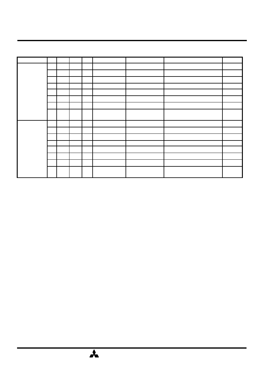
FUNCTION TRUTH TABLE (continued)
ABBREVIATIONS:
H=High Level, L=Low Level, X=Don't Care
BA=Bank Address, RA=Row Address, CA=Column Address, NOP=No Operation
NOTES:
1. All entries are valid only when CKE was High during the preceding clock cycle and the current clock cycle.
2. ILLEGAL to bank in specified state; function may be legal in the bank indicated by BA, depending on the
state of specific bank.
3. Must satisfy bus contention, bus turn around, write recovery requirements.
4. NOP to bank precharging or in idle state. May precharge bank indicated by BA.
5. ILLEGAL if any bank is not idle.
6. Refer to Read with Auto-Precharge in page 27.
7. Refer to Write with Auto-Precharge in page 29.
ILLEGAL = Device operation and/or data-integrity are not guaranteed.
Current State /CS /RAS /CAS /WE Address
Command
Action
Notes
REFRESHING H
X
X
X X
DESEL
NOP (Idle after tRFC)
L
H
H
H X
NOP
NOP (Idle after tRFC)
L
H
H
L
BA
TERM
ILLEGAL
L
H
L
X BA, CA, A10
READ / WRITE
ILLEGAL
L
L
H
H BA, RA
ACT
ILLEGAL
L
L
H
L
BA, A10
PRE / PREA
ILLEGAL
L
L
L
H X
REFA
ILLEGAL
L
L
L
L
Op-Code,
Mode-Add
MRS
ILLEGAL
H
X
X
X X
DESEL
NOP (Idle after tMRD)
L
H
H
H X
NOP
NOP (Idle after tMRD)
L
H
H
L
BA
TERM
ILLEGAL
L
H
L
X BA, CA, A10
READ / WRITE
ILLEGAL
L
L
H
H BA, RA
ACT
ILLEGAL
L
L
H
L
BA, A10
PRE / PREA
ILLEGAL
L
L
L
H X
REFA
ILLEGAL
L
L
L
L
Op-Code,
Mode-Add
MRS
ILLEGAL
MODE
REGISTER
SETTING

13
MITSUBISHI ELECTRIC
Mar. '02
MITSUBISHI LSIs
DDR SDRAM
(Rev.1.44)
M2S56D20/ 30/ 40ATP -75AL, -75A, -75L, -75, -10L, -10
256M Double Data Rate Synchronous DRAM
M2S56D20/ 30/ 40AKT -75AL, -75A, -75L, -75, -10L, -10
FUNCTION TRUTH TABLE for CKE
ABBREVIATIONS:
H=High Level, L=Low Level, X=Don't Care
NOTES:
1. Low to High transition of CKE re-enable CLK and other inputs asynchronously.
A minimum setup time must be satisfied before any command except REFSX.
2. Power-Down and Self-Refresh can be entered only from the All Banks Idle State.
3. Must be legal command.
Current State CKE n-1 CKE n
/CS
/RAS
/CAS
/WE Address
Action
Notes
H
X
X
X
X
X
X
INVALID
1
L
H
H
X
X
X
X
Exit Self-Refresh (Idle after tRFC)
1
L
H
L
H
H
H
X
Exit Self-Refresh (Idle after tRFC)
1
L
H
L
H
H
L
X
ILLEGAL
1
L
H
L
H
L
X
X
ILLEGAL
1
L
H
L
L
X
X
X
ILLEGAL
1
L
L
X
X
X
X
X
NOP (Maintain Self-Refresh)
1
H
X
X
X
X
X
X
INVALID
L
H
X
X
X
X
X
Exit Power Down to Idle
L
L
X
X
X
X
X
NOP (Maintain Power Down)
H
H
X
X
X
X
X
Refer to Function Truth Table
2
H
L
L
L
L
H
X
Enter Self-Refresh
2
H
L
H
X
X
X
X
Enter Power Down
2
H
L
L
H
H
H
X
Enter Power Down
2
H
L
L
H
H
L
X
ILLEGAL
2
H
L
L
H
L
X
X
ILLEGAL
2
H
L
L
L
X
X
X
ILLEGAL
2
L
X
X
X
X
X
X
Refer to Current State =Power
Down
2
H
H
X
X
X
X
X
Refer to Function Truth Table
H
L
X
X
X
X
X
Begin CLK Suspend at Next
Cycle
3
L
H
X
X
X
X
X
Exit CLK Suspend at Next Cycle
3
L
L
X
X
X
X
X
Maintain CLK Suspend
ANY STATE
other than
listed above
SELF-
REFRESHING
POWER
DOWN
ALL BANKS
IDLE
14
MITSUBISHI ELECTRIC
Mar. '02
MITSUBISHI LSIs
DDR SDRAM
(Rev.1.44)
M2S56D20/ 30/ 40ATP -75AL, -75A, -75L, -75, -10L, -10
256M Double Data Rate Synchronous DRAM
M2S56D20/ 30/ 40AKT -75AL, -75A, -75L, -75, -10L, -10
SIMPLIFIED STATE DIAGRAM
ROW
ACTIVE
IDLE
PRE
CHARGE
POWER
DOWN
READ
READA
WRITE
WRITEA
POWER
ON
ACT
REFA
REFS
REFSX
CKEL
CKEH
MRS / EMRS
CKEL
CKEH
WRITE
READ
WRITEA
WRITEA
READA
READ
PRE
READA
READA
PRE
PRE
PREA
POWER
APPLIED
MODE
REGISTER
SET
SELF
REFRESH
AUTO
REFRESH
Active
Power
Down
Automatic Sequence
Command Sequence
WRITE
READ
PRE
CHARGE
ALL
MRS / EMRS
BURST
STOP
TERM
15
MITSUBISHI ELECTRIC
Mar. '02
MITSUBISHI LSIs
DDR SDRAM
(Rev.1.44)
M2S56D20/ 30/ 40ATP -75AL, -75A, -75L, -75, -10L, -10
256M Double Data Rate Synchronous DRAM
M2S56D20/ 30/ 40AKT -75AL, -75A, -75L, -75, -10L, -10
POWER ON SEQUENCE
The following power on sequences are necessary to guarantee the proper operations of the
DDR SDRAM.
1. Apply VDD before or at the same time as VDDQ
2. Apply VDDQ before or at the same time as VTT & VREF
3. Maintain stable conditions for 200us after stable power and CLK are applied, assert NOP or DSEL
4. Issue Precharge command for all banks of the device
5. Issue EMRS to program proper functions
6. Issue MRS to configure the Mode Register and to reset the DLL
7. Issue 2 or more Auto Refresh commands
8. Maintain stable conditions for 200 cycle
After these sequences, the DDR SDRAM is in the idle state and ready for normal operation.
MODE REGISTER
Burst Length, Burst Type and /CAS Latency can be programmed by
configuring the mode register (MRS). The mode register stores these data
until the next MRS command, which may be issued when both banks are in
idle state. After tMRD from an MRS command, the DDR SDRAM is ready to
accept the new command.
/CS
/RAS
/CAS
/WE
A11-A0
/CLK
CLK
BA0
BA1
R: Reserved for Future Use
0
NO
1
YES
DLL Reset
0
Sequential
1
Interleaved
Burst Type
BT=0
BT=1
0 0 0
R
R
0 0 1
2
2
0 1 0
4
4
0 1 1
8
8
1 0 0
R
R
1 0 1
R
R
1 1 0
R
R
1 1 1
R
R
BL
Burst
Length
/CAS Latency
0 0 0
R
0 0 1
R
0 1 0
2
0 1 1
R
1 0 0
R
1 0 1
R
1 1 0
2.5
1 1 1
R
CL
Latency
Mode
BA1 BA0 A12 A11 A10 A9 A8 A7 A6 A5 A4 A3 A2 A1 A0
0
0
0
0
0
0
DR
0
BT
LTMODE
BL
V
16
MITSUBISHI ELECTRIC
Mar. '02
MITSUBISHI LSIs
DDR SDRAM
(Rev.1.44)
M2S56D20/ 30/ 40ATP -75AL, -75A, -75L, -75, -10L, -10
256M Double Data Rate Synchronous DRAM
M2S56D20/ 30/ 40AKT -75AL, -75A, -75L, -75, -10L, -10
EXTENDED MODE REGISTER
DLL disable / enable mode can be programmed in the extended
mode register (EMRS). The extended mode register stores these
data until the next EMRS command, which may be issued when all
banks are in idle state. After tMRD from a EMRS command, the DDR
SDRAM is ready to accept the new command.
/CS
/RAS
/CAS
/WE
A11-A0
BA0
BA1
/CLK
CLK
BA1 BA0 A12 A11 A10 A9 A8 A7 A6 A5 A4 A3 A2 A1 A0
0
1
0
0
0
0
0
0
0
0
0
0
0
DS DD
0
Normal
1
Weak (Optional)
Drive
Strength
0
DLL Enable
1
DLL Disable
DLL Disable
V
17
MITSUBISHI ELECTRIC
Mar. '02
MITSUBISHI LSIs
DDR SDRAM
(Rev.1.44)
M2S56D20/ 30/ 40ATP -75AL, -75A, -75L, -75, -10L, -10
256M Double Data Rate Synchronous DRAM
M2S56D20/ 30/ 40AKT -75AL, -75A, -75L, -75, -10L, -10
/CAS
Latency
Burst
Length
CL= 2
BL= 4
Burst
Length
A2 A1 A0
Initial Address BL
Sequential
Interleaved
Column Addressing
0
0
0
0
0
1
0
1
0
0
1
1
1
0
0
1
0
1
1
1
0
1
1
1
-
0
0
-
0
1
-
1
0
-
1
1
-
-
0
0
1
2
3
4
5
6
7
0
1
2
3
4
5
6
7
1
2
3
4
5
6
7
0
1
0
3
2
5
4
7
6
2
3
4
5
6
7
0
1
2
3
0
1
6
7
4
5
3
4
5
6
7
0
1
2
3
2
1
0
7
6
5
4
4
5
6
7
0
1
2
3
4
5
6
7
0
1
2
3
5
6
7
0
1
2
3
4
5
4
7
6
1
0
3
2
6
7
0
1
2
3
4
5
6
7
4
5
2
3
0
1
7
0
1
2
0
1
2
3
1
2
3
0
2
3
0
1
3
0
0
1
7
6
5
4
0
1
2
3
1
0
3
2
2
3
0
1
3
2
0
1
-
-
1
1
2
1
0
3
4
5
6
3
2
1
0
1
0
1
0
8
4
2
Command
Address
DQ
Y
Y
Read
Write
DQS
Q0 Q1 Q2 Q3
D0 D1 D2 D3
/CLK
CLK
18
MITSUBISHI ELECTRIC
Mar. '02
MITSUBISHI LSIs
DDR SDRAM
(Rev.1.44)
M2S56D20/ 30/ 40ATP -75AL, -75A, -75L, -75, -10L, -10
256M Double Data Rate Synchronous DRAM
M2S56D20/ 30/ 40AKT -75AL, -75A, -75L, -75, -10L, -10
ABSOLUTE MAXIMUM RATINGS
DC OPERATING CONDITIONS
(Ta=0 ~ 70
o
C, unless otherwise noted)
Min.
Typ.
Max.
VDD
Supply Voltage
2.3
2.5
2.7
V
VDDQ
Supply Voltage for Output
2.3
2.5
2.7
V
VREF
Input Reference Voltage
0.49*VDDQ 0.50*VDDQ 0.51*VDDQ
V
5
VIH(DC)
High-Level Input Voltage
VREF + 0.15
VDDQ+0.3
V
VIL(DC)
Low-Level Input Voltage
-0.3
VREF - 0.15
V
VIN(DC)
Input Voltage Level, CLK and /CLK
-0.3
VDDQ + 0.3
V
VID(DC) Input Differential Voltage, CLK and /CLK
0.36
VDDQ + 0.6
V
7
VTT
I/O Termination Voltage
VREF - 0.04
VREF + 0.04
V
6
Notes
Limits
Symbol
Parameter
Unit
Symbol
Parameter
Conditions
Ratings
Unit
VDD
Supply Voltage
with respect to VSS
-0.5 ~ 3.7
V
VDDQ
Supply Voltage for Output
with respect to VSSQ
-0.5 ~ 3.7
V
VI
Input Voltage
with respect to VSS
-0.5 ~ VDD+0.5
V
VO
Output Voltage
with respect to VSSQ
-0.5 ~ VDDQ+0.5
V
IO
Output Current
50
mA
Pd
Power Dissipation
Ta = 25
o
C
1000
mW
Topr
Operating Temperature
0 ~ 70
o
C
Tstg
Storage Temperature
-65 ~ 150
o
C
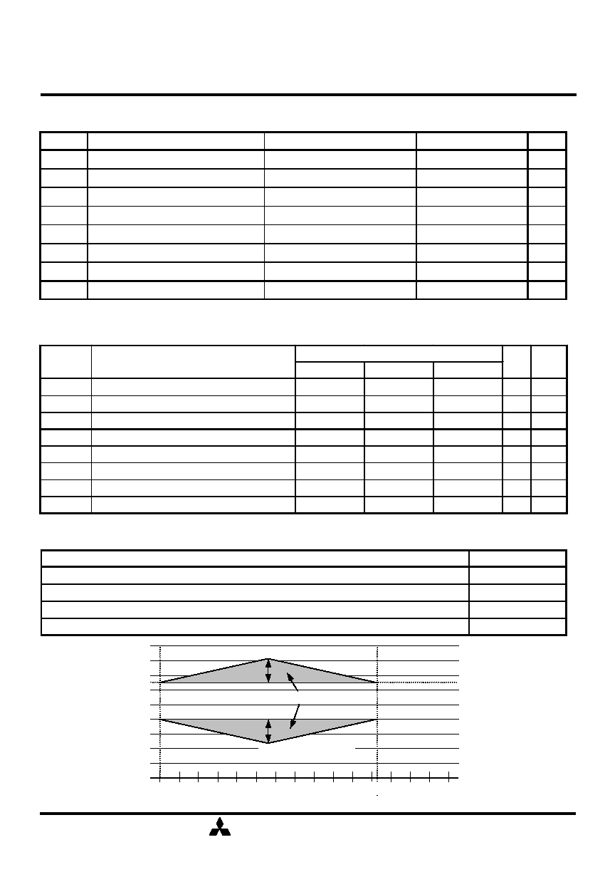
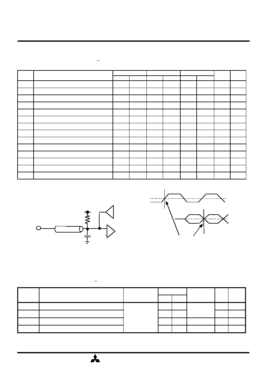
AC OVERSHOOT/UNDERSHOOT SPECIFICATION
Parameter
Specification
Maximum peak amplitude allowed for overshoot
1.6V
Maximum peak amplitude allowed for undershoot
1.6V
The area between the overshoot signal and VDD must be less than or euqal to
4.5 V-ns
The area between the undershoot signal and VSS must be less than or euqal to
4.5 V-ns
Volts (V)
5
4
3
2
1
VSS(0)
-1
-2
-3
0 0.5 1 1.5 2 2.5 3 3.5 4 4.5 5 5.5 6 6.5 7 7.5
5.625
Maximum Amplitude
Overshoot
Undershoot
Maximum Amplitude
Area (max.4.5V-ns)
VDD
Time (ns)
19
MITSUBISHI ELECTRIC
Mar. '02
MITSUBISHI LSIs
DDR SDRAM
(Rev.1.44)
M2S56D20/ 30/ 40ATP -75AL, -75A, -75L, -75, -10L, -10
256M Double Data Rate Synchronous DRAM
M2S56D20/ 30/ 40AKT -75AL, -75A, -75L, -75, -10L, -10
-75A / -75
-10
x4
95
85
x8
100
90
x16
115
105
x4
140
100
x8
150
115
x16
180
145
x4
130
95
x8
140
105
x16
160
120
IDD5 AUTO REFRESH CURRENT: t RC = t RFC (MIN)
ALL
140
130
ALL(-75A/-75/-10)
3
3
9
ALL(-75AL/-75A/-10L)
2
2
9,21
x4
215
170
20
x8
235
185
20
x16
270
210
20
IDD6
SELF REFRESH CURRENT: CKE < 0.2V
6
6
ALL
IDD4W
OPERATING CURRENT: Burst = 2; Writes; Continuous burst; One bank
active; Address and control inputs changing once per clock cycle;
CL=2.5; t CK = t CK MIN;DQ, DM and DQS inputs changing twice per
clock cycle
ALL
ALL
IDD3P
ACTIVE POWER-DOWN STANDBY CURRENT: One bank active;
power-down mode; CKE < VIL (MAX); t CK = t CK MIN
ACTIVE STANDBY CURRENT: /CS > VIH (MIN); CKE > VIH (MIN); One
bank; Active-Precharge; t RC = t RAS MAX; t CK = t CK MIN; DQ,DM
and DQS inputs changing twice per clock cycle; address and other
control inputs changing once per clock cycle
IDD3N
ALL
45
IDD7
OPERATING CURRENT-Four bank Operation: Four bank are interleaved
with BL=4, refer to the Notes 20
35
IDD4R
OPERATING CURRENT: Burst = 2; Reads; Continuous burst;One bank
active; Address and control inputs changing once per clock cycle;CL=2.5;
t CK = t CK MIN; IOUT = 0 mA
mA
PRECHARGE POWER-DOWN STANDBY CURRENT: All banks idle;
power-down mode; CKE <VIL (MAX); t CK = t CK MIN
25
30
15
12
Organization
Parameter/Test Conditions
OPERATING CURRENT: One Bank; Active-Precharge; t RC = t RC MIN;
t CK = t CK MIN; DQ, DM and DQS inputs changing twice per clock
cycle; address and control inputs changing once per clock cycle
Unit
Limits(Max.)
ALL
85
75
IDD2P
IDD2F
IDLE STANDBY CURRENT: /CS > VIH (MIN); All banks idle;
CKE > VIH (MIN); t CK = t CK MIN; Address and other control inputs
changing once per clock cycle
Notes
IDD0
IDD1
OPERATING CURRENT: One Bank; Active-Read-Precharge;
Burst = 2; t RC = t RC MIN; CL = 2.5; t CK = t CK MIN; IOUT= 0mA;
Address and control inputs changing once per clock cycle
Symbol
AVERAGE SUPPLY CURRENT from VDD
(Ta=0 ~ 70
o
C, VDD = VDDQ = 2.5V + 0.2V, VSS = VSSQ = 0V, Output Open, unless otherwise noted)
AC OPERATING CONDITIONS AND CHARACTERISTICS
(Ta=0 ~ 70
o
C, VDD = VDDQ = 2.5V + 0.2V, VSS = VSSQ = 0V, Output Open, unless otherwise noted)
Min.
Max.
VIH(AC) High-Level Input Voltage (AC)
VREF + 0.31
VIL(AC) Low-Level Input Voltage (AC)
VREF - 0.31
VID(AC) Input Differential Voltage, CLK and /CLK
0.7
VDDQ + 0.6
7
VIX(AC) Input Crossing Point Voltage, CLK and /CLK
0.5*VDDQ - 0.2 0.5*VddQ + 0.2
8
IOZ
Off-state Output Current /Q floating Vo=0~VddQ
-5
5
II
Input Current / VIN=0 ~ VddQ
-2
2
IOH
Output High Current (VOUT = VTT+0.84V)
-16.8
IOL
Output High Current (VOUT = VTT-0.84V)
16.8
Symbol
Parameter / Test Conditions
Unit
V
mA
mA
Notes
Limits
V
V
V
mA
mA

20
MITSUBISHI ELECTRIC
Mar. '02
MITSUBISHI LSIs
DDR SDRAM
(Rev.1.44)
M2S56D20/ 30/ 40ATP -75AL, -75A, -75L, -75, -10L, -10
256M Double Data Rate Synchronous DRAM
M2S56D20/ 30/ 40AKT -75AL, -75A, -75L, -75, -10L, -10
AC TIMING REQUIREMENTS
(Ta=0 ~ 70
o
C, VDD = VDDQ = 2.5V +0.2V, VSS = VSSQ = 0V, unless otherwise noted)
Min.
Max
Min.
Max
Min.
Max
tAC
DQ Output Valid data delay time from CLK//CLK
-0.75
0.75
-0.75
0.75
-0.8
0.8
ns
tDQSCK DQ Output Valid data delay time from CLK//CLK
-0.75
0.75
-0.75
0.75
-0.8
0.8
ns
tCH
CLK High level width
0.45
0.55
0.45
0.55
0.45
0.55
tCK
tCL
CLK Low level width
0.45
0.55
0.45
0.55
0.45
0.55
tCK
CL=2.5
7.5
15
7.5
15
8
15
ns
CL=2
7.5
15
10
15
10
15
ns
tDS
Input Setup time (DQ,DM)
0.5
0.5
0.6
ns
tDH
Input Hold time(DQ,DM)
0.5
0.5
0.6
ns
tDIPW DQ and DM input pulse width (for each input)
1.75
1.75
2
ns
tHZ
Data-out-high impedance time from CLK//CLK
-0.75
0.75
-0.75
0.75
-0.8
0.8
ns
14
tLZ
Data-out-low impedance time from CLK//CLK
-0.75
0.75
-0.75
0.75
-0.8
0.8
ns
14
tDQSQ DQ Valid data delay time from DQS
0.5
0.5
0.6
ns
tHP
Clock half period
tCLmin
or
tCHmin
tCLmin
or
tCHmin
tCLmin
or
tCHmin
ns
tQH
Output DQS valid window
tHP-0.75
tHP-0.75
tHP-1.0
ns
tDQSS Write command to first DQS latching transition
0.75
1.25
0.75
1.25
0.75
1.25
tCK
tDQSH DQS input High level width
0.35
0.35
0.35
tCK
tDQSL DQS input Low level width
0.35
0.35
0.35
tCK
tDSS
DQS falling edge to CLK setup time
0.2
0.2
0.2
tCK
tDSH
DQS falling edge hold time from CLK
0.2
0.2
0.2
tCK
tMRD
Mode Register Set command cycle time
15
15
15
ns
tWPRES Write preamble setup time
0
0
0
ns
16
tWPST Write postamble
0.4
0.6
0.4
0.6
0.4
0.6
tCK
15
tWPRE Write preamble
0.25
0.25
0.25
tCK
tIS
Input Setup time (address and control)
0.9
0.9
1.1
ns
19
tIH
Input Hold time (address and control)
0.9
0.9
1.1
ns
19
tRPST Read postamble
0.4
0.6
0.4
0.6
0.4
0.6
tCK
tRPRE Read preamble
0.9
1.1
0.9
1.1
0.9
1.1
tCK
-10
Unit Notes
tCK
CLK cycle time
Symbol
AC Characteristics Parameter
-75A
-75
21
MITSUBISHI ELECTRIC
Mar. '02
MITSUBISHI LSIs
DDR SDRAM
(Rev.1.44)
M2S56D20/ 30/ 40ATP -75AL, -75A, -75L, -75, -10L, -10
256M Double Data Rate Synchronous DRAM
M2S56D20/ 30/ 40AKT -75AL, -75A, -75L, -75, -10L, -10
AC TIMING REQUIREMENTS(Continued)
(Ta=0 ~ 70
o
C, VDD = VDDQ = 2.5V +0.2V, VSS = VSSQ = 0V, unless otherwise noted)
Min.
Max
Min.
Max
Min.
Max
tRAS
Row Active time
45
120,000
45
120,000
50
120,000
ns
tRC
Row Cycle time(operation)
65
65
70
ns
tRFC
Auto Ref. to Active/Auto Ref. command period
75
75
80
ns
tRCD
Row to Column Delay
20
20
20
ns
tRP
Row Precharge time
20
20
20
ns
tRRD
Act to Act Delay time
15
15
15
ns
tWR
Write Recovery time
15
15
15
ns
tDAL
Auto Precharge write recovery + precharge time
35
35
35
ns
tWTR
Internal Write to Read Command Delay
1
1
1
tCK
tXSNR Exit Self Ref. to non-Read command
75
75
80
ns
tXSRD Exit Self Ref. to -Read command
200
200
200
tCK
tXPNR Exit Power down to command
1
1
1
tCK
tXPRD Exit Power down to -Read command
1
1
1
tCK
18
tREFI Average Periodic Refresh interval
7.8
7.8
7.8
us
17
-10
Unit
Notes
Symbol
AC Characteristics Parameter
-75A
-75
Output Load Condition
DQ
Output Timing
Measurement
Reference Point
V
REF
V
REF
DQS
V
OUT
V
REF
30pF
50W
V
TT
=V
REF
Zo=50W
CAPACITANCE
(Ta=0 ~ 70
o
C, VDD = VDDQ = 2.5V + 0.2V, VSS = VSSQ = 0V, unless otherwise noted)
Min. Max.
CI(A)
Input Capacitance, address pin
VI=1.25v
2.0
3.0
pF
11
CI(C)
Input Capacitance, control pin
f=100MHz
2.0
3.0
pF
11
CI(K)
Input Capacitance, CLK pin
VI=25mVrms 2.0
3.0
0.25
pF
11
CI/O
I/O Capacitance, I/O, DQS, DM pin
4.0
5.0
0.50
pF
11
0.50
Notes
Limits
Symbol
Parameter
Test Condition
Unit
Delta
Cap.(Max.)

22
MITSUBISHI ELECTRIC
Mar. '02
MITSUBISHI LSIs
DDR SDRAM
(Rev.1.44)
M2S56D20/ 30/ 40ATP -75AL, -75A, -75L, -75, -10L, -10
256M Double Data Rate Synchronous DRAM
M2S56D20/ 30/ 40AKT -75AL, -75A, -75L, -75, -10L, -10
Note:
1. All voltages are referenced to VSS.
2. Tests for AC timing, IDD, and electrical AC and DC characteristics, may be conducted at nominal
reference/supply voltage levels. However, the specifications and device operations are guaranteed for the full
voltage range specified.
3. AC timing and IDD tests may use the VIL to VIH swing of up to 1.5V in the test environment. Input timing is
still referenced to VREF (or to the crossing point for CK//CK), and parameter specifications are guaranteed
for the specified AC input levels under normal use conditions. The minimum slew rate for the input signals is
1V/ns in the range between VIL(AC) and VIH(AC).
4. The AC and DC input level specifications are as defined in the SSTL_2 Standard (i.e. the receiver will
effectively switch as a result of the signal crossing the AC input level, and will remain in that state as long as
the signal does not ring back above (below) the DC input LOW (HIGH) level.
5. VREF is expected to be equal to 0.5*VDDQ of the transmitting device, and to track variations in the DC level
of the same. Peak-to-peak noise on VREF may not exceed +2% of the DC value.
6. VTT is not applied directly to the device. VTT is a system supply for signal termination resistors, is expected
to be set equal to VREF, and must track variations in the DC level of VREF.
7. VID is the magnitude of the difference between the input level on CLK and the input level on /CLK.
8. The value of VIX is expected to equal 0.5*VDDQ of the transmitting device and must track variations in the
DC
level of the same.
9. Enables on-chip refresh and address counters.
10. IDD specifications are tested after the device is properly initialized.
11. This parameter is sampled. VDDQ = 2.5V+0.2V, VDD = 2.5V + 0.2V , f = 100 MHz, Ta = 25
o
C, VOUT(DC) =
VDDQ/2, VOUT(PEAK TO PEAK) = 25mV. DM inputs are grouped with I/O pins - reflecting the fact that
they are matched in loading (to facilitate trace matching at the board level).
12. The CLK//CLK input reference level (for timing referenced to CLK//CLK) is the point at which CLK and /CLK
cross; the input reference level for signals other than CLK//CLK, is VREF.
13. Inputs are not recognized as valid until VREF stabilizes. Exception: during the period before VREF stabilizes,
CKE< 0.3VDDQ is recognized as LOW.
14. t HZ and tLZ transitions occur in the same access time windows as valid data transitions. These parameters
are not referenced to a specific voltage level, but specify when the device output is no longer driving (HZ),
or begins driving (LZ).
15. The maximum limit for this parameter is not a device limit. The device will operate with a greater value for
this parameter, but system performance (bus turnaround) will degrade accordingly.
16. The specific requirement is that DQS be valid (HIGH, LOW, or at some point on a valid transition) on or
before this CLK edge. A valid transition is defined as monotonic, and satisfies the input slew rate
specifications. When no writes were previously in progress on the bus, DQS will be transitioning from
High-Z to logic LOW. If a previous write was in progress, DQS could be HIGH, LOW, or transitioning from
HIGH to LOW at this time, depending on tDQSS.
17. A maximum of eight AUTO REFRESH commands can be asserted to any given DDR SDRAM device.
18. tXPRD should be 200 tCLK when the clocks are unstable during the power down mode.
19. For command/address and CK & /CK slew rate > 1.0V/ns.
(Notes continued on next page)

23
MITSUBISHI ELECTRIC
Mar. '02
MITSUBISHI LSIs
DDR SDRAM
(Rev.1.44)
M2S56D20/ 30/ 40ATP -75AL, -75A, -75L, -75, -10L, -10
256M Double Data Rate Synchronous DRAM
M2S56D20/ 30/ 40AKT -75AL, -75A, -75L, -75, -10L, -10
Note (Continued) :
20. IDD7 : Operating current is measured under the conditions
(1).Four Bank are being interleaved with tRC(min),burst mode,address and control inputs on NOP edge
are not changing.Iout = 0mA
(2).Timing Patterns
-DDR200(-10) (100MHz,CL=2) : tCK=10ns, CL=2, BL=4, tRRD=2*tCK, tRCD=3*tCK,
Read with autoprecharge
Setup:A0 N A1 R0 A2 R1 A3 R2
Read :A0 R3 A1 R0 A2 R1 A3 R2 -repeat the same timing with random address changing
50% of data changing at every transfer
-DDR266B(-75) (133MHz,CL=2.5) : tCK=7.5ns, CL=2.5, BL=4, tRRD=2*tCK, tRCD=3*tCK,
Read with autoprecharge
Setup:A0 N A1 R0 A2 R1 A3 R2 N R3
Read :A0 N A1 R0 A2 R1 A3 R2 N R3 -repeat the same timing with random address changing
50% of data changing at every transfer
-DDR266A(-75A) (133MHz,CL=2) : tCK=7.5ns, CL=2, BL=4, tRRD=2*tCK, tRCD=3*tCK,
Read with autoprecharge
Setup: A0 N A1 R0 A2 R1 A3 R2 N R3
Read : A0 N A1 R0 A2 R1 A3 R2 N R3 -repeat the same timing with random address changing
50% of data changing at every transfer
*Legend: A=Activate,R=Read, P=Precharge, N=NOP
21. Low Power Version (-75AL/-75L/-10L)
24
MITSUBISHI ELECTRIC
Mar. '02
MITSUBISHI LSIs
DDR SDRAM
(Rev.1.44)
M2S56D20/ 30/ 40ATP -75AL, -75A, -75L, -75, -10L, -10
256M Double Data Rate Synchronous DRAM
M2S56D20/ 30/ 40AKT -75AL, -75A, -75L, -75, -10L, -10
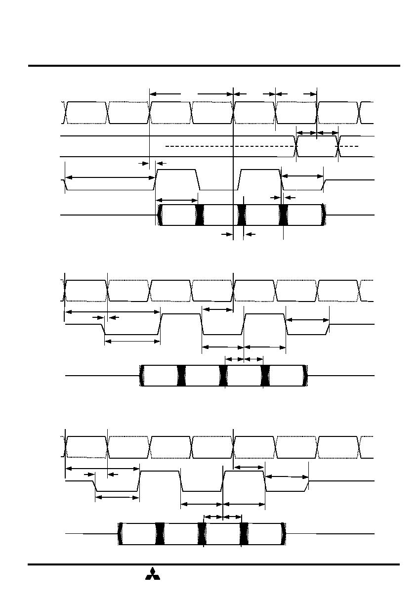
/CLK
DQS
tIS
tIH
VREF
CLK
Valid Data
Read Operation
tAC
tDQSCK
tCL
tCH
tCK
tDQSQ
tQH
tRPRE
tRPST
DQS
/CLK
CLK
tDQSS
tDS
tDH
tDQSL
tDQSH
tWPRE
Write Operation / tDQSS=max.
tDSS
tWPRES
tWPST
DQS
/CLK
CLK
tDQSS
tDS
tDH
tDQSL
tDQSH
tWPRE
Write Operation / tDQSS=min.
tDSH
tWPRES
tWPST
DQ
DQ
DQ
Cmd &
Add.

25
MITSUBISHI ELECTRIC
Mar. '02
MITSUBISHI LSIs
DDR SDRAM
(Rev.1.44)
M2S56D20/ 30/ 40ATP -75AL, -75A, -75L, -75, -10L, -10
256M Double Data Rate Synchronous DRAM
M2S56D20/ 30/ 40AKT -75AL, -75A, -75L, -75, -10L, -10
The DDR SDRAM has four independent banks. Each bank is activated by the ACT command with the bank
addresses (BA0,1). A row is indicated by the row address A12-0. The minimum activation interval between
banks is tRRD.
BANK ACTIVATE (ACT)
OPERATIONAL DESCRIPTION
The PRE command deactivates the bank indicated by BA0,1. When multiple banks are active, the precharge
all command (PREA,PRE+A10=H) is available to deactivate all banks at the same time. After tRP from the
precharge, an ACT command to the same bank can be issued.
PRECHARGE (PRE)
Bank Activation and Precharge All (BL=8, CL=2)
A precharge command can be issued after BL/2 time from a read command.
Precharge all
Command
A0-9,11
A10
BA0,1
DQ
ACT
Xa
Xa
00
READ
Y
0
00
ACT
Xb
Xb
01
PRE
tRRD
tRCD
1
ACT
Xb
Xb
01
tRAS
tRP
tRCmin
2 ACT command / tRCmin
DQS
Qa0
BL/2
Qa1 Qa2 Qa3 Qa4 Qa5 Qa6 Qa7
/CLK
CLK
26
MITSUBISHI ELECTRIC
Mar. '02
MITSUBISHI LSIs
DDR SDRAM
(Rev.1.44)
M2S56D20/ 30/ 40ATP -75AL, -75A, -75L, -75, -10L, -10
256M Double Data Rate Synchronous DRAM
M2S56D20/ 30/ 40AKT -75AL, -75A, -75L, -75, -10L, -10
After tRCD from the bank activation, a READ command can be issued. 1st Output data is available after the
/CAS Latency from the READ, followed by (BL-1) consecutive data. (BL : Burst Length) The start address is
specified by A11,A9-A0(x4)/A9-A0(x8)/A8-A0(x16), and the address sequence of burst data is defined by the
Burst Type. A READ command may be issued to any active bank, so the row precharge time (tRP) can be
hidden during the continuous burst data by interleaving the multiple banks. When A10 is high in READ
command, the auto-precharge (READA) is performed. Any command (READ,WRITE,PRE,ACT) asserted to
the same bank is inhibited till the internal precharge is completed. The internal precharge operation starts at
BL/2 time after READA command. The next ACT command can be issued after (BL/2+tRP) time from the
previous READA.
READ
Multi Bank Interleaving READ (BL=8, CL=2)
/CLK
Command
A0-9,11
A10
BA0,1
DQ
ACT
Xa
Xa
00
READ
Y
0
00
READ
Y
0
10
ACT
Xb
Xb
10
PRE
0
00
tRCD
/CAS latency
Burst Length
DQS
Qa0
CLK
Qa1 Qa2 Qa3 Qa4 Qa5 Qa6 Qa7 Qb0 Qb1 Qb2 Qb3 Qb4 Qb5 Qb7 Qb8
27
MITSUBISHI ELECTRIC
Mar. '02
MITSUBISHI LSIs
DDR SDRAM
(Rev.1.44)
M2S56D20/ 30/ 40ATP -75AL, -75A, -75L, -75, -10L, -10
256M Double Data Rate Synchronous DRAM
M2S56D20/ 30/ 40AKT -75AL, -75A, -75L, -75, -10L, -10
READ with Auto-Precharge (BL=8, CL=2,2.5)
A0-9,11
A10
BA0,1
DQ
Xa
Xa
00
Y
1
00
DQS
Internal Precharge starting Timing
Qa0 Qa1 Qa2 Qa3
Qa4 Qa5 Qa6 Qa7
DQ
DQS
Qa0 Qa1 Qa2 Qa3 Qa4 Qa5 Qa6 Qa7
CL=2
CL=2.5
tRCD
tRP
BL/2
BL/2 + tRP
Command
ACT
READA
/CLK
CLK
0
1
2
3
4
5
6
7
8
9
10
11
12
Operating description when new command is asserted.
Legal
Legal
Illegal
Illegal
Illegal
Illegal
Illegal
Illegal
WRITEA(CL=2.5)
Legal
Legal
Legal
Illegal
Illegal
Illegal
Illegal
Illegal
WRITE(CL=2)
Legal
Legal
Legal
Legal
Legal
Legal
Legal
Legal
PCG
Legal
Legal
Legal
Legal
Legal
Legal
Legal
Legal
ACT
Legal
Legal
Legal
Illegal
Illegal
Illegal
Illegal
Illegal
WRITEA(CL=2)
Legal
Legal
Illegal
Illegal
Illegal
Illegal
Illegal
Illegal
WRITE(CL=2.5)
Legal
Legal
Legal
Legal
Legal
Legal
Legal
Legal
READA
Legal
10
Legal
9
Legal
8
Legal
7
Legal
6
Legal
5
Legal
4
3
Legal
READ
For Different Bank
Asserted
Command
28
MITSUBISHI ELECTRIC
Mar. '02
MITSUBISHI LSIs
DDR SDRAM
(Rev.1.44)
M2S56D20/ 30/ 40ATP -75AL, -75A, -75L, -75, -10L, -10
256M Double Data Rate Synchronous DRAM
M2S56D20/ 30/ 40AKT -75AL, -75A, -75L, -75, -10L, -10
After tRCD time from the bank activation, a WRITE command can be issued. 1st input data is sampled at the
WRITE command with data strobe input, followed by (BL-1) data being written into RAM.The Burst Length is BL.
The start address is specified by A11,A9-A0(x4)/A9-A0(x8)/A8-A0(x16), and the address sequence of burst data
is defined by the Burst Type. A WRITE command may be applied to any active bank, so the row precharge time
(tRP) can be hidden during the continuous input data by interleaving the multiple banks. The write recovery time
(tWR) is required from the last written data to the next PRE command. When A10 is high in a WRITE command,
the auto-precharge(WRITEA) is performed. Any command (READ,WRITE,PRE,ACT) asserted to the same
bank is inhibited till the internal precharge operation is completed. The next ACT command can be issued after
tDAL from the last input data cycle.
WRITE
Multi Bank Interleaving WRITE (BL=8)
Command
A0-9,11
A10
BA0,1
DQ
ACT
Xa
00
WRITE
00
WRITE
0
0
10
ACT
Xb
10
0
10
tRCD
D
tRCD
D
PRE
Xa
0
00
PRE
DQS
/CLK
CLK
Da0 Da1 Da2 Da3 Da4 Da5
Da6 Da7 Db0 Db1 Db2 Db3
Db4 Db5 Db6 Db7
Xa
Ya
Yb
Xb
29
MITSUBISHI ELECTRIC
Mar. '02
MITSUBISHI LSIs
DDR SDRAM
(Rev.1.44)
M2S56D20/ 30/ 40ATP -75AL, -75A, -75L, -75, -10L, -10
256M Double Data Rate Synchronous DRAM
M2S56D20/ 30/ 40AKT -75AL, -75A, -75L, -75, -10L, -10
WRITE with Auto-Precharge (BL=8)
Command
A0-9,11
A10
BA0,1
DQ
ACT
Xa
00
WRITEA
1
00
ACT
Xb
00
tRCD
D
Da0
DQS
/CLK
CLK
Da1
Da2 Da3
Da4 Da5
Da6 Da7
tDAL
Xa
Y
Xb
Legal
Legal
Legal
Legal
Legal
Legal
Legal
Legal
PCG
Legal
Legal
Legal
Legal
Legal
Legal
Legal
Legal
ACT
Legal
Legal
Legal
Legal
Legal
Legal
Legal
Legal
WRITEA
Legal
Legal
Legal
Legal
Legal
Legal
Legal
Legal
WRITE
Legal
Legal
Legal
Illegal
Illegal
Illegal
Illegal
Illegal
READA
Legal
10
Legal
9
Legal
8
Illegal
7
Illegal
6
Illegal
5
Illegal
4
3
Illegal
READ
For Different Bank
Asserted
Command
0
1
2
3
4
5
6
7
8
9
10
11
12
Operating description when new command is asserted.
BL/2

30
MITSUBISHI ELECTRIC
Mar. '02
MITSUBISHI LSIs
DDR SDRAM
(Rev.1.44)
M2S56D20/ 30/ 40ATP -75AL, -75A, -75L, -75, -10L, -10
256M Double Data Rate Synchronous DRAM
M2S56D20/ 30/ 40AKT -75AL, -75A, -75L, -75, -10L, -10
BURST INTERRUPTION
[Read Interrupted by Read]
Burst read operation can be interrupted by the new Read command issued to any other bank.
Random column access is allowed. READ to READ interval is 1CLK as the minimum.
Read Interrupted by Read (BL=8, CL=2)
Command
A0-9,11
A10
BA0,1
DQ
Yi
READ READ
READ
READ
Yj
Yk
Yl
0
0
0
0
00
10
00
01
DQS
Qai0 Qai1 Qaj0 Qaj1 Qaj2 Qaj3 Qak0 Qak1 Qak2 Qak3 Qak4 Qak5 Qal0 Qal1 Qal2 Qal3 Qal4 Qal5 Qal6 Qal7
/CLK
CLK
[Read Interrupted by precharge]
Burst read operation can be interrupted by precharge of the same bank. READ to PRE interval is 1 CLK
minimum. The time between PRE command to output disable is equal to the CAS Latency. As a result,
READ to PRE interval determines valid data length to be outputted. The figure below shows the examples of
BL=8.
Read Interrupted by Precharge (BL=8)
CL=2.5
Command
DQS
Command
DQ
Command
DQ
Q0 Q1 Q2 Q3
Q0 Q1
/CLK
CLK
DQ
Q0 Q1 Q2 Q3 Q4 Q5
PRE
READ
READ
PRE
READ PRE
DQS
DQS

31
MITSUBISHI ELECTRIC
Mar. '02
MITSUBISHI LSIs
DDR SDRAM
(Rev.1.44)
M2S56D20/ 30/ 40ATP -75AL, -75A, -75L, -75, -10L, -10
256M Double Data Rate Synchronous DRAM
M2S56D20/ 30/ 40AKT -75AL, -75A, -75L, -75, -10L, -10
Read Interrupted by Precharge (BL=8)
CL=2.0
/CLK
CLK
Command
DQS
Command
DQ
Command
DQ
Q0 Q1 Q2 Q3
Q0 Q1
DQ
Q0 Q1 Q2 Q3 Q4 Q5
PRE
READ
READ
PRE
READ PRE
DQS
DQS
32
MITSUBISHI ELECTRIC
Mar. '02
MITSUBISHI LSIs
DDR SDRAM
(Rev.1.44)
M2S56D20/ 30/ 40ATP -75AL, -75A, -75L, -75, -10L, -10
256M Double Data Rate Synchronous DRAM
M2S56D20/ 30/ 40AKT -75AL, -75A, -75L, -75, -10L, -10
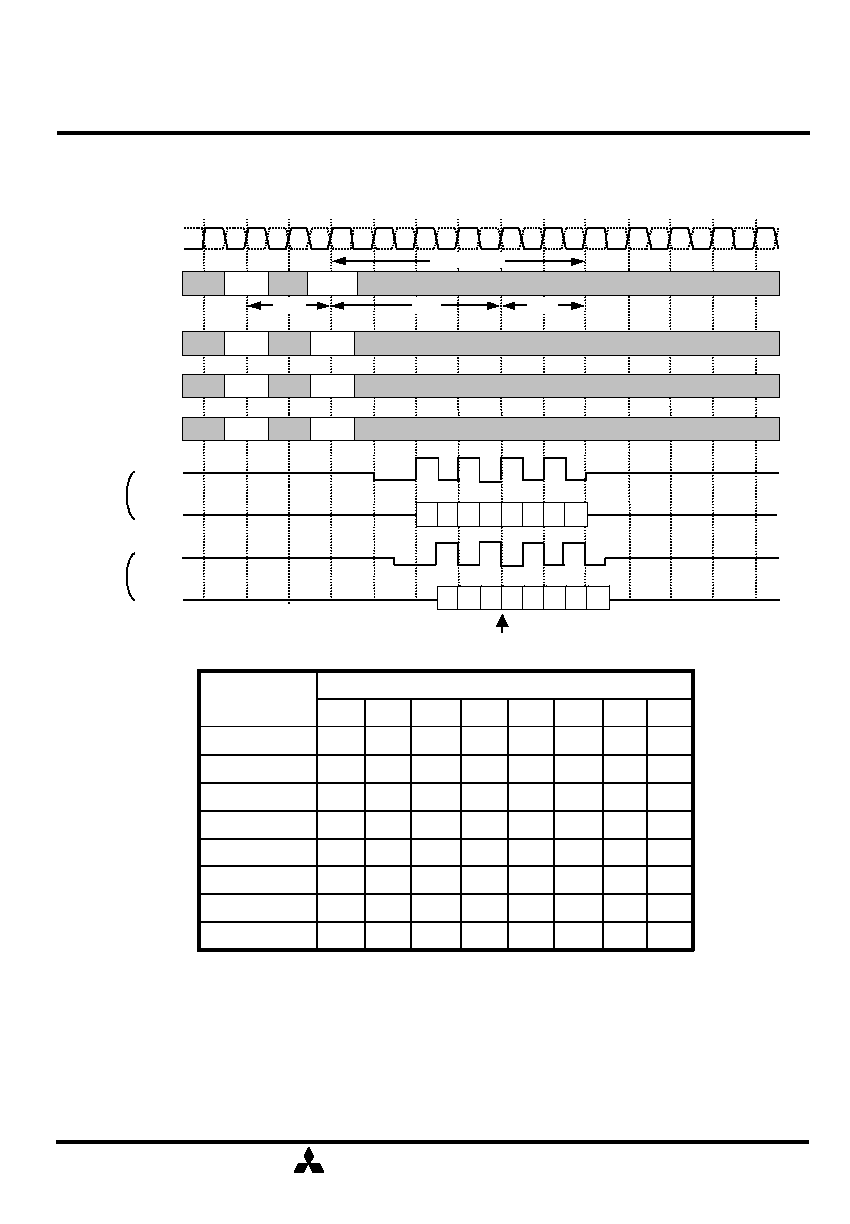
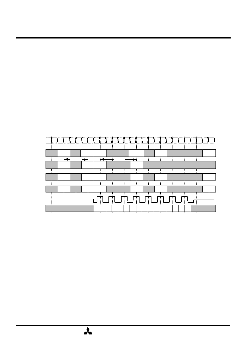
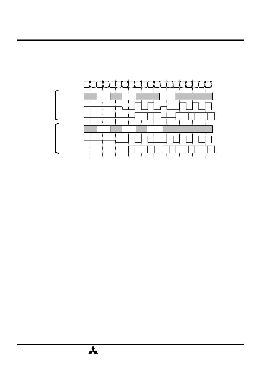
Burst read operation can be interrupted by a burst stop command(TERM). READ to TERM interval is 1 CLK
minimum. The time between TERM command to output disable is equal to the CAS Latency. As a result, READ
to TERM interval determines valid data length to be outputted. The figure below shows example of BL=8.
[Read Interrupted by Burst Stop]
Read Interrupted by TERM (BL=8)
CL=2.5
Command
DQS
Command
DQ
Command
DQ
Q0 Q1 Q2 Q3
Q0 Q1
/CLK
CLK
DQ
Q0 Q1 Q2 Q3 Q4 Q5
TERM
READ
READ
TERM
READ
TERM
DQS
DQS
CL=2.0
Command
DQS
Command
DQ
Command
DQ
Q0 Q1 Q2 Q3
Q0 Q1
DQ
Q0 Q1 Q2 Q3 Q4 Q5
TERM
READ
READ
TERM
READ
TERM
DQS
DQS
33
MITSUBISHI ELECTRIC
Mar. '02
MITSUBISHI LSIs
DDR SDRAM
(Rev.1.44)
M2S56D20/ 30/ 40ATP -75AL, -75A, -75L, -75, -10L, -10
256M Double Data Rate Synchronous DRAM
M2S56D20/ 30/ 40AKT -75AL, -75A, -75L, -75, -10L, -10
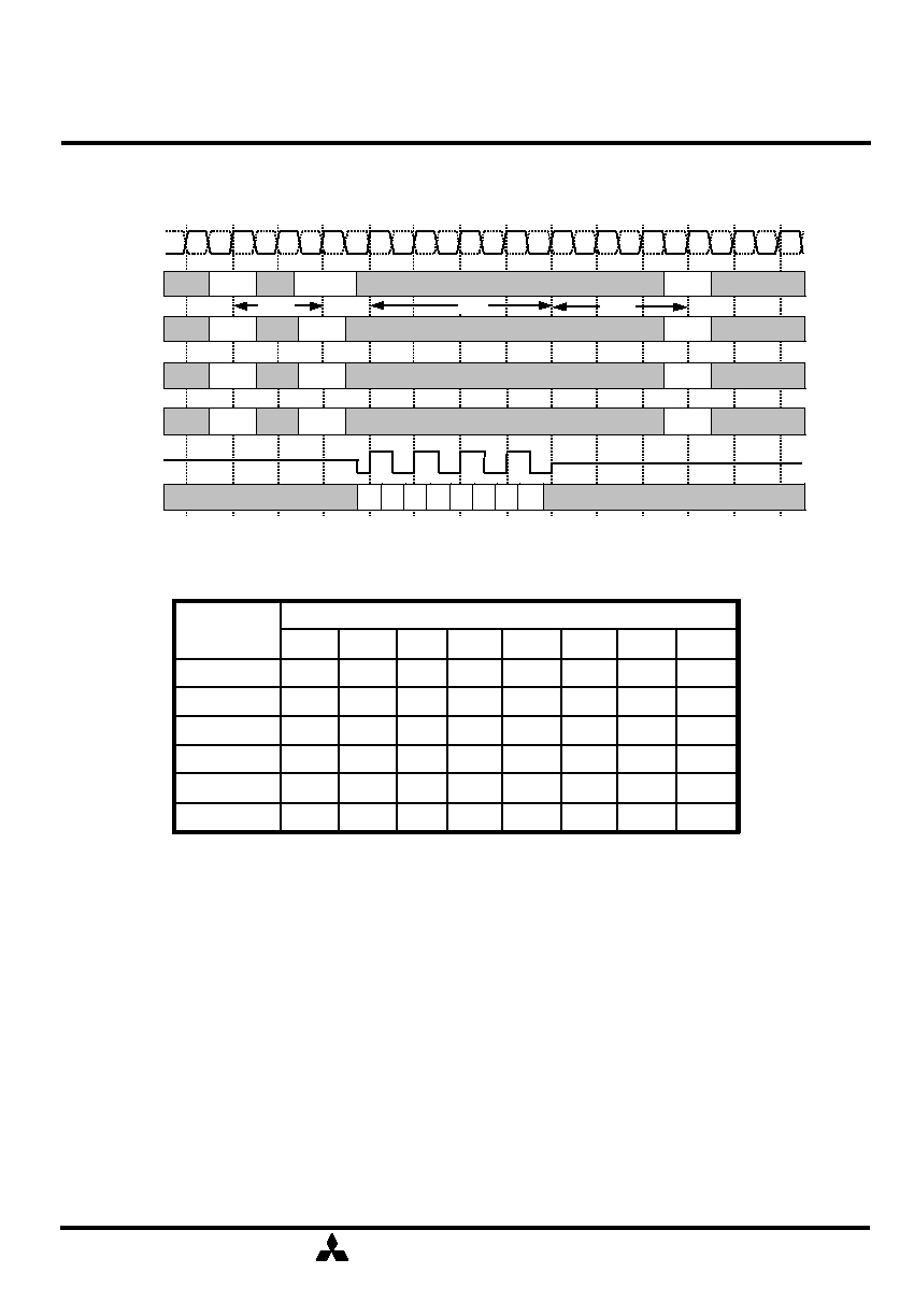
[Read Interrupted by Write with TERM]
Read Interrupted by TERM (BL=8)
CL=2.5
Command
DQ
Q0 Q1 Q2 Q3
/CLK
CLK
READ
TERM
DQS
WRITE
D0 D1 D2 D3 D4 D5
CL=2.0
Command
DQ
Q0 Q1 Q2 Q3
READ
TERM
DQS
WRITE
D0 D1 D2 D3 D4 D5 D6 D7

34
MITSUBISHI ELECTRIC
Mar. '02
MITSUBISHI LSIs
DDR SDRAM
(Rev.1.44)
M2S56D20/ 30/ 40ATP -75AL, -75A, -75L, -75, -10L, -10
256M Double Data Rate Synchronous DRAM
M2S56D20/ 30/ 40AKT -75AL, -75A, -75L, -75, -10L, -10
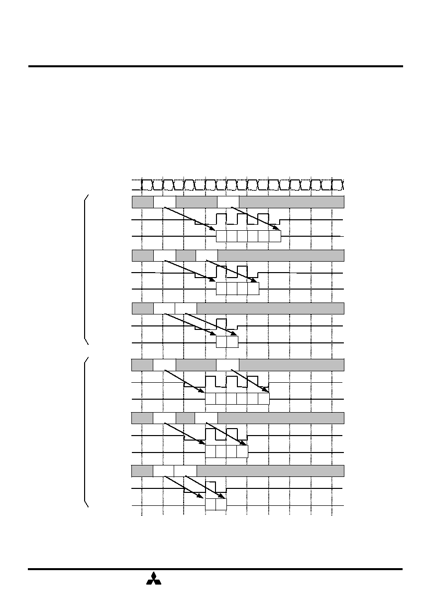
Burst write operation can be interrupted by Write to any bank. Random column access is allowed. WRITE
to WRITE interval is 1 CLK minimum.
[Write interrupted by Write]
[Write interrupted by Read]
Burst write operation can be interrupted by read of the same or the other bank. Random column access is
allowed. Internal WRITE to READ command interval(tWTR) is 1 CLK minimum. The input data masked by
DM in the interrupted READ cycle is "don't care". tWTR is referenced from the first positive edge after the last
data input.
Write Interrupted by Read (BL=8, CL=2.5)
Command
A0-9,11
A10
BA0,1
DQ
WRITE
Yi
0
00
READ
Yj
0
00
Dai0 Dai1
Qaj0 Qaj1 Qaj2 Qaj3
QS
Qaj4 Qaj5 Qaj6
Qaj7
DM
tWTR
/CLK
CLK
Write Interrupted by Write (BL=8)
Command
A0-9,11
A10
BA0,1
WRITE
Yi
0
00
WRITE
Yk
0
10
WRITE
Yj
0
00
WRITE
Yl
0
00
DQ
Dai1
Daj1
Daj3
Dak1
Dak3
Dak5
Dal1
DQS
Dal2 Dal3
Dal5 Dal6
Dal7
Dal4
Dal0
Dak4
Dak2
Dak0
Dai0
Daj0
Daj2
/CLK
CLK
35
MITSUBISHI ELECTRIC
Mar. '02
MITSUBISHI LSIs
DDR SDRAM
(Rev.1.44)
M2S56D20/ 30/ 40ATP -75AL, -75A, -75L, -75, -10L, -10
256M Double Data Rate Synchronous DRAM
M2S56D20/ 30/ 40AKT -75AL, -75A, -75L, -75, -10L, -10
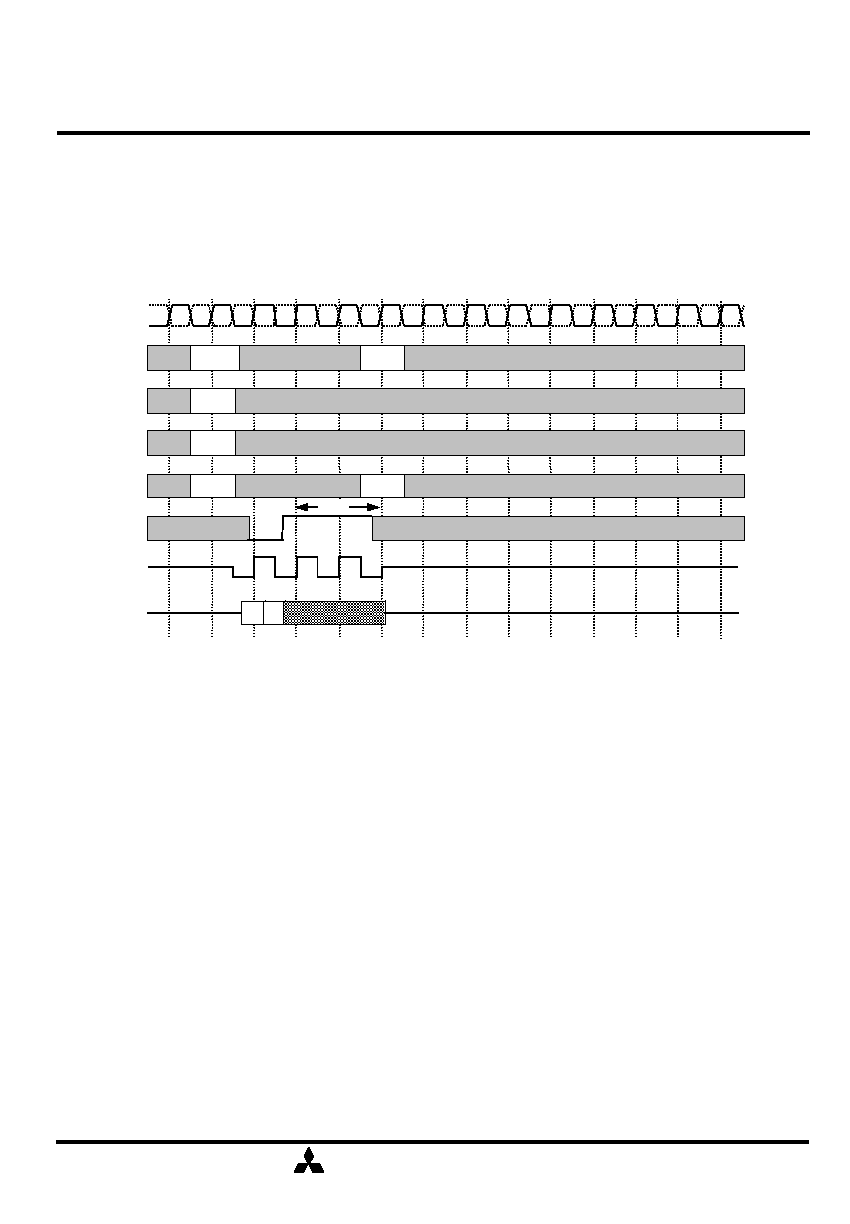
Burst write operation can be interrupted by precharge of the same or all bank. Random column access is
allowed. tWR is referenced from the first positive CLK edge after the last data input.
[Write interrupted by Precharge]
Write Interrupted by Precharge (BL=8, CL=2.5)
Command
A0-9,11
A10
BA0,1
DQ
WRITE
Yi
0
00
PRE
00
Dai0 Dai1
QS
DM
tWR
/CLK
CLK
36
MITSUBISHI ELECTRIC
Mar. '02
MITSUBISHI LSIs
DDR SDRAM
(Rev.1.44)
M2S56D20/ 30/ 40ATP -75AL, -75A, -75L, -75, -10L, -10
256M Double Data Rate Synchronous DRAM
M2S56D20/ 30/ 40AKT -75AL, -75A, -75L, -75, -10L, -10
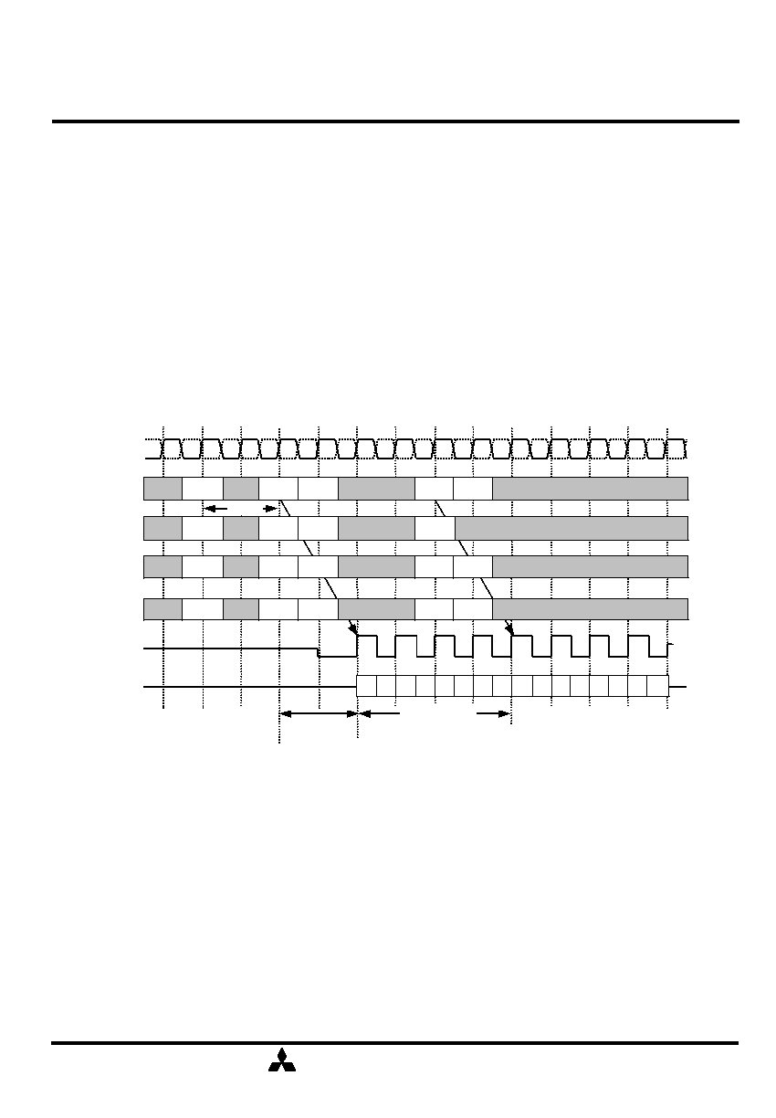
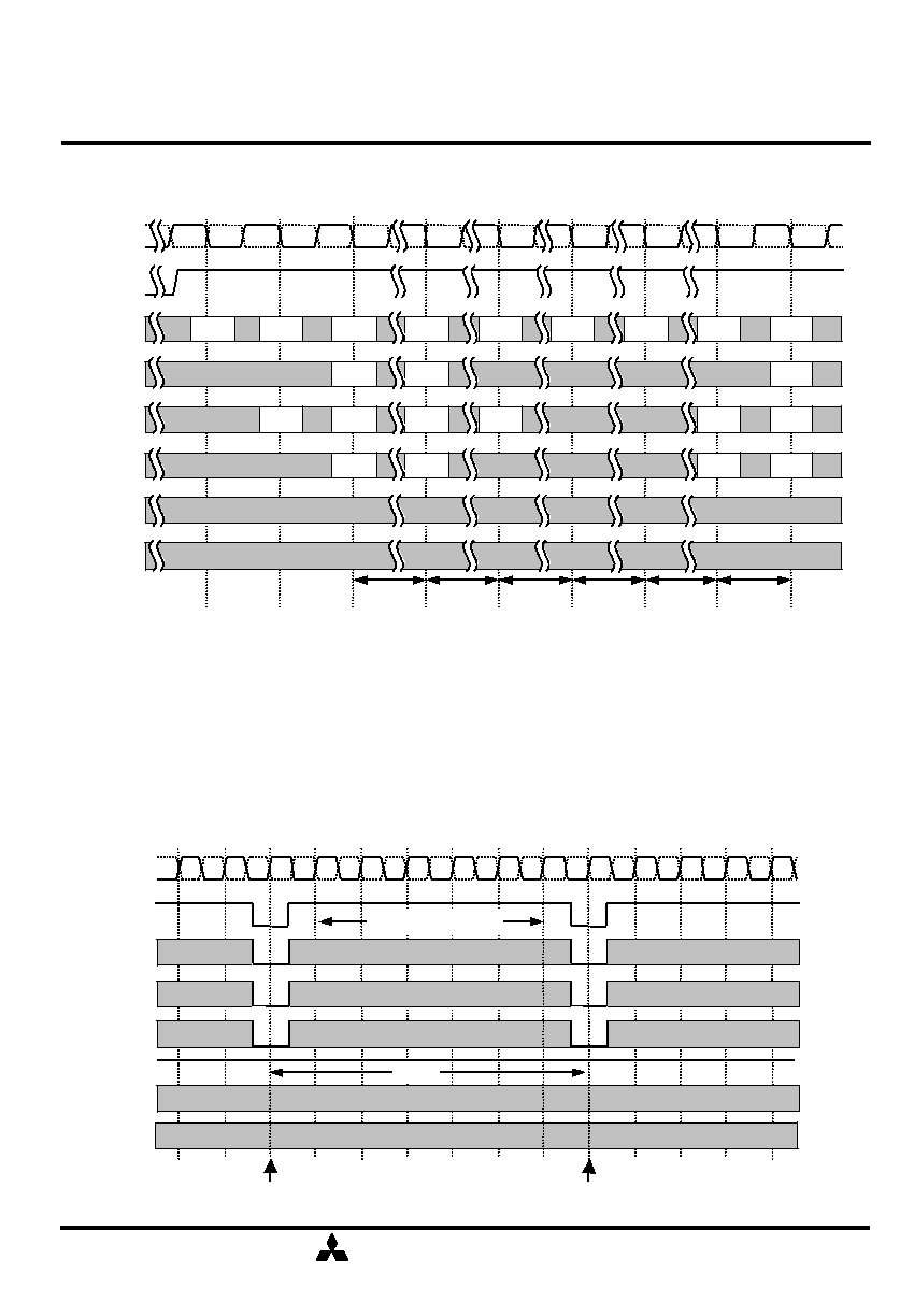
[Initialize and Mode Register sets]
Command
/CLK
CLK
EMRS
PRE
NOP
MRS
PRE
AR
AR
MRS
ACT
Code
Code
Xa
Code
Xa
1 0
Xa
A0-9,11
A10
Code
1
BA0,1
DQS
DQ
1
0 0
0 0
Code
tMRD
tMRD
tRP
tRFC
tRFC
tMRD
Mode Register Set,
Reset DLL
Extended Mode
Register Set
[AUTO REFRESH]
Auto-refresh cycle is initiated with a REFA(/CS=/RAS=/CAS=L,/WE=CKE=H) command.
The refresh address is generated internally. 8192 REFA cycles within 64ms refresh
256 Mbits memory cells. The auto-refresh is performed on 4 banks concurrently. Before performing an auto
refresh, all banks must be in the idle state. The minimum internal between auto-refresh is tRFC . No
command is allowed within tRFC time after the REFA command.
Auto-Refresh
/RAS
CKE
/CS
/CAS
/WE
A0-11
BA0,1
NOP or DESELECT
tRFC
Auto Refresh on All Banks
Auto Refresh on All Banks
/CLK
CLK
CKE
Initialize and MRS
37
MITSUBISHI ELECTRIC
Mar. '02
MITSUBISHI LSIs
DDR SDRAM
(Rev.1.44)
M2S56D20/ 30/ 40ATP -75AL, -75A, -75L, -75, -10L, -10
256M Double Data Rate Synchronous DRAM
M2S56D20/ 30/ 40AKT -75AL, -75A, -75L, -75, -10L, -10
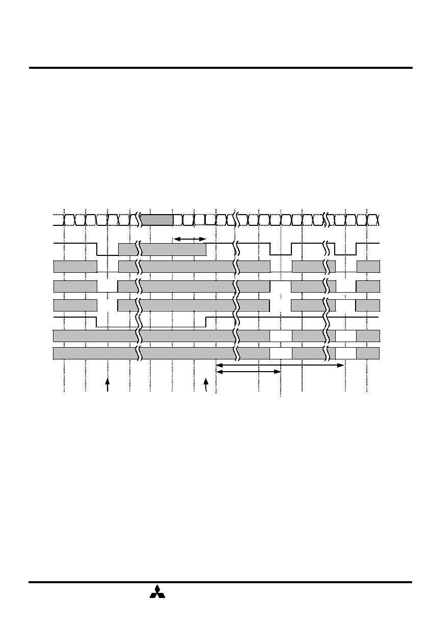
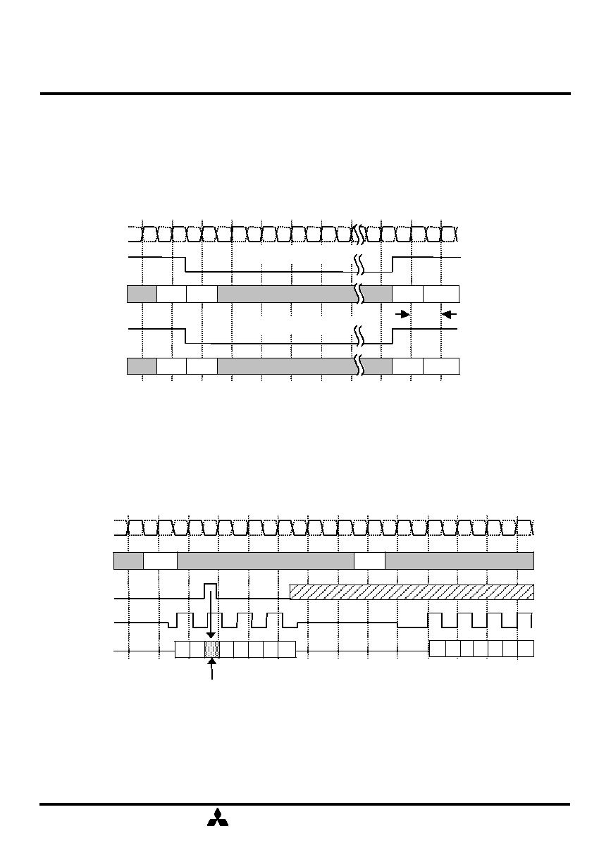
[SELF REFRESH]
Self -refresh mode is entered by asserting a REFS command (/CS=/RAS=/CAS=L,/WE=H,CKE=L). The self-
refresh mode is maintained as long as CKE is kept low. During the self-refresh mode, CKE becomes
asynchronous and the only enable input. All other inputs including CLK are disabled and ignored to save the
power
consumption. In order to exit the self-refresh mode, the device shall be supplied the stable CLK inputs,
followed by DESEL or NOP command, then asserting CKE for the period longer than tXSNR/tXSRD.
Self-Refresh
/RAS
CKE
/CS
/CAS
/WE
A0-11
BA0,1
tXSNR
Self Refresh Exit
/CLK
CLK
X
Y
X
Y
tXSRD
Stable CLK
Self Refresh Entry
38
MITSUBISHI ELECTRIC
Mar. '02
MITSUBISHI LSIs
DDR SDRAM
(Rev.1.44)
M2S56D20/ 30/ 40ATP -75AL, -75A, -75L, -75, -10L, -10
256M Double Data Rate Synchronous DRAM
M2S56D20/ 30/ 40AKT -75AL, -75A, -75L, -75, -10L, -10
The purpose of CLK suspend is power down. CKE is synchronous input except during the self-refresh mode. A
commands are ignored. From CKE=H to normal function, DLL recovery time is NOT required when the stable
CLK is supplied during the power down mode.
[Power DOWN]
/CLK
CLK
Power Down by CKE
Command
PRE
CKE
Command
ACT
CKE
Standby Power Down
NOP
NOP
Valid
NOP
NOP
Valid
Active Power Down
DM is defined as the data mask for write data. During writes, DM masks the input data cycle by cycle. Latency
of DM to write mask is 0.
[DM CONTROL]
DM Function(BL=8,CL=2)
Command
DQS
DQ
DM
WRITE
READ
D0 D1
D3 D4 D5 D6
D7
masked by DM=H
Don't Care
Q2 Q3 Q4 Q5
/CLK
CLK
Q0 Q1
Q6
tXPNR/tXPRD

39
MITSUBISHI ELECTRIC
Mar. '02
MITSUBISHI LSIs
DDR SDRAM
(Rev.1.44)
M2S56D20/ 30/ 40ATP -75AL, -75A, -75L, -75, -10L, -10
256M Double Data Rate Synchronous DRAM
M2S56D20/ 30/ 40AKT -75AL, -75A, -75L, -75, -10L, -10
Keep safety first in your circuit designs!
Mitsubishi Electric Corporation puts the maximum effort into making semiconductor products better and more
reliable, but there is always the possibility that trouble may occur with them. Trouble with semiconductors may
lead to personal injury, fire or property damage. Remember to give due consideration to safety when making
your circuit designs, with appropriate measures such as (i) placement of substitutive, auxiliary circuits, (ii) use of
non-flammable material or (iii) prevention against any malfunction or mishap.
Notes regarding these materials
These materials are intended as a reference to assist our customers in the selection of the Mitsubishi
semiconductor product best suited to the customer's application; they do not convey any license under any
intellectual property rights, or any other rights, belonging to Mitsubishi Electric Corporation or a third party.
Mitsubishi Electric Corporation assumes no responsibility for any damage, or infringement of any third-party's
rights, originating in the use of any product data, diagrams, charts, programs, algorithms, or circuit application
examples contained in these materials.
All information contained in these materials, including product data, diagrams, charts, programs and algorithms
represents information on products at the time of publication of these materials, and are subject to change by
Mitsubishi Electric Corporation without notice due to product improvements or other reasons. It is therefore
recommended that customers contact Mitsubishi Electric Corporation or an authorized Mitsubishi
Semiconductor product distributor for the latest product information before purchasing a product listed herein.
The information described here may contain technical inaccuracies or typographical errors. Mitsubishi Electric
Corporation assumes no responsibility for any damage, liability, or other loss rising from these inaccuracies or
errors.
Please also pay attention to information published by Mitsubishi Electric Corporation by various means,
including the Mitsubishi Semiconductor home page (
http://www.mitsubishichips.com)
.
When using any or all of the information contained in these materials, including product data, diagrams, charts,
programs, and algorithms, please be sure to evaluate all information as a total system before making a final
decision on the applicability of the information and products. Mitsubishi Electric Corporation assumes no
responsibility for any damage, liability or other loss resulting from the information contained herein.
Mitsubishi Electric Corporation semiconductors are not designed or manufactured for use in a device or system
that is used under circumstances in which human life is potentially at stake. Please contact Mitsubishi Electric
Corporation or an authorized Mitsubishi Semiconductor product distributor when considering the use of a
product contained herein for any specific purposes, such as apparatus or systems for transportation, vehicular,
medical, aerospace, nuclear, or undersea repeater use.
The prior written approval of Mitsubishi Electric Corporation is necessary to reprint or reproduce in whole or in
part these materials.
If these products or technologies are subject to the Japanese export control restrictions, they must be exported
under a license from the Japanese government and cannot be imported into a country other than the approved
destination.
Any diversion or reexport contrary to the export control laws and regulations of Japan and/or the country of
destination is prohibited.
Please contact Mitsubishi Electric Corporation or an authorized Mitsubishi Semiconductor product distributor for
further details on these materials or the products contained therein.

40
MITSUBISHI ELECTRIC
Mar. '02
MITSUBISHI LSIs
DDR SDRAM
(Rev.1.44)
M2S56D20/ 30/ 40ATP -75AL, -75A, -75L, -75, -10L, -10
256M Double Data Rate Synchronous DRAM
M2S56D20/ 30/ 40AKT -75AL, -75A, -75L, -75, -10L, -10
Revision History
- Add Low power version Spec.
- Overshoot / Undershoot Spec Add
Mar.'02
1.44
-Unify *ATP's spec. with *AKT's spec. (Add *AKT spec to *ATP spec.)
-Change page 37 (Fig. : Self Refresh)
-Change IDD7 measurement timing (page 23:Note 20)
-Modify Average Supply Current from VDD
-75A / -75 /-10 -75A & -75 / -10
IDD0 X4 Limits (from 105 / 105 / 120mA to 85 / 75mA)
IDD0 X8 Limits (from 110 / 110 / 120mA to 85 / 75mA)
IDD0 X16 Limits (from 120 / 120 / 115mA to 85 / 75mA)
IDD1 X4 Limits (from 110 / 110 / 105mA to 95 / 85mA)
IDD1 X8 Limits (from 115 / 115 / 110mA to 100 / 90mA)
IDD1 X16 Limits (from 135 / 135 / 130mA to 115 / 105mA)
IDD2P Limits (from 20 / 20 / 20mA to 6 / 6mA)
IDD2F Limits (from 40 / 40 / 40mA to 30 / 25mA)
IDD3P Limits (from 30 / 30 / 30mA to 15 / 12mA)
IDD3N X4 Limits (from 60 / 60 / 55mA to 45 / 35mA)
IDD3N X8 Limits (from 65 / 65 / 60mA to 45 / 35mA)
IDD3N X16 Limits (from 75 / 75 / 70mA to 45 / 35mA)
IDD4R X4 Limits (from 150 / 150 / 140mA to 140 / 100mA)
IDD4R X8 Limits (from 170 / 170 / 160mA to 150 / 115mA)
IDD4R X16 Limits (from 210 / 210 / 200mA to 180 / 145mA)
IDD4W X4 Limits (from 145 / 145 / 135mA to 130 / 95mA)
IDD4W X8 Limits (from 165 / 165 / 155mA to 140 / 105mA)
IDD4W X16 Limits (from 200 / 200 / 180mA to 160 / 120mA)
IDD5 Limits (from 185 / 185 / 175mA to 140 / 130mA)
IDD7 X4 Limits (from 250 / 250 / 230mA to 215 / 170mA)
IDD7 X8 Limits (from 260 / 260 / 240mA to 235 / 185mA)
IDD7 X16 Limits (from 290 / 290 / 280mA to 270 / 210mA)
Jan.`02
1.33
-Added Operating description Table when new command asserted while write &
read with auto precharge is issued.
Jun.'01
1.2
Jun.'01
May '01
Date
-Added -75A Spec.
-Added IDD7 Spec.
-Changed VIH(DC)min Spec. from VREF+0.18V to VREF+0.15V
-Changed VIL(DC)min Spec. from VREF-0.18V to VREF-0.15V
-Changed VIH(AC)min Spec. from VREF+0.35V to VREF+0.31V
-Changed VIL(AC)max Spec. from VREF-0.35V to VREF-0.31V
-Changed IOH Spec. from -15.2mA to -16.8mA
-Changed IOL Spec. from +15.2mA to +16.8mA
1.1
-New registration (May. `01)
1.02
Description
Rev.