M2V28S20TP-6,-7,-8
M2V28S30TP-6,-7,-7L,-8,-8L
M2V28S40TP-7,-7L,-8,-8L
Jun. '99
MITSUBISHI LSIs
SDRAM (Rev. 1.0E)
128M Synchronous DRAM
(4-BANK x 8,388,608-WORD x 4-BIT)
(4-BANK x 4,194,304-WORD x 8-BIT)
(4-BANK x 2,097,152-WORD x 16-BIT)
MITSUBISHI ELECTRIC
1
DESCRIPTION
M2V28S20TP is organized as 4-bank x 8,388,608-word x 4-bit Synchronous DRAM with LVTTL
interface and M2V28S30TP is organized as 4-bank x 4,194,304-word x 8-bit and M2V28S40TP is organized as
4-bank x 2,097,152-word x 16-bit. All inputs and outputs are referenced to the rising edge of CLK.
M2V28S20TP,M2V28S30TP,M2V28S40TP achieves very high speed data rates up to 133MHz, and is
suitable for main memory or graphic memory in computer systems.
FEATURES
- Single 3.3V ±0.3V power supply
- Max. Clock frequency
-6:PC133<3-3-3> / -7:PC100<2-2-2> / -8:PC100<3-2-2>
- PC133(-6) supports x4/x8 only. And does not support Low-Power (L) version.
- Fully synchronous operation referenced to clock rising edge
- 4-bank operation controlled by BA0,BA1(Bank Address)
- /CAS latency- 2/3 (programmable)
- Burst length- 1/2/4/8/FP (programmable)
- Burst type- Sequential and interleave burst (programmable)
- Byte Control- DQML and DQMU (M2V28S40TP)
- Random column access
- Auto precharge / All bank precharge controlled by A10
- Auto and self refresh
- 4096 refresh cycles /64ms
- LVTTL Interface
- Package
M2V28S20TP/30TP/40TP
400-mil, 54-pin Thin Small Outline (TSOP II) with 0.8mm lead pitch
PRELIMINARY
Some of contents are described for general products and are
subject to change without notice.
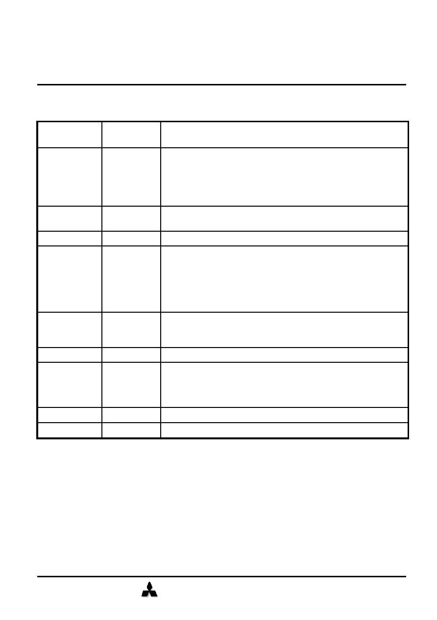
ITEM
tCLK
M2V28S20/30/40TP
-7
-8
tRAS
tRCD
tAC
tRC
Icc1
Icc6
Clock Cycle Time
(Min.)
Active to Precharge Command Period
(Min.)
Row to Column Delay
(Min.)
Access Time from CLK
(Max.) (CL=3)
Ref/Active Command Period
(Min.)
Operation Current
(Max.)
(Single Bank)
Self Refresh Current
(Max.)
10ns
50ns
20ns
6ns
70ns
2mA
10ns
50ns
20ns
6ns
70ns
2mA
V28S20
V28S30
V28S40
-6
7.5ns
45ns
20ns
5.4ns
67.5ns
2mA
130mA
-
120mA
135mA
120mA
135mA
120mA
115mA
115mA
M2V28S20TP-6,-7,-8
M2V28S30TP-6,-7,-7L,-8,-8L
M2V28S40TP-7,-7L,-8,-8L
Jun. '99
MITSUBISHI LSIs
SDRAM (Rev. 1.0E)
128M Synchronous DRAM
(4-BANK x 8,388,608-WORD x 4-BIT)
(4-BANK x 4,194,304-WORD x 8-BIT)
(4-BANK x 2,097,152-WORD x 16-BIT)
MITSUBISHI ELECTRIC
2
Rev.
Revision History
Description
1.0
- Add PC133 Specification.
M2V28S20TP-6,-7,-8
M2V28S30TP-6,-7,-7L,-8,-8L
M2V28S40TP-7,-7L,-8,-8L
Jun. '99
MITSUBISHI LSIs
SDRAM (Rev. 1.0E)
128M Synchronous DRAM
(4-BANK x 8,388,608-WORD x 4-BIT)
(4-BANK x 4,194,304-WORD x 8-BIT)
(4-BANK x 2,097,152-WORD x 16-BIT)
MITSUBISHI ELECTRIC
3
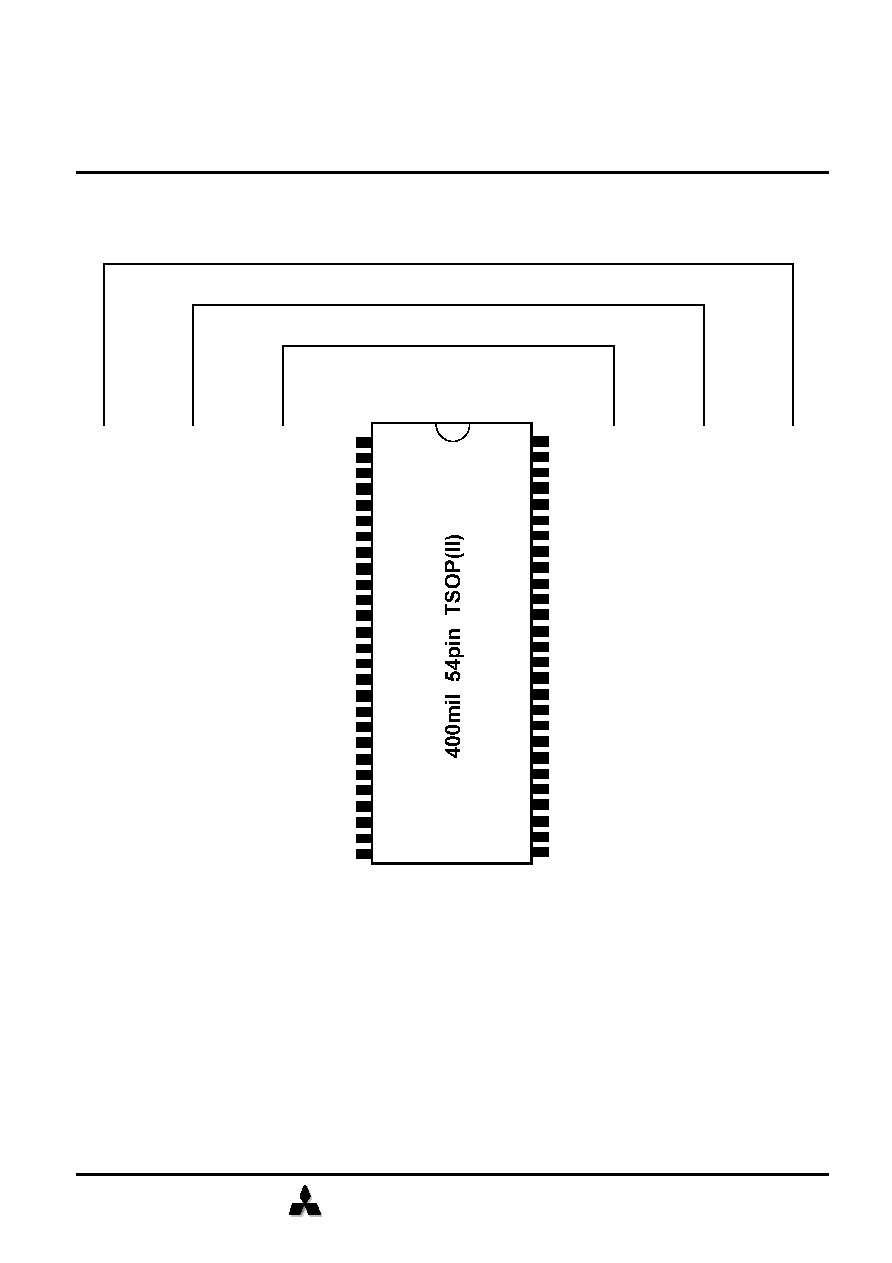
PIN CONFIGURATION (TOP VIEW)
M2V28S30TP
M2V28S40TP
PIN CONFIGURATION
(TOP VIEW)
1
2
3
4
5
6
7
8
9
10
11
12
13
14
15
16
17
18
19
20
21
22
54
53
52
51
50
49
48
47
46
45
44
43
42
41
40
39
38
37
36
35
34
33
23
32
24
31
25
30
26
29
27
28
Vdd
DQ0
VddQ
DQ1
DQ2
VssQ
DQ3
DQ4
VddQ
DQ5
DQ6
VssQ
DQ7
Vdd
DQML
/WE
/CAS
/RAS
/CS
BA0(A13)
BA1(A12)
A10(AP)
A2
A3
Vdd
A0
A1
Vss
DQ15
VssQ
DQ14
DQ13
VddQ
DQ12
DQ11
VssQ
DQ10
DQ9
VddQ
DQ8
Vss
NC
DQMU
CLK
CKE
NC
A11
A8
A7
A6
A5
A4
Vss
A9
Vdd
DQ0
VddQ
NC
DQ1
VssQ
NC
DQ2
VddQ
NC
DQ3
VssQ
NC
Vdd
NC
/WE
/CAS
/RAS
/CS
BA0(A13)
BA1(A12)
A10(AP)
A2
A3
Vdd
A0
A1
Vdd
NC
VddQ
NC
DQ0
VssQ
NC
NC
VddQ
NC
DQ1
VssQ
NC
Vdd
NC
/WE
/CAS
/RAS
/CS
BA0(A13)
BA1(A12)
A10(AP)
A2
A3
Vdd
A0
A1
Vss
DQ7
VssQ
NC
DQ6
VddQ
NC
DQ5
VssQ
NC
DQ4
VddQ
NC
Vss
NC
DQM
CLK
CKE
NC
A11
A8
A7
A6
A5
A4
Vss
A9
Vss
NC
VssQ
NC
DQ3
VddQ
NC
NC
VssQ
NC
DQ2
VddQ
NC
Vss
NC
DQM
CLK
CKE
NC
A11
A8
A7
A6
A5
A4
Vss
A9
M2V28S20TP
CLK
: Master Clock
CKE
: Clock Enable
/CS
: Chip Select
/RAS
: Row Address Strobe
/CAS
: Column Address Strobe
/WE
: Write Enable
DQ0-15
: Data I/O
DQM
: Output Disable/ Write Mask
A0-11
: Address Input
BA0,1
: Bank Address
Vdd
: Power Supply
VddQ
: Power Supply for Output
Vss
: Ground
VssQ
: Ground for Output
M2V28S20TP-6,-7,-8
M2V28S30TP-6,-7,-7L,-8,-8L
M2V28S40TP-7,-7L,-8,-8L
Jun. '99
MITSUBISHI LSIs
SDRAM (Rev. 1.0E)
128M Synchronous DRAM
(4-BANK x 8,388,608-WORD x 4-BIT)
(4-BANK x 4,194,304-WORD x 8-BIT)
(4-BANK x 2,097,152-WORD x 16-BIT)
MITSUBISHI ELECTRIC
4
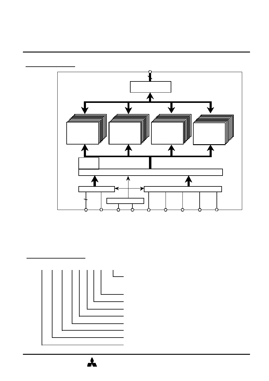
BLOCK DIAGRAM
Type Designation Code
M2 V 28 S 3 0
TP -8
Access Item
-6 : 7.5ns (PC133/3-3-3),
-7 : 10ns(PC100/2-2-2),
-8 : 10ns(PC100/3-2-2)
Package Type
TP : TSOP(II)
Process Generation Blank : 1st gen.
Interface
V : LVTTL
Organization
2: x4, 3: x8, 4: x16
Synchronous DRAM
Density
28 : 128Mbit
Function 0 : Random Column
Mitsubishi DRAM
These rules are only applied to the Synchronous DRAM family.
Note : This figure shows the M2V28S30TP.
The M2V28S20TP configration is 4096x2048x4 of cell array and DQ 0-3.
The M2V28S40TP configration is 4096x512x16 of cell array and DQ 0-15.
Address Buffer
A0-11
BA0,1
Control Signal Buffer
/CS
/RAS
/CAS
/WE
CLK
CKE
Clock Buffer
Control Circuitry
I/O Buffer
DQ0-7
Mode
Register
DQM
Memory Array
Bank #0
4096 x1024 x8
Cell Array
Memory Array
Bank #1
4096 x1024 x8
Cell Array
Memory Array
Bank #2
4096 x1024 x8
Cell Array
Memory Array
Bank #3
4096 x1024 x8
Cell Array
M2V28S20TP-6,-7,-8
M2V28S30TP-6,-7,-7L,-8,-8L
M2V28S40TP-7,-7L,-8,-8L
Jun. '99
MITSUBISHI LSIs
SDRAM (Rev. 1.0E)
128M Synchronous DRAM
(4-BANK x 8,388,608-WORD x 4-BIT)
(4-BANK x 4,194,304-WORD x 8-BIT)
(4-BANK x 2,097,152-WORD x 16-BIT)
MITSUBISHI ELECTRIC
5
PIN FUNCTION
CLK
Input
Master Clock:
All other inputs are referenced to the rising edge of CLK.
CKE
Input
Clock Enable:
CKE controls internal clock. When CKE is low, internal clock for the
following cycle is ceased. CKE is also used to select auto /
selfrefresh. After self refresh mode is started, CKE becomes
synchronous input. Self refresh is maintained as long as CKE is low.
/CS
Input
Chip Select:
When /CS is high, any command means No Operation.
/RAS, /CAS, /WE
Input
Combination of /RAS, /CAS, /WE defines basic commands.
A0-11
Input
A0-11 specify the Row / Column Address in conjunction with BA0,1.
The Row Address is specified by A0-11. The Column Address is
specified by A0-9,11 (x4) / A0-9 (x8) / A0-8 (x16).
A10 is also used to indicate precharge option. When A10 is high at a
read / write command, an auto precharge is performed. When A10 is
high at a precharge command, all banks are precharged.
BA0,1
Input
Bank Address:
BA0,1 specifies one of four banks to which a command is applied.
BA0,1 must be set with ACT, PRE, READ, WRITE commands.
DQ0-7
Input / Output
DQM
Input
Din Mask / Output Disable:
When DQM is high in burst write, Din for the current cycle is masked.
When DQM is high in burst read, Dout is disabled at the next but one
cycle.
Vdd, Vss
Power Supply
Power Supply for the memory array and peripheral circuitry.
VddQ, VssQ
Power Supply
VddQ and VssQ are supplied to the Output Buffers only.
Data In and Data out are referenced to the rising edge of CLK.