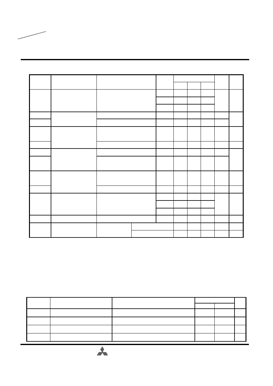
M2V56S20/ 30/ 40 TP ≠5,-5L, -6,-6L, -7,-7L
SDRAM (Rev.1.5E)
Single Data Rate
Oct.2001
256M Synchronous DRAM
MITSUBISHI LSIs
Preliminary
MITSUBISHI ELECTRIC
1
Some of contents are subject to change without notice.
DESCRIPTION
M2V56S20TP is a 4-bank x 16777216-word x 4-bit,
M2V56S30TP is a 4-bank x 8388608-word x 8-bit,
M2V56S40TP is a 4-bank x 4194304-word x 16-bit,
synchronous DRAM, with LVTTL interface.All inputs and outputs are referenced to the rising edge of
CLK.The M2V56S20/30/40TP achieve very high speed data rate up to 100MHz(-7) ,133MHz(-6) ,
166MHz(-5) and are suitable for main memory or graphic memory in computer systems.
FEATURES
-Single 3.3v±0.3V power supply
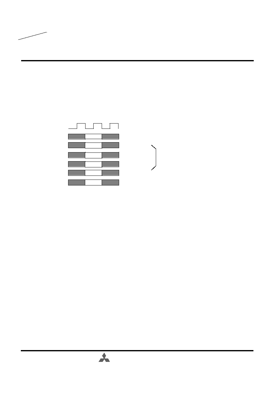
-Max. Clock frequency ≠5:PC166<3-3-3> / -6:PC133 <3-3-3> / -7:PC100 <2-2-2>
Synchronous operation referenced to clock -Fully rising edge
-Single Data Rate
-4 bank operation controlled by BA0, BA1 (Bank Address)
-/CAS latency- 2/3 (programmable)
-Burst length- 1/2/4/8/full page (programmable)
-Burst type- sequential / interleave (programmable)
-Random column access
-Auto precharge / All bank precharge controlled by A10
-8192 refresh cycles / 64ms (4 banks concurrent refresh)
-Auto refresh and Self refresh
-Row address A0-12 / Column address A0-9,11(x4)/ A0-9(x8)/ A0-8(x16)
-LVTTL Interface
-400-mil, 54-pin Thin Small Outline Package (TSOPII) with 0.8mm lead pitch
Max. Frequency
Max. Frequency
@CL2
@CL3
M2V56S20/30/40TP-5/-5L
133MHz
166MHz
PC133(CL2)
M2V56S20/30/40TP-6/-6L
100MHz
133MHz
PC133(CL3)
M2V56S20/30/40TP-7/-7L
100MHz
100MHz
PC100(CL2)
Standard
Note: The ≠5L/-6L/-7L is selfrefresh low power.
M2V56S20/ 30/ 40 TP ≠5,-5L, -6,-6L, -7,-7L
SDRAM (Rev.1.5E)
Single Data Rate
Oct.2001
256M Synchronous DRAM
MITSUBISHI LSIs
Preliminary
MITSUBISHI ELECTRIC
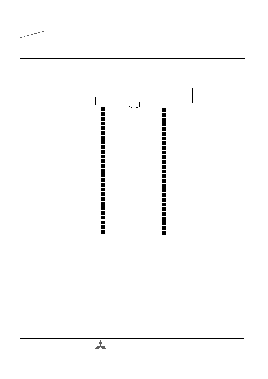
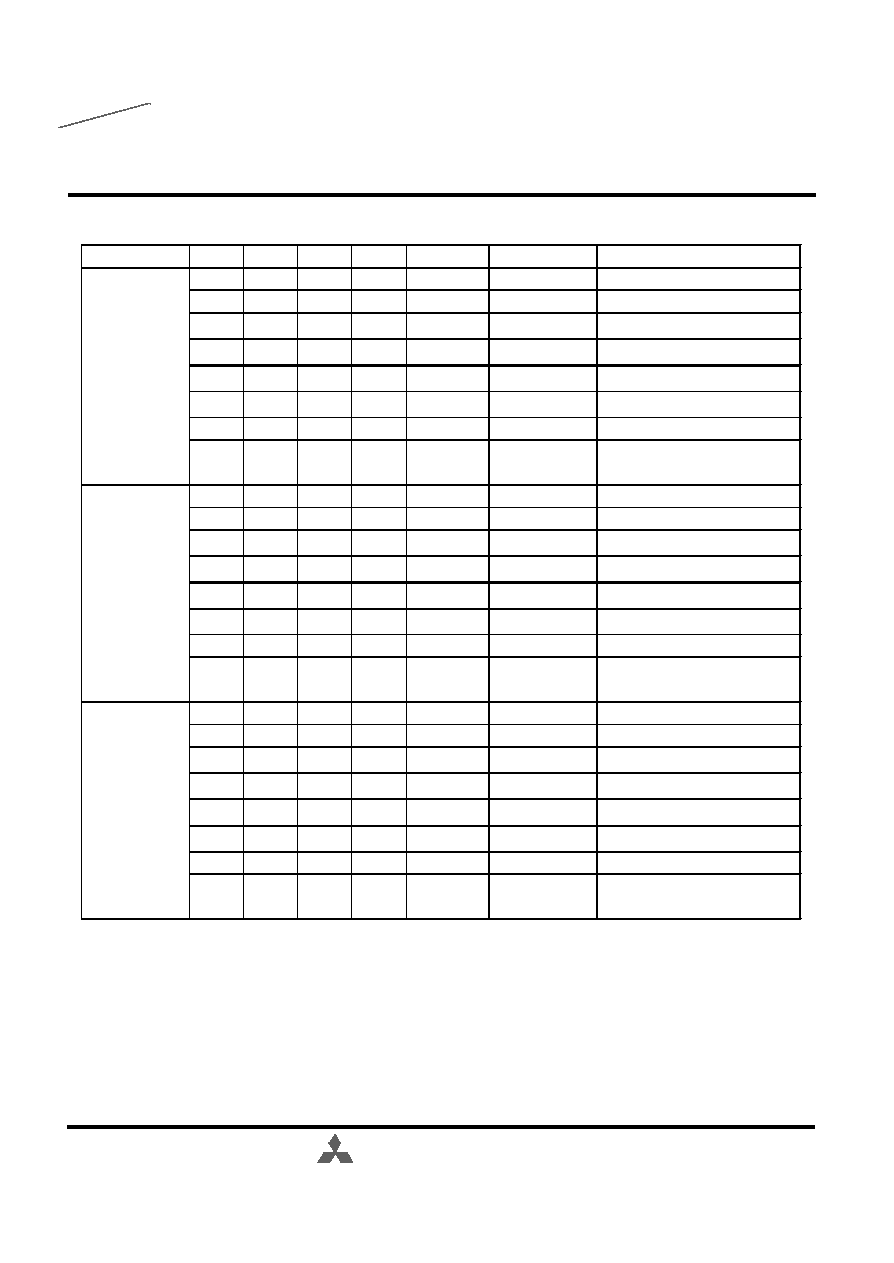
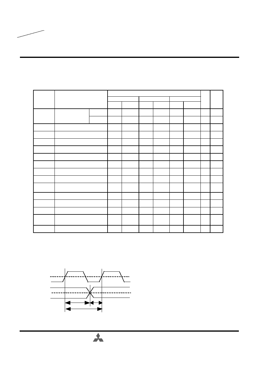
Vdd
NC
VddQ
NC
DQ0
VssQ
NC
NC
VddQ
NC
DQ1
VssQ
NC
Vdd
NC
/WE
/CAS
/RAS
/CS
BA0
BA1
A10/AP
A0
A1
A2
A3
Vdd
Vdd
DQ0
VddQ
NC
DQ1
VssQ
NC
DQ2
VddQ
NC
DQ3
VssQ
NC
Vdd
NC
/WE
/CAS
/RAS
/CS
BA0
BA1
A10/AP
A0
A1
A2
A3
Vdd
Vdd
DQ0
VddQ
DQ1
DQ2
VssQ
DQ3
DQ4
VddQ
DQ5
DQ6
VssQ
DQ7
Vdd
LDQM
/WE
/CAS
/RAS
/CS
BA0
BA1
A10/AP
A0
A1
A2
A3
Vdd
Vss
DQ15
VssQ
DQ14
DQ13
VddQ
DQ12
DQ11
VssQ
DQ10
DQ9
VddQ
DQ8
Vss
NC
UDQM
CLK
CKE
A12
A11
A9
A8
A7
A6
A5
A4
Vss
Vss
DQ7
VssQ
NC
DQ6
VddQ
NC
DQ5
VssQ
NC
DQ4
VddQ
NC
Vss
NC
DQM
CLK
CKE
A12
A11
A9
A8
A7
A6
A5
A4
Vss
Vss
NC
VssQ
NC
DQ3
VddQ
NC
NC
VssQ
NC
DQ2
VddQ
NC
Vss
NC
DQM
CLK
CKE
A12
A11
A9
A8
A7
A6
A5
A4
Vss
1
2
3
4
5
6
7
8
9
10
11
12
13
14
15
16
17
18
19
20
21
22
23
24
25
26
27
54
53
52
51
50
49
48
47
46
45
44
43
42
41
40
39
38
37
36
35
34
33
32
31
30
29
28
400
mil x 875mil 54pin 0.8mm pitch TSOP(II)
CLK
CKE
/CS
/RAS
/CAS
/WE
DQ0-15
DQM,DQMU/L
A0-12
BA0,1
Vdd
VddQ
Vss
VssQ
: Master Clock
: Clock Enable
: Chip Select
: Row Address Strobe
: Column Address Strobe
: Write Enable
: Data I/O
: Output Disable / Write Mask
: Address Input
: Bank Address Input
: Power Supply
: Power Supply for Output
: Ground
: Ground for Output
x4
x8
x16
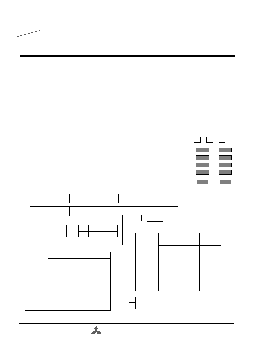
PIN CONFIGURATION
(TOP VIEW)
2
M2V56S20/ 30/ 40 TP ≠5,-5L, -6,-6L, -7,-7L
SDRAM (Rev.1.5E)
Single Data Rate
Oct.2001
256M Synchronous DRAM
MITSUBISHI LSIs
Preliminary
MITSUBISHI ELECTRIC
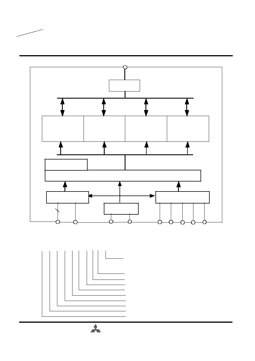
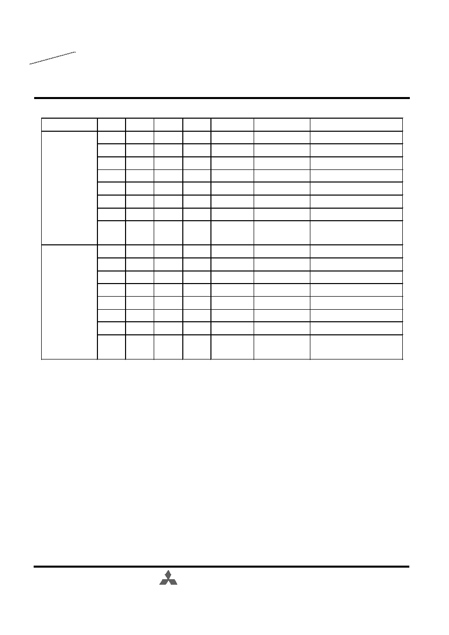
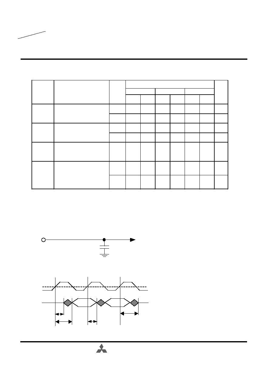
BLOCK DIAGRAM
DQ0-3 (x4), 0-7 (x8), 0-15 (x16)
I/O Buffer
Memory
Array
Bank #0
Memory
Array
Bank #1
Memory
Array
Bank #2
Memory
Array
Bank #3
Control Circuitry
Mode Register
Address Buffer
Clock Buffer
Control Signal Buffer
A0-12
BA0,1
CLK
CKE
/CS /RAS /CAS /WE DQMU/L
Speed Grade 5: 166MHz@CL3, 133MHz@CL2
6: 133MHz@CL3, 100MHz@CL2
7: 100MHz@CL2
Package Type TP: TSOP(II)
Process Generation
Function Reserved for Future Use
Organization 2
n
2:x4, 3:x8, 4:x16
SDRAM Data Rate Type S:Single Data Rate
Density 56: 256M bits
Interface V:LVTTL
Memory Style(DRAM)
Mitsubishi Main Designation
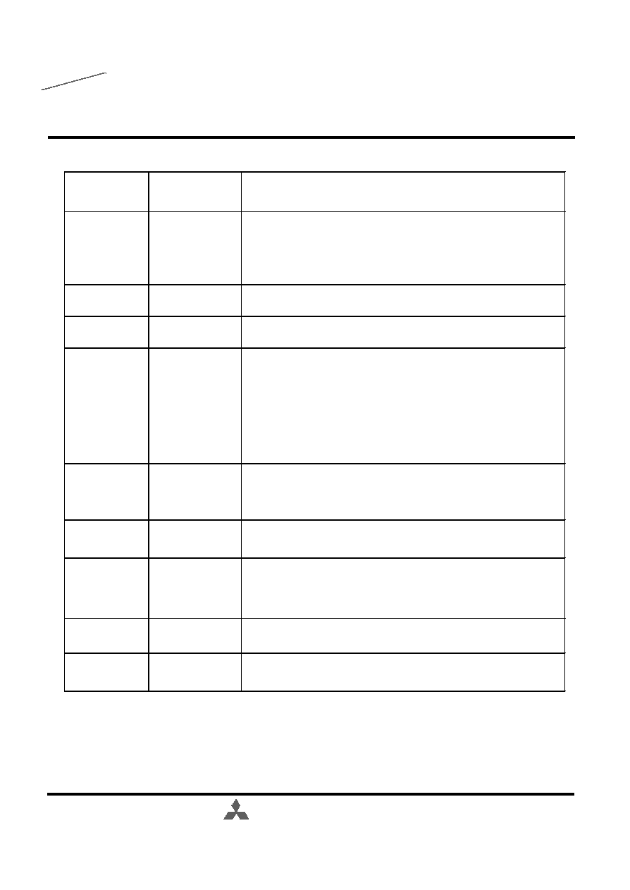
M 2 V 56 S 4
0 TP - 5
Type Designation Code
This rule is applied to only Synchronous DRAM family.
3
M2V56S20/ 30/ 40 TP ≠5,-5L, -6,-6L, -7,-7L
SDRAM (Rev.1.5E)
Single Data Rate
Oct.2001
256M Synchronous DRAM
MITSUBISHI LSIs
Preliminary
MITSUBISHI ELECTRIC
Master Clock: All other inputs are referenced to the rising edge of CLK.
Clock Enable: CKE controls internal clock. When CKE is low,internal
clock for the following cycle is ceased. CKE is also used to select auto
/self refresh. After self refresh mode is started. CKE becomes
asynchronous input. Self refresh is maintained as long as CKE is low.
A0-12 specify the Row/ Column Address in conjunction with BA0,1.
The Row Address is specified by A0-12.The Column Address is
specified by A0-9,11. A10 is also used to indicate precharge option.
When A10 is high at a read / write command, an auto precharge is
performed. When A10 is high at a precharge command, all banks are
precharged.
Bank Address : BA0,1 specifies one of four banks to which a command
is applied. BA0,1 must be set with ACT, PRE, READ, WRITE
commands.
Data In and Data out are referenced to the rising edge of CLK.
DQM
Din Mask / Output Disable: When DQMU/L is high in burst write, Din for
DQMU/L
Input
the current cycle is masked. When DQMU/L is high in burst read, Dout
is disabled at the next but one cycle.
Chip Select: When /CS is high, any command means No Operation
Combination of /RAS, /CAS, /WE defines basic commands.
Power supply for the memory array and peripheral circuitry.
VddQ and VssQ are supplied to the Output Buffers only.
Input
Input
Input
Input
A0-12
BA0,1
Power Supply
DQ0-15
Vdd,Vss
VddQ,VssQ
Input
Input
Input/Output
Power Supply
CLK
CKE
/CS
/RAS,/CAS,/WE
PIN FUNCTION
4
M2V56S20/ 30/ 40 TP ≠5,-5L, -6,-6L, -7,-7L
SDRAM (Rev.1.5E)
Single Data Rate
Oct.2001
256M Synchronous DRAM
MITSUBISHI LSIs
Preliminary
MITSUBISHI ELECTRIC
The M2V56S20/30/40TP provides basic functions, bank (row) activate, burst read / write, bank (row)
precharge, and auto / self refresh. Each command is defined by control signals of /RAS, /CAS and /WE at
CLK rising edge. In addition to 3 signals, /CS,CKE and A10 are used as chip select, refresh option, and
precharge option, respectively. To know the detailed definition of commands, please see the command
truth table.
BASIC FUNCTIONS
CLK
/CS
/RAS
/CAS
/WE
CKE
A10
Chip Select:L=select, H=deselect
Command
Command
Command
Refresh Option @refresh command
Precharge Option @ precharge or read/write command
define basic commands
Activate(ACT)[/RAS=L, /CAS=/WE=H]
ACT command activates a row in an idle bank indicated by BA.
Read(READ)[/RAS=H, /CAS=L, /WE=H]
READ command starts burst read from the active bank indicated by BA. First output data appears after
/CAS latency. When A10=H at this command, the bank is deactivated after the burst read (auto-
precharge,READA)
Write(WRITE[
/RAS=H, /CAS=L, /WE=L]
WRITE command starts burst write to the active bank indicated by BA. Total data length to be written
is set by burst length. When A10=H at this command, the bank is deactivated after the burst write
(auto-precharge, WRITEA).
Precharge(PRE)
[/RAS=L, /CAS=H, /WE=L]
PRE command deactivates the active bank indicated by BA. This command also terminates burst read
/write operation. When A10=H at this command, all banks are deactivated(precharge all, PREA).
Auto-Refresh(REFA)
[/RAS=/CAS=L, /WE=CKE=H]
REFA command starts auto-refresh cycle. Refresh address are generated internally.After this
command, the banks are precharged automatically.
5
M2V56S20/ 30/ 40 TP ≠5,-5L, -6,-6L, -7,-7L
SDRAM (Rev.1.5E)
Single Data Rate
Oct.2001
256M Synchronous DRAM
MITSUBISHI LSIs
Preliminary
MITSUBISHI ELECTRIC
CKE CKE
A10 A0-9,
n-1
n
/AP 11-12
Deselect
DESEL
H
X
H
X
X
X
X
X
X
No Operation
NOP
H
X
L
H
H
H
X
X
X
Row Address Entry&
Bank Activate
Single Bank Precharge
PRE
H
X
L
L
H
L
V
L
X
Precharge All Banks
PREA
H
X
L
L
H
L
X
H
X
Column Address Entry
&Write
Column Address Entry
&Write with
Auto-Precharge
Column Address Entry
&Read
Column Address Entry
&Read with
Auto-Precharge
Auto-Refresh
REFA
H
H
L
L
L
H
X
X
X
Self-Refresh Entry
REFS
H
L
L
L
L
H
X
X
X
L
H
H
X
X
X
X
X
X
L
H
L
H
H
H
X
X
X
Burst Terminate
TBST
H
X
L
H
H
L
X
X
X
Mode Register Set
MRS
H
X
L
L
L
L
L
L
V
1
COMMAND
MNEMONIC
/CS
/RAS /CAS /WE BA0,1
note
ACT
WRITE
WRITEA
H
X
L
L
H
H
READ
READA
Self-Refresh Exit
REFSX
H
X
L
H
L
V
V
V
L
V
L
V
H
X
L
H
L
L
V
H
V
H
X
L
H
L
H
V
L
V
H
X
L
H
V
L
H
V
H
COMMAND TRUTH TABLE
H=High Level, L=Low Level, V=Valid, X=Don't Care, n=CLK cycle number
NOTE:
1. A7-9, 11-12=L, A0-A6 =Mode Address
6
M2V56S20/ 30/ 40 TP ≠5,-5L, -6,-6L, -7,-7L
SDRAM (Rev.1.5E)
Single Data Rate
Oct.2001
256M Synchronous DRAM
MITSUBISHI LSIs
Preliminary
MITSUBISHI ELECTRIC
FUNCTION TRUTH TABLE
7
Current State /CS /RAS /CAS /WE
Address
Command
Action
IDLE
H
X
X
X
X
DESEL
NOP
L
H
H
H
X
NOP
NOP
L
H
H
L
X
TBST
ILLEGAL
*
2
L
H
L
X
BA,CA,A10 READ/WRITE ILLEGAL
*
2
L
L
H
H
BA,RA
ACT
Bank Active,Latch RA
L
L
H
L
BA,A10
PRE/PREA
NOP
*
4
L
L
L
H
X
REFA
Auto-Refresh
*
5
Op-Code,
Mode-Add
ROW ACTIVE
H
X
X
X
X
DESEL
NOP
L
H
H
H
X
NOP
NOP
L
H
H
L
X
TBST
NOP
Begin Read,Latch CA,
Determine Auto-Precharge
WRITE/
Begin Write,Latch CA,
WRITEA
Determine Auto-Precharge
L
L
H
H
BA,RA
ACT
Bank Active/ILLEGAL
*
2
L
L
H
L
BA,A10
PRE/PREA
Precharge/Precharge All
L
L
L
H
X
REFA
ILLEGAL
Op-Code,
Mode-Add
READ
H
X
X
X
X
DESEL
NOP(Continue Burst to END)
L
H
H
H
X
NOP
NOP(Continue Burst to END)
L
H
H
L
X
TBST
Terminate Burst
Terminate Burst,Latch CA,
Begin New Read,Determine
Auto-Precharge
*
3
Terminate Burst,Latch CA,
WRITE/WRITEA Begin Write,Determine
Auto-Precharge
*
3
L
L
H
H
BA,RA
ACT
Bank Active/ILLEGAL
*
2
L
L
H
L
BA,A10
PRE/PREA
Terminate Burst,Precharge
L
L
L
H
X
REFA
ILLEGAL
Op-Code,
Mode-Add
MRS
Mode Register Set
*
5
BA,CA,A10 READ/READA
L
L
L
H
L
H
L
L
BA,CA,A10
L
L
L
L
L
H
L
L
L
MRS
ILLEGAL
L
H
L
H
BA,CA,A10 READ/READA
ILLEGAL
BA,CA,A10
L
L
L
L
MRS
L
H
L
M2V56S20/ 30/ 40 TP ≠5,-5L, -6,-6L, -7,-7L
SDRAM (Rev.1.5E)
Single Data Rate
Oct.2001
256M Synchronous DRAM
MITSUBISHI LSIs
Preliminary
MITSUBISHI ELECTRIC
Current State
/CS
/RAS /CAS
/WE
Address
Command
Action
WRITE
H
X
X
X
X
DESEL
NOP(Continue Burst to END)
L
H
H
H
X
NOP
NOP(Continue Burst to END)
L
H
H
L
X
TBST
Terminate Burst
Terminate Burst,Latch CA,
Begin Read,Determine
Auto-Precharge
*
3
Terminate Burst,Latch CA,
WRITE/
Begin Write,Determine
WRITEA
Auto-Precharge
*
3
L
L
H
H
BA,RA
ACT
Bank Active/ILLEGAL
*
2
L
L
H
L
BA,A10
PRE/PREA Terminate Burst,Precharge
L
L
L
H
X
REFA
ILLEGAL
Op-Code,
Mode-Add
READ with
H
X
X
X
X
DESEL
NOP(Continue Burst to END)
AUTO
L
H
H
H
X
NOP
NOP(Continue Burst to END)
PRECHARGE
L
H
H
L
X
TBST
ILLEGAL
L
H
L
H
BA,CA,A10 READ/READA ILLEGAL
WRITE/
WRITEA
L
L
H
H
BA,RA
ACT
Bank Active/ILLEGAL
*
2
L
L
H
L
BA,A10
PRE/PREA ILLEGAL
*
2
L
L
L
H
X
REFA
ILLEGAL
Op-Code,
Mode-Add
WRITE with
H
X
X
X
X
DESEL
NOP(Continue Burst to END)
AUTO
L
H
H
H
X
NOP
NOP(Continue Burst to END)
PRECHARGE
L
H
H
L
X
TBST
ILLEGAL
L
H
L
H
BA,CA,A10 READ/READA ILLEGAL
WRITE/
WRITEA
L
L
H
H
BA,RA
ACT
Bank Active/ILLEGAL
*
2
L
L
H
L
BA,A10
PRE/PREA ILLEGAL
*
2
L
L
L
H
X
REFA
ILLEGAL
Op-Code,
Mode-Add
BA,CA,A10
ILLEGAL
L
H
L
L
H
L
L
L
L
L
BA,CA,A10
ILLEGAL
MRS
ILLEGAL
MRS
BA,CA,A10 READ/READA
L
H
L
H
L
H
L
L
L
L
L
L
L
ILLEGAL
L
L
L
L
MRS
BA,CA,A10
ILLEGAL
L
FUNCTION TRUTH TABLE (continued)
8
M2V56S20/ 30/ 40 TP ≠5,-5L, -6,-6L, -7,-7L
SDRAM (Rev.1.5E)
Single Data Rate
Oct.2001
256M Synchronous DRAM
MITSUBISHI LSIs
Preliminary
MITSUBISHI ELECTRIC
Current State
/CS
/RAS /CAS
/WE
Address
Command
Action
PRE-
H
X
X
X
X
DESEL
NOP(Idle after tRP)
CHARGING
L
H
H
H
X
NOP
NOP(Idle after tRP)
L
H
H
L
X
TBST
ILLEGAL
*
2
L
H
L
X
BA,CA,A10 READ/WRITE ILLEGAL
*
2
L
L
H
H
BA,RA
ACT
ILLEGAL
*
2
L
L
H
L
BA,A10
PRE/PREA NOP
*
4(Idle after tRP)
L
L
L
H
X
REFA
ILLEGAL
Op-Code,
Mode-Add
ROW
H
X
X
X
X
DESEL
NOP(Row active after tRCD)
ACTIVATING
L
H
H
H
X
NOP
NOP(Row active after tRCD)
L
H
H
L
X
TBST
ILLEGAL
*
2
L
H
L
X
BA,CA,A10 READ/WRITE ILLEGAL
*
2
L
L
H
H
BA,RA
ACT
ILLEGAL
*
2
L
L
H
L
BA,A10
PRE/PREA ILLEGAL
*
2
L
L
L
H
X
REFA
ILLEGAL
Op-Code,
Mode-Add
WRITE RE-
H
X
X
X
X
DESEL
NOP
COVERING
L
H
H
H
X
NOP
NOP
L
H
H
L
X
TBST
ILLEGAL
*
2
L
H
L
X
BA,CA,A10 READ/WRITE ILLEGAL
*
2
L
L
H
H
BA,RA
ACT
ILLEGAL
*
2
L
L
H
L
BA,A10
PRE/PREA ILLEGAL
*
2
L
L
L
H
X
REFA
ILLEGAL
Op-Code,
Mode-Add
ILLEGAL
MRS
ILLEGAL
L
L
L
L
MRS
MRS
ILLEGAL
L
L
L
L
L
L
L
L
FUNCTION TRUTH TABLE (continued)
9
M2V56S20/ 30/ 40 TP ≠5,-5L, -6,-6L, -7,-7L
SDRAM (Rev.1.5E)
Single Data Rate
Oct.2001
256M Synchronous DRAM
MITSUBISHI LSIs
Preliminary
MITSUBISHI ELECTRIC
Current State /CS
/RAS /CAS /WE
Address
Command
Action
RE-
H
X
X
X
X
DESEL
NOP(Idle after tRFC)
FRESHING
L
H
H
H
X
NOP
NOP(Idle after tRFC)
L
H
H
L
X
TBST
ILLEGAL
L
H
L
X
BA,CA,A10 READ/WRITE ILLEGAL
L
L
H
H
BA,RA
ACT
ILLEGAL
L
L
H
L
BA,A10
PRE/PREA ILLEGAL
L
L
L
H
X
REFA
ILLEGAL
Op-Code,
Mode-Add
MODE
H
X
X
X
X
DESEL
NOP(Idle after tRSC)
REGISTER
L
H
H
H
X
NOP
NOP(Idle after tRSC)
SETTING
L
H
H
L
X
TBST
ILLEGAL
L
H
L
X
BA,CA,A10 READ/WRITE ILLEGAL
L
L
H
H
BA,RA
ACT
ILLEGAL
L
L
H
L
BA,A10
PRE/PREA ILLEGAL
L
L
L
H
X
REFA
ILLEGAL
Op-Code,
Mode-Add
ILLEGAL
MRS
MRS
ILLEGAL
L
L
L
L
L
L
L
L
FUNCTION TRUTH TABLE (continued)
ABBREVIATIONS:
H=High Level, L=Low Level, X=Don't Care
BA=Bank Address, RA=Row Address, CA=Column Address, NOP=No OPeration
NOTES:
1.All entries assume that CKE was High during the preceding clock cycle and the current clock cycle.
2.ILLEGAL to bank in specified states ; function may be legal in the bank indicated by BA, depending on the
state that bank.
3.Must satisfy bus contention, bus turn around, write recovery requirements.
4.NOP to bank precharging or in idle state. May precharge bank indicated by BA.
5.ILLEGAL if any bank is not idle.
ILLEGAL=Device operation and/or data-integrity are not guaranteed.
10
M2V56S20/ 30/ 40 TP ≠5,-5L, -6,-6L, -7,-7L
SDRAM (Rev.1.5E)
Single Data Rate
Oct.2001
256M Synchronous DRAM
MITSUBISHI LSIs
Preliminary
MITSUBISHI ELECTRIC
CKE CKE
n-1
n
SELF-
H
X
X
X
X
X
X INVALID
REFRESH
*
1
L
H
H
X
X
X
X Exit Self-Refresh(Idle after tRC)
L
H
L
H
H
H
X Exit Self-Refresh(Idle after tRC)
L
H
L
H
H
L
X ILLEGAL
L
H
L
H
L
X
X ILLEGAL
L
H
L
L
X
X
X ILLEGAL
L
L
X
X
X
X
X NOP(Maintain Self-Refresh)
POWER
H
X
X
X
X
X
X INVALID
DOWN
L
H
X
X
X
X
X Exit Power Down to Idle
L
L
X
X
X
X
X NOP(Maintain Power Down)
ALL BANKS
H
H
X
X
X
X
X Refer to Function Truth Table
IDLE
*
2
H
L
L
L
L
H
X Enter Self-Refresh
H
L
H
X
X
X
X Enter Power Down
H
L
L
H
H
H
X Enter Power Down
H
L
L
H
H
L
X ILLEGAL
H
L
L
H
L
X
X ILLEGAL
H
L
L
L
X
X
X ILLEGAL
L
X
X
X
X
X
X Refer to Current State=Power Down
ANY STATE
H
H
X
X
X
X
X Refer to Function Truth Table
other than
H
L
X
X
X
X
X Begin CLK Suspend at Next Cycle
*
3
listed above
L
H
X
X
X
X
X Exit CLK Suspend at Next Cycle
*
3
L
L
X
X
X
X
X Maintain CLK Suspend
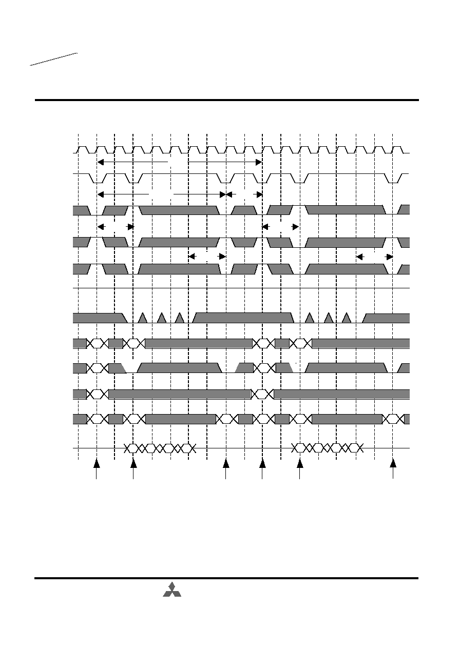
/WE Add
Current State
Action
/CS /RAS /CAS
ABBREVIATIONS:
H=High Level, L=Low Level, X=Don't Care
NOTES:
1.CKE Low to High transition will re-enable CLK and other inputs asynchronously.
A minimum set up time must be satisfied before any command other than EXIT.
2.Self-Refresh can be entered only from the All Banks ldle State.
3.Must be legal command.
FUNCTION TRUTH TABLE For CKE
11
M2V56S20/ 30/ 40 TP ≠5,-5L, -6,-6L, -7,-7L
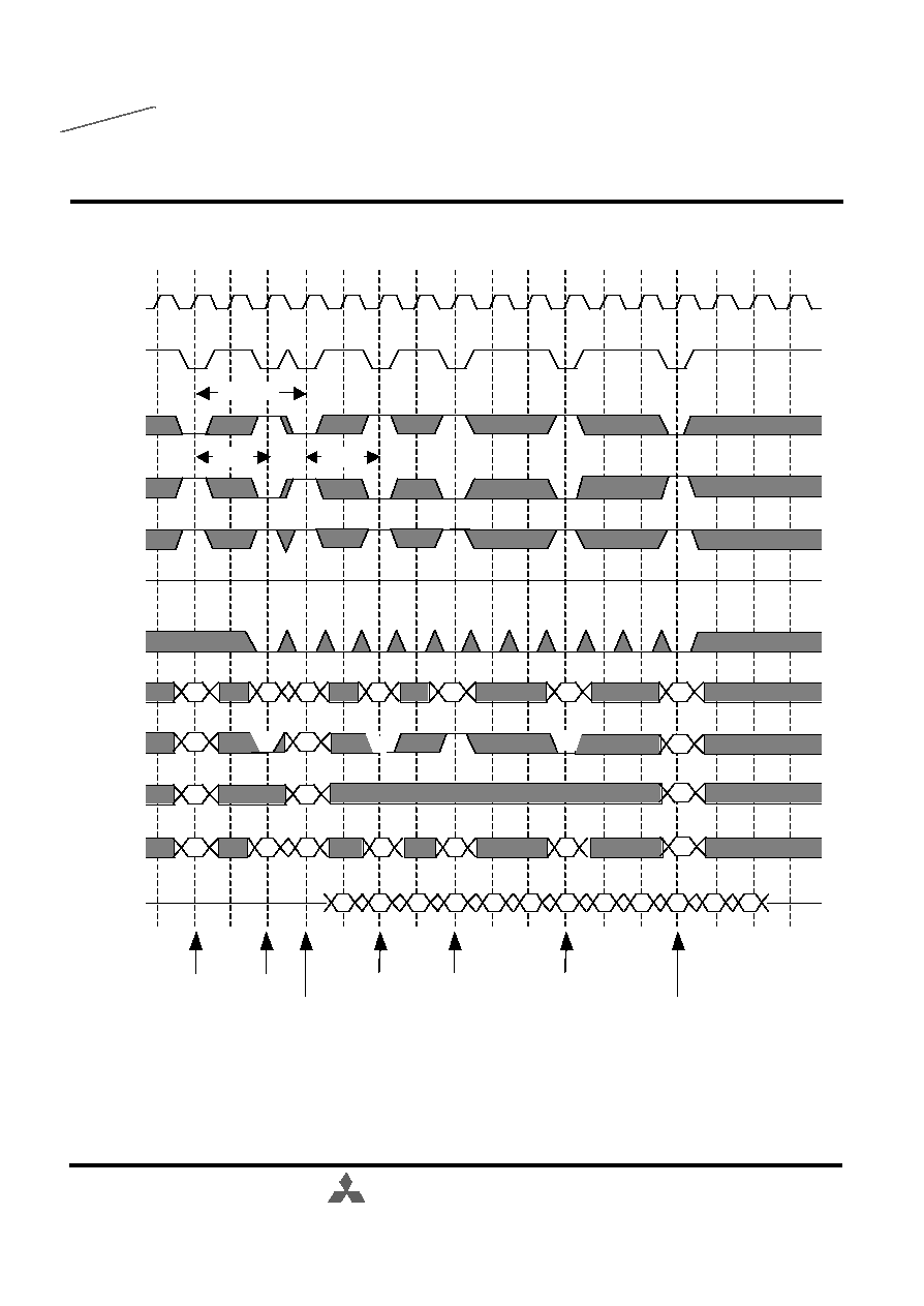
SDRAM (Rev.1.5E)
Single Data Rate
Oct.2001
256M Synchronous DRAM
MITSUBISHI LSIs
Preliminary
MITSUBISHI ELECTRIC
WRITE
POWER
ON
PRE
CHARGE
PRE
POWER
APPLIED
WRITEA
SUSPEND
WRITEA
CKEL
CKEH
PRE
PRE
PRE
READA
SUSPEND
READA
CKEL
CKEH
WRITEA
READA
WRITEA
READA
READ
SUSPEND
CKEL
CKEH
READ
READ
WRITE
WRITE
SUSPEND
CKEL
CKEH
READ
WRITE
READA
WRITEA
ROW
ACTIVE
TBST
SELF
REFRESH
AUTO
REFRESH
CLK
SUSPEND
IDLE
POWER
DOWN
MODE
REGISTER
SET
MRS
REFA
CKEL
CKEH
ACT
CKEL
CKEH
REFSX
REFS
TBST
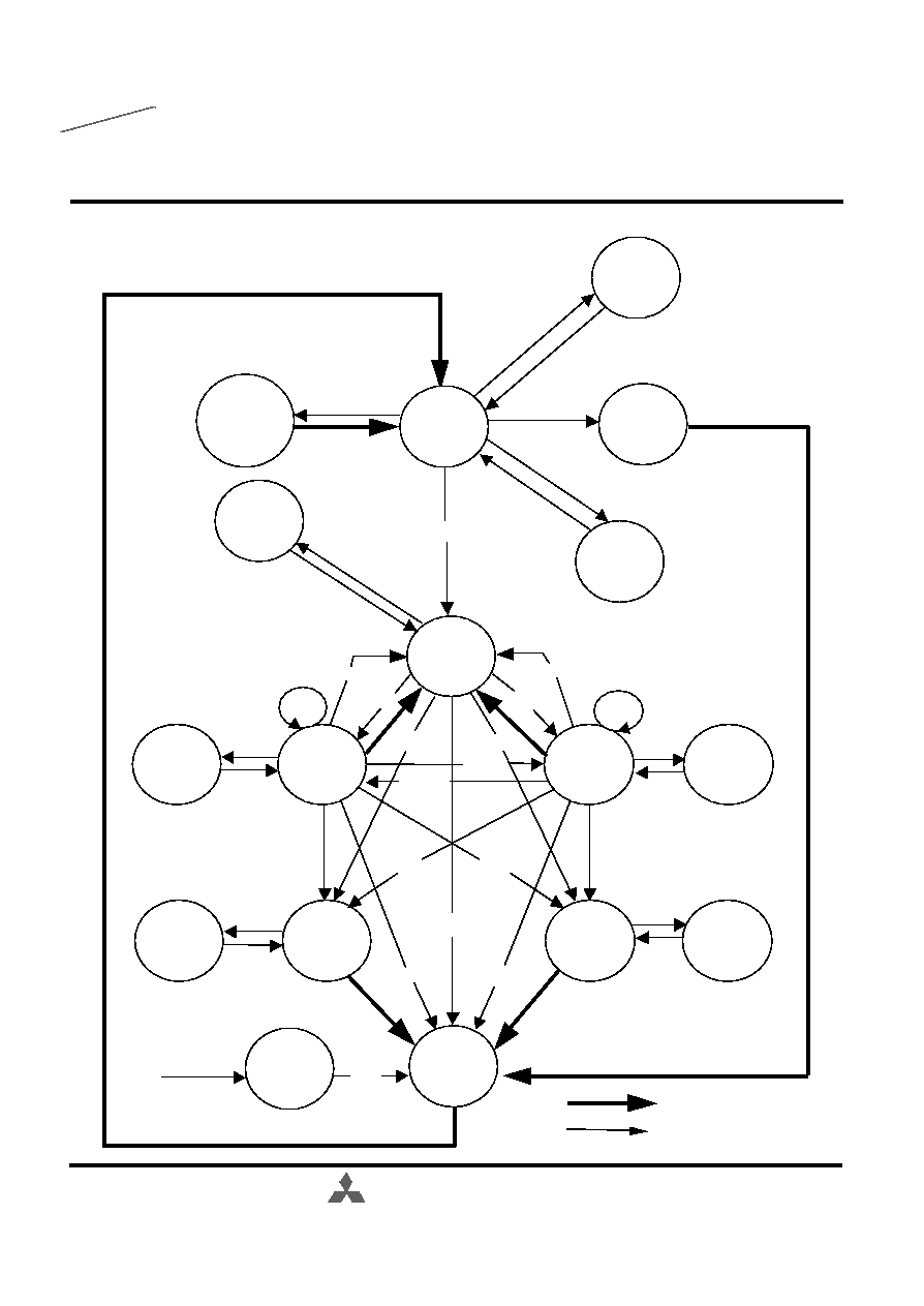
Automatic Sequence
Command Sequence
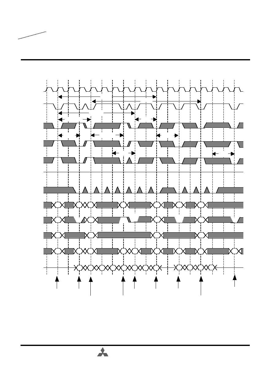
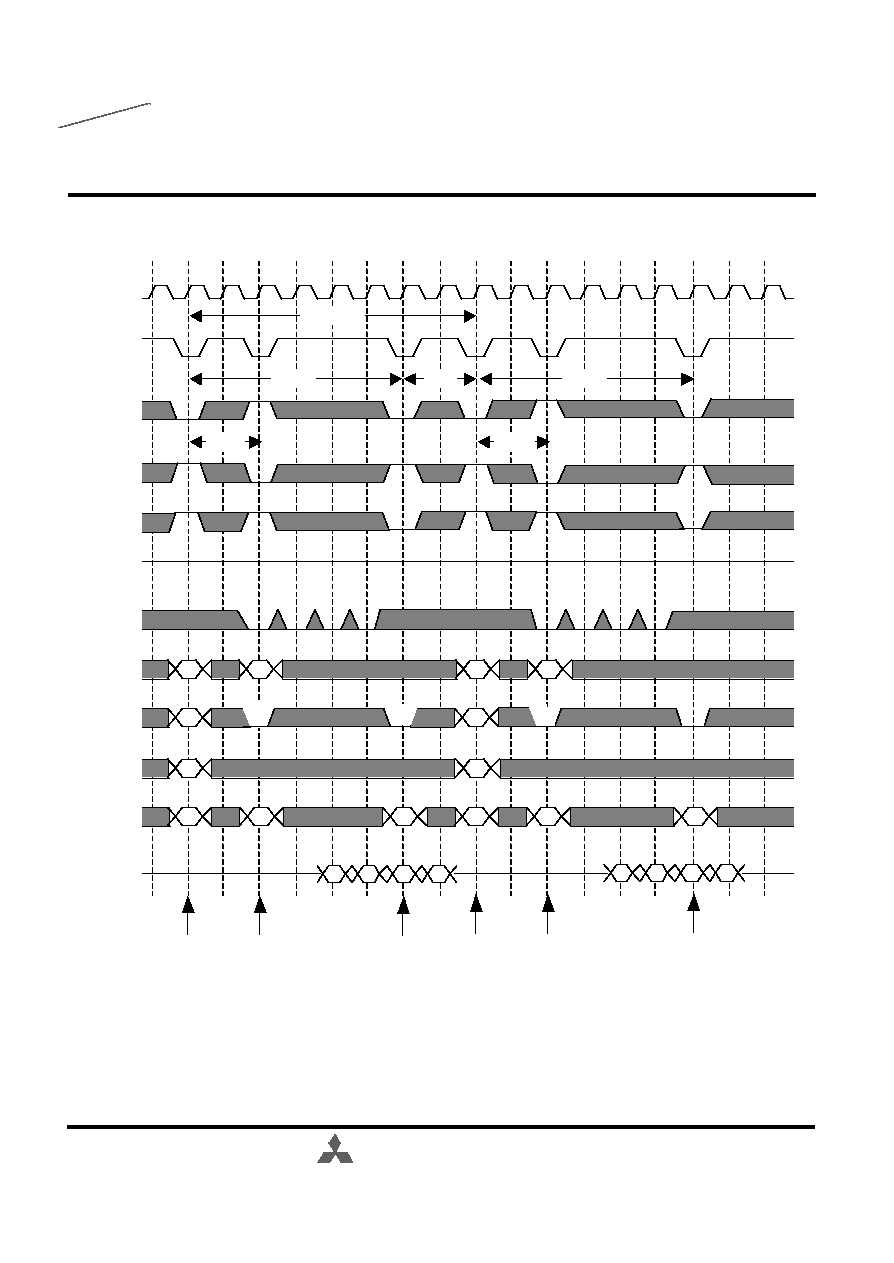
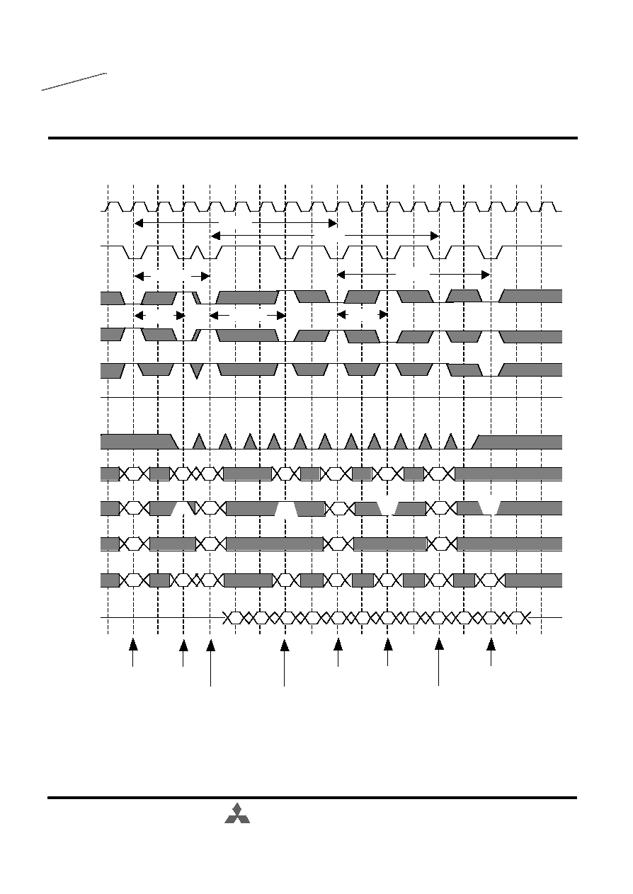
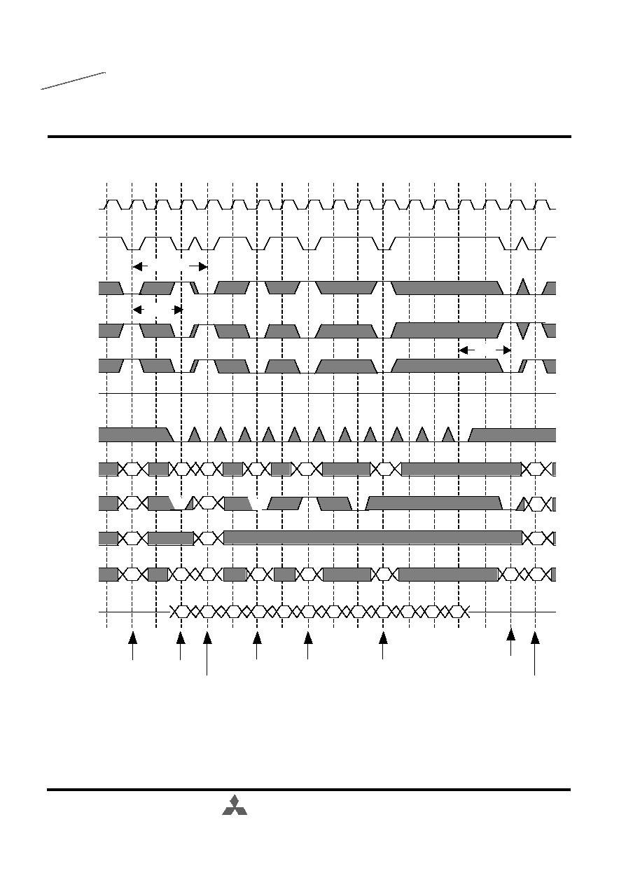
SIMPLIFIED STATE DIAGRAM
12
M2V56S20/ 30/ 40 TP ≠5,-5L, -6,-6L, -7,-7L
SDRAM (Rev.1.5E)
Single Data Rate
Oct.2001
256M Synchronous DRAM
MITSUBISHI LSIs
Preliminary
MITSUBISHI ELECTRIC
Before starting normal operation, the following power on sequence is necessary to prevent a
SDRAM from damaged or malfunctioning.
1. Apply power and start clock. Attempt to maintain CKE high, DQM high and NOP condition at the
inputs.
2. Maintain stable power, stable clock, and NOP input conditions for a minimum of 100µs.
3. Issue precharge commands for all banks. (PRE or PREA)
4. After all banks become idle state (after tRP), issue 2 or more auto-refresh commands.
5. Issue a mode register set command to initialize the mode register.
After these sequence, the SDRAM is idle state and ready for normal operation.
Burst Length, Burst Type and /CAS Latency can be programmed by
setting the mode register (MRS). The mode register stores these data
until the next MRS command, which may be issued when all banks are in
idle state. After tRSC from a MRS command, the SDRAM is ready for
new command.
POWER ON SEQUENCE
MODE REGISTER
CLK
/CS
/RAS
/CAS
/WE
BA0, 1 A12-A0
V
BA0 BA1 A12 A11 A10 A9 A8 A7 A6 A5 A4 A3
A2
A1
A0
0
0
0
0
0
SW
0
0
BT
LTMODE
BL
1
SEQUENTIAL
INTERLEAVED
0
BURST
TYPE
LATENCY
MODE
CL
0 0 0
0 0 1
0 1 0
0 1 1
1 0 0
1 0 1
1 1 0
1 1 1
/CAS LATENCY
R
R
2
3
R
R
R
R
BURST
LENGTH
BL
0 0 0
0 0 1
0 1 0
0 1 1
1 0 0
1 0 1
1 1 0
1 1 1
BT=0
1
2
4
8
R
R
R
Full Page
BT=1
1
2
4
8
R
R
R
R
1
Burst Write
Single Write
0
SW
13
R:Reserved for Future Use

M2V56S20/ 30/ 40 TP ≠5,-5L, -6,-6L, -7,-7L
SDRAM (Rev.1.5E)
Single Data Rate
Oct.2001
256M Synchronous DRAM
MITSUBISHI LSIs
Preliminary
MITSUBISHI ELECTRIC
Burst Type
Q0
Q1
Q2
Q3
D0
D1
D2
D3
Burst Length
Burst Length
Write
CLK
Command
Address
CL=3
BL=4
/CAS=Latency
Read
Y
Y
DQ
14
BL
A2
A1
A0
0
0
0
0
1
2
3
4
5
6
7
0
1
2
3
4
5
6
7
0
0
1
1
2
3
4
5
6
7
0
1
0
3
2
5
4
7
6
0
1
0
2
3
4
5
6
7
0
1
2
3
0
1
6
7
4
5
0
1
1
3
4
5
6
7
0
1
2
3
2
1
0
7
6
5
4
1
0
0
4
5
6
7
0
1
2
3
4
5
6
7
0
1
2
3
1
0
1
5
6
7
0
1
2
3
4
5
4
7
6
1
0
3
2
1
1
0
6
7
0
1
2
3
4
5
6
7
4
5
2
3
0
1
1
1
1
7
0
1
2
3
4
5
6
7
6
5
4
3
2
1
0
-
0
0
0
1
2
3
0
1
2
3
-
0
1
1
2
3
0
1
0
3
2
-
1
0
2
3
0
1
2
3
0
1
-
1
1
3
0
1
2
3
2
1
0
-
-
0
0
1
0
1
-
-
1
1
0
1
0
4
2
Initial Address
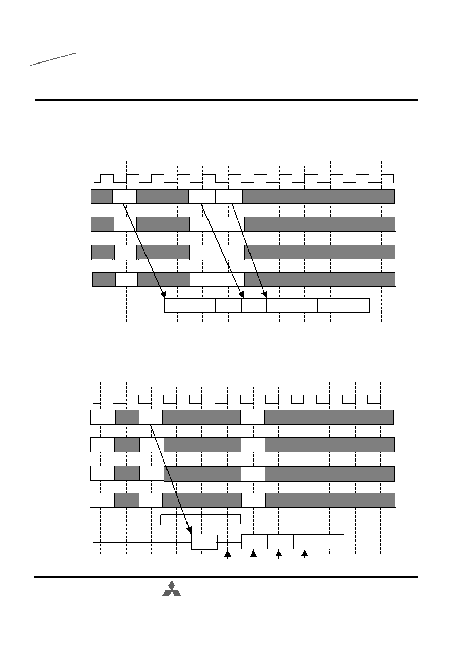
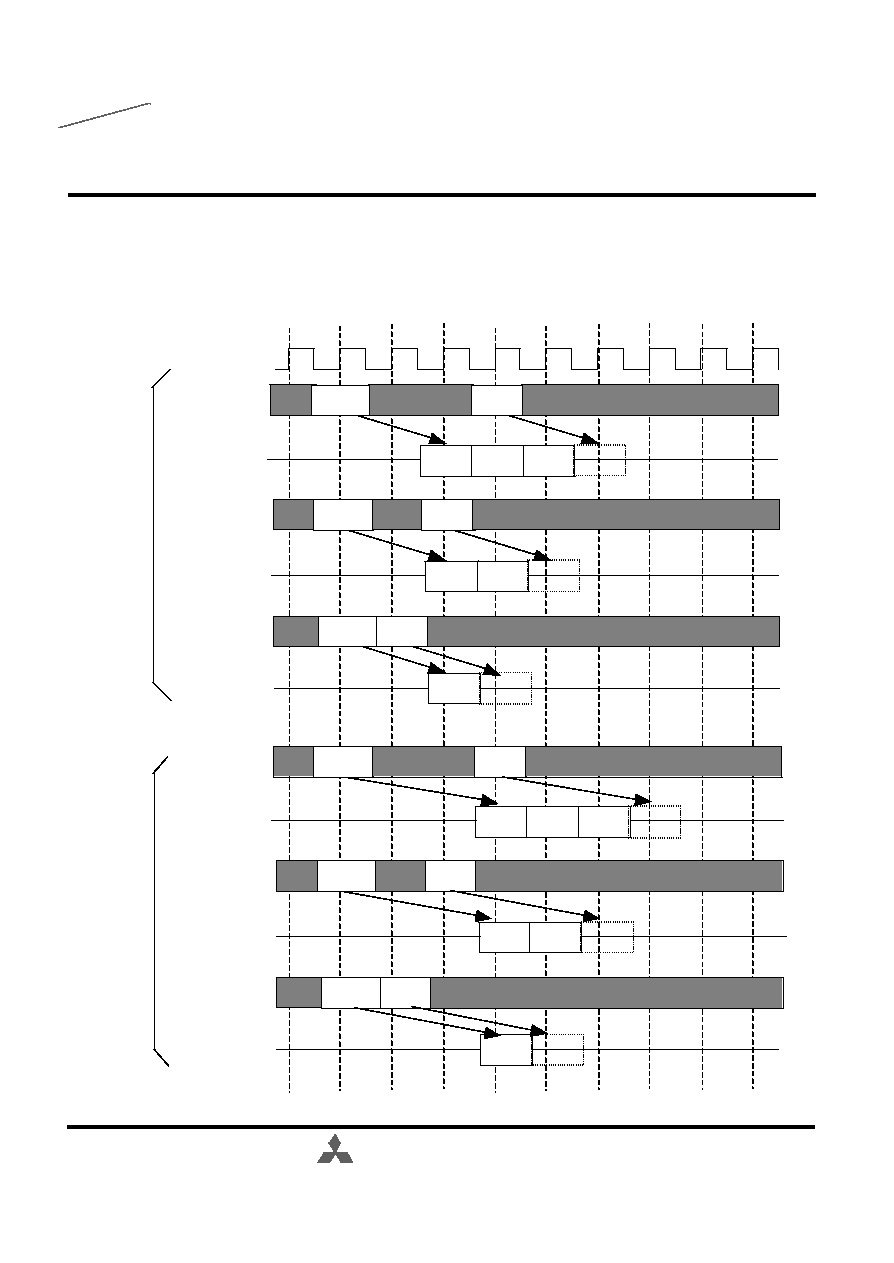
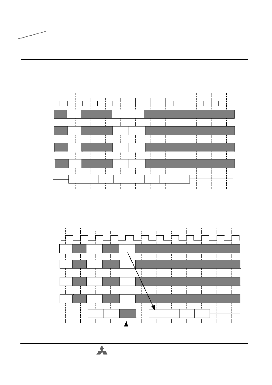
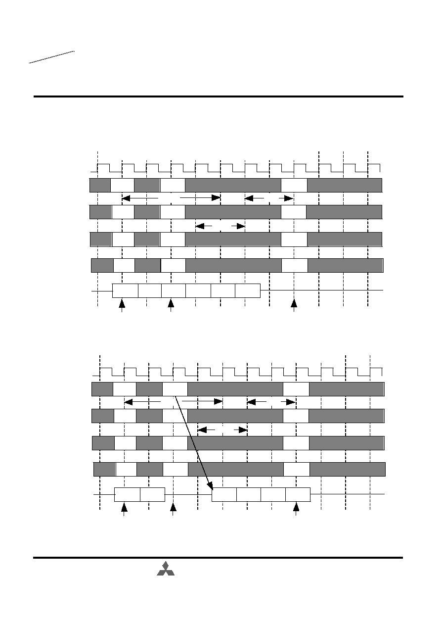
Column Addressing
Sequential
Interleaved
8
M2V56S20/ 30/ 40 TP ≠5,-5L, -6,-6L, -7,-7L
SDRAM (Rev.1.5E)
Single Data Rate
Oct.2001
256M Synchronous DRAM
MITSUBISHI LSIs
Preliminary
MITSUBISHI ELECTRIC
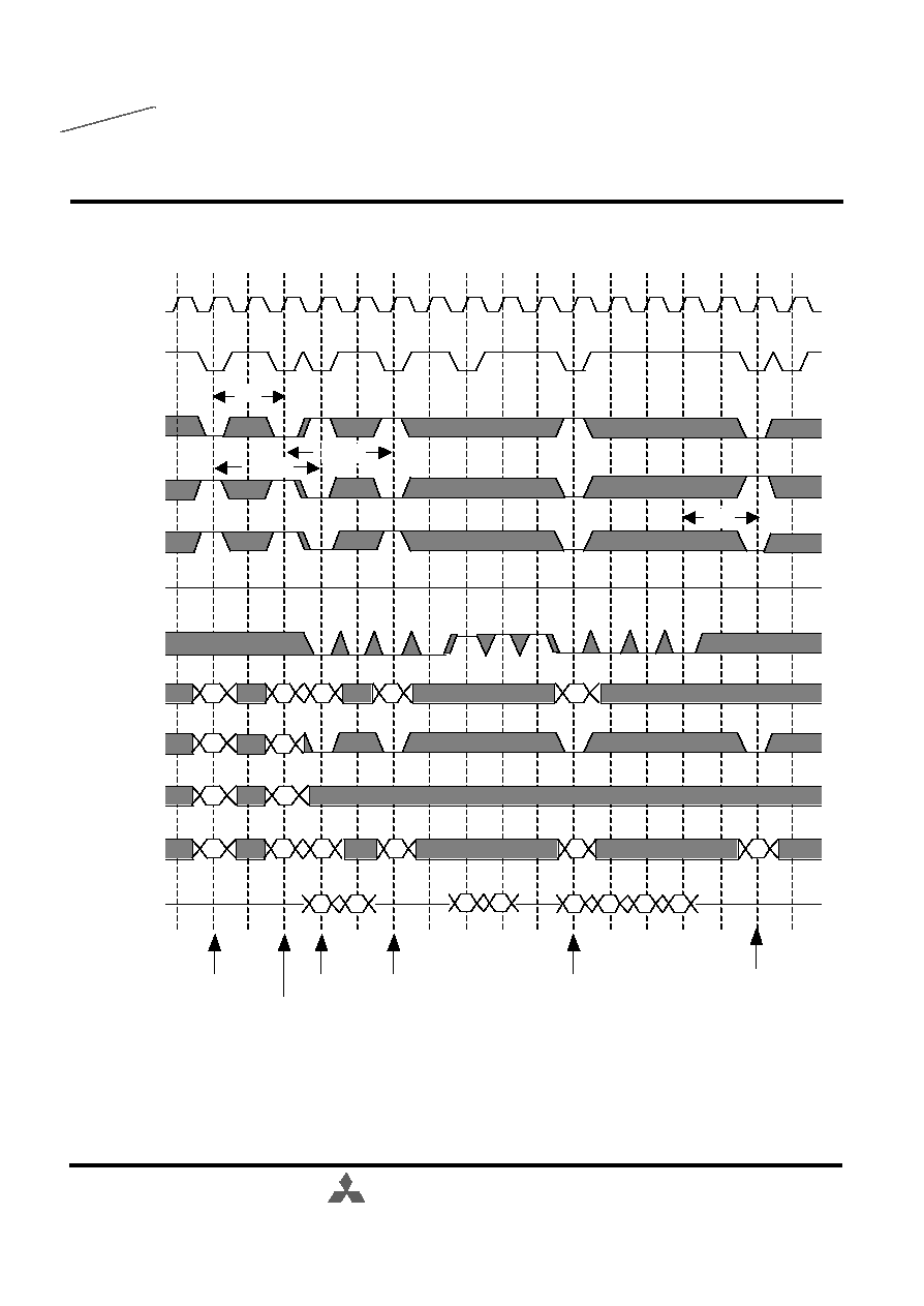
BANK ACTIVATE
One of four banks is activated by an ACT command.
An bank is selected by BA0-1. A row is selected by A0-12.
Multiple banks can be active state concurrently by issuing multiple ACT commands.
Minimum activation interval between one bank and another bank is tRRD.
PRECHARGE
An open bank is deactivated by a PRE command.
A bank to be deactivated is designated by BA0-1.
When multiple banks are active, a precharge all command (PREA, PRE + A10=H) deactivates all of
open banks at the same time. BA0-1 are "Don't Care" in this case.
Minimum delay time of an ACT command after a PRE command to the same bank is tRP.
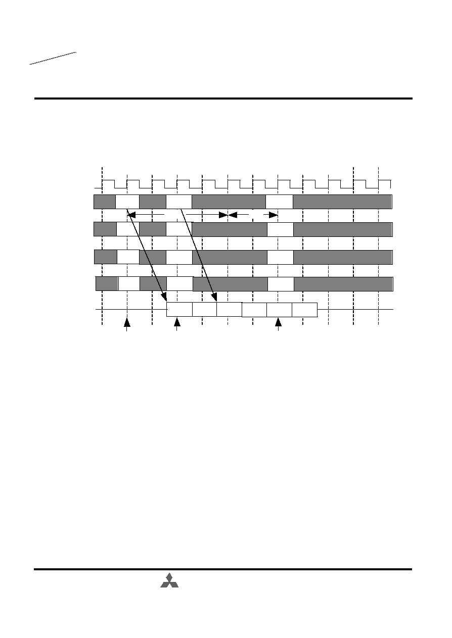
OPERATIONAL DESCRIPTION
CLK
Command
Bank Activation and Precharge All (BL=4, CL=3)
tRCD
ACT
ACT
READ
ACT
PRE
Xa
Xb
Yb
Xa
Xa
Xb
Xa
0
01
1
00
01
Qb0
Qb1
Qb2
Qb3
A0-9,11-12
A10
BA0-1
DQ
Precharge All
tRP
READ
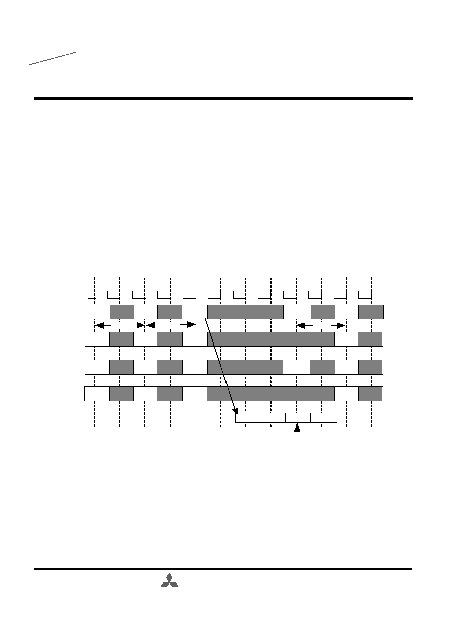
A READ command can be issued to any active bank. The start address is specified by A0-9,11(x4),A0-
9 (x8), A0-8 (x16). 1st output data is available after the /CAS Latency from the READ. The consecutive
data length is defined by the Burst Length .The address sequence of the burst data is defined by the Burst
Type. Minimum delay time of a READ command after an ACT command to the same bank is tRCD.
When A10 is high at a READ command, auto-precharge (READA) is performed. Any command (READ,
WRITE, PRE, ACT, TBST) to the same bank is inhibited till the internal precharge is complete.The
Internal precharge starts at the BL after READA. The next ACT command can be issued after (BL +
tRP) from the previous READA. In any case, tRCD+BL > tRASmin must be met.
15
00
tRRD
M2V56S20/ 30/ 40 TP ≠5,-5L, -6,-6L, -7,-7L
SDRAM (Rev.1.5E)
Single Data Rate
Oct.2001
256M Synchronous DRAM
MITSUBISHI LSIs
Preliminary
MITSUBISHI ELECTRIC
16
CLK
Command
ACT
READ
ACT
ACT
PRE
Xa
Ya
Xb
Xa
Xa
0
Xa
Xb
01
00
00
00
A0-9,11-12
A10
BA0-1
DQ
tRP
Yb
0
0
00
01
Qa0
Qa1
Qa2
Qa3
Qb0
Qb1
Qb2
Qb3
READ
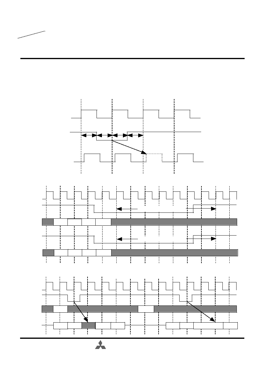
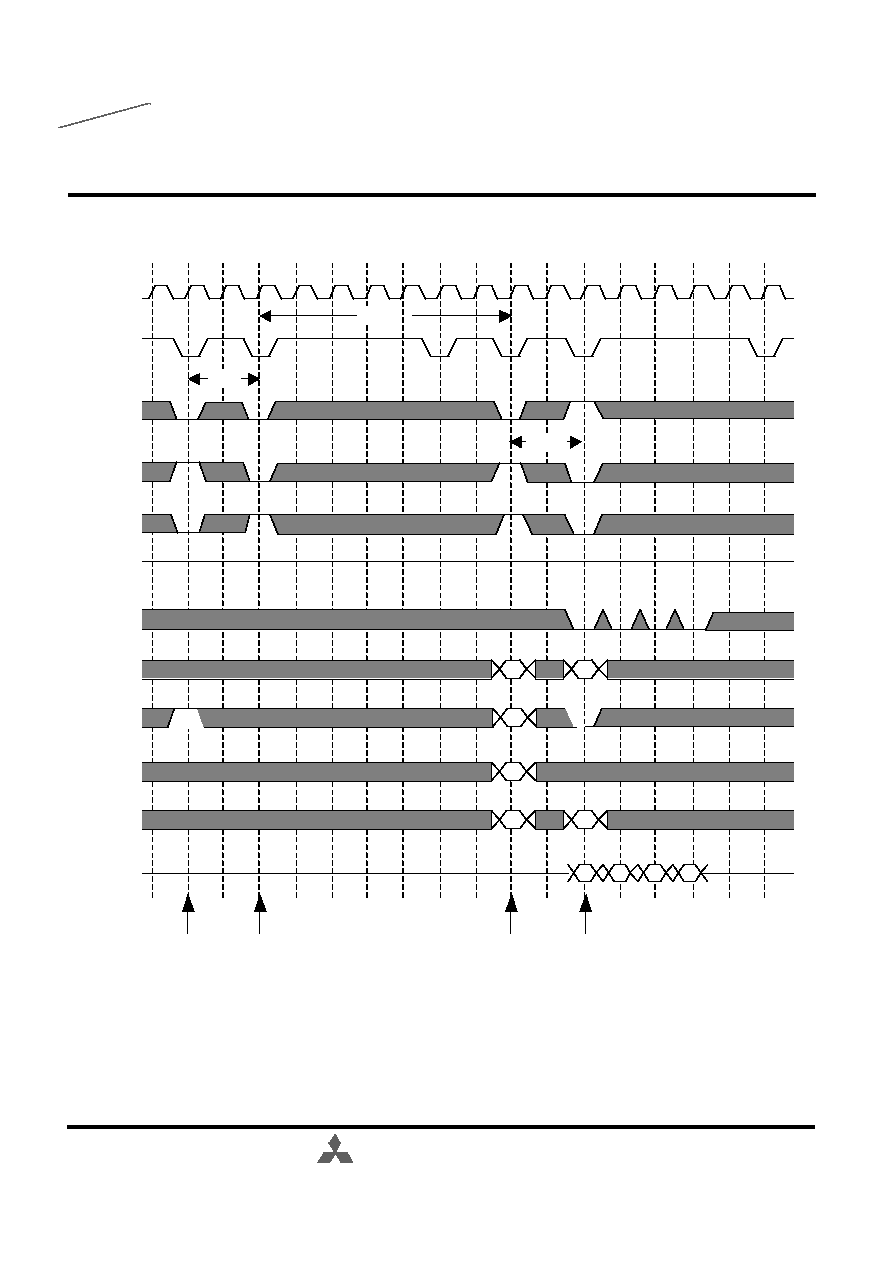
Multi Bank Interleaving Read (CL=2, BL=4)
ACT
READ
ACT
Qa0 Qa1
Qa2
Qa3
Qa0 Qa1
Qa2
Qa3
Internal precharge starts
CL=2
CL=3
CLK
Command
DQ
DQ
tRCD
tRP
BL
ACT
READ
ACT
Xa
Ya
Xa
Xa
1
Xa
00
00
00
CLK
Command
A0-9,11-12
A10
BA0-1
DQ
Internal precharge starts
Qa0
Qa1
Qa2
Qa3
Read with Auto-Precharge (CL=2, BL=4)
Auto-Precharge Timing (READ, BL=4)
tRCD
BL
tRCD
tRCD
M2V56S20/ 30/ 40 TP ≠5,-5L, -6,-6L, -7,-7L
SDRAM (Rev.1.5E)
Single Data Rate
Oct.2001
256M Synchronous DRAM
MITSUBISHI LSIs
Preliminary
MITSUBISHI ELECTRIC
17
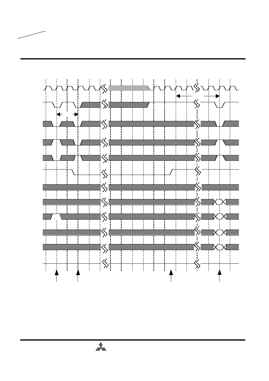
A WRITE command can be issued to any active bank.The start address is specified by A0-9,11(x4),
A0-9 (x8), A0-8 (x16). 1st input data is set at the same cycle as the WRITE. The consecutive data length
to be written is defined by the Burst Length. The address sequence of burst data is defined by the Burst
Type. Minimum delay time of a WRITE command after an ACT command to the same bank is tRCD.
From the last input data to the PRE command, the write recovery time (tWR) is required. When A10 is
high at a WRITE command, auto-precharge(WRITEA) is performed. Any command (READ, WRITE,
PRE, ACT, TBST) to the same bank is inhibited till the internal precharge is complete. The internal
precharge starts at tWR after the last input data cycle. The next ACT command can be issued after (BL
+ tWR ≠1 +tRP) from the previous WRITEA. In any case, tRCD + BL + tWR ≠1 > tRASmin must be
met.
WRITE
A0-9,11-12
CLK
Command
tRCD
ACT
Write
ACT
PRE
Xa
Ya
Xa
Xa
0
Xa
00
00
00
A10
BA0-1
DQ
tRP
0
Da2
Da3
Da0
Da1
BL
CLK
Command
tRCD
ACT
Write
ACT
Xa
Ya
Xa
Xa
1
Xa
00
00
00
A0-9,11-12
A10
BA0-1
DQ
Da2
Da3
Da0
Da1
BL
Internal precharge starts
Write with Auto-Precharge (BL=4)
Write(BL=4)
tWR
tWR
tRP
M2V56S20/ 30/ 40 TP ≠5,-5L, -6,-6L, -7,-7L
SDRAM (Rev.1.5E)
Single Data Rate
Oct.2001
256M Synchronous DRAM
MITSUBISHI LSIs
Preliminary
MITSUBISHI ELECTRIC
18
CLK
Command
READ
A0-9,11-12
A10
BA0-1
DQ
READ
Qa0
Qa1
Qa2
Qb0
Qc0
Qc1
Qc2
Qc3
Read interrupted by Read(CL=2, BL=4)
READ
Yb
0
Yc
0
00
0
Ya
0
00
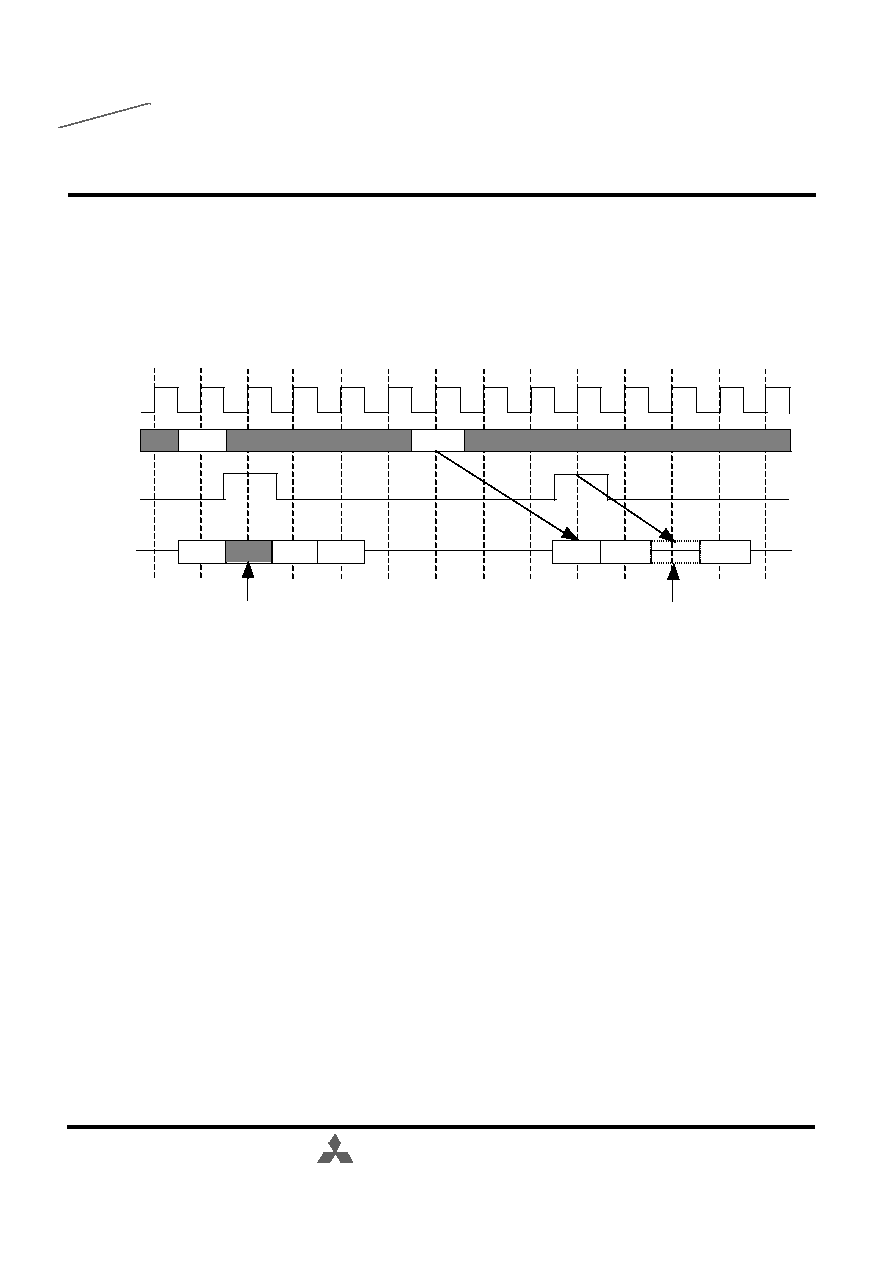
BURST INTERRUPUTION
[Read Interrupted by Read ]
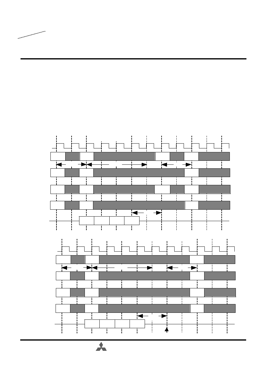
Burst read operation can be interrupted by new read of any active bank. Random column access is
allowed. READ to READ interval is minimum 1 CLK.
[Read Interrupted by Write ]
Burst read operation can be interrupted by write of any active bank. Random column access is allowed.
In this case, the DQ should be controlled adequately by using the DQM to prevent the bus contention.
The output is disabled automatically 2 cycle after WRITE assertion.
A0-9,11-12
CLK
Command
ACT
READ
Xa
Ya
Xa
0
00
00
A10
BA0-1
DQM
Da2
Da3
Da0
Da1
Write
Ya
0
00
DQ
Da0
Read interrupted by Write(CL=2, BL=4)
Output disable by DQM by WRITE

M2V56S20/ 30/ 40 TP ≠5,-5L, -6,-6L, -7,-7L
SDRAM (Rev.1.5E)
Single Data Rate
Oct.2001
256M Synchronous DRAM
MITSUBISHI LSIs
Preliminary
MITSUBISHI ELECTRIC
19
[ Read Interrupted by Precharge ]
A burst read operation can be interruted by a precharge of the same bank. READ to PRE interval is
minimum 1CLK.
A PRE command to output disable latency is equivalent to the /CAS Latency.
Read interrupted by Precharge (BL=4)
READ
PRE
READ
PRE
READ
PRE
Q0
Q1
Q2
Q0
Q1
Q0
CLK
Command
Command
Command
DQ
DQ
DQ
READ
PRE
READ
PRE
READ
PRE
Q0
Q1
Q2
Q0
Q1
Q0
Command
Command
Command
DQ
DQ
DQ
CL=2
CL=3
M2V56S20/ 30/ 40 TP ≠5,-5L, -6,-6L, -7,-7L
SDRAM (Rev.1.5E)
Single Data Rate
Oct.2001
256M Synchronous DRAM
MITSUBISHI LSIs
Preliminary
MITSUBISHI ELECTRIC
20
Read interrupted by Terminate (BL=4)
READ
TBST
READ
TBST
READ TBST
Q0
Q1
Q2
Q0
Q1
Q0
CLK
Command
Command
Command
DQ
DQ
DQ
READ
TBST
READ
TBST
READ TBST
Q0
Q1
Q2
Q0
Q1
Q0
Command
Command
Command
DQ
DQ
DQ
CL=2
CL=3
[ Read Interrupted by Burst Terminate]
Similarly to the precharge, a burst terminate command can interrupt the burst read operation and
disable the data output. The terminated bank remains active. READ to TBST interval is minimum 1
CLK. A TBST command to output disable latency is equivalent to the /CAS Latency.
M2V56S20/ 30/ 40 TP ≠5,-5L, -6,-6L, -7,-7L
SDRAM (Rev.1.5E)
Single Data Rate
Oct.2001
256M Synchronous DRAM
MITSUBISHI LSIs
Preliminary
MITSUBISHI ELECTRIC
21
CLK
Command
Write
A0-9,11-12
A10
BA0-1
DQ
Write
Da0
Da1
Da2
Db0
Dc0
Dc1
Dc2
Dc3
Write
Yb
0
Yc
0
00
10
Ya
0
00
[ Write Interrupted by Write ]
Burst write operation can be interruputed by new write of any active bank. Random column access is
allowed. WRITE to WRITE interval is minimum 1 CLK.
Write interrupted by Write(BL=4)
[ Write Interrupted by Read ]
Burst write operation can be interrupted by read of any active bank. Random column access is allowed.
WRITE to READ interval is minimum 1 CLK. The input data on DQ at the interrupting READ cycle is
"Don't Care".
Command
A0-9,11-12
CLK
ACT
A10
BA0-1
DQ
Da0
Da1
Qb0
Qb1
Qb2
Qb3
READ
Xa
Ya
Yb
Xa
0
00
00
00
don't care
Write
0
Write interrupted by Read(CL=2, BL=4)

M2V56S20/ 30/ 40 TP ≠5,-5L, -6,-6L, -7,-7L
SDRAM (Rev.1.5E)
Single Data Rate
Oct.2001
256M Synchronous DRAM
MITSUBISHI LSIs
Preliminary
MITSUBISHI ELECTRIC
22
[ Write Interrupted by Precharge ]
Burst write operation can be interruputed by precharge of the same bank. Write recovery time (tWR) is
required from the last data to PRE command. During write recovery, data inputs must be masked by DQM.
CLK
Command
ACT
A0-9,11-12
A10
BA0-1
DQ
Write
Da0
Da1
PRE
Ya
0
Xa
0
00
Xa
0
00
ACT
0
00
00
DQM
Write interrupted by Precharge (BL=4)
[ Write Interrupted by Burst Terminate ]
Burst terminate command can terminate burst write operation. In this case, the write recovery time is
not required and the bank remains active. WRITE to TBST interval is minimum 1 CLK.
CLK
Command
ACT
A10
BA0-1
DQ
Write
Db0
Db1
Ya
0
Yb
0
00
Xa
0
00
Write
00
Write interrupted by Terminate (BL=4)
A0-9,11-12
tRP
tWR
TBST
Da0
Da1
Db2
Db3
M2V56S20/ 30/ 40 TP ≠5,-5L, -6,-6L, -7,-7L
SDRAM (Rev.1.5E)
Single Data Rate
Oct.2001
256M Synchronous DRAM
MITSUBISHI LSIs
Preliminary
MITSUBISHI ELECTRIC
23
[ Write with Auto-Precharge Interrupted by Write / Read to another Bank ]
Burst write with auto-precharge can be interrupted by write or read to another bank. Next ACT
command can be issued after (BL+tWR-1+tRP) from the WRITEA. Auto-precharge interruption by a
command to the same bank is inhibited.
CLK
Command
Write
A0-9,11-12
A10
BA0-1
DQ
Da0
Da1
Db0
Db1
Db2
Db3
Write
Ya
1
00
ACT
Yb
Xa
0
Xa
10
00
auto-precharge
interrupted
activate
WRITEA interrupted by WRITE to another bank (BL=4)
CLK
Command
Write
A0-9,11-12
A10
BA0-1
DQ
Da0
Da1
Qb0
Qb1
Qb2
Qb3
Read
Ya
1
00
ACT
Yb
Xa
0
Xa
10
00
tWR
auto-precharge
interrupted
activate
WRITEA interrupted by READ to another bank (CL=2,BL=4)
BL
tRP
BL
tRP
tWR
M2V56S20/ 30/ 40 TP ≠5,-5L, -6,-6L, -7,-7L
SDRAM (Rev.1.5E)
Single Data Rate
Oct.2001
256M Synchronous DRAM
MITSUBISHI LSIs
Preliminary
MITSUBISHI ELECTRIC
24
Burst read with auto-precharge can be interrupted by read to another bank. Next ACT command can
be issued after (BL+tRP) from the READA. Auto-precharge interruption by a command to the same
bank is inhibited.
[ Read with Auto-Precharge Interrupted by Read to another Bank ]
CLK
Command
Read
A0-9,11-12
A10
BA0-1
DQ
Qa0
Qa1
Qb0
Qb1
Qb2
Qb3
Read
Ya
1
00
ACT
Yb
0
10
auto-precharge
interrupted
activate
READA interrupted by READ to another bank (CL=2,BL=4)
Xa
Xa
00
Full page burst length is available for only the sequential burst type. Full page burst read / write is
repeated untill a Precharge or a Burst Terminate command is issued. In case of the full page burst,
a read / write with auto-precharge command is illegal.
Full Page Burst
When single write mode is set, burst length for write is always one, independently of Burst Length
defined by (A2-0).
Single Write
BL
tRP

M2V56S20/ 30/ 40 TP ≠5,-5L, -6,-6L, -7,-7L
SDRAM (Rev.1.5E)
Single Data Rate
Oct.2001
256M Synchronous DRAM
MITSUBISHI LSIs
Preliminary
MITSUBISHI ELECTRIC
25
AUTO REFRESH
Single cycle of auto-refresh is initiated with a REFA (/CS= /RAS= /CAS=L, / WE= /CKE=H)
command. The refresh address is generated internally. 8192 REFA cycles within 64ms refresh 256Mbit
memory cells. The auto-refresh is performed on 4 banks concurrently. Before performing an auto-
refresh, all banks must be in idle state. Auto-refresh to auto-refresh interval is minimum tRFC. Any
command must not be issued before tRFC from the REFA command.
Auto-Refresh
CLK
/CS
/RAS
/CAS
/WE
CKE
minimum tRFC
Auto-Refresh on All Banks
Auto Refresh on All Banks
A0-12
BA0-1
NOP or DESELECT

M2V56S20/ 30/ 40 TP ≠5,-5L, -6,-6L, -7,-7L
SDRAM (Rev.1.5E)
Single Data Rate
Oct.2001
256M Synchronous DRAM
MITSUBISHI LSIs
Preliminary
MITSUBISHI ELECTRIC
26
SELF REFRESH
Self-refresh mode is entered by issuing a REFS command (/CS= /RAS= /CAS=L, /WE=H, CKE=L).
Once the self-refresh is initiated, it is maintained as long as CKE is kept low. During the self-refresh mode,
CKE is asynchronous and the only enabled input. All other inputs including CLK are disabled and
ignored, so that power consumption due to synchronous inputs is saved. To exit the self-refresh,
supplying stable CLK inputs, asserting DESEL or NOP command and then asserting CKE=H. After
tRFC from the 1st CLK edge following CKE=H, all banks are in idle state and a new command can be
issued, but DESEL or NOP commands must be asserted till then.
new command
Self-Refresh
CLK
/CS
/RAS
/CAS
/WE
CKE
NOP
Self Refresh Entry
Self Refresh Exit
Stable CLK
A0-12
BA0-1
X
00
minimum tRFC
for recovery
M2V56S20/ 30/ 40 TP ≠5,-5L, -6,-6L, -7,-7L
SDRAM (Rev.1.5E)
Single Data Rate
Oct.2001
256M Synchronous DRAM
MITSUBISHI LSIs
Preliminary
MITSUBISHI ELECTRIC
27
CKE controls the internal CLK at the following cycle. Figure below shows how CKE works. By
negating CKE, the next internal CLK is suspended. The purpose of CLK suspend is power down, output
suspend or input suspend. CKE is a synchronous input except during the self-refresh mode. CLK
suspend can be performed either when the banks are active or idle. A command at the suspend cycle is
Ignored.
CLK SUSPEND and POWER DOWN
tIH
tIS
tIH
tIS
ext.CLK
CKE
int. CLK
CLK
Command
CKE
PRE NOP
NOP
NOP
CKE
ACT NOP
NOP
NOP
Command
CLK
Command
DQ
Write
Read
CKE
D0
D1
D2
D3
Q0
Q1
Q2
Q3
Active Power Down
DQ Suspend by CKE
Power Down by CKE
Standby Power Down
M2V56S20/ 30/ 40 TP ≠5,-5L, -6,-6L, -7,-7L
SDRAM (Rev.1.5E)
Single Data Rate
Oct.2001
256M Synchronous DRAM
MITSUBISHI LSIs
Preliminary
MITSUBISHI ELECTRIC
28
DQMU/L is a dual functional signal defined as the data mask for writes and the output disable for
reads. During writes, DQMU/L masks input data word by word. DQMU/L to Data In latency is 0.
During reads, DQMU/L forces output to Hi-Z word by word. DQMU/L to output Hi-Z latency is 2.
DQM CONTROL
DQM Function
CLK
Command
DQ
DQMU/L
Write
Read
Q0
Q1
Q3
D0
D2
D3
masked by DQMU/L=H
disabled by DQMU/L=H
M2V56S20/ 30/ 40 TP ≠5,-5L, -6,-6L, -7,-7L
SDRAM (Rev.1.5E)
Single Data Rate
Oct.2001
256M Synchronous DRAM
MITSUBISHI LSIs
Preliminary
MITSUBISHI ELECTRIC
29
Symbol
Parameter
Conditions
Ratings
Unit
Vdd
Supply Voltage
with respect to Vss
-0.5 ~ 4.6
V
VddQ
Supply Voltage for Output
with respect to VssQ
-0.5 ~ 4.6
V
VI
Input Voltage
with respect to Vss
-0.5 ~ Vdd+0.5
V
VO
Output Voltage
with respect to VssQ
-0.5 ~ Vdd+0.5
V
IO
Output Current
50
mA
Pd
Power Dissipation
Ta=25∞C
1000
mW
Topr
Operating Temprature
0 ~ 70
∞C
Tstg
Storage Tempreture
-65 ~ 150
∞C
ABSOLUTE MAXIMUM RATINGS
RECOMMENDED OPERATING CONDITIONS
(Ta=0 ~ 70 ∞C, unless otherwise noted)
Min.
Typ.
Max.
Vdd
Supply Voltage
3.0
3.3
3.6
V
Vss
Supply Voltage
0
0
0
V
VddQ
Supply Voltage for Output
3.0
3.3
3.6
V
VssQ
Supply Voltage for Output
0
0
0
V
VIH
High-Level Input Voltage all inputs
2.0
Vdd+0.3
V
VIL
Low-Level Input Voltage all inputs
-0.3
0.8
V
Parameter
Symbol
Unit
Limits
CAPACITANCE
(Ta=0 ~ 70 ∞C, Vdd= VddQ= 3.3 ± 0.3V, Vss=VssQ=0V, unless otherwise noted)
Min.
Max.
CI(A)
Input Capacitance,address pin
2.5
3.8
pF
CI(C)
Input Capacitance,control pin
VI=1.4V
2.5
3.8
pF
CI(K)
Input Capacitance,CLK pin
f=1MHz
2.5
3.5
pF
CI/O
Input Capacitance,I/O pin
VI=25mVrms
4
6.5
pF
Unit
Symbol
Parameter
Test Condition
Limits
M2V56S20/ 30/ 40 TP ≠5,-5L, -6,-6L, -7,-7L
SDRAM (Rev.1.5E)
Single Data Rate
Oct.2001
256M Synchronous DRAM
MITSUBISHI LSIs
Preliminary
MITSUBISHI ELECTRIC
30
AVERAGE SUPPLY CURRENT from Vdd
(Ta=0 ~ 70∞C, Vdd= VddQ= 3.3 ± 0.3V, Vss= VssQ= 0V, Output Open, unless otherwise noted)
Notes
1.
addresses are changed 3 times during tRC, only 1 bank is active & all other banks are idle
2.
all banks are idle
3.
input signals are changed one time during 3xtCLK
4.
input signals are stable
5.
all banks are active
6.
Low Power Version (-5L/-6L/-7L)
Min.
Max.
VOH(DC)
High-Level Output Voltage(DC)
IOH=-2mA
2.4
V
VOL(DC)
Low-Level Output Voltage(DC)
IOL=2mA
0.4
V
IOZ
Off-state Output Current
Q floating Vo=0 ~ VddQ
-10
10
I
I
Input Current
VIH=0 ~ VddQ+0.3V, other input pins=0V
-10
10
Unit
Symbol
Parameter
Test Conditions
Limits
AC OPERATING CONDITIONS AND CHARACTERISTICS
(Ta=0 ~ 70∞C, Vdd= VddQ= 3.3 ± 0.3V, Vss= VssQ= 0V, unless otherwise noted)
µA
µA
organi
zation
-5
-6
-7
◊4
110
90
80
Operating Current
◊8
110
90
80
(1bank)
◊16
120
100
90
Icc2P
Idle Stanby Current
tCLK=min, CKE<VILmax
2
1.5
1
mA
Icc2PS in Power Down Mode CLK=L, CKE<VILmax
1
1
1
mA
Idle Stanby Current
tCLK=min, CKE>VIHmin,
in Normal Mode
/CS>VIHmin
Icc2NS
CLK=L, CKE>VIHmin
6
6
6
mA
2,4
Icc3P
Active Standy
tCLK=min, CKE<VILmax
6
5
4
mA
Current
in Power Down Mode
Active Standy
tCLK=min, CKE>VIHmin
Current
/CS>VIHmin
Icc3NS in Normal Mode
CLK=L, CKE>VIHmin
15
15
15
mA
4,5
◊4
140
110
90
Burst Operating
tCLK=min,BL=4, gapless
◊8
140
110
90
Current
data
◊16
150
120
100
Icc5
Auto-Refresh Current
tCLK=min,tRFC=min
220
180
170
mA
3
3
3
mA
2
2
2
mA
6
-5L/-6L/-7L
Icc6
Self-Refresh Current
2
Icc2N
30
25
20
mA
2,3
CKE<0.2v -5/-6/-7
Unit
Note
Icc1
tCLK=min, tRC=min, BL=1
mA
1
Symbol
Parameter
Test Conditions
Limits(max)
Icc3PS
CLK=L, CKE<VILmax
4
4
4
mA
5
25
mA
3,5
Icc4
Icc3N
35
30
mA
5
M2V56S20/ 30/ 40 TP ≠5,-5L, -6,-6L, -7,-7L
SDRAM (Rev.1.5E)
Single Data Rate
Oct.2001
256M Synchronous DRAM
MITSUBISHI LSIs
Preliminary
MITSUBISHI ELECTRIC
AC TIMING REQUIREMENTS
(Ta=0 ~ 70∞C, Vdd= VddQ= 3.3 ± 0.3V, Vss= VssQ= 0V, unless otherwise noted)
Input Pulse Levels: 0.8V to 2.0V
Input Timing Measurement Level: 1.4V
1.4V
1.4V
CLK
Signal
AC timing is referenced to the
input signal crossing through
1.4V.
31
Min.
Max.
Min.
Max.
Min.
Max.
CL=2
7.5
10
10
ns
CL=3
6
7.5
10
ns
tCH
CLK High pulse width
2.5
2.5
3
ns
tCL
CLK Low pulse width
2.5
2.5
3
ns
tT
Transition time of CLK
1
10
1
10
1
10
ns
tIS
Input Setup time (all inputs)
1.5
1.5
2
ns
tIH
Input Hold time (all inputs)
0.8
0.8
1
ns
tRC
Row Cycle time
60
67.5
70
ns
tRFC
Refresh Cycle time
66
75
80
ns
tRCD
Row to Column Delay
15
20
20
ns
tRP
Row Precharge time
15
20
20
ns
tWR
Write Recovery time
12
15
20
ns
tRRD
ACT to ACT Delay time
12
15
20
ns
Mode Register Set Cycle
time
tREF
Average Refresh Interval
7.8
7.8
7.8
Unit Note
Limits
Symbol
Parameter
-5
-6
-7
tCLK
tRAS
45
120000
tRSC
Row Active time
42
120000
10
10
10
50
120000 ns
ns
CLK cycle time
µs
M2V56S20/ 30/ 40 TP ≠5,-5L, -6,-6L, -7,-7L
SDRAM (Rev.1.5E)
Single Data Rate
Oct.2001
256M Synchronous DRAM
MITSUBISHI LSIs
Preliminary
MITSUBISHI ELECTRIC
32
SWITCHING CHARACTERISTICS
(Ta=0 ~ 70∞C, Vdd= VddQ= 3.3 ± 0.3V, Vss= VssQ= 0V, unless otherwise noted)
Min.
Max.
Min.
Max.
Min.
Max.
CL=2
5.4
6
6
ns
CL=3
5.4
5.4
6
ns
CL=2
3
3
3
ns
CL=3
3
3
3
ns
Delay Time, Output Low
impedance from CLK
Delay Time, Output High
impedance from CLK
Limits
Symbol
Parameter
-5
-6
-7
3
6
ns
CL=2
5.4
3
6
tAC
tOH
tOLZ
tOHZ
3
3
5.4
3
5.4
0
ns
CL=3
Access Time from CLK
Output Hold Time from CLK
Unit
3
6
ns
0
0
Note. If tr (CLK rising time) is > 1ns, (tr/2 ≠ 0.5ns) should be added to the parameters.
Output Load Condition
Vout
50pF
tOHZ
tOH
tOLZ
tAC
CLK
DQ
1.4V
1.4V
M2V56S20/ 30/ 40 TP ≠5,-5L, -6,-6L, -7,-7L
SDRAM (Rev.1.5E)
Single Data Rate
Oct.2001
256M Synchronous DRAM
MITSUBISHI LSIs
Preliminary
MITSUBISHI ELECTRIC
33
Burst Write (Single Bank) [BL=4]
tRC
0
1
tRAS
2
3
4
5
6
7
8
9
10
11
12
13
14
15
16
tRP
tRCD
tRCD
tWR
tWR
X
Y
X
Y
X
X
X
X
0
0
0
0
0
0
D0
D0
D0
D0
D0
D0
D0
D0
ACT#0
PRE#0
WRITE#0
ACT#0
WRITE#0
PRE#0
BA0,1
CLK
/CS
/RAS
/CAS
/WE
CKE
DQM
A0-9,11
A10
A12
DQ
Italic paramater shows minimum case
M2V56S20/ 30/ 40 TP ≠5,-5L, -6,-6L, -7,-7L
SDRAM (Rev.1.5E)
Single Data Rate
Oct.2001
256M Synchronous DRAM
MITSUBISHI LSIs
Preliminary
MITSUBISHI ELECTRIC
34
Italic paramater shows minimum case
Burst Write (Multi Bank) [BL=4]
tRC
0
1
tRAS
2
3
4
5
6
7
8
9
10
11
12
13
14
15
16
tRP
tRCD
tRCD
tWR
X
X
X
X
0
0
0
0
D0
D0
D0
D0
D0
D0
D0
D0
ACT#0
PRE#0
WRITE#0
ACT#0
WRITE#0
PRE#0
tRRD
tWR
tRCD
DQ
X
Y
X
Y
X
Y
X
CLK
/CS
/RAS
/CAS
/WE
DQM
A0-9,11
CKE
BA0,1
A10
A12
X
X
X
X
0
1
1
0
1
D1
D1
D1
D1
WRITEA#1
(Auto-Precharge)
ACT#1
ACT#1
tRC
M2V56S20/ 30/ 40 TP ≠5,-5L, -6,-6L, -7,-7L
SDRAM (Rev.1.5E)
Single Data Rate
Oct.2001
256M Synchronous DRAM
MITSUBISHI LSIs
Preliminary
MITSUBISHI ELECTRIC
35
Italic paramater shows minimum case
Burst Read (Single Bank) [CL=2, BL=4]
tRC
0
1
tRAS
2
3
4
5
6
7
8
9
10
11
12
13
14
15
16
tRP
tRCD
tRCD
X
Y
X
Y
X
X
X
X
0
0
0
0
0
0
Q0
Q0
Q0
Q0
Q0
Q0
Q0
Q0
ACT#0
PRE#0
READ#0
ACT#0
READ#0
PRE#0
tRAS
BA0,1
CLK
/CS
/RAS
/CAS
/WE
CKE
DQM
A0-9,11
A10
A12
DQ
M2V56S20/ 30/ 40 TP ≠5,-5L, -6,-6L, -7,-7L
SDRAM (Rev.1.5E)
Single Data Rate
Oct.2001
256M Synchronous DRAM
MITSUBISHI LSIs
Preliminary
MITSUBISHI ELECTRIC
36
Italic paramater shows minimum case
Burst Read (Multi Bank) [CL=2, BL=4]
tRC
0
1
tRAS
2
3
4
5
6
7
8
9
10
11
12
13
14
15
16
tRCD
tRCD
X
X
X
X
0
0
0
0
Q0
Q0
Q0
Q0
Q0
Q0
Q0
Q0
ACT#0 READA#0
ACT#0
READ#0
PRE#0
tRRD
tRCD
X
Y
X
Y
X
Y
X
X
X
X
X
0
1
1
1
Q1
Q1
Q1
Q1
ACT#1
tRC
READA#1
ACT#1
DQ
CLK
/CS
/RAS
/CAS
/WE
DQM
A0-9,11
CKE
BA0,1
A10
A12
M2V56S20/ 30/ 40 TP ≠5,-5L, -6,-6L, -7,-7L
SDRAM (Rev.1.5E)
Single Data Rate
Oct.2001
256M Synchronous DRAM
MITSUBISHI LSIs
Preliminary
MITSUBISHI ELECTRIC
37
Italic paramater shows minimum case
Write Interrupted by Write [BL=4]
0
1
2
3
4
5
6
7
8
9
10
11
12
13
14
15
16
tRCD
tWR
X
X
0
0
D0
D0
D0
D0
D0
D0
D0
D0
ACT#0 WRITE#0
WRITE#0
interrupt
other
bank
PRE#0
tRRD
X
Y
Y
X
Y
X
X
X
X
0
1
1
0
D0
D1
D1
D1
WRITEA#1
interrupt
other
bank
ACT#1
DQ
CLK
/CS
/RAS
/CAS
/WE
DQM
A0-9,11
CKE
BA0,1
A10
A12
Y
X
0
1
WRITE#0
interrupt
same
bank
ACT#1
M2V56S20/ 30/ 40 TP ≠5,-5L, -6,-6L, -7,-7L
SDRAM (Rev.1.5E)
Single Data Rate
Oct.2001
256M Synchronous DRAM
MITSUBISHI LSIs
Preliminary
MITSUBISHI ELECTRIC
38
Italic paramater shows minimum case
Read Interrupted by Read [CL=2, BL=4]
0
1
2
3
4
5
6
7
8
9
10
11
12
13
14
15
16
tRCD
X
X
0
0
Q0
Q0
Q0
Q1
Q0
Q0
Q0
Q0
ACT#0 READ#0
READ#0
interrupt
other
bank
tRRD
X
Y
Y
X
Y
X
X
X
X
0
1
1
Q1
Q1
Q1
Q1
READA#1
Interrupt
same bank
ACT#1
DQ
CLK
/CS
/RAS
/CAS
/WE
DQM
A0-9,11
CKE
BA0,1
A10
A12
Y
READ#1
interrupt
other
bank
ACT#1
X
1
1
tRCD
M2V56S20/ 30/ 40 TP ≠5,-5L, -6,-6L, -7,-7L
SDRAM (Rev.1.5E)
Single Data Rate
Oct.2001
256M Synchronous DRAM
MITSUBISHI LSIs
Preliminary
MITSUBISHI ELECTRIC
39
Italic paramater shows minimum case
Write Interrupted by Read, Read Interrupted by Write [CL=2, BL=4]
0
1
2
3
4
5
6
7
8
9
10
11
12
13
14
15
16
tRCD
tWR
X
X
0
D0
D0
D1
D1
D1
D1
ACT#0
WRITE#0
WRITE#1
PRE#1
tRRD
X
Y
X
Y
X
0
1
1
Q1
Q1
Y
1
READ#1
ACT#1
tRCD
X
1
DQ
CLK
/CS
/RAS
/CAS
/WE
DQM
A0-9,11
CKE
BA0,1
A10
A12

M2V56S20/ 30/ 40 TP ≠5,-5L, -6,-6L, -7,-7L
SDRAM (Rev.1.5E)
Single Data Rate
Oct.2001
256M Synchronous DRAM
MITSUBISHI LSIs
Preliminary
MITSUBISHI ELECTRIC
40
Italic paramater shows minimum case
Write / Read Terminated by Precharge [CL=2, BL=4]
tRC
0
1
tRAS
2
3
4
5
6
7
8
9
10
11
12
13
14
15
16
tRCD
tRP
X
X
X
0
0
0
0
D0
D0
Q0
Q0
ACT#0 WRITE#0
ACT#0
READ#0 PRE#0
Terminate
tRCD
X
Y
X
Y
X
X
X
0
0
DQ
CLK
/CS
/RAS
/CAS
/WE
DQM
A0-9,11
CKE
BA0,1
A10
A12
tRP
tWR
X
0
ACT#0
PRE#0
Terminate

M2V56S20/ 30/ 40 TP ≠5,-5L, -6,-6L, -7,-7L
SDRAM (Rev.1.5E)
Single Data Rate
Oct.2001
256M Synchronous DRAM
MITSUBISHI LSIs
Preliminary
MITSUBISHI ELECTRIC
41
Italic paramater shows minimum case
Write / Read Terminated by Burst Terminate [CL=2, BL=4]
0
1
2
3
4
5
6
7
8
9
10
11
12
13
14
15
16
tRCD
tWR
X
X
0
0
D0
D0
D0
D0
D0
D0
ACT#0 WRITE#0
WRITE#0
PRE#0
X
Y
Y
0
0
Q0
Q0
TBST
DQ
CLK
/CS
/RAS
/CAS
/WE
DQM
A0-9,11
CKE
BA0,1
A10
A12
Y
0
READ#0
TBST

M2V56S20/ 30/ 40 TP ≠5,-5L, -6,-6L, -7,-7L
SDRAM (Rev.1.5E)
Single Data Rate
Oct.2001
256M Synchronous DRAM
MITSUBISHI LSIs
Preliminary
MITSUBISHI ELECTRIC
42
Italic paramater shows minimum case
Single Write Burst Read [CL=2, BL=4]
0
1
2
3
4
5
6
7
8
9
10
11
12
13
14
15
16
tRCD
X
Y
Y
X
X
0
0
0
D0
Q0
Q0
Q0
Q0
ACT#0 WRITE#0 READ#0
BA0,1
CLK
/CS
/RAS
/CAS
/WE
CKE
DQM
A0-9,11
A10
A12
DQ

M2V56S20/ 30/ 40 TP ≠5,-5L, -6,-6L, -7,-7L
SDRAM (Rev.1.5E)
Single Data Rate
Oct.2001
256M Synchronous DRAM
MITSUBISHI LSIs
Preliminary
MITSUBISHI ELECTRIC
43
Italic paramater shows minimum case
Power-Up Sequence and Intialize
tRP
X
MA
PRE ALL
ACT#0
MRS
X
0
X
0
0
0
REFA
Power On
BA0,1
CLK
/CS
/RAS
/CAS
/WE
CKE
DQM
A0-9,11
A10
A12
DQ
tRFC
tRSC
tRFC
NOP
REFA
REFA
Minimum 2 REFA cycles
100µs
M2V56S20/ 30/ 40 TP ≠5,-5L, -6,-6L, -7,-7L
SDRAM (Rev.1.5E)
Single Data Rate
Oct.2001
256M Synchronous DRAM
MITSUBISHI LSIs
Preliminary
MITSUBISHI ELECTRIC
44
Italic paramater shows minimum case
Auto Refresh
tRFC
0
1
2
3
4
5
6
7
8
9
10
11
12
13
14
15
16
tRP
tRCD
X
Y
X
D0
D0
D0
D0
PRE ALL
REFA
ACT#0
WRITE#0
X
0
0
BA0,1
CLK
/CS
/RAS
/CAS
/WE
CKE
DQM
A0-9,11
A10
A12
DQ
All banks must be idle before REFA is issued.
M2V56S20/ 30/ 40 TP ≠5,-5L, -6,-6L, -7,-7L
SDRAM (Rev.1.5E)
Single Data Rate
Oct.2001
256M Synchronous DRAM
MITSUBISHI LSIs
Preliminary
MITSUBISHI ELECTRIC
45
Italic paramater shows minimum case
Self Refresh
0
1
2
3
4
6
7
8
9
10
11
12
13
15
16
tRP
X
PRE ALL Self Refresh Entry
Self Refresh Exit
0
All banks must be idle before REFS is issued.
X
X
BA0,1
CLK
/CS
/RAS
/CAS
/WE
CKE
DQM
A0-9,11
A10
A12
DQ
ACT#0
5
14
tRFC
M2V56S20/ 30/ 40 TP ≠5,-5L, -6,-6L, -7,-7L
SDRAM (Rev.1.5E)
Single Data Rate
Oct.2001
256M Synchronous DRAM
MITSUBISHI LSIs
Preliminary
MITSUBISHI ELECTRIC
46
Italic paramater shows minimum case
CLK Suspension [CL=2, BL=4]
0
1
2
3
4
5
6
7
8
9
10
11
12
13
14
15
16
tRCD
X
Y
Y
X
X
0
0
0
Q0
Q0
Q0
ACT#0 WRITE#0
READ#0
BA0,1
CLK
/CS
/RAS
/CAS
/WE
CKE
DQM
A0-9,11
A10
A12
DQ
D0
D0
D0
D0
Q0
internal
CLK
suspended
internal
CLK
suspended

M2V56S20/ 30/ 40 TP ≠5,-5L, -6,-6L, -7,-7L
SDRAM (Rev.1.5E)
Single Data Rate
Oct.2001
256M Synchronous DRAM
MITSUBISHI LSIs
Preliminary
MITSUBISHI ELECTRIC
47
Italic paramater shows minimum case
Power Down
0
1
2
3
4
5
6
7
8
9
10
11
12
13
14
15
16
Standy Power Down
ACT#0
PRE ALL
Active Power Down
X
X
X
0
BA0,1
CLK
/CS
/RAS
/CAS
/WE
CKE
DQM
A0-9,11
A10
A12
DQ
M2V56S20/ 30/ 40 TP ≠5,-5L, -6,-6L, -7,-7L
SDRAM (Rev.1.5E)
Single Data Rate
Oct.2001
256M Synchronous DRAM
MITSUBISHI LSIs
Preliminary
MITSUBISHI ELECTRIC
48
1. These materials are intended as a reference to assist our customers in the selection of the Mitsubishi
semiconductor product best suited to the customer's application; they do not convey any license
under any intellectual property rights, or any other rights, belonging to Mitsubishi Electric Corporation or
a third party.
2. Mitsubishi Electric Corporation assumes no responsibility for any damage, or infringement of any
third-party's rights, originating in the use of any product data, diagrams, charts, programs, algorithms,
or circuit application examples contained in these materials.
3. All information contained in these materials, including product data, diagrams, charts, programs and
algorithms represents information on products at the time of publication of these materials, and are
subject to change by Mitsubishi Electric Corporation without notice due to product improvements or
other reasons. It is therefore recommended that customers contact Mitsubishi Electric Corporation or an
authorized Mitsubishi Semiconductor product distributor for the latest product information before
purchasing a product listed herein.
The information described here may contain technical inaccuracies or typographical errors. Mitsubishi
Electric Corporation assumes no responsibility for any damage, liability, or other loss rising from these
inaccuracies or errors. Please also pay attention to information published by Mitsubishi Electric
Corporation by various means, including the Mitsubishi Semiconductor home page
(http://www.mitsubishichips.com).
4. When using any or all of the information contained in these materials, including product data,
diagrams, charts, programs, and algorithms, please be sure to evaluate all information as a total
system before making a final decision on the applicability of the information and products. Mitsubishi
Electric Corporation assumes no responsibility for any damage, liability or other loss resulting from the
Information contained herein.
5. Mitsubishi Electric Corporation semiconductors are not designed or manufactured for use in a device
or system that is used under circumstances in which human life is potentially at stake. Please contact
Mitsubishi Electric Corporation or an authorized Mitsubishi semiconductor product distributor when
considering the use of a product contained herein for any specific purposes, such as apparatus or
systems for transportation, vehicular, medical, aerospace, nuclear, or undersea repeater use.
6. The prior written approval of Mitsubishi Electric Corporation is necessary to reprint or reproduce in
whole or in part these materials.
7. If these products or technologies are subject to the Japanese export control restrictions, they must
be exported under a license from the Japanese government and cannot be imported into a country other
than the approved destination. Any diversion or reexport contrary to the export control laws and
regulations of Japan and /or the country of destination is prohibited.
8. Please contact Mitsubishi Electric Corporation or an authorized Mitsubishi Semiconductor product
distributor for further details on these materials or the products contained therein.
Notes regarding these materials
Mitsubishi Electric Corporation puts the maximum effort into making semiconductor products better
and more reliable, but there is always the possibility that trouble may occur with them. Trouble with
semiconductors may lead to personal injury, fire or property damage. Remember to give due
consideration to safety when making your circuit designs, with appropriate measures such as (i)
placement of substitutive, auxiliary circuits, (ii) use of non-flammable material or (iii) prevention
against any malfunction or mishap.
Keep safety first in your circuit designs !
M2V56S20/ 30/ 40 TP ≠5,-5L, -6,-6L, -7,-7L
SDRAM (Rev.1.5E)
Single Data Rate
Oct.2001
256M Synchronous DRAM
MITSUBISHI LSIs
Preliminary
MITSUBISHI ELECTRIC
Rev.
Date
Description
1.0
July/ '99 1st edition
1.1
Feb. / '00 -Remove "Power-Down" from Function Truth Table for CKE Note2
-Modify Average Supply Current from Vdd
Icc2N,Icc3N Test Condition(/CS > VIHmin)
Icc3PS Limits (from 3mA to 4mA)
Icc5 Limits (from 160/150mA to 180/170mA)
Icc6 Test Condition (CKE<0.2V)
Icc6 Limits (from 2mA to 3mA)
-Change Switching Characteristics tAC of -8 for CL=2 from 6ns to 7ns
-Add Note to Switching Characteristics
-Change Output Load Condition to 50pF only
-Remove tCCD from AC Timing Requirements
1.2
Jan. / '01 -Add -5 spec. for M2V56S20TP only
1.3
Feb. / '01 -Add 166MHz of 3-3-3 for M2V56S20TP only
1.4
Mar. / '01 -Add -5 spec. for M2V56S20TP/30TP/40TP
1.45
May / '01 -Add Low Power Ver. -5L/-6L/-7L spec. for M2V56S20TP/30TP/40TP
1.5
Oct. / '01 -Change POWER ON SEQUENCE
(2. 200us=>100us
4. 8or more auto-refresh commands => 2 or more auto-refresh commands)
-Change AC Timing Requirements tRFC of -5 from 60ns to 66ns
-Change AC Timing Requirements tRSC of (-5/-6/-7)
from (12ns/15ns/20ns) to (10ns/10ns/10ns)
Revision History
49