Apr. '99
MITSUBISHI LSIs
MITSUBISHI ELECTRIC
SDRAM (Rev.1.2)
M2V64S20BTP-7,-7L,-8,-8L,-8A,-10,-10L (4-BANK x 4194304-WORD x 4-BIT)
M2V64S30BTP-7,-7L,-8,-8L,-8A,-10,-10L (4-BANK x 2097152-WORD x 8-BIT)
M2V64S40BTP-7,-7L,-8,-8L,-8A,-10,-10L (4-BANK x 1048576-WORD x 16-BIT)
64M bit Synchronous DRAM
1
DESCRIPTION
The M2V64S20BTP is organized as 4-bank x 4194304-word x 4-bit, M2V64S30BTP is
organized as 4-bank x 2097152-word x 8-bit, and M2V64S40BTP is organized as 4-bank x
1048576-word x 16-bit Synchronous DRAM with LVTTL interface. All inputs and outputs are
referenced to the rising edge of CLK. The M2V64S20BTP, M2V64S30BTP, M2V64S40BTP
achieve very high speed data rate up to 125MHz, and are suitable for main memory or
graphic memory in computer systems.
FEATURES
- Single 3.3v ± 0.3v power supply
- Fully synchronous operation referenced to clock rising edge
- 4 bank operation controlled by BA0, BA1 (Bank Address)
- /CAS latency- 2/3 (programmable)
- Burst length- 1/2/4/8/Full Page (programmable)
- Burst type- sequential / interleave (programmable)
- Column access - random
- Burst Write / Single Write (programmable)
- Auto refresh and Self refresh
- 4096 refresh cycles /64ms
- Column address A0-A9 (x4), A0-A8(x8), A0-A7(x16)
- LVTTL Interface
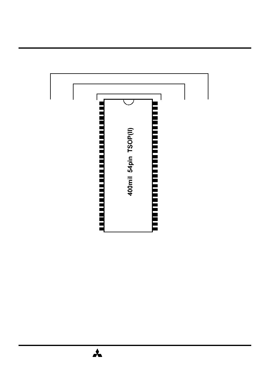
- 400-mil, 54-pin Thin Small Outline Package (TSOP II) with 0.8mm lead pitch
Max.
Frequency
CLK Access
Time
M2V64S20BTP
M2V64S30BTP
M2V64S40BTP
125MHz
6ns
- Clock frequency 125MHz /100MHz
100MHz(CL3)
6ns
-8A
100MHz(CL2)
6ns
- Auto precharge / All bank precharge controlled by A10
-7, -7L
-8, -8L
-10, -10L
100MHz
8ns
Apr. '99
MITSUBISHI LSIs
MITSUBISHI ELECTRIC
SDRAM (Rev.1.2)
M2V64S20BTP-7,-7L,-8,-8L,-8A,-10,-10L (4-BANK x 4194304-WORD x 4-BIT)
M2V64S30BTP-7,-7L,-8,-8L,-8A,-10,-10L (4-BANK x 2097152-WORD x 8-BIT)
M2V64S40BTP-7,-7L,-8,-8L,-8A,-10,-10L (4-BANK x 1048576-WORD x 16-BIT)
64M bit Synchronous DRAM
2
CLK
: Master Clock
CKE
: Clock Enable
/CS
: Chip Select
/RAS
: Row Address Strobe
/CAS
: Column Address Strobe
/WE
: Write Enable
DQ0-3(x4), DQ0-7(x8), DQ0-15(x16) : Data I/O
DQM (x4, x8) ,DQML/U (x16)
: Output Disable/ Write Mask
A0-11
: Address Input
BA0,1
: Bank Address
Vdd
: Power Supply
VddQ
: Power Supply for Output
Vss
: Ground
VssQ
: Ground for Output
PIN CONFIGURATION (TOP VIEW)
1
2
3
4
5
6
7
8
9
10
11
12
13
14
15
16
17
18
19
20
21
22
54
53
52
51
50
49
48
47
46
45
44
43
42
41
40
39
38
37
36
35
34
33
Vdd
DQ0
VddQ
DQ2
VssQ
DQ4
VddQ
DQ6
VssQ
Vdd
DQML
/WE
/CAS
/RAS
/CS
BA0(A13)
BA1(A12)
A10
Vss
DQ15
VssQ
DQ13
VddQ
DQ11
VssQ
DQ9
VddQ
Vss
NC
DQMU
CLK
CKE
NC
A11
A8
A7
23
32
24
31
25
30
26
29
27
28
A2
A3
Vdd
A0
A1
A6
A5
A4
Vss
A9
DQ1
DQ3
DQ5
DQ7
DQ8
DQ10
DQ12
DQ14
VddQ
DQ0
VssQ
VddQ
DQ1
VssQ
/CAS
/RAS
BA0(A13)
BA1(A12)
Vdd
NC
NC
NC
NC
Vdd
NC
/WE
/CS
A10
A2
A3
Vdd
A0
A1
NC
NC
Vss
VssQ
NC
DQ3
VddQ
NC
VssQ
NC
DQ2
VddQ
NC
Vss
NC
DQM
CLK
CKE
NC
A11
A8
A7
A6
A5
A4
Vss
A9
NC
NC
Vss
DQ7
VssQ
NC
DQ6
VddQ
NC
DQ5
VssQ
NC
DQ4
VddQ
NC
Vss
NC
DQM
CLK
CKE
NC
A11
A8
A7
A6
A5
A4
Vss
A9
Vdd
DQ0
VddQ
NC
DQ1
VssQ
NC
DQ2
VddQ
NC
DQ3
VssQ
NC
Vdd
NC
/WE
/CAS
/RAS
/CS
BA0(A13)
BA1(A12)
A10
A2
A3
Vdd
A0
A1
M2V64S40BTP
M2V64S30BTP
M2V64S20BTP
Apr. '99
MITSUBISHI LSIs
MITSUBISHI ELECTRIC
SDRAM (Rev.1.2)
M2V64S20BTP-7,-7L,-8,-8L,-8A,-10,-10L (4-BANK x 4194304-WORD x 4-BIT)
M2V64S30BTP-7,-7L,-8,-8L,-8A,-10,-10L (4-BANK x 2097152-WORD x 8-BIT)
M2V64S40BTP-7,-7L,-8,-8L,-8A,-10,-10L (4-BANK x 1048576-WORD x 16-BIT)
64M bit Synchronous DRAM
3
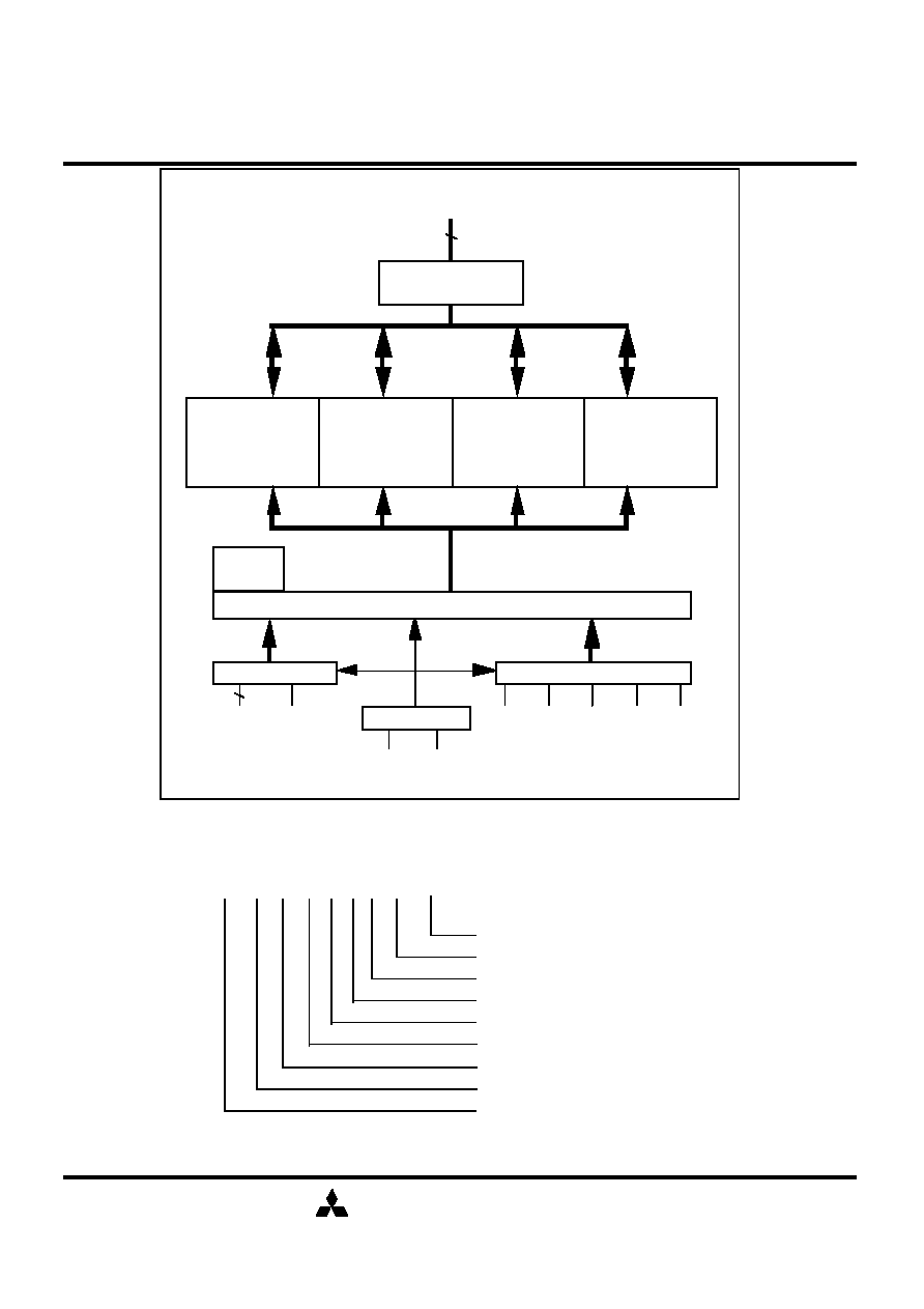
BLOCK DIAGRAM
Address Buffer
A0-11 BA0,1
Control Signal Buffer
/CS /RAS /CAS /WE DQM
CLK CKE
Clock Buffer
Memory Array
Bank #0
Control Circuitry
I/O Buffer
DQ0-3 (x4)
DQ0-7 (x8)
DQ0-15 (x16)
Mode
Register
Memory Array
Bank #1
Memory Array
Bank #2
Memory Array
Bank #3
Type Designation Code
M2 V 64 S 2 0 B TP - 7
Access Item
Package Type TP: TSOP(II)
Process Generation
Function 0: Random Column
Organization 2n 2: x4, 3: x8, 4: x16
Synchronous DRAM
Density 64:64M bits
Interface S: SSTL, V:LVTTL
Mitsubishi Semiconductor Memory
This rule is applied only to Synchronous DRAM families beyond 64M B-version.
Apr. '99
MITSUBISHI LSIs
MITSUBISHI ELECTRIC
SDRAM (Rev.1.2)
M2V64S20BTP-7,-7L,-8,-8L,-8A,-10,-10L (4-BANK x 4194304-WORD x 4-BIT)
M2V64S30BTP-7,-7L,-8,-8L,-8A,-10,-10L (4-BANK x 2097152-WORD x 8-BIT)
M2V64S40BTP-7,-7L,-8,-8L,-8A,-10,-10L (4-BANK x 1048576-WORD x 16-BIT)
64M bit Synchronous DRAM
4
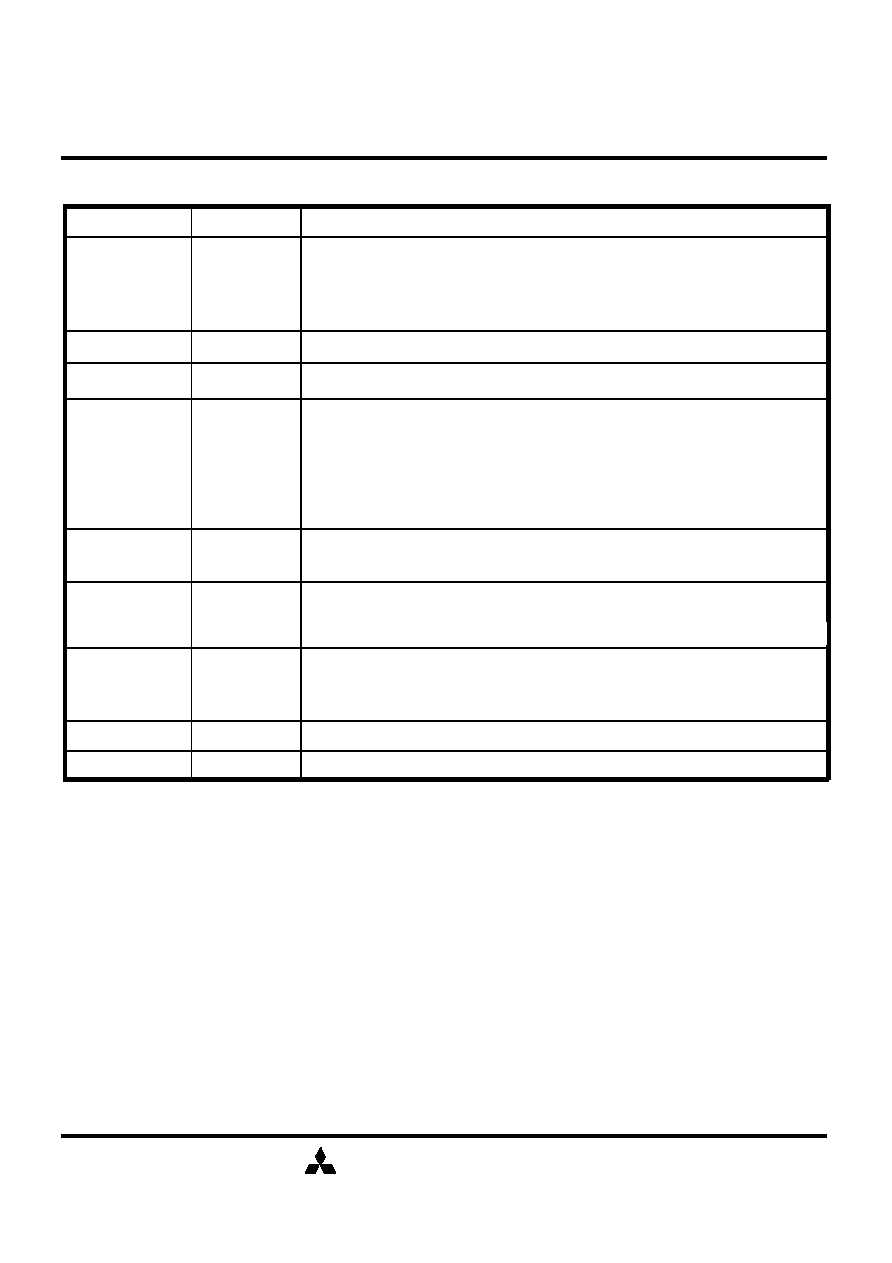
PIN FUNCTION
CLK
Input
Master Clock: All other inputs are referenced to the rising edge of CLK.
CKE
Input
Clock Enable: CKE controls internal clock. When CKE is low, internal clock
for the following cycle is ceased. CKE is also used to select auto / self
refresh. After self refresh mode is started, CKE becomes asynchronous
input. Self refresh is maintained as long as CKE is low.
/CS
Input
Chip Select: When /CS is high, any command means No Operation.
/RAS, /CAS, /WE
Input
Combination of /RAS, /CAS, /WE defines basic commands.
A0-11
Input
A0-11 specify the Row / Column Address in conjunction with BA0,1. The
Row Address is specified by A0-11. The Column Address is specified by
A0-A9(x4), A0-A8(x8), A0-7(x16) . A10 is also used to indicate precharge
option. When A10 is high at a read / write command, an auto precharge
is performed. When A10 is high at a precharge command, all banks are
precharged.
BA0,1
Input
Bank Address: BA0,1 specifies one of four banks to which a command is
applied. BA0,1 must be set with ACT, PRE, READ, WRITE commands.
DQ0-3(x4),
DQ0-7(x8),
DQ0-15(x16)
Input / Output
Data In and Data out are referenced to the rising edge of CLK.
DQM(x4,x8),
DQMU/L(x16)
Input
Din Mask / Output Disable: When DQMU/L is high in burst write, Din for the
current cycle is masked. When DQMU/L is high in burst read,
Dout is disabled at the next but one cycle.
Vdd, Vss
Power Supply
Power Supply for the memory array and peripheral circuitry.
VddQ, VssQ
Power Supply
VddQ and VssQ are supplied to the Output Buffers only.

Apr. '99
MITSUBISHI LSIs
MITSUBISHI ELECTRIC
SDRAM (Rev.1.2)
M2V64S20BTP-7,-7L,-8,-8L,-8A,-10,-10L (4-BANK x 4194304-WORD x 4-BIT)
M2V64S30BTP-7,-7L,-8,-8L,-8A,-10,-10L (4-BANK x 2097152-WORD x 8-BIT)
M2V64S40BTP-7,-7L,-8,-8L,-8A,-10,-10L (4-BANK x 1048576-WORD x 16-BIT)
64M bit Synchronous DRAM
5
BASIC FUNCTIONS
The M2V64S20(30,40)BTP provides basic functions, bank (row) activate, burst read / write,
bank (row) precharge, and auto / self refresh.
Each command is defined by control signals of /RAS, /CAS and /WE at CLK rising edge. In
addition to 3 signals, /CS ,CKE and A10 are used as chip select, refresh option, and
precharge option, respectively. To know the detailed definition of commands, please see the
command truth table.
/CS
Chip Select : L=select, H=deselect
/RAS
Command
/CAS
Command
/WE
Command
CKE
Refresh Option @refresh command
A10
Precharge Option @precharge or read/write command
CLK
define basic commands
Activate (ACT) [/RAS =L, /CAS =/WE =H]
ACT command activates a row in an idle bank indicated by BA.
Read (READ) [/RAS =H, /CAS =L, /WE =H]
READ command starts burst read from the active bank indicated by BA. First output data
appears after /CAS latency. When A10 =H at this command, the bank is deactivated after the
burst read (auto-precharge,
READA).
Write (WRITE) [/RAS =H, /CAS =/WE =L]
WRITE command starts burst write to the active bank indicated by BA. Total data length to be
written is set by burst length. When A10 =H at this command, the bank is deactivated after the
burst write (auto-precharge,
WRITEA).
Precharge (PRE) [/RAS =L, /CAS =H, /WE =L]
PRE command deactivates the active bank indicated by BA. This command also terminates
burst read /write operation. When A10 =H at this command, both banks are deactivated
(precharge all,
PREA).
Auto-Refresh (REFA) [/RAS =/CAS =L, /WE =CKE =H]
REFA command starts auto-refresh cycle. Refresh address including bank address are
generated inter-nally. After this command, the banks are precharged automatically.