Under
development
Preliminary Specifications REV.E
Specifications in this manual are tentative and subject to change.
Mitsubishi microcomputers
M30220 Group
SINGLE-CHIP 16-BIT CMOS MICROCOMPUTER
Description
1
Description
The M30220 group of single-chip microcomputers are built using the high-performance silicon gate CMOS
process using a M16C/60 Series CPU core. The M30220 group has LCD controller/driver. M30220 group is
packaged in a 144-pin plastic molded QFP. These single-chip microcomputers operate using sophisticated
instructions featuring a high level of instruction efficiency. With 1M bytes of address space, they are ca-
pable of executing instructions at high speed.
Features
· Basic machine instructions .................. Compatible with the M16C/60 series
· Memory capacity .................................. ROM 96 Kbytes
RAM 6 Kbytes
· Shortest instruction execution time ...... 100ns (f(X
IN
)=10MHz)
· Supply voltage ..................................... 4.0V to 5.5V (f(X
IN
)=10MHz)
2.7V to 5.5V (f(X
IN
)=7MHz with software one-wait)
· Interrupts .............................................. 25 internal and 8 external interrupt sources, 4 software, 7 levels
(including key input interrupt)
· Multifunction 16-bit timer ...................... Timer A (output) x 8, timer B (input) x 6
· Real time port outputs .......................... 8 bits X 4 lines
· Serial I/O .............................................. 3 channel for UART or clock synchronous
· DMAC .................................................. 2 channels (trigger: 24 sources)
· A-D converter ....................................... 10 bits X 8 channels
· D-A converter ....................................... 8 bits X 3 channels
· Watchdog timer .................................... 1 line
· Programmable I/O ............................... 104 lines (32 lines are shared with LCD outputs)
· Input port ..............................................
_______
1 line (P7
7
, shared with NMI pin)
· LCD drive control circuit ....................... 1/2, 1/3 bias
2, 3 and 4 time sharing
4 common outputs
48 segment outputs
built-in set-up condencer circuit
· Key input interrupt ................................ 20 lines
· Clock generating circuit ....................... 2 built-in clock generation circuits
(built-in feedback resistor, and external ceramic or quartz oscillator)
Applications
Camera, Home appliances, Portable equipment, Audio, office equipment, etc.
Specifications written in this manual
are believed to be accurate, but are
not guaranteed to be entirely free of
error.
Specifications in this manual may
be changed for functional or
performance improvements. Please
make sure your manual is the latest
edition.
------Table of Contents------
Real time Port ............................................... 85
Serial I/O ....................................................... 87
LCD Drive Control Circuit ............................ 123
A-D Converter ............................................. 130
D-A Converter ............................................. 140
Programmable I/O Port ............................... 142
Electric Characteristics ............................... 155
Flash Memory Version ................................ 168
Central Processing Unit (CPU) ....................... 9
Reset ............................................................. 12
Clock Generating Circuit ............................... 20
Protection ...................................................... 29
Interrupt ......................................................... 30
Watchdog Timer ............................................ 53
DMAC ........................................................... 55
Timer ............................................................. 65
Under
development
Preliminary Specifications REV.E
Specifications in this manual are tentative and subject to change.
Mitsubishi microcomputers
M30220 Group
SINGLE-CHIP 16-BIT CMOS MICROCOMPUTER
Description
3
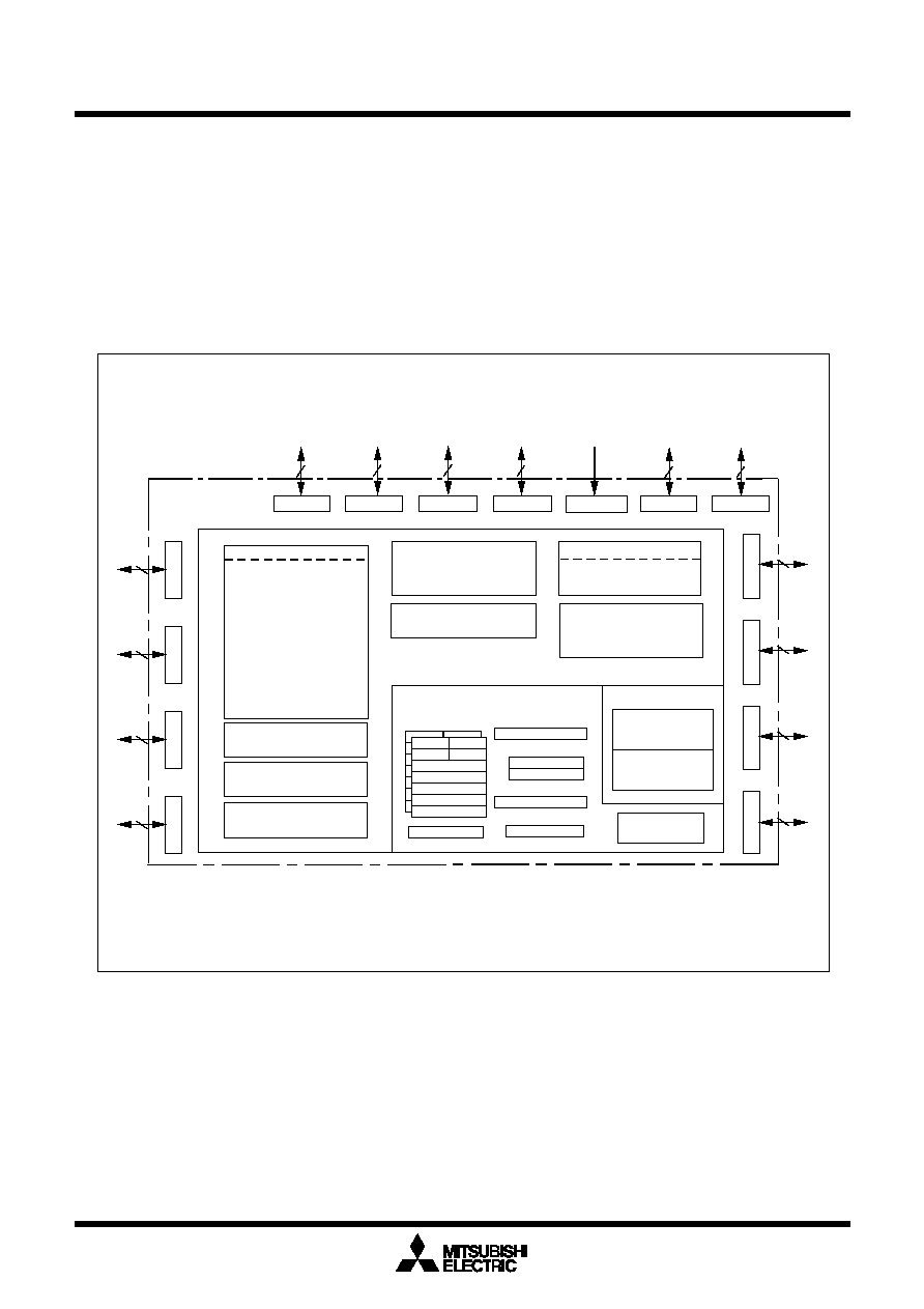
Block Diagram
Figure 1.1.2 is a block diagram of the M30220 group.
Figure 1.1.2. Block diagram of M30220 group
Timer
Internal peripheral functions
Watchdog timer
(15 bits)
Memory
ROM
(Note 1)
RAM
(Note 2)
A-D converter
(10 bits
X
8 channels
UART/clock synchronous SI/O
(8 bits
X
3 channels)
System clock generator
X
IN
-X
OUT
X
CIN
-X
COUT
M16C/60 series 16-bit CPU core
I/O ports
Port P4
8
Port P5
8
Port P6
8
Port P7
7
Port P7
7
1
Port P8
8
R0L
R0H
R1H
R1
L
R
2
R
3
A
0
A
1
FB
R0L
R0H
R1H
R1L
R2
R3
A0
A1
FB
Registers
SB
ISP
USP
Stack pointer
Multiplier
Vector table
INTB
Port P9
8
Flag register
FLG
Program counter
PC
Note 1: ROM size depends on MCU type.
Note 2: RAM size depends on MCU type.
DMAC
(2 channels)
D-A converter
(8 bits X 3 channels)
LCD drive control circuit
(4COM X 48SEG)
Port P10
8
Port P12
8
Port P13
3
Port P3
6
Port P2
8
Port P1
8
Port P0
8
Port P11
8
Timer TA0 (16 bits)
Timer TA1 (16 bits)
Timer TA2 (16 bits)
Timer TA3 (16 bits)
Timer TA4 (16 bits)
Timer TA5 (16 bits)
Timer TA6 (16 bits)
Timer TA7 (16 bits)
Timer TB0 (16 bits)
Timer TB1 (16 bits)
Timer TB2 (16 bits)
Timer TB3 (16 bits)
Timer TB4 (16 bits)
Timer TB5 (16 bits)
Description
Under
development
Preliminary Specifications REV.E
Specifications in this manual are tentative and subject to change.
Mitsubishi microcomputers
M30220 Group
SINGLE-CHIP 16-BIT CMOS MICROCOMPUTER
4
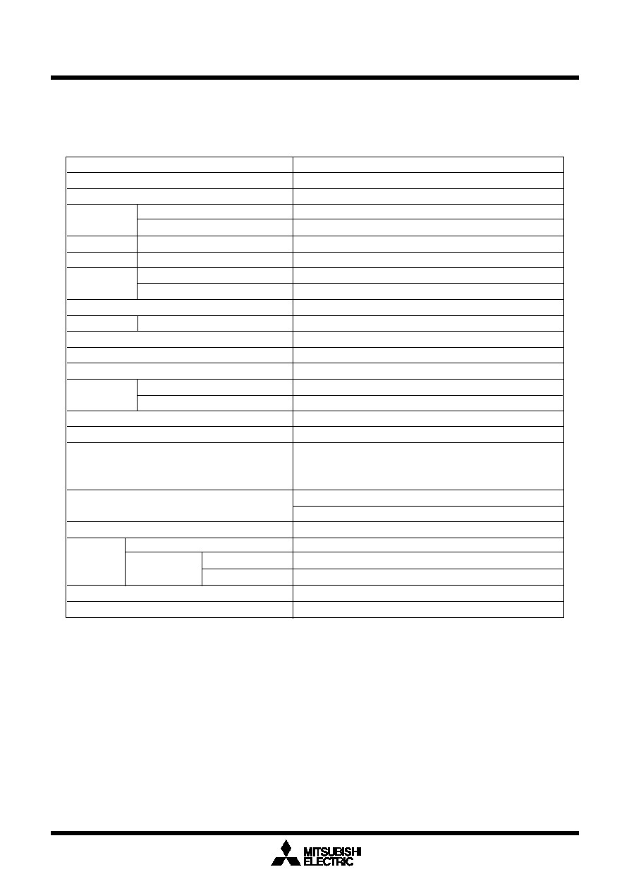
Item
Performance
Number of basic instructions
91 instructions
Shortest instruction execution time
100ns (f(X
IN
)=10MHz
Memory
ROM
96 Kbytes
capacity
RAM
6 Kbytes
I/O port
P0 to P13 (except P7
7
)
8 bits x 11, 3 bits x 1, 6 bits x 1, 7 bits x 1
Input port
P7
7
1 bit x 1
Multifunction
TA0 to TA7
16 bits x 8
timer
TB0 to TB5
16 bits x 6
Real time port outputs
8 bits x 4 lines
Serial I/O
UART0 to UART2
(UART or clock synchronous) x 3
A-D converter
10 bits x 8 channels
D-A converter
8 bits x 3 channels
DMAC
2 channel(trigger:24 sources)
LCD
COM0 to COM3
4 lines
SEG0 to SEG47
48 lines (32 lines are shared with I/O ports)
Watchdog timer
15 bits x 1 (with prescaler)
Interrupt
25 internal and 8 external sources, 4 software sources
Clock generating circuit
2 built-in clock generation circuits
(built-in feedback resistor, and external ceramic or
quartz oscillator)
Supply voltage
4.5V to 5.5V (f(X
IN
)=10MHz)
2.7V to 5.5V (f(X
IN
)=7MHz with software one-wait)
Power consumption
95mW
I/O withstand voltage (P0 to P13)
5 V
Output current P1 to P9,P13
5 mA
P0, P10 to P12
0.1mA("H" output), 2.5mA("L" output)
Device configuration
CMOS silicon gate
Package
144-pin plastic mold QFP
Table 1.1.1. Performance outline of M30220 group
Performance Outline
Table 1.1.1 is performance outline of M30220 group.
I/O char-
acteristics
Under
development
Preliminary Specifications REV.E
Specifications in this manual are tentative and subject to change.
Mitsubishi microcomputers
M30220 Group
SINGLE-CHIP 16-BIT CMOS MICROCOMPUTER
Description
5
Mitsubishi plans to release the following products in the M30220 group:
(1) Support for mask ROM version, flash memory version
(2) ROM capacity
(3) Package
144P6Q-A
: Plastic molded QFP (mask ROM and flash memory versions)
144PFB-A
: Plastic molded QFP(mask ROM and flash memory versions)
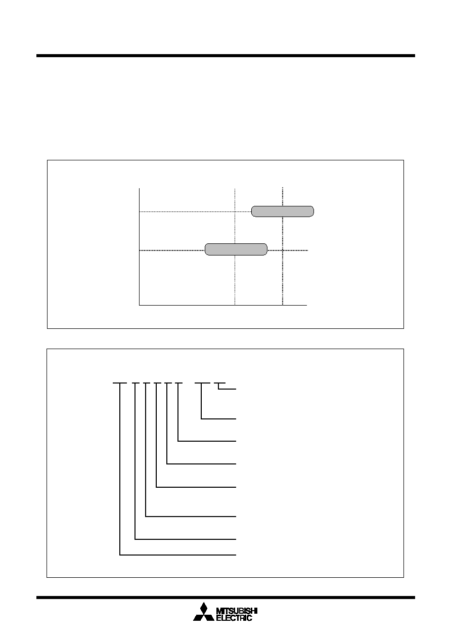
Figure 1.1.3 shows the ROM expansion and figure 1.1.4 shows the Type No., memory size, and package.
Figure 1.1.3. ROM expansion
6K
RAM
(Byte)
96K
ROM
(Byte)
M30220MA-XXXGP/RP
Under development
128K
10K
M30220FCGP/RP
Under development
October. 1999
Figure 1.1.4. Type No., memory size, and package
Type No. M30 22 0 M A - XXX GP
Package type:
GP:
Package144P6Q-A
RP:
144PFB-A
ROM capacity:
A : 96K bytes
C : 128K bytes
ROM No.
Omitted for flash memory version
Memory type:
M : Mask ROM version
F : Flash memory version
Shows RAM capacity, pin count, etc.
(The value itself has no specific meaning)
M16C/22 Group(built-in LCD)
M16C Family
Shows characteristic, use
None: General