 | ÐлекÑÑоннÑй компоненÑ: M30222FG | СкаÑаÑÑ:  PDF PDF  ZIP ZIP |
01 desc Äîêóìåíòàöèÿ è îïèñàíèÿ www.docs.chipfind.ru

1-2
Under
dev
elopment
Specifications in this manual are tentative and subject to change
Rev. G
Description
MITSUBISHI MICROCOMPUTERS
M30222 Group
SINGLE-CHIP 16-BIT CMOS MICROCOMPUTER
Description
The M30222 single-chip microcomputers are built using the high-performance silicon gate CMOS process
using a M16C/60 Series CPU core and are packaged in a 100-pin plastic molded QFP. These single-chip
microcomputers operate using sophisticated instructions featuring a high-level of instruction efficiency and
are capable of executing instructions at high speed. They also feature a built-in multiplier and DMAC,
making them ideal for controlling office, communications, industrial equipment, and other high-speed pro-
cessing applications.
The M30222 group includes a range of products with various package types.
Features
· Memory capacity ......................................... Flash ROM 260 Kbytes
...................................................................... RAM 20 Kbytes
· Shortest instruction execution time ............. 62.5ns (f(X
IN
)=16MH
Z
)
· Supply voltage ............................................ 2.7 to 5.5V
· Low power consumption ............................. TBD
· Interrupts ..................................................... 25 internal and 8 external interrupt sources
4 software interrupt sources
7 levels (including key input interrupt)
· Multifunction 16-bit timer ............................. 5 output timers, 6 input timers, three phase motor control, real-time port
· Serial I/O ..................................................... 5 channel
3 for UART or clock synchronous (1 channel for I
2
C or SPI)
2 for clock synchronous
· DMAC ........................................................... 2 channels (trigger: 24 sources)
· A-D converter ............................................... 10 bits X 8 channels (expandable up to 10 channels)
· D-A converter ............................................... 8 bits X 2 channels
· CRC calculation circuit ................................. 1 circuit
· Watchdog timer ............................................ 1 timer
· Key-on Wake up ........................................... 8 inputs
· Programmable I/O ........................................ 54 lines
· Input port ...................................................... 1 line (P8
3
shared with NMI pin)
· Clock generating circuit ............................... 2 built-in clock generation circuits
(built-in feedback resistor, and external ceramic or quartz oscillator)
·LCD Drive ...................................................... 1/2, 1/3 bias
4 common outputs
40 segment outputs
Built-in charge pump
1/2, 1/3, 1/4 duty
Expansion CLK output
Static/direct drive mode
Applications
Audio, cameras, office, industrial, communications and, portable equipment
Specifications written in this manual
are believed to be accurate but are
not guaranteed to be entirely error
free. They may be changed for func-
tional or performance improvements.
Please make sure your manual is the
latest version.

1-3
Under
dev
elopment
MITSUBISHI MICROCOMPUTERS
M30222 Group
SINGLE-CHIP 16-BIT CMOS MICROCOMPUTER
Specifications in this manual are tentative and subject to change
Rev. G
Description
Table of Contents
Description ............................................................ 1-2
Operation of Functional Blocks ............................ 1-10
Memory ............................................................... 1-10
Central Processing Unit (CPU) ............................ 1-11
Reset ................................................................... 1-14
Special function registers ..................................... 1-15
Software Reset .................................................... 1-20
Clock generating Circuit ...................................... 1-21
Clock Output ........................................................ 1-25
Wait Mode ........................................................... 1-26
Stop Mode ........................................................... 1-27
Status Transition Of BCLK ................................... 1-28
Voltage Down Converter ...................................... 1-30
Power control....................................................... 1-32
Protection ............................................................ 1-34
Software wait ....................................................... 1-35
Overview of Interrupts .......................................... 1-36
Watchdog Timer .................................................. 1-57
DMAC .................................................................. 1-59
Timers ................................................................. 1-69
Timer A ................................................................ 1-71
Timer B ................................................................ 1-85
Timer functions for three-phase motor control ..... 1-93
Serial Communications ...................................... 1-105
(1) Clock synchronous serial I/O mode .............. 1-114
(2) Clock Asynchronous Serial I/O (UART) Mode1-120
UART2 in I2C Mode .......................................... 1-130
UART2 in SPI mode .......................................... 1-138
S I/O 3, 4 ........................................................... 1-143
LCD Drive Control Circuit .................................. 1-147
A-D Converter ................................................... 1-157
D-A Converter .................................................... 1-168
CRC Calculation Circuit ..................................... 1-170
Programmable I/O Ports .................................... 1-172
Electrical Characteristics ................................... 1-179
Flash Memory .................................................... 1-186
CPU Rewrite Mode ............................................ 1-188
Parallel I/O Mode ............................................... 1-202
Standard serial I/O mode 1 ................................ 1-206
Standard serial I/O mode 2 ................................ 1-226
1-4
Under
dev
elopment
Specifications in this manual are tentative and subject to change
Rev. G
Description
MITSUBISHI MICROCOMPUTERS
M30222 Group
SINGLE-CHIP 16-BIT CMOS MICROCOMPUTER
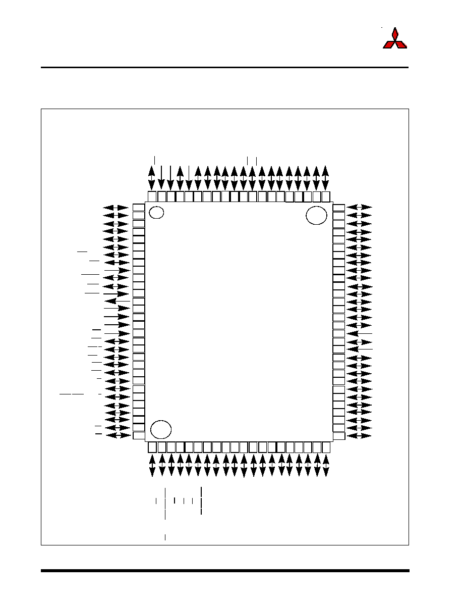
Pin Configuration
Figure 1.1 shows the pin configurations for M30222 group.
Fig. 1.1. Pin configuration (top view)
91
85
86
87
88
89
90
92
93
94
95
96
97
98
99
81
82
83
84
100
40
2
1
SEG30/P
3
6
VL3
P74/TA2OUT/W
46
24
VL1
CO
M2
P107/A
N
7/INT7
P106/AN
6
/INT6
P1
05/AN5
P1
04/AN4
P10
3
/AN3
P10
2
/AN2
P101/AN
1
AV
s
s
P10
0
/AN0
Vref
AV
cc
P97
/
ADtrg/L
E
D7/Sin4
/INT3
P75/TA2IN/W
23
P76/TA3OUT/INT4
22
P77/TA3IN/INT4
21
P80/TA4OUT/INT5/U
20
P82/INT0
19
P81/TA4IN/INT5/U
18
P83/NMI
17
V
cc
16
Xin
15
Vss
14
Xout
13
RESET
12
11
P85/Xcin
10
CNVss
9
P86/INT1
8
P90/TB0in/INT2/CLK3
7
P91/TB1in/Sin3
6
P92/TB2in/Sout3
5
P93/DA0/TB3in
4
P94/DA1/TB4in
3
P95/ANEX0/CLK4
P96/ANEX1/Sout4
SEG31/P
3
7
45
SEG32
/P40
44
SEG33/P
4
1
43
SEG34
/P42
42
SEG35/P
4
3
41
SEG36/P
4
4
SEG37/P
4
5
39
38
37
P6
0
/
C
T
S
0
/RTS0
/K
I0
36
P61/CLK
0
/KI1
35
P62/RxD0/KI2
34
P63/TxD0/KI3
33
P64/C
T
S1
/RTS
1
/CTS0
/C
LKS1/K
I4
32
P65/CL
K1/KI5
M30222FG
P67/TxD1/KI7
29
P70/TxD2/SDA/TA0OUT
28
P71/RxD2/SCL/TA0IN/TB5IN
27
P72/CLK2/TA1OUT/V
26
P73/CTS2/RTS2/TA1IN/V
25
P66/RxD1/KI6
30
SEG2
6
/P32
50
SEG27
/P33
49
SEG28
/P34
48
SEG29/
P35
47
COM1
COM0
C2
C1
P84/Xcout
SEG
3
8/P46/R
T
P0
SEG39/
P47/RTP
1
VL2
79
80
57
58
59
60
61
62
63
64
65
66
67
68
69
70
71
72
73
74
75
76
77
78
52
53
54
55
56
51
31
SEG19
SEG18
SEG17
SEG16
SEG15
Vcc
SEG14
Vss
SEG13
SEG12
SEG11
SEG10
SEG09
SEG08
SEG07
SEG06
SEG05
SEG04
SEG03
SEG02
SEG01
SEG00
COM3
SEG25/P31
SEG24/P30
SEG23
SEG22
SEG21
SEG20
VDC
1-5
Under
dev
elopment
MITSUBISHI MICROCOMPUTERS
M30222 Group
SINGLE-CHIP 16-BIT CMOS MICROCOMPUTER
Specifications in this manual are tentative and subject to change
Rev. G
Description
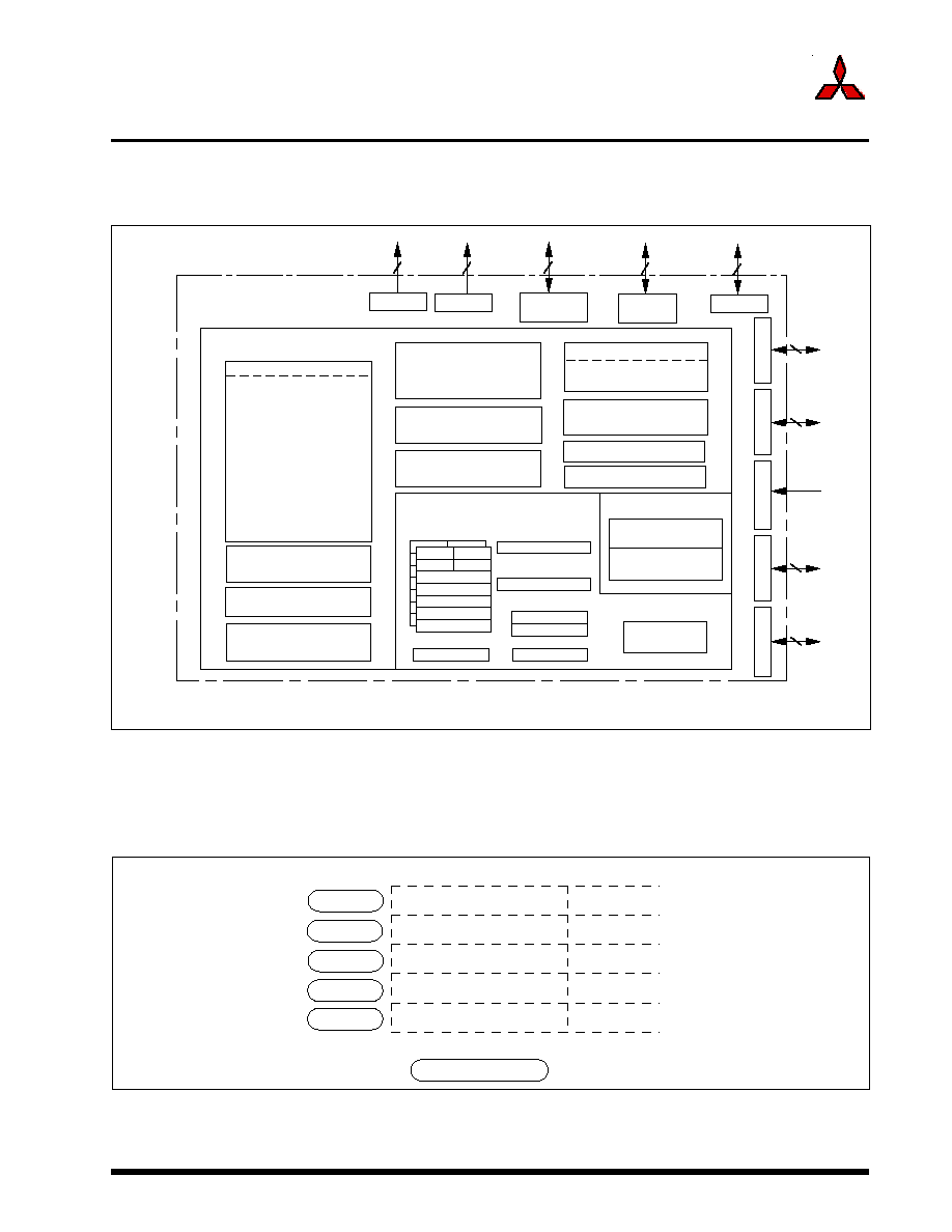
Block Diagram
Figure 1.2 is a block diagram of the M30222 group.
Fig. 1.2. Block diagram of M30222 group
Timer
Timer TA0 (16 bits)
Timer TA1 (16 bits)
Timer TA2 (16 bits)
Timer TA3 (16 bits)
Timer TA4 (16 bits)
Timer TB0 (16 bits)
Timer TB1 (16 bits)
Timer TB2 (16 bits)
Timer TB3 (16 bits)
Timer TB4 (16 bits)
Timer TB5 (16 bits)
Internal peripheral functions
Watchdog timer
(15 bits)
DMAC
(2 channels)
D-A converter
(8 bits X 2 channels)
A-D converter
(10 bits
X
8 channels
Expandable up to 10 channels)
UART/clock synchronous SI/O
(8 bits
X
3 channels)
System clock generator
X
IN
-X
OUT
X
CIN
-X
COUT
M16C/60 series16-bit CPU core
I/O ports
COM 0-3
4
SEG 0-23
24
Port P3
SEG 24-31
8
Port P4
SEG 32-39
8
Port P6
8
R0L
R0H
R1H
R1L
R2
R3
A0
A1
FB
R0L
R0H
R1H
R1L
R2
R3
A0
A1
FB
Registers
ISP
USP
Stack pointer
Vector table
INTB
CRC arithmetic circuit (CCITT )
(Polynomial : X
16
+X
12
+X
5
+1)
Multiplier
P
o
r
t
P10
P
o
r
t
P9
P
o
r
t
P8
P
o
r
t
P7
Memory
P
o
r
t
P8
3
ROM
(Note 1)
RAM
(Note 2)
Note 1: ROM size depends on MCU type.
Note 2: RAM size depends on MCU type.
SB
FLG
PC
Program counter
Clock synchronous SI/O
(8 bits
X
2 channels)
VDC
LCD Controller
8
8
8
1
6
Memory Expansion
Figure 1.3 shows the Memory expansion for the M30222 group.
Fig. 1.3. Memory Expansion
M30222FC/FP/GP
ROM size
(Bytes)
260K
128K
96K
64K
32K
20K SRAM
Flash Memory Version
1-6
Under
dev
elopment
Specifications in this manual are tentative and subject to change
Rev. G
Description
MITSUBISHI MICROCOMPUTERS
M30222 Group
SINGLE-CHIP 16-BIT CMOS MICROCOMPUTER
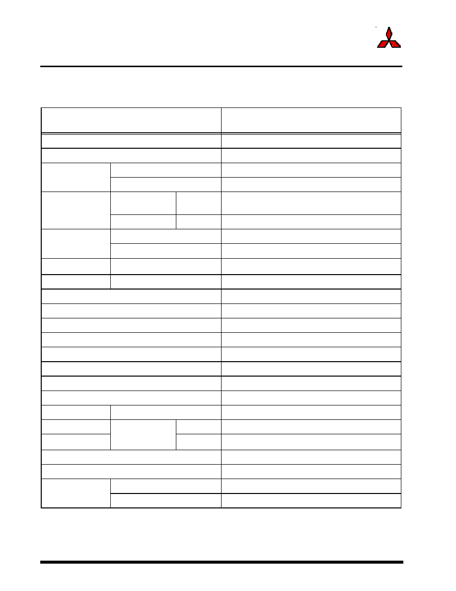
Performance Outline
Table 1.1. Performance outline of the M30222 group
Parameters
Functions
Number of basic instructions
91
Shortest instruction execution time
62.5ns f(Xin) = 16MHz
Memory size
ROM
260K bytes
RAM
20K bytes
Input/Output
P3-P4, P6-P10
except P83
I/O
8 bits x 6, 7 bits x 1
P83
I
1 bit x 1
Multifunctional
timer
TA0, TA1, TA2, TA3, TA4
16 bits x 5
TB0, TB1, TB2, TB3, TB4, TB5
16 bits x 6, three-phase motor control
Serial I/O
UART0, UART1, UART2
(UART or clock synchronous) x 3, or I
2
C x 1
SIO3, SIO4
(Clock synchronous) x 2
A-D converter
10 bits x (8 + 2) channels
D-A converter
8 bits x 2
CRC calculation circuit
CRC-CCITT
Watchdog timer
15 bits x 1 (with prescaler)
Interrupts
25 external, 8 internal sources, 4 software, 7 levels
Clock generating circuit
2 built-in clock generation circuits
Supply voltage
2.7 to 5.5V f(Xin) = 16 MHz, without software wait
Power consumption
TBD
I/O characteristics
I/O withstand voltage
5.5V
Output current
P3, P4
0.1 mA (high output), 2.5 mA (low output)
P6-P10
5 mA at 5V (excluding pins P7
0
, P7
1
, P8
3
)
Device configuration
CMOS high performance silicon gate
Package
100-pin plastic mold QFP
LCD
COM0 to COM3
4 lines
SEG0 to SEG39
40 lines (16 lines shared with I/O ports)
Document Outline
- Description
- Pin Configuration
- Performance Outline
- Pin Description
- Memory
- Operation of Functional Blocks
- Central Processing Unit
- Reset
- Special function registers
- Software Reset
- Clock generating Circuit
- Clock Output
- Wait Mode
- Stop Mode
- Voltage Down Converter
- Power control
- Software wait
- Protection
- Interrupts
- Interrupt Vector Tables
- Variable vector tables
- Interrupt Control
- Interrupt Sequence
- Saving Registers
- INT Interrupt
- NMI Interrupt
- Address Match Interrupt
- Precautions for Interrupts
- Watchdog Timer
- DMAC
- Transfer cycle
- DMAC transfer cycles
- DMA enable bit
- DMA request bit
- Timers
- Timer A
- Timer mode
- Event counter mode
- One-shot timer mode
- Pulse width modulation (PWM) mode
- Real-time port mode
- Timer B
- Timer mode
- Event counter mode
- Pulse period/pulse width measurement mode
- Timer functions for three-phase motor control
- Delta modulation
- Sawtooth modulation
- Serial Communications
- UART0 to 2
- Clock synchronous serial I/O mode
- Polarity select function
- LSB first/MSB first select function
- Transfer clock output from multiple pins function (UART1)
- Continuous receive mode
- Separate CTS/RTS pins function (UART0)
- Serial data logic switch function (UART2)
- Clock Asynchronous Serial I/O (UART) Mode
- Separate CTS/RTS pins function (UART0)
- Sleep mode (UART0, UART1)
- Function for switching serial data logic (UART2)
- TxD, RxD I/O polarity reverse function (UART2)
- Bus collision detection function (UART2)
- Clock-asynchronous serial I/O mode (compliant with the SIM interface)
- Function for outputting a parity error signal
- Direct format/inverse format
- UART2 in I 2 C Mode
- UART2 Special Mode Register 2
- UART2 in SPI mode
- SPI operation
- Master Mode operation
- Slave mode operation
- S I/O 3, 4
- LCD Drive Control Circuit
- Voltage Multiplier
- Bias Control and Applied Voltage to LCD Power Input Pins
- Common Pin and Duty Control
- LCD Display RAM
- LCD Drive Timing
- LCD Static Drive
- LCD Expansion Clock
- A-D Converter
- One-shot mode
- Repeat mode
- Single sweep mode
- Repeat sweep mode 0
- Repeat sweep mode 1
- Sample and hold
- Extended analog input pins
- External operation amp connection mode
- Operation of Simultaneous Sample and Hold Mode (SSH)
- A-D Usage Precautions
- D-A Converter
- CRC Calculation Circuit
- Programmable I/O Ports
- Electrical Characteristics
- Flash Memory
- Outline Performance
- CPU Rewrite Mode
- Microcomputer Mode and Boot Mode
- Block Address
- Outline Performance
- Precautions on CPU Rewrite Mode
- Software Commands
- Status Register
- Functions to Inhibit Rewriting Flash Memory Version
- ROM code protect register
- ID Code Check Function
- Parallel I/O Mode
- User ROM and Boot ROM Areas
- Standard serial I/O mode
- Serial I/O Mode 1
- Serial I/O Mode 2
- Overview of standard serial I/O mode 1 (clock synchronous)
- Example Circuit Application for the Standard Serial I/O Modes 1 and 2
- Standard serial I/O mode 2 (clock asynchronized)