
MITSUBISHI ELECTRONICS
AMERICA, INC.
PRELIMINARY
M30240
M30240 Group Specification
Description. . . . . . . . . . . . . . . . . . . . . . . . . . . . 1-3
Features...............................................................1-3
Applications......................................................... 1-3
Pin Configuration ................................................ 1-4
Block Diagram..................................................... 1-5
Performance outline............................................ 1-6
Pin Description.................................................... 1-8
Overview ........................................................... 1-10
Operation of Functional Blocks . . . . . . . . . 1-11
Central Processing Unit (CPU) ......................... 1-11
Processor Mode................................................ 1-14
Memory ............................................................. 1-15
SFR MAP .......................................................... 1-16
Reset................................................................. 1-22
Software Reset ................................................. 1-23
Clock-Generating Circuit................................... 1-23
Clock Control .................................................... 1-24
Stop Mode......................................................... 1-26
Wait Mode......................................................... 1-26
Status Transition Of the Internal Clock
......... 1-26
Power Control ................................................... 1-27
Protection.......................................................... 1-28
Interrupts........................................................... 1-29
NMI Interrupt ..................................................... 1-35
Key-Input Interrupt ............................................ 1-36
Address Match Interrupt.................................... 1-38
Watchdog Timer................................................ 1-39
Frequency Synthesizer Circuit .......................... 1-41
Universal Serial Bus.......................................... 1-44
DMAC ............................................................... 1-63
Timers ............................................................... 1-68
Timer A ............................................................. 1-69
Timer B ............................................................. 1-80
UART0 through UART2 .................................... 1-83
A-D Converter ................................................. 1-106
CRC Calculation Circuit .................................. 1-116
Programmable I/O Ports ................................. 1-117
Usage. . . . . . . . . . . . . . . . . . . . . . . . . . . . . 1-124
Usage Precautions.......................................... 1-124
Specifications . . . . . . . . . . . . . . . . . . . . . . 1-128
Electrical ......................................................... 1-128
Timing ............................................................. 1-130
Timing Diagrams- Peripheral/interrupt ............ 1-133
Applications . . . . . . . . . . . . . . . . . . . . . . . 1-134
Frequency Synthesizer Interface
and DC-DC Converter..................................... 1-134
Attach/Detach Function................................... 1-138
Low Pass Filter Network ................................. 1-139
USB Transceiver............................................. 1-140
Programming Notes ........................................ 1-141

MITSUBISHI ELECTRONICS
AMERICA, INC.
1-2

1-3
Mitsubishi microcomputers
M30240 Group
SINGLE-CHIP 16-BIT CMOS MICROCOMPUTER
Preliminary Specifications REV. E
Specifications in this manual are tentative and subject to change
Features
1.0 Description
The M30240 group is a 16-bit microcomputer based on the M16C family core technology. They are
single-chip USB peripheral microcontrollers based on the Universal Serial Bus (USB) Version 1.1
specification. They are packaged in an 80-pin, molded plastic QFP. These single-chip microcontrollers
operate using sophisticated instructions featuring a high level of instruction efficiency, making them
capable of executing instructions at high speed. They also feature a built-in multiplier and DMAC,
making them ideal for controlling office communications, industrial equipment, and other high-speed
processing applications.
1.1 Features
� CPU .................................................... 16-bit (including a hardware multiplier)
� Number of instructions ........................ 91
� Shortest instruction execution time ..... 83ns f(X
IN
)=12MHz
� USB Features:..................................... Five endpoint pairs (IN/OUT)
FIFO Sizes (endpoints 0-4):32,128, 32, 32, 32
Conforms to USB V1.1 Specification
� USB Transceiver ................................. Conforms to USB V1.1 Specification-Internal Vref
� Frequency Synthesizer........................ PLL for 48MHz clock
� Memory capacity (mask device):......... ROM (40K, 48K) / RAM (3.0 K)
� Memory capacity (OTP device): .......... PROM (128K) / RAM (5K)
� Supply Voltage .................................... 4.1 to 5.25V f(X
IN
)=12MHz)
� Interrupts............................................. 21 internal and 4 external interrupt sources,
4 software interrupt sources; 7 levels (including key input interrupt X 16)
� Multifunction timer ............................... 5 X 16-bit, w/integrated 20mA (peak) PWM outputs
� General purpose timer ........................ 3 X 16-bit, internal interrupt only
� UART................................................... 3 X 7/8/9 bits;
Configurable for synchronous or asynchronous mode
� DMAC.................................................. 2 channels (trigger: 18 sources)
� A-D Converter ..................................... 10 bits X 8 channels
� CRC calculation circuit ........................ 1 circuit (industry standard polynomial)
� Watchdog timer ................................... 1 line (15 bit)
� Programmable I/O ............................... 63 lines
� High current and LED Drivers ............. 5 high current and 8 LED drivers
� Clock-generating circuit....................... 1 built-in circuit including feedback resistor
� Package: ............................................. 80P6N (0.8 mm pitch)
1.2 Applications
USB peripherals, such as telephones, audio systems, scanners, and digital cameras.
1-4
Mitsubishi microcomputers
M30240 Group
SINGLE-CHIP 16-BIT CMOS MICROCOMPUTER
Preliminary Specifications REV. E
Specifications in this manual are tentative and subject to change
Pin Configuration
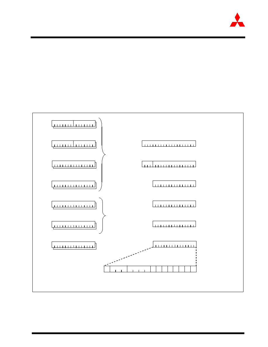
1.3 Pin Configuration
Figure 1.1 shows the pin configuration (top view).
Figure 1.1:
Pin Configuration (top view)
41
40
24
65
P100/AN0
66
AVss
67
LPF
68
Vref
69
AVcc
70
P87/
AD
TRG
71
P86/SOF
72
EXTCAP
73
74
75
76
77
78
79
80
23
22
21
20
19
18
17
16
15
P84/INT1
14
P85/
NMI
13
Vcc
12
11
10
Xin
9
Vss
8
Xout
7
6
D-
5
D+
4
3
2
1
39
38
37
36
35
34
33
32
31
30
29
28
27
26
25
42
43
44
45
46
47
48
49
50
51
52
53
54
55
56
57
58
59
60
P107/AN7
P106/AN6
P105/AN5
M30240Mx/EC
RESET
61
P104/AN4
62
P103/AN3
63
P102/AN2
64
P101/AN1
P83/A
TT
A
C
H
P82/INT0
P81/T
A4IN
P80/T
A4OUT
P77/T
A3IN
P75/T
A2IN
P72/CLK2/T
A1OUT
P73/
CTS2/RTS2
/T
A1IN
P74/T
A2OUT
P76/T
A3OUT
P32
P33
P34
P35
P36
P37/CLKout
P60/CTS0/RTS0
P61/CLK0
P62/RxD0
P63/TxD0
P64/
CTS1/RTS1/CLKS1
P65/CLK1
P66/RxD1
P67/TxD1
P70/TxD2/TA0OUT
P71/RxD2/TA0IN
P03/KI3
P02/KI2
P01/KI1
P00/KI0
P04/
KI4
P05/
KI5
P06/
KI6
P07/
KI7
P10/
KI8
P11
/KI9
P12/
KI10
P13/
KI11
P14/
KI12
P15/
KI13
P16/
KI14
Vss
P17/
KI15
Vcc
P20/LED0
P21/LED1
P22/LED2
P23/LED3
P24/LED4
P25/LED5
P26/LED6
P27/LED7
P30
P31
BYTE
CNVss

1-5
Mitsubishi microcomputers
M30240 Group
SINGLE-CHIP 16-BIT CMOS MICROCOMPUTER
Preliminary Specifications REV. E
Specifications in this manual are tentative and subject to change
Block Diagram
1.4 Block Diagram
Figure 1.2 is a block diagram of the M30240 group.
Figure 1.2:
Block diagram of M30240 group
Timer
Timer TA0 (16 bits)
Timer TA1 (16 bits)
Timer TA2 (16 bits)
Timer TA3 (16 bits)
Timer TA4 (16 bits)
Timer TB0 (16 bits)
Timer TB1 (16 bits)
Timer TB2 (16 bits)
Internal peripheral functions
Watchdog timer
(1 line)
DMAC
(2 channels)
A-D converter
10 bits
X
8 channels
UART/clock synchronous SI/O
(8 bits
X
3 channels)
(Note 1)
System clock generator
X
IN
-X
OUT
I/O ports
CRC arithmetic circuit (CCITT)
(Polynomial : X
16
+X
12
+X
5
+1)
Note 1: One of serial I/O can be used for SIM interface.
Memory
ROM
RAM
M16C series16-bit CPU core
R0L
R0H
R0L
R0H
R1H
R1L
R2
R3
A0
A1
FB
Registers
ISP
USP
Stack pointer
Vector table
INTB
Multiplier
SB
FLG
PC
Program counter
Port P0
8
Port P1
8
Port P2
8
Port P3
8
Port P6
8
Port P7
8
Port P80~84
86, 87
7
Port P8
5
Port P10
8
USB function
Frequency Synthesizer
1-6
Mitsubishi microcomputers
M30240 Group
SINGLE-CHIP 16-BIT CMOS MICROCOMPUTER
Preliminary Specifications REV. E
Specifications in this manual are tentative and subject to change
Performance outline
1.5 Performance outline
Table 1.1 is a performance outline of the M30240 group.
Table 1.1:
Performance outline of M30240 group
Item
Performance
Number of basic instructions
91 instructions
Shortest instruction execution time
83ns (f(X
IN
) =12MHz)
Memory capacity
ROM
(See Figure 3: ROM capacity field)
RAM
I/O port
P0 to P3, P6,P7, P8
(except P85), P10
8 bits x 7, 7 bits x 1
Input port
P85
1 bit x 1
Multifunction Timer
TA0, TA1, TA2, TA3, TA4
16 bits x 5
General purpose Timer
TB0, TB1, TB2
16 bits x 3
Serial I/O
UART0, UART1, UART2
(UART or clock synchronous) x 3
A-D converter
10 bits x 8 channels
DMAC
2 channels (trigger:18 sources)
CRC calculation circuit
CRC-CCITT
Watchdog timer
15 bits x 1 (with prescaler)
Interrupt
21 internal and 4 external sources, 4 software sources, 7 levels
Clock-generating circuit
Built-in clock generation circuit (built-in feedback resistor, and
external ceramic or quartz oscillator)
Supply voltage (typical)
4.1 to 5.25V, (f(X
IN
)=12MHz, without software wait)
Power consumption (typical)
250 mwatt, Vcc=5.0V, 12MHz
I/O characteristics
I/O withstand voltage
5V
Average output current
5 mA available on ports P0, P1, P3,P6, P7
1
, P7
3
, P7
5
, P7
7
,
P8
1
~P8
4
, P8
6
, P8
7
, P10
10 mA available on ports P2, P7
0
, P7
2
, P7
4
, P7
6
, P8
0
Operating temperature
0 to 70
o
C
Device configuration
CMOS high performance silicon gate
Package
80-pin plastic molded QFP

1-7
Mitsubishi microcomputers
M30240 Group
SINGLE-CHIP 16-BIT CMOS MICROCOMPUTER
Preliminary Specifications REV. E
Specifications in this manual are tentative and subject to change
Performance outline
Mitsubishi plans to release the following products in the M30240 group:
(1) Support for mask ROM version and one-time PROM version
(2) ROM capacity
(3) Package
�
80P6N: Plastic molded QFP (mask ROM version and one-time PROM version)
Figure 1.3 shows the type number, memory size and package for the M30240 group.
Figure 1.3:
Type number, memory size, and package
Table 1.2 shows the Package Number, type, ROM and RAM Capacity for M30240 Group.
Table 1.2:
M30240 Group
Type
ROM Capacity
RAM Capacity
Package Type
Remarks
M30240M5
40K bytes
3K bytes
80P6N
Mask ROM Version
M30240M6
48K bytes
3K bytes
80P6N
Mask ROM Version
M30240ECFP
128K bytes
5K bytes
80P6N
One-time PROM version
Package type:
FP : Package
80P6N
ROM No.
Omitted for blank one-time PROM version,and
EPROM version
ROM capacity:
1: 8K bytes
7: 56K bytes
2: 16K bytes
8: 64K bytes
3: 24K bytes
9: 80K bytes
4: 32K bytes
A: 96K bytes
5: 40K bytes
C: 128K bytes
6: 48K bytes
Memory type:
M : Mask ROM version
E : EPROM or one-time PROM version
S : External ROM version
F : Flash memory version
Type No. M 3 0 24 0 M 5 � X X X F P
M30240 Group
M16C Family
Part type:
Specifies part variations with M30240 group

1-8
Mitsubishi microcomputers
M30240 Group
SINGLE-CHIP 16-BIT CMOS MICROCOMPUTER
Preliminary Specifications REV. E
Specifications in this manual are tentative and subject to change
Pin Description
1.6 Pin Description
Table 1.3:
Figure Pin Description
Pin #
Name
I/O
Description
1
P8
7
I/O
CMOS I/O port. This pin also functions as an external trigger for A-D conversion.
2
P8
6
I/O
CMOS I/O port. This pin also functions as the start of frame (SOF) pulse for the
USB module.
3
P8
5
/(NMI)
I
CMOS input port. This pin also functions as a non-maskable external interrupt.
4,5
P8
4
~ P8
3
I/O
CMOS I/O port. These pins also functions as external interrupt 1 and are used
to enable the stealth detach function for the USB transceiver.
6
EXTCAP
_
An external capacitor (Ext. Cap) pin. When the USB transceiver voltage
converter is used, a 2.2
�
F and a 0.1
�
F capacitor should connect between this
pin and V
ss
to ensure proper operation of the USB line driver. This option is
enabled by setting bit 4 of the USB control register (000C
16
) to a "1".
7
BYTE
I
Connect this pin to Vss
8
CNV
ss
I
Connect this pin to Vss
9
USB D
+
I/O
USB D+ voltage line interface, a series resistor of 33
is connected to this pin.
10
USB D
-
I/O
USB D- voltage line interface, a series resistor of 33
is connected to this pin.
11
RESET
I
A "L" on this input resets the microcomputer.
12
Xout
O
See Xin
13
V
ss
I
Ground: V
ss
= 0V
14
Xin
I
Input and output signals to and from the internal clock generation circuit.
Connect a ceramic resonator or quartz crystal between Xin and Xout pins to set
the oscillation frequency. If an external clock is used, connect the clock source
to the Xin pin and leave the Xout pin open.
15
V
cc
I
Power: V
cc
= 4.1~ 5.25V
16
P8
2
I/O
CMOS I/O port. This pin also functions as external interrupt 0.
17-18
P8
1
~ P8
0
I/O
CMOS I/O port. Pins in this port also function as TimerA4 input and output as
selected by software.
19-22
P7
7
~ P7
4
I/O
CMOS I/O port. Pins in this port also function as timer pins.
P7
7
and P7
6
can function as TimerA3 input and output as selected by software.
P7
5
and P7
4
can function as TimerA2 input and output as selected by software.
23-26
P7
3
~ P7
0
I/O
CMOS I/O port. Pins in this port also function as UART2 CTS, RTS, CLK, RXD,
and TXD as selected by software.
P7
3
and P7
2
can function as TimerA1 input and output as selected by software.
P7
1
and P7
0
can function as TimerA0 input and output as selected by software.
27-30
P6
7
~ P6
4
I/O
CMOS I/O port. Pins in this port also function as UART1 CTS, RTS, CLK, Serial
Clock, RXD, and TXD as selected by software. TXD(OE~) and RTS(SUSPEND)
in addition to D+ and D- can be used to run the device in USB bypass mode.
31-34
P6
3
~ P6
0
I/O
CMOS I/O port. Pins in this port also function as UART0 CTS, RTS, CLK, RXD,
and TXD as selected by software.
35-42
P3
7
~ P3
0
I/O
CMOS I/O port.
43-50
P2
7
/LED7
~ P2
0
/LED0
I/O
CMOS I/O port. These pins are capable of driving up to 20mA (peak) for LEDs.
1-9
Mitsubishi microcomputers
M30240 Group
SINGLE-CHIP 16-BIT CMOS MICROCOMPUTER
Preliminary Specifications REV. E
Specifications in this manual are tentative and subject to change
Pin Description
51
V
cc
I
Power: V
cc
= 4.1~ 5.25V
52
P1
7
/KI
15
I/O
CMOS I/O port. This port can also function as the key-on wakeup interrupt KI15.
53
V
ss
I
Ground: V
ss
= 0V
54-60
P1
6
/KI
14
~ P1
0
/KI
8
I/O
CMOS I/O port. This port can also function as the key-on wakeup interrupts (KI8
~ KI14).
61-68
P0
7
/KI
7
~ P0
0
/KI
0
I/O
CMOS I/O port. This port can also function as the key-on wakeup interrupts (KI0
~ KI7).
69-76
P10
7
~ P10
0
I/O
CMOS I/O port. These pins also function as Analog inputs 7-0 for A-D
conversion
77
AV
ss
I
This pin is a power supply input for the AD converter. (Connect to Vss)
78
LPF
O
Loop filter for the frequency synthesizer.
79
V
REF
I
This pin is the reference voltage input for the A-D converter.
80
AV
cc
I
This pin is a power supply input for the AD converter. (Connect to Vcc)
Table 1.3:
Figure Pin Description
Pin #
Name
I/O
Description
1-10
Mitsubishi microcomputers
M30240 Group
SINGLE-CHIP 16-BIT CMOS MICROCOMPUTER
Preliminary Specifications REV. E
Specifications in this manual are tentative and subject to change
Overview
1.7 Overview
The M30240 group is a single chip PC peripheral microcontroller based on the Universal
Serial Bus (USB) Version 1.1 specification. This device provides interface between a USB-
equipped host computer and PC peripherals such as telephones, audio systems, and digital
cameras. The M30240 block diagram is shown in Figure 1.4.
The USB function control unit of the M30240 group can support all four data transfer types
listed in the USB specification: Isochronous, Interrupt, Bulk, and Control. Each transfer type is
used for controlling a different set of PC peripherals. Isochronous transfers provide guaranteed
bus access, a constant data rate, and error tolerance for devices such as computer-telephone
integration (CTI) and audio systems. Interrupt transfers are designed to support human input
devices (HID) that communicate small amounts of data infrequently. Bulk transfers are
necessary for devices such as digital cameras and scanners that communicate large amounts
of data to the PC as bus bandwidth becomes free. Finally, control transfers are supported
and are useful for bursty, host-initiated type communication where bus management is the
primary concern.
Figure 1.4:
M30240 block diagram
frequency
RAM
DMAC x 2
M16C CPU
UART x 3
Timers x 8
Watchdog
CRC Circuit
I/O Ports (P0~P3, P6 ~ P8, P10)
FIFOs
USB Function Control Unit
T
ranscei
v
e
r
D+
D-
(Normal MCU or DMA Transfer)
1 - 12MHz
48 MHz
synthesizer
LED Drivers
(X 8)
A-D
Converter
Timer
ROM
1-11
Mitsubishi microcomputers
M30240 Group
SINGLE-CHIP 16-BIT CMOS MICROCOMPUTER
Preliminary Specifications REV. E
Specifications in this manual are tentative and subject to change
Central Processing Unit (CPU)
2.0 Operation of Functional Blocks
The M30240 group accommodates certain units in a single chip. These units include ROM and RAM to
store instructions and data, and the central processing unit (CPU) to execute arithmetic/logic operations.
Also included are peripheral units such as USB, timers, serial I/O, DMAC, CRC calculation circuit, A-D
converter, and I/O ports.
The following explains each unit.
2.1 Central Processing Unit (CPU)
The CPU has a total of 13 registers shown in Figure 1.5. Seven of these registers (R0, R1, R2, R3, A0,
A1, and FB) come in two sets; therefore, these have two register banks.
Figure 1.5:
Central processing unit register
2.1.1 Data registers (R0, R0H, R0L, R1, R1H, R1L, R2, and R3)
Data registers (R0, R1, R2, and R3) are configured with 16 bits, and are used primarily for transfer
and arithmetic/logic operations.
H
L
b15
b8
b7
b0
R0
(Note)
H
L
b15
b8
b7
b0
R1
(Note)
R2
(Note)
b15
b0
R3
(Note)
b15
b0
A0
(Note)
b15
b0
A1
(Note)
b15
b0
FB
(Note)
b15
b0
Data
registers
Address
registers
Frame base
registers
b15
b0
b15
b0
b15
b0
b15
b0
b0
b19
b0
b19
H
L
Program counter
Interrupt table
register
User stack pointer
Interrupt stack
pointer
Static base
register
Flag register
PC
INTB
USP
ISP
SB
FLG
Note: These registers consist of two register banks.
C
D
Z
S
B
O
I
U
IPL

1-12
Mitsubishi microcomputers
M30240 Group
SINGLE-CHIP 16-BIT CMOS MICROCOMPUTER
Preliminary Specifications REV. E
Specifications in this manual are tentative and subject to change
Central Processing Unit (CPU)
Registers R0 and R1 each can be used as separate 8-bit data registers, high-order bits as (R0H/R1H),
and low-order bits as (R0L/R1L). In some instructions, registers R2 and R0, as well as R3 and R1, can
be used as 32-bit data registers (R2R0/R3R1).
2.1.2 Address registers (A0 and A1)
Address registers (A0 and A1) are configured with 16 bits, and have functions equivalent to those of
data registers. These registers can also be used for address register indirect addressing and address
register relative addressing.
In some instructions, registers A1 and A0 can be combined for use as a 32-bit address register (A1A0).
2.1.3 Frame base register (FB)
Frame base register (FB) is configured with 16 bits, and is used for FB relative addressing.
2.1.4 Program counter (PC)
Program counter (PC) is configured with 20 bits, indicating the address of an instruction to be execut-
ed.
2.1.5 Interrupt table register (INTB)
Interrupt table register (INTB) is configured with 20 bits, indicating the start address of an interrupt vec-
tor table. INTB can be used as separate registers of four high-order bits and 16 low-order bits.
2.1.6 Stack pointer (USP/ISP)
Stack pointer comes in two types: user stack pointer (USP) and interrupt stack pointer (ISP), each con-
figured with 16 bits.
Your desired type of stack pointer (USP or ISP) can be selected by a stack pointer select flag (U flag).
This flag is located at the position of bit 7 in the flag register (FLG).
2.1.7 Static base register (SB)
Static base register (SB) is configured with 16 bits, and is used for SB relative addressing.
2.1.8 Flag register (FLG)
Flag register (FLG) is configured with 11 bits, each bit is used as a flag. Figure 1.6 shows the flag reg-
ister (FLG). The following explains the function of each flag:
2.1.8.1 Bit 0: Carry flag (C flag)
This flag retains a carry, borrow, or shift-out bit that has occurred in the arithmetic/logic unit.
2.1.8.2 Bit 1: Debug flag (D flag)
This flag enables a single-step interrupt.
When this flag is "1", a single-step interrupt is generated after instruction execution. This flag is cleared to "0"
when the interrupt is acknowledged.
2.1.8.3 Bit 2: Zero flag (Z flag)
This flag is set to "1" when an arithmetic operation resulted in 0; otherwise, cleared to "0".
2.1.8.4 Bit 3: Sign flag (S flag)
This flag is set to "1" when an arithmetic operation resulted in a negative value; otherwise, cleared to "0".
2.1.8.5 Bit 4: Register bank select flag (B flag)
This flag chooses a register bank. Register bank 0 is selected when this flag is "0"; register bank 1 is selected
when this flag is "1".
2.1.8.6 Bit 5: Overflow flag (O flag)
This flag is set to "1" when an arithmetic operation resulted in overflow; otherwise, cleared to "0".

1-13
Mitsubishi microcomputers
M30240 Group
SINGLE-CHIP 16-BIT CMOS MICROCOMPUTER
Preliminary Specifications REV. E
Specifications in this manual are tentative and subject to change
Central Processing Unit (CPU)
2.1.8.7 Bit 6: Interrupt enable flag (I flag)
This flag enables a maskable interrupt.
An interrupt is disabled when this flag is "0", and is enabled when this flag is "1". This flag is cleared to "0"
when the interrupt is acknowledged.
2.1.8.8 Bit 7: Stack pointer select flag (U flag)
Interrupt stack pointer (ISP) is selected when this flag is "0"; user stack pointer (USP) is selected when this
flag is "1".
This flag is cleared to "0" when a hardware interrupt is acknowledged or an INT instruction of software inter-
rupts 0 to 31 is executed.
2.1.8.9 Bits 8 to 11: Reserved area
2.1.8.10 Bits 12 to 14: Processor interrupt priority level (IPL)
Processor interrupt priority level (IPL) is configured with three bits, for specification of up to eight processor
interrupt priority levels from level 0 to level 7.
If a requested interrupt has priority greater than the processor interrupt priority level (IPL), the interrupt is en-
abled.
2.1.8.11 Bit 15: Reserved area
The C, Z, S, and O flags are changed when instructions are executed. See the M16C software manual
for details.
Figure 1.6:
Flag register (FLG)
Carry flag
Debug flag
Zero flag
Sign flag
Register bank select flag
Overflow flag
Interrupt enable flag
Stack pointer select flag
Reserved area
Processor interrupt priority level
Reserved area
Flag register (FLG)
C
D
Z
S
B
O
I
U
IPL
b0
b15
1-14
Mitsubishi microcomputers
M30240 Group
SINGLE-CHIP 16-BIT CMOS MICROCOMPUTER
Preliminary Specifications REV. E
Specifications in this manual are tentative and subject to change
Processor Mode
2.2 Processor Mode
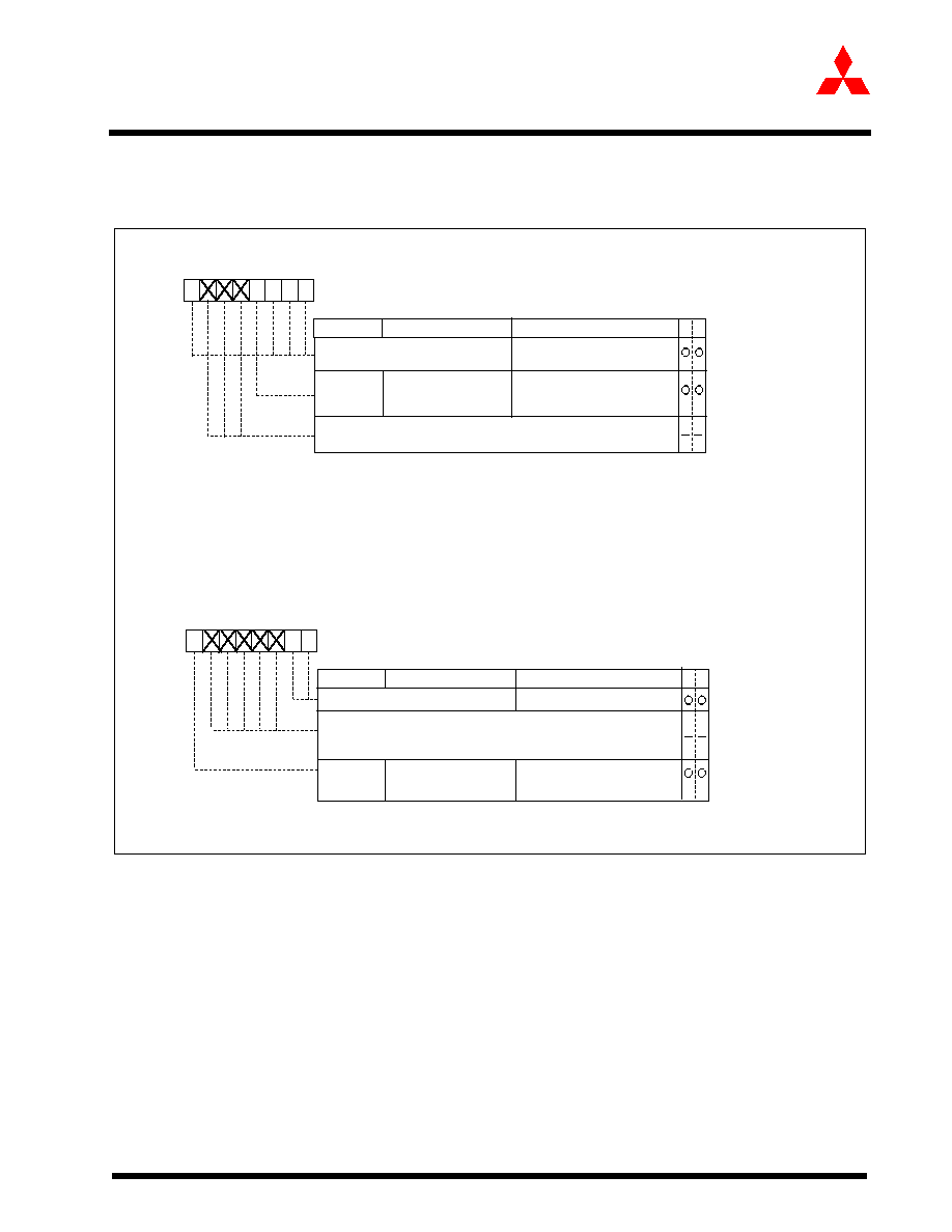
Figure 1.7 shows the processor mode registers 0 and 1.
Figure 1.7:
Processor mode registers 0 and 1
Processor mode register 0 (Note 1)
Symbol
Address
When reset
PM0
0004
16
00
16
(Note)
Bit name
Function
Bit symbol
W
R
b7
b6
b5
b4
b3
b2
b1
b0
Reserved bit
Note : Set bit 1 of the protect register (address 000A
16
) to "1" when writing new
values to this register.
Processor mode register 1 (Note)
Symbol
Address
When reset
PM1
0005
16
00XXXXX0
2
Bit name
Function
Bit symbol
W
R
b7
b6
b5
b4
b3
b2
b1
b0
Nothing is assigned.
These bits can neither be set nor reset. When read, their contents are
indeterminate.
Reserved bit
Must always be set to "0"
0
Note : Set bit 1 of the protect register (address 000A
16
) to "1" when writing new values
to this register.
PM17
Wait bit
0 : No wait state
1 : Wait state inserted
0
Must always be set to "0"
PM03
Software reset bit
The device is reset when this bit is set
to "1". The value of this bit is "0" when
read.
Nothing is assigned. These bits can neither be set nor reset. When read,
their contents are indeterminate.
0
0
0
0
0
0
1-15
Mitsubishi microcomputers
M30240 Group
SINGLE-CHIP 16-BIT CMOS MICROCOMPUTER
Preliminary Specifications REV. E
Specifications in this manual are tentative and subject to change
Memory
2.3 Memory
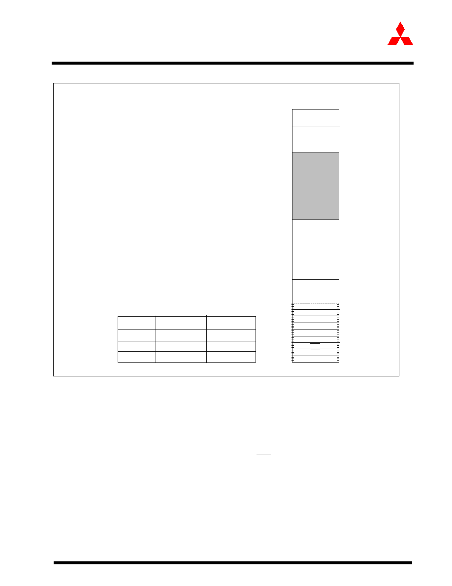
Figure 1.8:
Memory Map
Figure 1.8 is a memory map of the M30240 group. The address space extends the 1M bytes from
address 00000
16
to FFFFF
16
. Addresses above yyyyy
16
are ROM. For example, in the M30240ECFP,
there is 128K bytes of internal ROM from E0000
16
to FFFFF
16
. The special page vector table is mapped
from FFE00
16
to FFFDB
16
. If the starting addresses of subroutines or the destination addresses of jumps
are stored here, subroutine call instructions and jump instructions can be used as two-byte instructions,
reducing the number of program steps.
The vector table for fixed interrupts such as the reset and NMI are mapped from FFFDC
16
to FFFFF
16
.
The starting addresses of the interrupt routines are stored here. The address of the vector table for
software interrupts can be set as desired using the internal register (INTB). See Section 2.12 on
interrupts for further details.
Addresses below xxxxx
16
are RAM. For example, in M30240ECFP, 5K bytes of internal RAM are
mapped to the space from 00400
16
to 017FF
16
. In addition to storing data, the RAM also stores the stack
used when calling subroutines and when interrupts are generated.The SFR area is mapped to 00000
16
to 003FF
16
. This area accommodates control registers for peripheral devices such as I/O ports, A-D
converter, serial I/O, and timers. Section 2.4 describes the SFR area for peripheral unit control registers.
Any part of the SFR area that is unoccupied is reserved and cannot be used for other purposes.
yyyyy
16
Overflow
BRK instruction
Address match
Single step
Watchdog timer
Reset
00000
16
00400
16
XXXXX
16
ROM
unused
SFR
RAM
FFE00
16
FFFDC
16
FFFFF
16
Undefined instruction
Special page
vector table
DBC
NMI
Type
Address xxxxx
16
Address yyyyy
16
M30240M5
01000
16
F6000
16
M30240M6
01000
16
F4000
16
M30240ECFP 01800
16
E0000
16
1-16
Mitsubishi microcomputers
M30240 Group
SINGLE-CHIP 16-BIT CMOS MICROCOMPUTER
Preliminary Specifications REV. E
Specifications in this manual are tentative and subject to change
SFR MAP
2.4 SFR MAP
The table below shows the peripheral control registers, their addresses, names, acronyms, and values
after reset.
Address
Register name
Acronym
Value after reset
0000
16
0001
16
0002
16
0003
16
0004
16
Processor mode register 0
PM0
00
16
0005
16
Processor mode register 1
PM1
0 0
0
0006
16
System clock control register 0
CM0
48
16
0007
16
System clock control register 1
CM1
20
16
0008
16
0009
16
Address match interrupt enable register
AIER
0 0
000A
16
Protect register
PRCR
0 0 0
000B
16
000C
16
USB control register
USBC
00
16
000D
16
000E
16
Watchdog timer start register
WDTS
000F
16
Watchdog timer control register
WDC
0 0 0 ? ? ? ? ?
0010
16
Address match interrupt register 0
RMAD0
00
16
0011
16
00
16
0012
16
0 0 0 0
0013
16
0014
16
Address match interrupt register 1
RMAD1
00
16
0015
16
00
16
0016
16
0 0 0 0
0017
16
0018
16
0019
16
001A
16
001B
16
001C
16
001D
16
001E
16
Reserved
001F
16
USB attach / detach register
USBAD
00
16
0020
16
DMA0 source pointer
SAR0
0021
16
0022
16
0023
16
0024
16
DMA0 destination pointer
DAR0
0025
16
0026
16
0027
16
0028
16
DMA0 transfer counter
TCR0
0029
16
002A
16
002B
16
002C
16
DMA0 control register
DM0CON
0 0 0 0 0 ? 0 0
002D
16
002E
16
002F
16
0030
16
DMA1 source pointer
SAR1
0031
16
0032
16
0033
16
0034
16
DMA1 destination pointer
DAR1
0035
16
0036
16
0037
16
0038
16
DMA1 transfer counter
TCR1
0039
16
003A
16
003B
16
003C
16
DMA1 control register
DM1CON
0 0 0 0 0 ? 0 0
003D
16
003E
16
003F
16
1-17
Mitsubishi microcomputers
M30240 Group
SINGLE-CHIP 16-BIT CMOS MICROCOMPUTER
Preliminary Specifications REV. E
Specifications in this manual are tentative and subject to change
SFR MAP
0040
16
0041
16
0042
16
0043
16
0044
16
Suspend interrupt control register
SUSPIC
? 0 0 0
0045
16
0046
16
Resume interrupt control register
RSMIC
? 0 0 0
0047
16
USB SOF interrupt control register
SOFIC
0 0 ? 0 0 0
0048
16
0049
16
004A
16
Bus collision detection interrupt control register
BCNIC
? 0 0 0
004B
16
DMA0 interrupt control register
DM0IC
? 0 0 0
004C
16
DMA1 interrupt control register
DM1IC
? 0 0 0
004D
16
Key input interrupt control register
KUPIC
? 0 0 0
004E
16
A-D conversion interrupt control register
ADIC
? 0 0 0
004F
16
UART2 transmit interrupt control register
S2TIC
? 0 0 0
0050
16
UART2 receive interrupt control register
S2RIC
? 0 0 0
0051
16
UART0 transmit interrupt control register
S0TIC
? 0 0 0
0052
16
UART0 receive interrupt control register
S0RIC
? 0 0 0
0053
16
UART1 transmit interrupt control register
S1TIC
? 0 0 0
0054
16
UART1 receive interrupt control register
S1RIC
? 0 0 0
0055
16
TIMER A0 interrupt control register
TA0IC
? 0 0 0
0056
16
TIMER A1 interrupt control register
TA1IC
? 0 0 0
0057
16
TIMER A2 interrupt control register
TA2IC
? 0 0 0
0058
16
TIMER A3 interrupt control register
TA3IC
? 0 0 0
0059
16
TIMER A4 interrupt control register
TA4IC
? 0 0 0
005A
16
TIMER B0 interrupt control register
TB0IC
? 0 0 0
005B
16
TIMER B1 interrupt control register
TB1IC
? 0 0 0
005C
16
Reset interrupt control register
RSTIC
? 0 0 0
005D
16
INT0 interrupt control register
INT0IC
0 0 ? 0 0 0
005E
16
INT1 interrupt control register
INT1IC
0 0 ? 0 0 0
005F
16
USB function interrupt control register
USBFIC
? 0 0 0
- - -
0300
16
USB address register
USBA
00
16
0301
16
USB power management register
USBPM
00
16
0302
16
USB interrupt status register 1
USBIS1
00
16
0303
16
USB interrupt status register 2
USBIS2
00
16
0304
16
USB interrupt enable register 1
USBIE1
FF
16
0305
16
USB interrupt enable register 2
USBIE2
33
16
0306
16
USB frame number register low
USBSOFL
00
16
0307
16
USB frame number register high
USBSOFH
00
16
0308
16
USB ISO control register
USBISOC
00
16
0309
16
USB DMA0 source register
USBSAR0
00
16
030A
16
USB DMA1 source register
USBSAR1
00
16
030B
16
USB endpoint enable
USBEPEN
FF
16
030C
16
030D
16
030E
16
030F
16
0310
16
USB reserved
0311
16
USB EP 0 control/status register
EP0CS
00
16
0312
16
USB reserved
0313
16
USB EP 0 max packet size register
EP0MP
08
16
0314
16
USB reserved
0315
16
USB EP 0 OUT write count
EP0WC
00
16
0316
16
USB reserved
0317
16
USB reserved
0318
16
USB reserved
0319
16
USB EP 1 IN control/status register
EP1ICS
00
16
031A
16
USB EP 1 OUT control/status register
EP1OCS
00
16
031B
16
USB EP 1 IN max packet size register
EP1IMP
00
16
031C
16
USB EP 1 OUT max packet size register
EP1OMP
00
16
031D
16
USB EP 1 OUT write count
EP1WC
00
16
031E
16
USB reserved
031F
16
USB reserved
Address
Register name
Acronym
Value after reset

1-18
Mitsubishi microcomputers
M30240 Group
SINGLE-CHIP 16-BIT CMOS MICROCOMPUTER
Preliminary Specifications REV. E
Specifications in this manual are tentative and subject to change
SFR MAP
0320
16
USB reserved
0321
16
USB EP 2 IN control/status register
EP2ICS
00
16
0322
16
USB EP 2 OUT control/status register
EP2OCS
00
16
0323
16
USB EP 2 IN max packet size register
EP2IMP
00
16
0324
16
USB EP 2 OUT max packet size register
EP2OMP
00
16
0325
16
USB EP 2 OUT write count
EP2WC
00
16
0326
16
USB reserved
0327
16
USB reserved
0328
16
USB reserved
0329
16
USB EP 3 IN control/status register
EP3ICS
00
16
032A
16
USB EP 3 OUT control/status register
EP3OCS
00
16
032B
16
USB EP 3 IN max packet size register
EP3IMP
00
16
032C
16
USB EP 3 OUT max packet size register
EP3OMP
00
16
032D
16
USB EP 3 OUT write count
EP3WC
00
16
032E
16
USB reserved
00
16
032F
16
USB reserved
0330
16
USB reserved
0331
16
USB EP 4 IN control/status register
EP4ICS
00
16
0332
16
USB EP 4 OUT control/status register
EP4OCS
00
16
0333
16
USB EP 4 IN max packet size register
EP4IMP
00
16
0334
16
USB EP 4 OUT max packet size register
EP4OMP
00
16
0335
16
USB EP 4 OUT write count
EP4WC
00
16
0336
16
USB reserved
0337
16
USB reserved
0338
16
USB EP 0 FIFO
EP0
0339
16
USB EP 1 FIFO
EP1
033A
16
USB EP 2 FIFO
EP2
033B
16
USB EP 3 FIFO
EP3
033C
16
USB EP 4 FIFO
EP4
033D
16
reserved
033E
16
reserved
033F
16
reserved
0340
16
0341
16
0342
16
0343
16
0344
16
0345
16
0346
16
0347
16
0348
16
0349
16
034A
16
034B
16
034C
16
034D
16
034E
16
034F
16
0350
16
0351
16
0352
16
0353
16
0354
16
0355
16
0356
16
0357
16
0358
16
0359
16
035A
16
035B
16
035C
16
035D
16
035E
16
035F
16
Address
Register name
Acronym
Value after reset
1-19
Mitsubishi microcomputers
M30240 Group
SINGLE-CHIP 16-BIT CMOS MICROCOMPUTER
Preliminary Specifications REV. E
Specifications in this manual are tentative and subject to change
SFR MAP
0370
16
0371
16
0372
16
0373
16
0374
16
0375
16
0376
16
0377
16
Reserved
0378
16
UART2 transmit / receive mode register
U2MR
00
16
0379
16
UART2 bit rate generator
U2BRG
037A
16
UART2 transmit buffer register
U2TB
037B
16
037C
16
UART2 transmit /receive control register 0
U2C0
08
16
037D
16
UART2 transmit / receive control register 1
U2C1
02
16
037E
16
UART2 receive buffer register
U2RB
037F
16
0380
16
Count start flag
TABSR
00
16
0381
16
Reserved
0382
16
One-shot start flag
ONSF
0 0
0 0 0 0 0
0383
16
Trigger select register
TRGSR
00
16
0384
16
Up-down flag
UDF
00
16
0385
16
0386
16
Timer A0
TA0
0387
16
0388
16
Timer A1
TA1
0389
16
038A
16
Timer A2
TA2
038B
16
038C
16
Timer A3
TA3
038D
16
038E
16
Timer A4
TA4
038F
16
0390
16
Timer B0
TB0
0391
16
0392
16
Timer B1
TB1
0393
16
0394
16
Timer B2
TB2
0395
16
0396
16
Timer A0 mode register
TA0MR
00
16
0397
16
Timer A1 mode register
TA1MR
00
16
0398
16
Timer A2 mode register
TA2MR
00
16
0399
16
Timer A3 mode register
TA3MR
00
16
039A
16
Timer A4 mode register
TA4MR
00
16
039B
16
Timer B0 mode register
TB0MR
0 0 ?
0 0 0 0
039C
16
Timer B1 mode register
TB1MR
0 0 ?
0 0 0 0
039D
16
Timer B2 mode register
TB2MR
0 0 ?
0 0 0 0
039E
16
039F
16
03A0
16
UART0 transmit / receive mode register
U0MR
00
16
03A1
16
UART0 bit rate generator
U0BRG
03A2
16
UART0 transmit buffer register
U0TB
03A3
16
03A4
16
UART0 transmit / receive control register 0
U0C0
08
16
03A5
16
UART0 transmit / receive control register 1
U0C1
02
16
03A6
16
UART0 receive buffer register
U0RB
03A7
16
03A8
16
UART1 transmit / receive mode register
U1MR
00
16
03A9
16
UART1 bit rate generator
U1BRG
03AA
16
UART1 transmit buffer register
U1TB
03AB
16
03AC
16
UART1 transmit / receive control register 0
U1C0
08
16
03AD
16
UART1 transmit / receive control register 1
U1C1
02
16
03AE
16
UART1 receive buffer register
U1RB
03AF
16
Address
Register name
Acronym
Value after reset
1-20
Mitsubishi microcomputers
M30240 Group
SINGLE-CHIP 16-BIT CMOS MICROCOMPUTER
Preliminary Specifications REV. E
Specifications in this manual are tentative and subject to change
SFR MAP
03B0
16
UART transmit / receive control register 2
UCON
0 0 0 0 0 0 0
03B1
16
03B2
16
03B3
16
03B4
16
03B5
16
03B6
16
03B7
16
03B8
16
DMA0 cause select register
DM0SL
00
16
03B9
16
03BA
16
DMA1 cause select register
DM1SL
00
16
03BB
16
03BC
16
CRC data register
CRCD
03BD
16
03BE
16
CRC input register
CRCIN
03BF
16
03C0
16
A-D register 0
AD0
03C1
16
03C2
16
A-D register 1
AD1
03C3
16
03C4
16
A-D register 2
AD2
03C5
16
03C6
16
A-D register 3
AD3
03C7
16
03C8
16
A-D register 4
AD4
03C9
16
03CA
16
A-D register 5
AD5
03CB
16
03CC
16
A-D register 6
AD6
03CD
16
03CE
16
A-D register 7
AD7
03CF
16
03D0
16
03D1
16
03D2
16
03D3
16
03D4
16
A-D control register 2
ADCON2
0
03D5
16
03D6
16
A-D control register 0
ADCON0
0 0 0 0 0 ? ? ?
03D7
16
A-D control register 1
ADCON1
00
16
03D8
16
03D9
16
03DA
16
03DB
16
Frequency synthesizer clock control
FSCCR
00
16
03DC
16
Frequency synthesizer control
FSC
60
16
03DD
16
Frequency synthesizer multiplier control
FSM
FF
16
03DE
16
Frequency synthesizer prescaler control
FSP
FF
16
03DF
16
Frequency synthesizer divider
FSD
FF
16
03E0
16
Port P0
P0
03E1
16
Port P1
P1
03E2
16
Port P0 direction register
PD0
00
16
03E3
16
Port P1 direction register
PD1
00
16
03E4
16
Port P2
P2
03E5
16
Port P3
P3
03E6
16
Port P2 direction register
PD2
00
16
03E7
16
Port P3 direction register
PD3
00
16
03E8
16
03E9
16
03EA
16
03EB
16
03EC
16
Port P6
P6
03ED
16
Port P7
P7
03EE
16
Port P6 direction register
PD6
00
16
03EF
16
Port P7 direction register
PD7
00
16
Address
Register name
Acronym
Value after reset

1-21
Mitsubishi microcomputers
M30240 Group
SINGLE-CHIP 16-BIT CMOS MICROCOMPUTER
Preliminary Specifications REV. E
Specifications in this manual are tentative and subject to change
SFR MAP
03F0
16
Port P8
P8
03F1
16
03F2
16
Port P8 direction register
PD8
0 0
0 0 0 0 0
03F3
16
03F4
16
Port P10
P10
03F5
16
03F6
16
Port P10 direction register
PD10
00
16
03F7
16
03F8
16
03F9
16
03FA
16
P2 drive capacity
P2DR
00
16
03FB
16
Timer A Output Drive Capacity
TADR
00
16
03FC
16
Pull-up control register 0
PUR0
00
16
03FD
16
Pull-up control register 1
PUR1
00
16
03FE
16
03FF
16
Address
Register name
Acronym
Value after reset
1-22
Mitsubishi microcomputers
M30240 Group
SINGLE-CHIP 16-BIT CMOS MICROCOMPUTER
Preliminary Specifications REV. E
Specifications in this manual are tentative and subject to change
Reset
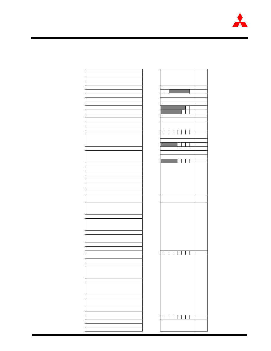
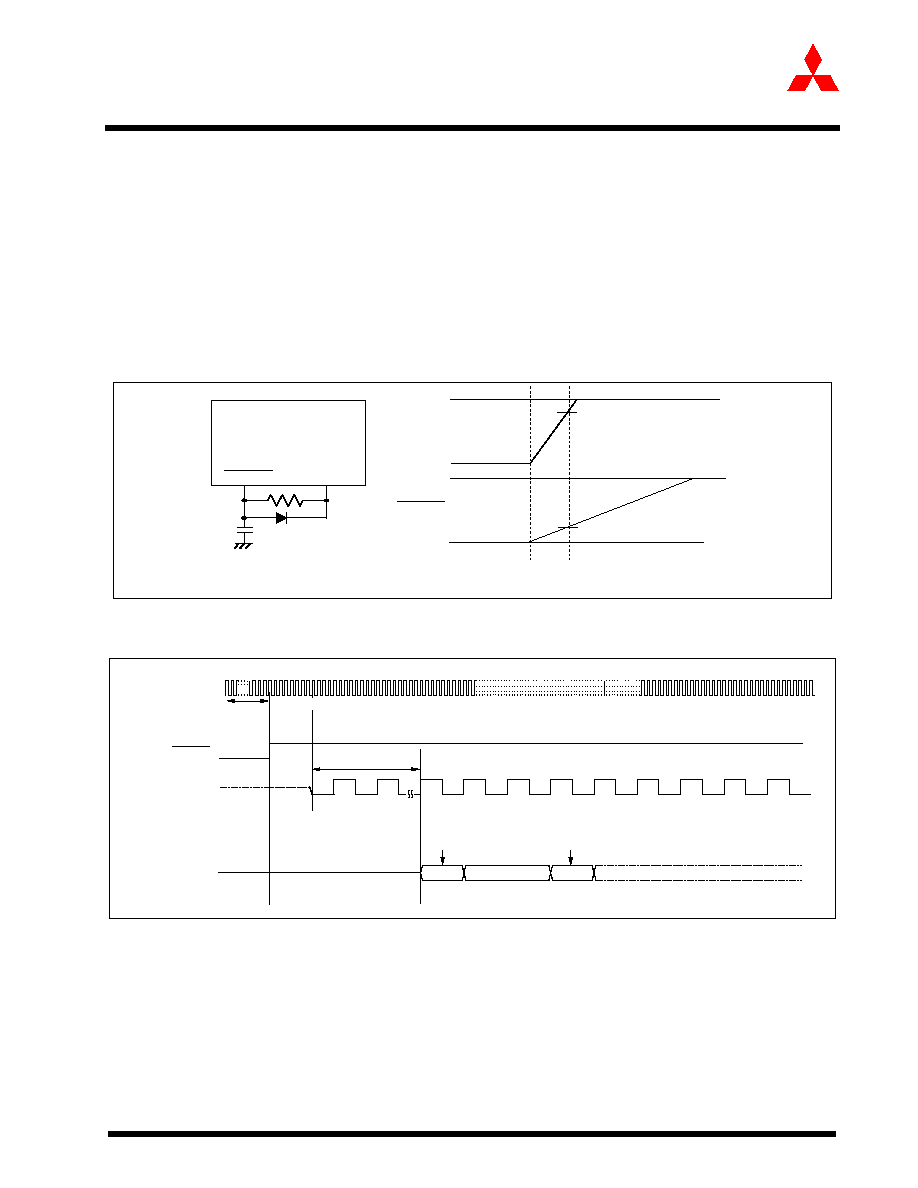
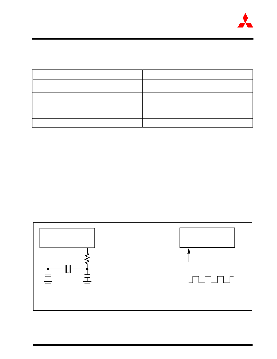
2.5 Reset
There are two types of resets: hardware and software. In both cases, operation is the same after the
reset. (See "Software Reset" for further details regarding software resets.) This section explains on
hardware resets.
When the supply voltage is within the range where operation is guaranteed, a reset is effected by holding
the reset pin level "L" (0.2VCC max.) for at least 20 f(X
IN
) cycles. When the reset pin level is then
returned to the "H" level while main clock is stable, the reset status is cancelled and program execution
resumes from the address in the reset vector table.
Figure 1.9 shows an example of a reset circuit. Figure 1.10 shows the reset sequence.
.
Figure 1.9:
Reset circuit
Figure 1.10: Reset sequence
RESET
V
CC
0.8V
RESET
V
CC
0V
0V
5V
5V
4.0V
Example when V
CC
= 5V
.
Address
Content of reset vector
Internal clock
F
24 cycles
FFFFE
16
X
IN
RESET
FFFFC
16
At least 20 cycles are needed
Internal clock
F
1-23
Mitsubishi microcomputers
M30240 Group
SINGLE-CHIP 16-BIT CMOS MICROCOMPUTER
Preliminary Specifications REV. E
Specifications in this manual are tentative and subject to change
Software Reset
When the RESET pin level = "L", all ports change to input mode (floating.) Table 1.4 shows the status
of the other pins while the RESET pin level is "L".
Table 1.4:
Main clock-generating circuits
2.6 Software Reset
Writing a "1" to bit 3 of the processor mode register 0 (address 0004
16
) applies a (software) reset to the
microcomputer. A software reset has almost the same effect as a hardware reset with the following
exceptions:
� The contents of internal RAM are preserved
� All USB, DC-DC converter, and PLL SFR values are preserved. (See Section 2.4)
2.7 Clock-Generating Circuit
The clock-generating circuit contains one oscillator circuit that supplies the operating clock sources to
the CPU and internal peripheral units.Example of oscillator circuit
Figure 1.11 shows some examples of the main clock circuit, one using an oscillator connected to the
circuit, and the other one using an externally derived clock for input. Circuit constants in Figure 1.11 vary
with each oscillator used. Use circuit constant values recommended by the oscillator manufacturer.
Figure 1.11: Examples of clock source
Functions
Main clock-generating circuit
Use of clock
� CPU's operating clock source
� Internal peripheral units' operating clock source
Usable oscillator
Ceramic or crystal oscillator
Pins to connect oscillator
Xin
, Xout
Oscillation stop/restart function
Available
Oscillator status immediately after reset
Oscillating
Microcomputer
(Built-in feedback resistor)
X
IN
X
OUT
Externally derived clock
Open
Vcc
Vss
Microcomputer
(Built-in feedback resistor)
X
IN
X
OUT
R
d
C
IN
C
OUT
(Note)
Note: Insert a damping resistor if required. The resistance will vary depending on the oscillator and the oscillation drive
capacity setting. Use the value recommended by the maker of the oscillator.
When the oscillation drive capacity is set to low, check that oscillation is stable.
1-24
Mitsubishi microcomputers
M30240 Group
SINGLE-CHIP 16-BIT CMOS MICROCOMPUTER
Preliminary Specifications REV. E
Specifications in this manual are tentative and subject to change
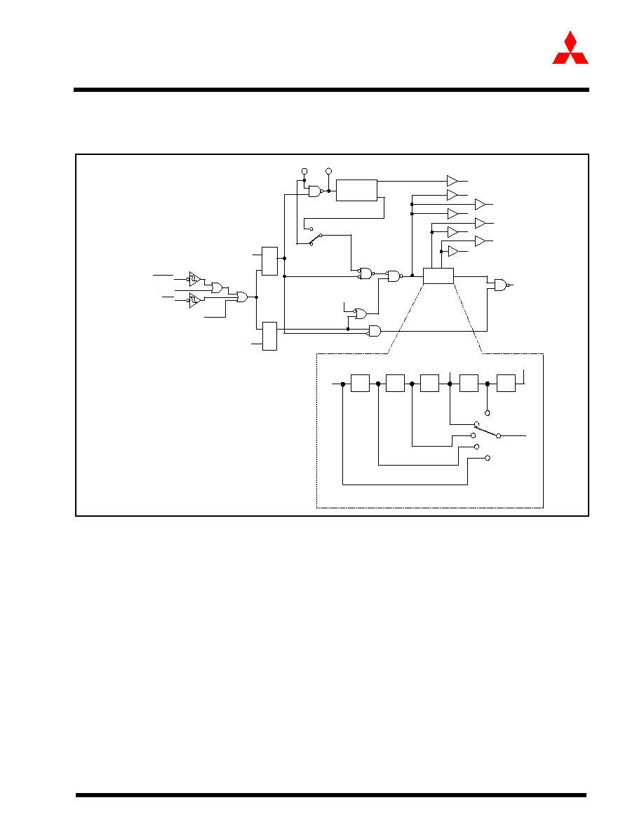
Clock Control
2.8 Clock Control
Figure 1.12 shows the block diagram of the clock-generating circuit.
Figure 1.12: Clock-generating circuit
The following paragraphs describe the clocks generated by the clock-generating circuit.
2.8.1 Main clock
The main clock is generated by the main clock oscillation circuit. After a reset, the clock is divided by
8 to the internal clock
. The clock can be stopped using the main clock stop bit (bit 5 at address
0006
16
). Stopping the clock reduces the power dissipation.
After the oscillation of the main clock oscillation circuit has stabilized, the drive capacity of the f(Xout)
pin can be reduced using the f(Xin)-f(Xout) drive capacity select bit (bit 5 at address 0007
16
). Reducing
the drive capacity of the f(Xout) pin reduces the power dissipation. This bit defaults to "1" when shifting
to stop mode and after a reset.
2.8.2 Internal clock
The internal clock
is the clock that drives the CPU, and is either the main clock or is derived by di-
viding the main clock by 2, 4, 8, or 16. The internal clock
is derived by dividing the main clock by 8
after a reset.
When shifting to stop mode, the main clock division select bit (bit 6 at 0006
16
) is set to "1".
CM0i : Bit i at address 0006
16
CM1i : Bit i at address 0007
16
FSCCRi: Bit i at address 03DB
16
WAIT instruction
CM02
Q
S
R
NMI
Interrupt request
level judgment
output
RESET
Software reset
f
AD
Divider
a
d
1/2
1/2
1/2
1/2
CM06=0
CM17,CM16=00
CM06=0
CM17,CM16=01
CM06=0
CM17,CM16=10
CM06=1
CM06=0
CM17,CM16=11
d
a
Details of divider
c
b
b
1/2
c
f
1
f
32
SIO2
f
8
SIO2
f
1
SIO2
f
8
f
32
X
OUT
Main clock
CM10 "1"
Write signal
Q
S
R
X
IN
Frequency
Synthesizer
Circuit
f
usb (48MHz)
FSCCR0=1
FSCCR0=0
Internal clock
fsyn
1-25
Mitsubishi microcomputers
M30240 Group
SINGLE-CHIP 16-BIT CMOS MICROCOMPUTER
Preliminary Specifications REV. E
Specifications in this manual are tentative and subject to change
Clock Control
2.8.3 Peripheral function clock
2.8.3.1 � f1, f8, f32
The clock for the peripheral devices is derived from the main clock or by dividing it by 8 or 32. The
peripheral function clock is stopped by stopping the main clock or by setting the WAIT peripheral func-
tion clock stop bit (bit 2 at 0006
16
) to "1" and then executing a WAIT instruction.
2.8.3.2 � fAD
This clock has the same frequency as the main clock and is used for A-D conversion.
2.8.4 Clock Output
In single-chip mode, the clock output function select bits (bits 0 and 1 at address 0006
16
) enable f8 or
f32 to be output from the P37/CLKOUT pin. When the WAIT peripheral function clock stop bit (bit 2 at
address 0006
16
) is set to "1", the output of f8 and f32 stops when a WAIT instruction is executed.
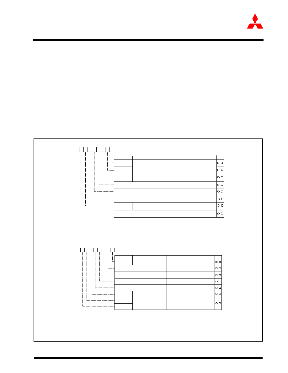
Figure 1.13 shows the system clock control registers 0 and 1.
Figure 1.13: System clock control registers 0 and 1
Note 1: Set bit 0 of the protect register (address 000A
16
) to "1"
before writing to this register.
Note 2: Changes to "1" when shifting to stop mode.
Note 3: Can be selected when bit 6 of system clock control
register 0 (address 0006
16
) is "0". If "1", division mode if fixed at 8.
System clock control register 0 (Note 1)
Note 1: Set bit 0 of the protect register (address 000A
16
) to "1" before writing
to this register.
Note 2: Changes to "1" when shifting to stop mode.
System clock control register 1 (Note 1)
Symbol
Address
When reset
CM1
0007
16
20
16
Bit name
Function
Bit symbol
b7
b6
b5
b4
b3
b2
b1
b0
CM10
All clock stop control bit
0 : Clock on
1 : All clocks off (stop mode)
CM15
X
IN
-X
OUT
drive capacity
select bit (Note 2)
0 : LOW
1 : HIGH
W
R
CM16
CM17
Reserved bit
Always set to
"0"
Reserved bit
Always set to
"0"
Main clock division select
bit 1 (Note 3)
0 0 : No division mode
0 1 : Division by 2 mode
1 0 : Division by 4 mode
1 1 : Division by 16 mode
b7 b6
0
0
Reserved bit
Always set to
"0"
Reserved bit
Always set to
"0"
0
0
Symbol
Address
When reset
CM0
0006
16
48
16
Bit name
Function
Bit symbol
b7
b6
b5
b4
b3
b2
b1
b0
0 0 : I/O port P3
7
0 1 : Invalid
1 0 : f
8
output
1 1 : f
32
output
b1 b0
CM01
CM02
CM00
Clock output function
select bit
WAIT peripheral function
clock stop bit
0 : Do not stop f
1
, f
8
, f
32
in wait mode
1 : Stop f
1
, f
8
, f
32
in wait mode
W
R
CM06
Main clock division select
bit 0 (Note 2)
0 : CM16 and CM17 valid
1 : Division by 8 mode
Reserved bit
Always set to "1"
Reserved bit
Always set to "0"
Reserved bit
Always set to "0"
Reserved bit
Always set to "0"

1-26
Mitsubishi microcomputers
M30240 Group
SINGLE-CHIP 16-BIT CMOS MICROCOMPUTER
Preliminary Specifications REV. E
Specifications in this manual are tentative and subject to change
Stop Mode
2.9 Stop Mode
Writing "1" to the all-clock stop control bit (bit 0 at address 0007
16
) stops all oscillation and the
microcomputer enters stop mode. In stop mode, the content of the internal RAM is retained provided
that VCC remains above 2V.
Because the oscillation of internal clock
, f1 to f32, and fAD stops in stop mode, peripheral functions
such as the A-D converter and watchdog timer do not function. However, timer A operates, provided that
the event counter mode is set to an external pulse, and UARTi (i = 0 to 2) functions provided an external
clock is selected. Table 1.5 shows the status of the ports in stop mode.
Stop mode is cancelled by a hardware reset or interrupt. If an interrupt is to be used to cancel stop mode,
that interrupt must first have been enabled. The I flag must also be set prior to stopping for an interrupt
to cancel it. After coming out of stop mode, it is recommended that five "NOP" instructions be executed
to clear the instruction queue.
When shifting to stop mode, the main clock division select bit 0 (bit 6 at 0006
16
) is set to "1".
Table 1.5:
Port status during stop mode
2.10 Wait Mode
When a WAIT instruction is executed, the internal clock
stops and the microcomputer enters the wait
mode. In this mode, oscillation continues but the internal clock
and watchdog timer stop. Writing "1"
to the WAIT peripheral function clock stop bit and executing a WAIT instruction stops the clock being
supplied to the internal peripheral functions, allowing power dissipation to be reduced. Table 1.6 shows
the status of the ports in wait mode.
Wait mode is cancelled by a hardware reset or interrupt. If an interrupt is used to cancel wait mode, the
microcomputer restarts using as internal clock
the clock that had been selected when the WAIT
instruction was executed
Table 1.6:
Port status during wait mode
2.11 Status Transition Of the Internal Clock
Power dissipation can be reduced and low-voltage operation achieved by changing the count source for
internal clock
. Table 1.7 shows the operating modes corresponding to the settings of system clock
control registers 0 and 1.
After a reset, operation defaults to division by 8 mode. When shifting to stop mode, the main clock
division select bit 0 (bit 6 at address 0006
16
) is set to "1". The following shows the operational modes of
internal clock
2.11.1 Division by 2 mode
The main clock is divided by 2 to obtain the internal clock
.
Pin
Single-chip mode
Port
Retains status before stop mode
CLKOUT
Retains status before stop mode
Pin
Single-chip mode
Port
Retains status before stop mode
CLKout
Does not stop when the WAIT peripheral function clock stop bit is "0"
When the WAIT peripheral function clock stop bit is "1", the status immediately
prior to entering wait mode is maintained.

1-27
Mitsubishi microcomputers
M30240 Group
SINGLE-CHIP 16-BIT CMOS MICROCOMPUTER
Preliminary Specifications REV. E
Specifications in this manual are tentative and subject to change
Power Control
2.11.2 Division by 4 mode
The main clock is divided by 4 to obtain the internal clock
.
2.11.3 Division by 8 mode
The main clock is divided by 8 to obtain the internal clock
. Note that oscillation of the main clock
must have stabilized before transferring from this mode to another mode.
2.11.4 Division by 16 mode
The main clock is divided by 16 to obtain the internal clock
.
2.11.5 No-division mode
The main clock is used as internal clock.
Table 1.7:
Operating modes dictated by settings of system clock control registers 0 and 1
2.12 Power Control
The following is a description of the three available power control modes:
2.12.0.1 Normal Operation Mode
�
High-speed mode
Divide-by-1 frequency of the main clock become the internal clock
. The CPU operates with the internal clock
selected. Each peripheral function operates according to its assigned clock.
�
Medium-speed mode
Divide-by-2, divide-by-4, divide-by-8, or divide-by-16 frequency of the main clock becomes the internal clock
. The CPU operates according to the internal clock selected. Each peripheral function operates according
to its assigned clock.
2.12.0.2 Wait mode
The CPU operation is stopped. The oscillators do not stop.
2.12.0.3 Stop Mode
All oscillators stop. The CPU and all built-in peripheral functions stop. Of the three modes listed, this mode is
the most effective in decreasing power consumption.
CM17
CM16
CM06
Operating mode of internal clock
0
1
0
Division by 2 mode
1
0
0
Division by 4 mode
Invalid
Invalid
1
Division by 8 mode
1
1
0
Division by 16 mode
0
0
0
No-division mode
1-28
Mitsubishi microcomputers
M30240 Group
SINGLE-CHIP 16-BIT CMOS MICROCOMPUTER
Preliminary Specifications REV. E
Specifications in this manual are tentative and subject to change
Protection
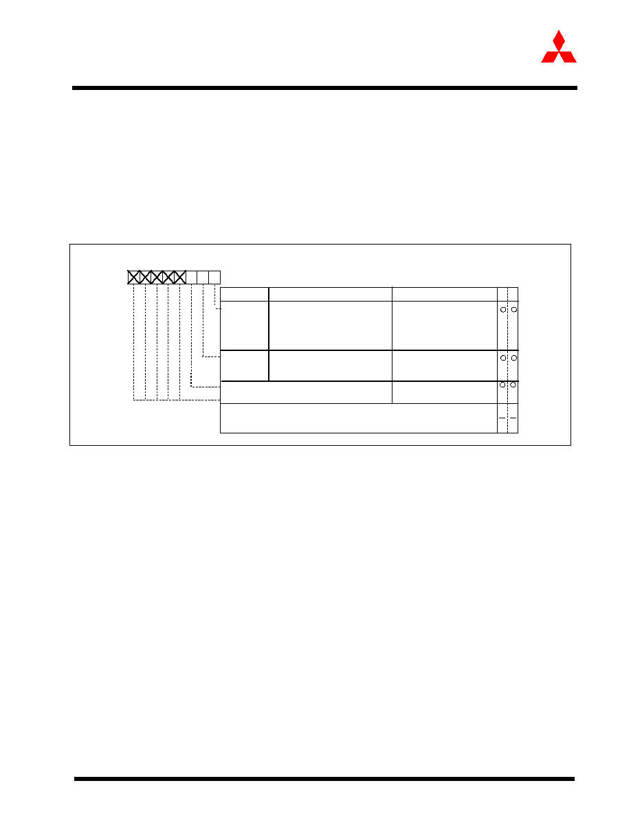
2.13 Protection
The protection function is provided so that the values in important registers cannot be changed in the
event that the program runs out of control. Figure 1.14 shows the protect register. The values in the
processor mode register 0 (address 0004
16
), processor mode register 1 (address 0005
16
), system clock
control register 0 (address 0006
16
), system clock control register 1 (address 0007
16
) and frequency
synthesizer registers can only be changed when the respective bit in the protect register is set to "1".
The system clock control registers 0 and 1 write-enable bit (bit 0 at 000A
16
) and processor mode register
0 and 1 write-enable bit (bit 1 at 000A
16
) do not automatically return to "0" after a value has been written
to an address. The program must therefore be written to return these bits to "0".
Figure 1.14: Protect register
Protect register
Symbol
Address
When reset
PRCR
000A
16
XXXXX000
2
Bit name
Bit symbol
b7
b6
b5
b4
b3
b2
b1
b0
0 : Write-inhibited
1 : Write-enabled
PRC1
PRC0
Enables writing to processor mode
registers 0 and 1 (addresses 0004
16
and 0005
16
)
Function
0 : Write-inhibited
1 : Write-enabled
Enables writing to system clock
control registers 0 and 1 (addresses
0006
16
and 0007
16
) and frequency
synthesizer registers (addresses
03DB
16
to 03DF
16
)
W
R
Nothing is assigned.
These bits can neither be set nor reset. When read, their contents are
indeterminate.
Reserved bit
Must always be set to "0"
1-29
Mitsubishi microcomputers
M30240 Group
SINGLE-CHIP 16-BIT CMOS MICROCOMPUTER
Preliminary Specifications REV. E
Specifications in this manual are tentative and subject to change
Interrupts
2.14 Interrupts
Table 1.8 and Table 1.9 show the interrupt sources and vector table addresses. When an interrupt is
received, the program is executed from the address shown by the respective interrupt vector.
The vector table addresses for the interrupts in Table 7 are fixed (interrupt vector addresses). These
interrupts are not affected by the interrupt enable flag (I flag) (non-maskable interrupts).
The vector table addresses for the interrupts in Table 8 are variable, being determined as relative to the
fixed address in the interrupt table register (INTB). These interrupts can be enabled or disabled using
the interrupt enable flag (I flag) (maskable interrupts). Sixty four vectors can be set in the interrupt table
register (INTB). Any of software interrupts 0 to 63 can be assigned to each vector. By using the INT
instruction to specify a software interrupt number, the program can be executed starting at the address
indicated by the respective vector. The BRK instruction interrupt has interrupt vectors in both the fixed
vector address and variable vector address. When the contents of FFFE4
16
through FFFE7
16
are all
"FF
16
), the program is executed from the address shown in the BRK instruction interrupt vector in the
variable vector address.
Specify the starting address of the interrupt program in the interrupt vector. Figure 1.15 shows the format
for specifying the address.
Note: Interrupts used for debugging purposes only
Figure 1.15: Format for specifying interrupt vector addresses
Table 1.8:
Interrupt vectors (fixed interrupt vector addresses)
Interrupt source
Vector table addresses
Address(L) to Address(H)
Remarks
Undefined instruction
FFFDC
16
to FFFDF
16
Interrupt on UND instruction
Overflow
FFFE0
16
to FFFE3
16
Interrupt on INTO instruction
BRK instruction
FFFE4
16
to FFFE7
16
If the vector is filled with FF
16
, program execution starts from
the address shown by the vector in the variable vector table
Address Match
FFFE8
16
to FFFEB
16
There is an address-matching interrupt enable bit
Single Step (Note)
FFFEC
16
to FFFEF
16
Do not use
Watchdog timer
FFFF0
16
to FFF3
16
DBC (Note)
FFFF4
16
to FFFF7
16
Do not use
NMI
FFFF8
16
to FFFFB
16
External interrupt by NMI pin
Reset
FFFFC
16
to FFFFF
16
Mid address
Low address
0 0 0 0
High address
0 0 0 0
0 0 0 0
Vector address + 0
Vector address + 1
Vector address + 2
Vector address + 3
LSB
MSB

1-30
Mitsubishi microcomputers
M30240 Group
SINGLE-CHIP 16-BIT CMOS MICROCOMPUTER
Preliminary Specifications REV. E
Specifications in this manual are tentative and subject to change
Interrupts
Table 1.9:
Interrupt vectors (variable interrupt vector addresses)
Note 1:Address relative to address in interrupt table base address register (INTB)
Software interrupt number
Vector table addresses
Address(L) to Address(H)
Interrupt source
Remarks
Software interrupt number 0
+0 to +3 (Note 1)
BRK instruction
Cannot be masked by I flag
Software interrupt number 4
+16 to +19
USB Suspend
Software interrupt number 6
+24 to +27
USB Resume
Software interrupt number 7
+28 to +31
USB Start of Frame
Software interrupt number 10
+40 to +43
Bus collision detection
Software interrupt number 11
+44 to +47
DMA0
Software interrupt number 12
+48 to +51
DMA1
Software interrupt number 13
+52 to +55
Key input interrupt
Software interrupt number 14
+56 to +59
A-D
Software interrupt number 15
+60 to +63
UART2 transmit
Software interrupt number 16
+64 to +67
UART2 receive
Software interrupt number 17
+68 to +71
UART0 transmit
Software interrupt number 18
+72 to +75
UART0 receive
Software interrupt number 19
+76 to +79
UART1 transmit
Software interrupt number 20
+80 to +83
UART1 receive
Software interrupt number 21
+84 to +87
Timer A0
Software interrupt number 22
+88 to +91
Timer A1
Software interrupt number 23
+92 to +95
Timer A2
Software interrupt number 24
+96 to +99
Timer A3
Software interrupt number 25
+100 to +103
Timer A4
Software interrupt number 26
+104 to +107
Timer B0
Software interrupt number 27
+108 to +111
Timer B1
Software interrupt number 28
+112 to +115
USB Reset
Software interrupt number 29
+116 to +119
INT0
Software interrupt number 30
+120 to +123
INT1
Software interrupt number 31
+124 to +127
USB Function
Software interrupt number 32
to
Software interrupt number 63
+252 to +255
Software interrupt
Cannot be masked by I flag

1-31
Mitsubishi microcomputers
M30240 Group
SINGLE-CHIP 16-BIT CMOS MICROCOMPUTER
Preliminary Specifications REV. E
Specifications in this manual are tentative and subject to change
Interrupts
2.14.1 Interrupt control registers
Peripheral I/O interrupts have their own interrupt control registers. Table 1.10 shows the addresses
of the interrupt control registers. Figure 1.16 shows the interrupt control registers.
The interrupt request bit is set by hardware to "0" when an interrupt request is received. The interrupt
request bit can also be set by software to "0". (Do not set to "1".)
INT0 and INT1 are triggered by the edges of external inputs. The edge polarity is selected using the
polarity select bit. (Other interrupts are described elsewhere.)
An interrupt must first be enabled before it can be used to cancel stop mode.
Table 1.10:
Addresses in interrupt control register
Interrupt control register
Symbol
name
Address
Interrupt control register
Symbol
name
Address
USB Suspend Interrupt
SUSPIC
0044
16
UART1 receive
S1RIC
0054
16
USB Resume interrupt
RSMIC
0046
16
Timer A0
TA0IC
0055
16
USB Start Of Frame
SOFIC
0047
16
Timer A1
TA1IC
0056
16
Bus collision detection
BCNIC
004A
16
Timer A2
TA2IC
0057
16
DMA0
DM0IC
004B
16
Timer A3
TA3IC
0058
16
DMA1
DM1IC
004C
16
Timer A4
TA4IC
0059
16
Key input interrupt
KUPIC
004D
16
Timer B0
TB0IC
005A
16
A-D
ADIC
004E
16
Timer B1
TB1IC
005B
16
UART2 transmit
S2TIC
004F
16
USB Reset
RSTIC
005C
16
UART2 receive
S2RIC
0050
16
INT0
INT0IC
005D
16
UART0 transmit
S0TIC
0051
16
INT1
INT1IC
005E
16
UART0 receive
S0RIC
0052
16
USB Function
USBFIC
005F
16
UART1 transmit
S1TIC
0053
16
1-32
Mitsubishi microcomputers
M30240 Group
SINGLE-CHIP 16-BIT CMOS MICROCOMPUTER
Preliminary Specifications REV. E
Specifications in this manual are tentative and subject to change
Interrupts
Figure 1.16: Interrupt control registers
Symbol
Address
When reset
INTiIC ( i= 0, 1)
005D
16,
005E
16
XX00X000
2
SOFIC
0047
16
XX00X000
2
Interrupt control register
Symbol
Address
When reset
SUSPIC
0044
16
XXXXX000
2
RSMIC
0046
16
XXXXX000
2
BCNIC
004A
16
XXXXX000
2
DMiIC(i=0, 1)
004B
16
, 004C
16
XXXXX000
2
KUPIC
004D
16
XXXXX000
2
ADIC
004E
16
XXXXX000
2
SiTIC(i=0 to 2)
0051
16
, 0053
16
, 004F
16
XXXXX000
2
SiRIC(i=0 to 2)
0052
16
, 0054
16
, 0050
16
XXXXX000
2
TAiIC(i=0 to 4)
0055
16
to 0059
16
XXXXX000
2
TBiIC(i=0 to 2)
005A
16
to 005B
16
XXXXX000
2
RSTIC
005C
16
XXXXX000
2
USBFIC
005F
16
XXXXX000
2
b7
b6
b5
b4
b3
b2
b1
b0
Bit name
Function
Bit symbol
W
R
ILVL0
IR
Interrupt priority level
select bit
Interrupt request bit
0 : Interrupt not requested
1 : Interrupt requested
ILVL1
ILVL2
Nothing is assigned.
These bits can neither be set nor reset. When read, their contents are
indeterminate.
(Note)
Note: This bit can only be reset (= 0), but cannot be set ( = 1).
0 0 0 : Level 0 (interrupt disabled)
0 0 1 : Level 1
0 1 0 : Level 2
0 1 1 : Level 3
1 0 0 : Level 4
1 0 1 : Level 5
1 1 0 : Level 6
1 1 1 : Level 7
b2 b1 b0
Bit name
Function
Bit symbol
W
R
b7
b6
b5
b4
b3
b2
b1
b0
ILVL0
IR
POL
Nothing is assigned.
These bits can neither be set nor reset. When read, their contents are
indeterminate.
Interrupt priority level
select bit
Interrupt request bit
Polarity select bit
Reserved bit
0: Interrupt not requested
1: Interrupt requested
0 : Selects falling edge
1 : Selects rising edge
Always set to "0"
ILVL1
ILVL2
(Note 1)
0 0 0 : Level 0 (interrupt disabled)
0 0 1 : Level 1
0 1 0 : Level 2
0 1 1 : Level 3
1 0 0 : Level 4
1 0 1 : Level 5
1 1 0 : Level 6
1 1 1 : Level 7
b2 b1 b0
0
(Note 2)
Note 1: This bit can only be reset (=0), but cannot be set (=1).
Note 2: For SOFIC (address 0047
1 6
), a "0" should always be written.

1-33
Mitsubishi microcomputers
M30240 Group
SINGLE-CHIP 16-BIT CMOS MICROCOMPUTER
Preliminary Specifications REV. E
Specifications in this manual are tentative and subject to change
Interrupts
2.14.2 Interrupt priority
The order of priority when two or more interrupts are generated simultaneously is determined by both
hardware and software.
The interrupt priority levels determined by hardware are reset > NMI > DBC > watchdog timer > pe-
ripheral I/O interrupts > single-step > address matching interrupt.
The interrupt priority levels determined by software are set in the interrupt control registers.
Figure 1.17 shows the circuit that judges the interrupt hardware priority level. When two or more inter-
rupts are generated simultaneously, the interrupt with the higher software priority is selected. Howev-
er, if the interrupts have the same software priority level, the interrupt is selected according to the
hardware priority set in the circuit.
The selected interrupt is accepted only when the priority level is higher than the processor interrupt
priority level (IPL) in the flag register (FLG) and the interrupt enable flag (I flag) is "1". Note that the
reset, NMI, DBC, watchdog timer, single-step, address-match, BRK instruction, overflow, and unde-
fined instruction interrupts are accepted regardless of the interrupt enable flag (I flag).
1-34
Mitsubishi microcomputers
M30240 Group
SINGLE-CHIP 16-BIT CMOS MICROCOMPUTER
Preliminary Specifications REV. E
Specifications in this manual are tentative and subject to change
Interrupts
Figure 1.17: Interrupt resolution circuit
USB Reset
Timer A4
Timer A2
USB SOF
UART1 reception
UART0 reception
UART2 reception
A-D conversion
DMA1
Bus collision detection
Timer A0
UART1 transmission
UART0 transmission
UART2 transmission
Key input interrupt
DMA0
Processor interrupt priority level (IPL)
INT1
Timer B1
Level 0 (initial value)
Priority level of each interrupt
High
Low
Priority of peripheral I/O interrupts
(if priority levels are same)
Interrupt enable flag (I flag)
Watchdog timer
Reset
DBC
NMI
Interrupt
request
accepted
Address match
USB Suspend
USB Resume
USB Function
Timer A3
Timer A1
INT0
Timer B0
1-35
Mitsubishi microcomputers
M30240 Group
SINGLE-CHIP 16-BIT CMOS MICROCOMPUTER
Preliminary Specifications REV. E
Specifications in this manual are tentative and subject to change
NMI Interrupt
2.14.3 Flag changes
When an interrupt request is received, the stack pointer select flag (U flag) changes to "0" and the flag
register (FLG) and program counter (PC) are saved to the stack area indicated by the interrupt stack
pointer (ISP). Thereafter, the interrupt enable flag (I flag) and debug flag (D flag) change to "0" and
the processor interrupt priority level (IPL) at the flag register (FLG) is replaced by the priority level of
the received interrupt. However, when interrupt requests are received for software interrupts 32 to 63,
the flag register (FLG) and program counter (PC) are saved to the stack shown by the stack pointer
select flag (U flag) at the time the interrupt was received. The stack pointer select flag (U flag) does
not change. The value of the processor interrupt priority level (IPL) in the flag register (FLG) differs in
the case of reset, NMI, DBC, watchdog timer, single-step, address-match, BRK instruction, overflow,
and undefined instruction interrupts. Table 1.11 shows how the IPL changes when interrupt requests
are received.
Table 1.11:
Change of IPL state when interrupt request are accepted
2.13 NMI Interrupt
An NMI interrupt is generated when the input to the P85/NMI pin changes from "H" to "L". The NMI
interrupt is a non-maskable external interrupt. The pin level can be checked in the Port P85 register (bit
5 at address 03F0
16
).
This pin cannot be used as a normal port input.
2.13.1 Notes:
(1)
When not intending to use the NMI function, be sure to connect the NMI pin to VCC. Because the
NMI interrupt is non-maskable, it cannot be disabled.
(2)
When the NMI pin input is "L", do not set the microcomputer in stop mode or wait mode. The NMI
interrupt is triggered by the falling edge, so the "L" level does not need to be maintained longer
than necessary.
Interrupt
Change of IPL
Reset
Level 0 ("
000
2
), is set
NMI
Level 7 ("
111
2
), is set
DBC
Does not change
Watchdog timer
Level 7 ("
111
2
), is set
Single step
Does not change
Address match
Does not change
Software interrupt
Does not change

1-36
Mitsubishi microcomputers
M30240 Group
SINGLE-CHIP 16-BIT CMOS MICROCOMPUTER
Preliminary Specifications REV. E
Specifications in this manual are tentative and subject to change
Key-Input Interrupt
2.14 Key-Input Interrupt
If the direction register of any of pin of Port0 or Port1 is set for input and a falling edge is input to that
port, a key-input interrupt is generated. A key-input interrupt can also be used as a key-on wakeup
function for cancelling the wait mode or stop mode. Figure 1.18 shows the block diagram of the key-
input interrupt.
Figure 1.18: Block diagram of key input interrupt
2.14.1 Enabling/disabling the key-input interrupt
The key-input interrupt can be enabled and disabled using the key-input interrupt register (004D
16
).
The key-input interrupt is affected by the interrupt priority level (IPL) and the interrupt enable flag (I
flag).
2.14.2 Occurrence timing of the key-input interrupt
With key-input interrupt acceptance enabled, ports P0 and P1, which are set to input, become key-
input interrupt pins (KI0 through KI15). A key-input interrupt occurs when a falling edge is input to a
key-input interrupt pin. At this moment, the level of other key-input interrupt pins must be "H". No in-
terrupt occurs when the level of any other key-input interrupt pins is "L".
2.14.3 How to determine a key-input interrupt
A key-input interrupt occurs when a falling edge is input to one of 16 pins, but each pin has the same
vector address.Therefore, read the input level of ports P0 and P1 in the key-input interrupt routine to
determine the interrupted pin.
P1
i
/KI
j
Port PX
i
pull-up select bit
Port P1
i
direction register
Pull-up
transistor
Interrupt control circuit
Key input interrupt control register
(address 004D
16
)
Key input
interrupt request
P0
i
/KI
j
Port P0
i
pull-up select bit
Port P0
i
direction register
Pull-up
transistor
i=0~7; j=0~7
i=0~7; j=8~15
KIO
0
KIO
1 5
1-37
Mitsubishi microcomputers
M30240 Group
SINGLE-CHIP 16-BIT CMOS MICROCOMPUTER
Preliminary Specifications REV. E
Specifications in this manual are tentative and subject to change
Key-Input Interrupt
2.14.4 Registers related to the key-input interrupt
Figure 1.19 shows the memory map of key-input interrupt-related registers
Figure 1.19: Memory Map of key input interrupt related registers
Key-input interrupt control register (KUPIC)
Port 0 (P0)
Port 1 (P1)
Port 0 direction register
Port 1 direction register
Pull-up control register 0
Pull-up control register 1
04D16
3E016
3E116
3E216
3E316
3FC16
3FD16
1-38
Mitsubishi microcomputers
M30240 Group
SINGLE-CHIP 16-BIT CMOS MICROCOMPUTER
Preliminary Specifications REV. E
Specifications in this manual are tentative and subject to change
Address Match Interrupt
2.15 Address Match Interrupt
An address match interrupt is generated when the address match interrupt address register contents
match the program counter value. Two address match interrupts can be set, each of which can be
enabled and disabled by an address match interrupt enable bit. Address match interrupts are not
affected by the interrupt enable flag (I flag) and processor interrupt priority level (IPL).
Figure 1.20 shows the address match interrupt-related registers.
Figure 1.20: Address match interrupt-related registers
Bit name
Bit symbol
Symbol
Address When
reset
AIER
0009
16
XXXXXX00
2
Address match interrupt enable register
Function
W
R
Address match interrupt 0
enable bit
0 : Interrupt disabled
1 : Interrupt enabled
AIER0
Address match interrupt 1
enable bit
AIER1
Symbol
Address
When reset
RMAD0
0012
16
to 0010
16
X00000
16
RMAD1
0016
16
to 0014
16
X00000
16
Nothing is assigned.
These bits can neither be set nor reset. When read, their contents are
indeterminate.
b7
b6
b5
b4
b3
b2
b1
b0
W
R
Address setting register for address match interrupt
Function
Values that can be set
Address match interrupt register i (i = 0, 1)
00000
16
to FFFFF
16
Nothing is assigned.
These bits can neither be set nor reset. When read, their contents are
indeterminate.
0 : Interrupt disabled
1 : Interrupt enabled
b0 b7
b0
b3
(b19)
(b16)
b7
b0
(b15)
(b8)
b7
(b23)
1-39
Mitsubishi microcomputers
M30240 Group
SINGLE-CHIP 16-BIT CMOS MICROCOMPUTER
Preliminary Specifications REV. E
Specifications in this manual are tentative and subject to change
Watchdog Timer
2.16 Watchdog Timer
The watchdog timer has the function of detecting when the program is out of control. The watchdog timer
is 39a 15-bit counter that decrements using the clock derived by dividing the internal clock
using the
prescaler. A watchdog timer interrupt is generated when an underflow occurs in the watchdog timer. Bit
7 of the watchdog timer control register (address 000F
16
) selects the prescaler division ratio (by 16 or
128). Table 1.12 shows the periodic table for the watchdog timer.
Table 1.12:
Watchdog timer periodic table (f(X
IN
)=10MHz)
The watchdog timer is initialized by writing to the watchdog timer start register (address 000E
16
) and
when a watchdog timer interrupt request is generated. The prescaler is initialized only when the
microcomputer is reset. After a reset is cancelled, the watchdog timer and prescaler are both stopped.
The count is started by writing to the watchdog timer start register (address 000E
16
).
Figure 1.21 shows the block diagram of the watchdog timer. Figure 1.22 shows the watchdog timer-
related registers.
CM06
CM17
CM16
Internal
clock
WDC7
Period
0
0
0
10MHz
0
Approx. 52.4ms
1
Approx. 419.2ms
0
0
1
5MHz
0
Approx. 104.9ms
1
Approx. 838.8ms
0
1
0
2.5MHz
0
Approx. 209.7ms
1
Approx. 1.68s
0
1
1
0.625MHz
0
Approx. 838.8ms
1
Approx. 6.71s
1
Invalid
Invalid
1.25MHz
0
Approx. 419.2ms
1
Approx. 3.35s

1-40
Mitsubishi microcomputers
M30240 Group
SINGLE-CHIP 16-BIT CMOS MICROCOMPUTER
Preliminary Specifications REV. E
Specifications in this manual are tentative and subject to change
Watchdog Timer
Figure 1.21: Block diagram of watchdog timer
Figure 1.22: Watchdog timer control and start registers
1/16
1/128
Watchdog timer
Watchdog timer
interrupt request
Set to 7FFF
16
WDC7 = 0
WDC7 = 1
RESET
Write to the watchdog
timer start register
(address 000E
16
)
Internal clock
Watchdog timer control register
Symbol
Address
When reset
WDC
000F
16
000XXXXX
2
Function
Bit symbol
W
R
b7
b6
b5
b4
b3
b2
b1
b0
High-order bit of watchdog timer
WDC7
Bit name
Prescaler select bit
0 : Divided by 16
1 : Divided by 128
Watchdog timer start register
Symbol
Address
When reset
WDTS
000E
16
Indeterminate
W
R
b7
b0
Function
The watchdog timer is initialized and starts counting after a write instruction to
this register. The watchdog timer value is always initialized to 7FFF
16
regardless of whatever value is written.
Reserved bit
Reserved bit
Must always be set to 0
Must always be set to 0
0
0
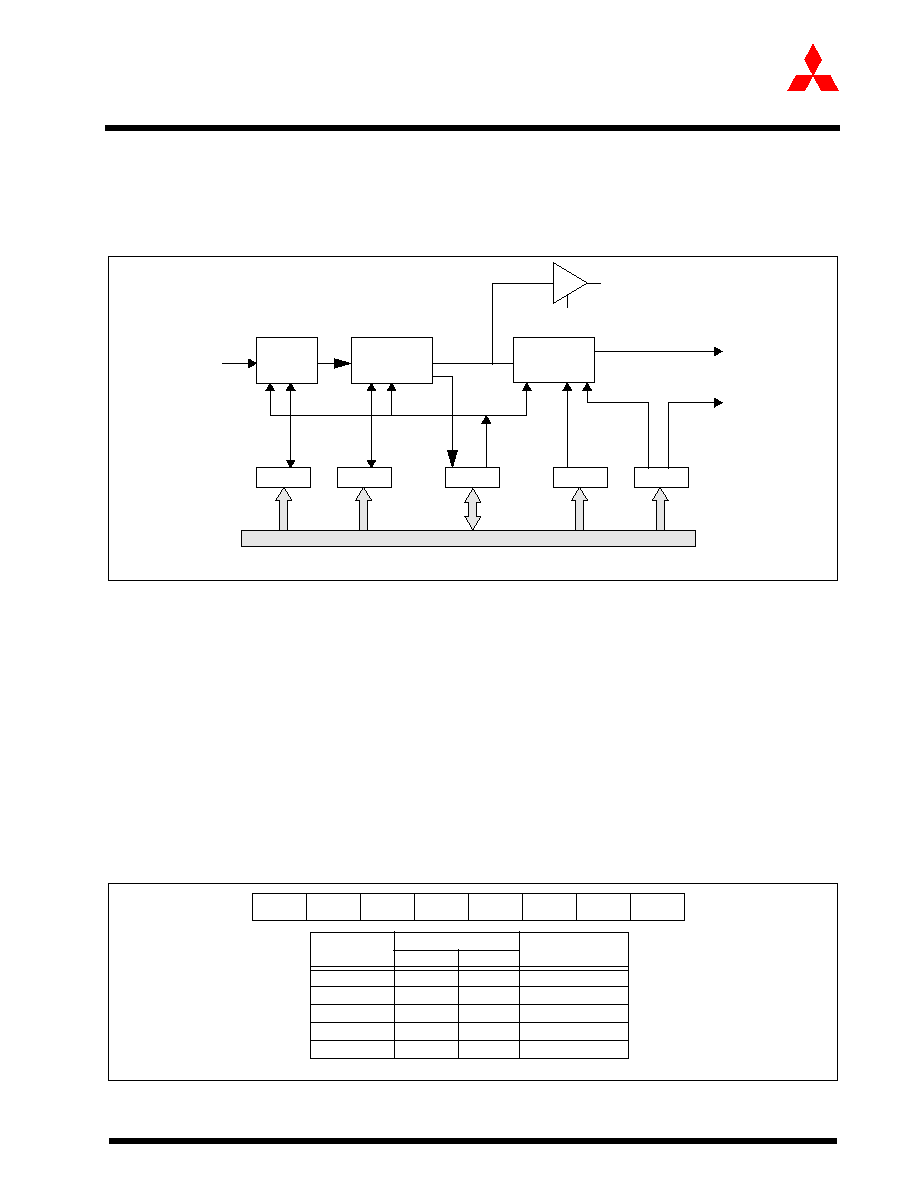
1-41
Mitsubishi microcomputers
M30240 Group
SINGLE-CHIP 16-BIT CMOS MICROCOMPUTER
Preliminary Specifications REV. E
Specifications in this manual are tentative and subject to change
Frequency Synthesizer Circuit
2.17 Frequency Synthesizer Circuit
The Frequency Synthesizer Circuit generates a 48MHz clock needed by the USB block and a clock f
SYN
that are both a multiple of the external input reference clock f(Xin). A block diagram of the circuit is shown
in Figure 1.23.
Figure 1.23: Frequency Synthesizer Circuit
The frequency synthesizer consists of a prescaler, frequency multiplier macro, a frequency divider
macro, and five registers, namely FSP, FSM, FSC, FSD, and FSCCR. Clock f(Xin) is prescaled down
using FSP to generate f
PIN
. f
PIN
is multiplied using FSM to generate an f
VCO
clock which is then divided
using FSD to produce the clock f
SYN
. The f
VCO
clock is optimized for 48 MHz operation and is buffered
and sent out of the frequency synthesizer block as signal f
USB
. This signal is used by the USB block.
2.17.1 Prescaler
Clock f
PIN
is a divided down version of clock f(Xin) (see Figure 1.24). The relationship between f
PIN
and the clock input to the prescaler f(Xin) is as follows:
� f
PIN
= f(Xin) / 2(n+1) where n is a decimal number between 0 and 254.
Setting FSP to 255 disables the prescaler and f
PIN
= f(Xin).
� Note: f(Xin) frequency below 1 MHz is not recommended.
Figure 1.24: Frequency Synthesizer Prescaler Register (FSP)
FSP
Data Bus
FSM
FSC
FSD
03DE
03DD
03DC
03DF
Frequency
Multiplier
Frequency
Divider
8 Bit
LS
8 Bit
f(Xin)
f
VCO
f
SYN
f
USB
Prescaler
8 Bit
f
PIN
FSCCR
FSCCR0
03DB
EN
USBC5
2
f
PIN
FSP
f(Xin)
Dec(n)
Hex(n)
12 MHz
255
FF
12.00 MHz
1 MHz
5
05
12.00 MHz
2 MHz
2
02
12.00 MHz
3 MHz
1
01
12.00 MHz
6 MHz
0
00
12.00 MHz
MSB
7
LSB
0
Bit 6
Bit 1
Bit 0
Bit 2
Bit 5
Bit 4
Bit 3
Bit 7
Access: R/W
Address: 03DE
16
Reset: FF
16
f(Xin)
/2(n+1) = f
PIN

1-42
Mitsubishi microcomputers
M30240 Group
SINGLE-CHIP 16-BIT CMOS MICROCOMPUTER
Preliminary Specifications REV. E
Specifications in this manual are tentative and subject to change
Frequency Synthesizer Circuit
2.17.2 Multiplier
Clock f
VCO
is a multiplied up version of clock f
PIN
(See Figure 1.25). The relationship between f
VCO
and the clock input to the multiplier (f
PIN
) from the prescaler is as follows:
� f
VCO
= f
PIN
x 2(
n+1) where n is the decimal equivalent of the value loaded in FSM.
Setting FSM to 255 disables the multiplier and f
VCO
= f
PIN
.
Note 1:
n must be chosen such that f
VCO
equals 48 MHz.
Note 2: Minimum f
PIN
is 1 MHz.
Figure 1.25: Frequency Synthesizer Multiply Register (FSM)
2.17.3 Divider
Clock f
SYN
is a divided down version of clock f
VCO
(See Figure 1.26). The relationship between f
SYN
and the clock input to the divider (f
VCO
) from the multiplier is as follows:
� f
SYN
= f
VCO
/ 2(m+1) where m is the decimal equivalent of the value loaded in FSD.
Setting FSD to 255 disables the divider and f
SYN
= f
VCO
.
Figure 1.26: Frequency Synthesizer Divide Register (FSD)
f
PIN
x 2(n+1) = f
VCO
f
PIN
FSM
f
VCO
Dec(n)
Hex(n)
1 MHz
33
4A
48.00 MHz
2 MHz
11
0B
48.00 MHz
4 MHz
5
05
48.00 MHz
6 MHz
3
03
48.00 MHz
12 MHz
1
01
48.00 MHz
MSB
7
LSB
0
Bit 6
Bit 1
Bit 0
Bit 2
Bit 5
Bit 4
Bit 3
Bit 7
Address: 03DD
16
Access: R/W
Reset: FF
16
f
VCO
/2(m+1) = f
SYN
f
VCO
FSD
f
SYN
Dec(m)
Hex(m)
48.00 MHz 1
01
12.00 MHz
48.00 MHz 127
7F
187.50 KHz
MSB
7
LSB
0
Bit 6
Bit 1
Bit 0
Address: 03DF
16
Access: R/W
Reset: FF
16
Bit 2
Bit 5
Bit 4
Bit 3
Bit 7

1-43
Mitsubishi microcomputers
M30240 Group
SINGLE-CHIP 16-BIT CMOS MICROCOMPUTER
Preliminary Specifications REV. E
Specifications in this manual are tentative and subject to change
Frequency Synthesizer Circuit
The FSC0 bit in the FSC Control Register enables the frequency synthesizer block. When disabled
(FSC0 = "0"), f
VCO
is held at either a high or low state. When the frequency synthesizer control bit is
active (FSC0 = "1"), a lock status (LS = "1") indicates that f
SYN
and f
VCO
are the correct frequency. The
LS and FSCO control bits in the FSC Control register are shown in Figure 1.27.
When using the frequency synthesizer, a low-pass filter must be connected to the LPF pin.
Once the frequency synthesizer is enabled, a delay of 2-5ms is recommended before the output of the
frequency synthesizer is used. This is done to allow the output to stabilize. It is also recommended that
none of the registers be modified once the frequency synthesizer is enabled as it will cause the output
to be temporarily (2-5ms) unstable. The MCU clock source is selected via the Frequency Synthesizer
Clock Control register (FSCCR). See Figure 1.28.
Note: None of the registers must be written to once the frequency synthesizer is enabled and used as
the system clock source (FSCCR register, address 03DB
16
, bit `0' set to `1') because it will cause the
output of the PLL to freeze. Switch system back to f(X
IN
) and disable before modifying PLL registers.
Figure 1.27: Frequency Synthesizer Control Register (FSC)
Figure 1.28: Frequency Synthesizer Clock Control Register (FSCCR)
Frequency Synthesizer Control Register
Symbol
Address
When reset
FSC
03DC
16
60
16
Bit name
Bit symbol
b7
b6
b5
b4
b3
b2
b1
b0
0 : Disable
1 : Enabled
VCO0
FSE
VCO Gain Control
Function
Bit 2
Bit 1
0
0:
Lowest Gain (Note 1)
0
1:
Low Gain
1
0:
High Gain
1
1:
Highest Gain
Frequency Synthesizer Enable
W
R
Reserved bit
Must always be set to "0"
VCO1
CHG0
CHG1
LPF Current Control
Bit 6
Bit 5
0
0:
Disabled
0
1:
Low Current
1
0:
Intermediate Current (Note 1)
1
1:
High Current
LS
Frequency Synthesizer
Lock Status
0:
Unlocked
1:
Locked
Note 1: Recommended
0 0
Frequency Synthesizer Clock Control Register
Symbol
Address
When reset
FSCCR
03DB
16
00
16
Bit name
Bit symbol
b7
b6
b5
b4
b3
b2
b1
b0
0 : Xin
1 : fsyn
FSCCR0
Function
W
R
Reserved
Must always be set to "0"
Clock source selection
0 0 0 0 0 0 0

1-44
Mitsubishi microcomputers
M30240 Group
SINGLE-CHIP 16-BIT CMOS MICROCOMPUTER
Preliminary Specifications REV. E
Specifications in this manual are tentative and subject to change
Universal Serial Bus
2.18 Universal Serial Bus
The Universal Serial Bus (USB) has the following features:
� Complete USB Specification (version 1.1) Compatibility
� Error-handling capabilities
� FIFOs:
� Endpoint 0:
IN/OUT 32-byte
� Endpoint 1:
IN 128-byte
OUT 128-byte
� Endpoint 2:
IN 32-byte
OUT 32-byte
� Endpoint 3:
IN 32-byte
OUT 32-byte
� Endpoint 4:
IN 32-byte
OUT 32-byte
� Nine endpoints - control endpoint (Endpoint 0 - bi-directional) plus four IN and four OUT
endpoints
� Complete device configuration
� Support of all device commands
� Supports of full-speed functions
� Support of all USB transfer types:
� Isochronous
� Bulk
� Control
� Interrupt
� Suspend/Resume operation
� On-chip USB transceiver with voltage converter
� Start-of-frame interrupt and output pin
2.18.1 USB Function Control Unit (USB FCU)
The implementation of the USB by this device is accomplished chiefly through the device's USB
Function Control Unit (See Figure 1.29). The Function Control Unit's overall purpose is to handle the
USB packet protocol layer. The Function Control Unit notifies the MCU that a valid token has been
received. When this occurs, the data portion of the token is routed to the appropriate FIFO. The MCU
transfers the data to, or from, the host by interacting with that endpoint's FIFO and CSR register.
The USB Function Control Unit is composed of five sections:
� Serial Interface Engine (SIE)
� Generic Function Interface (GFI)
� Serial Engine Interface Unit (SIU)
� Microcontroller Interface (MCI)
� USB Transceiver
2.18.1.1 Serial Interface Engine
The SIE interfaces to the USB serial data and handles deserialization/serialization of data, NRZI encoding
decoding, clock extraction, CRC generation and checking, bit stuffing, and other items pertaining to the USB
protocol such as handling inter-packet time-outs and packet ID (PID) decoding.
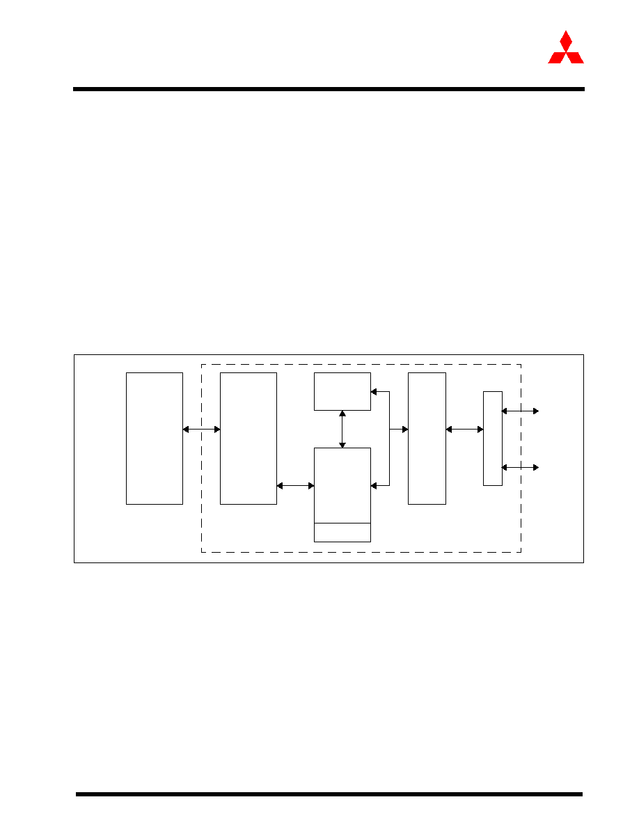
1-45
Mitsubishi microcomputers
M30240 Group
SINGLE-CHIP 16-BIT CMOS MICROCOMPUTER
Preliminary Specifications REV. E
Specifications in this manual are tentative and subject to change
Universal Serial Bus
2.18.1.2 Generic Function Interface
The GFI handles all USB standard requests from the host through the control endpoint (endpoint zero), han-
dles Bulk, Isochronous and Interrupt transfers through endpoints 1-4. The GFI handles read pointer reversal
for re-transmission the current data set; write pointer reversal for reception of the last data set again and data
toggle synchronization.
2.18.1.3 Serial Engine Interface Unit
The SIU block decodes the Address and Endpoint fields from the USB host.
2.18.1.4 Microcontroller Interface
The MCI block handles the Microcontroller interface and performs address decoding and synchronization of
control signals.
2.18.1.5 USB Transceiver
The USB transceiver, designed to interface with the physical layer of the USB, is compliant with the USB
Specification (version 1.1) for full-speed devices. It consists of two 6-ohm drivers, a receiver, and Schmitt trig-
gers for single-ended receive signals.
The transceiver also includes a voltage converter. The voltage converter can supply 3.0 - 3.6V to the trans-
mitter when the rest of the chip (CPU, USB FCU) operates at 4.15 - 5.25V. To enable the voltage converter,
set bit 4 of the USB Control Register (USBC) to a "1". To disable the voltage converter, set bit 4 of the USBC
to a "0". Refer to Section 5.4 "USB Transceiver" for more detailed information.
Figure 1.29: USB Function Control Unit Block Diagram
2.18.2 USB Interrupts
There are five USB interrupts in this device:
�
USB Function interrupt
�
USB Reset interrupt
�
USB Suspend interrupt
�
USB Resume interrupt
�
USB Start-of-Frame (SOF) interrupt.
The first four interrupts are used to control the data flow and USB power. The SOF interrupt is used to monitor
the transfer of isochronous (ISO) data. Each of the five USB interrupts is enabled by setting the corresponding
bit in the Interrupt Control Register of the Interrupt Control Unit. Because the USB Function Interrupt has mul-
tiple interrupt sources, another level of enabling is within the USB Interrupt Registers 1 & 2.
CPU
MCI
SIU
GFI
FIFOs
SIE
T
r
ansceiv
er
D
+
D
-

1-46
Mitsubishi microcomputers
M30240 Group
SINGLE-CHIP 16-BIT CMOS MICROCOMPUTER
Preliminary Specifications REV. E
Specifications in this manual are tentative and subject to change
Universal Serial Bus
2.18.2.1 USB Function Interrupt
The USB Function Interrupt can be triggered by 10 sources; many of these may be cause by several different
events. Interrupt status flags associated with each source are contained in USBIS1 and USBIS2.
Endpoints 1-4 have two interrupt status flags associated with it to control data transfer or to report a STALL/
UNDER_RUN/OVER RUN condition.
The USB Endpoint x Out Interrupt Status Flag is set when
�
USB FCU successfully receives a packet of data OR
�
USB FCU sets the FORCE_STALL bit or OVER_RUN bit of the Endpoint x OUT CSR.
The USB Endpoint x In Interrupt Status is set when
�
USB FCU successfully sends a packet of data OR
�
USB FCU sets the UNDER_RUN bit of the Endpoint x IN CSR.
The USB Endpoint 0 (control endpoint) has one interrupt status bit associated with it to control data transfer
or report a STALL condition.
The USB Endpoint 0 Interrupt Status Flag is set when
�
USB FCU successfully receives/sends a packet of data
�
Sets the SETUP_END bit or the FORCE_STALL bit, OR clears the DATA_END bit in the Endpoint 0 IN
CSR.
The Overrun/Underrun Interrupt Status Flag is set when (applicable to endpoints used for isochronous data
transfer)
�
Overrun condition occurs in a endpoint (CPU is too slow to unload the data from the FIFO), OR
�
Underrun condition occurs in an endpoint (CPU is too slow to load the data to the FIFO).
Each endpoint interrupt and overrun/underrun interrupt is enabled by setting the corresponding bit in the USB
Interrupt Enable Register 1 and 2.
2.18.2.2 USB Reset Interrupt
The USB Reset Interrupt Status Flag is set when the USB FCU sees a SE0 present on D+/D- for at least
2.5
�
s. When this bit is set, all USB internal registers except INTST13 (bit5 of USBIS2) are reset to their default
values. INTST13, the USB reset Interrupt Status Flag, is set to a "1" when the USB Reset is detected.
When the CPU recognizes a USB Reset Interrupt, it needs to re initialize the USB FCU so that the USB op-
eration can behave properly. It must also clear INTST13 by writing a "1" to this bit to allow a USB Reset Inter-
rupt request to occur the next time a USB Reset is detected.
Register RSTIC contains the USB Reset Interrupt's request bit and its interrupt priority select bits which are
used to enable the interrupt and set its software priority level.
2.18.2.3 USB Suspend and Resume Interrupts
The USB Suspend Interrupt is set when the USB FCU does not detect any bus activity on D+/D- (in J-state)
for at least 3ms.
The USB Suspend Signaling Interrupt Status Flag (INTST15, bit 7 of USBIS2) is set to a "1" when the USB
Suspend is detected. The CPU must clear INTST15 by writing a "1" to this bit to allow a USB Suspend Interrupt
request to occur the next time a USB Suspend is detected.
The USB Resume Signaling Interrupt Status Flag is set when a USB FCU is in the suspend state and detects
non-idle signaling on the D+/D-.
Register SUSPIC contains the USB Suspend Interrupt's request bit and its interrupt priority select bits which
are used to enable the interrupt and set its software priority level.
The USB Resume Interrupt request is set when the USB FCU is in the suspend state and detects non-idle
signaling on D+/D-.
The USB Signaling Interrupt Status Flag (INTST14, bit 6 of USBIS2) is set to a "1" when the USB Resume is
detected. The CPU must clear INTST14 by writing a "1" to this bit to allow a USB Resume Interrupt request
to occur the next time a USB Resume is detected.
Register RSMIC contains the USB Resume Interrupt's request bit and its interrupt priority select bits, which
are used to enable the interrupt an set its software priority level.

1-47
Mitsubishi microcomputers
M30240 Group
SINGLE-CHIP 16-BIT CMOS MICROCOMPUTER
Preliminary Specifications REV. E
Specifications in this manual are tentative and subject to change
Universal Serial Bus
2.18.2.4 USB SOF Interrupt
The USB SOF (Start-Of-Frame) Interrupt is used to control the transfer of isochronous data. The USB FCU
generates a USB SOF Interrupt request when a start-of-frame packet is received.
Register SOFIC contains the USB SOF Interrupt's request bit and its interrupt priority select bits, which are
used to enable the interrupt and set its software priority level.
2.18.3 USB Endpoint FIFOs
The USB FCU has an IN (transmit) FIFO and an OUT (receive) FIFO for each endpoint. Each endpoint (ex-
cept endpoint 0) can be configured to support either single packet mode (in which only a single data packet
is allowed to reside in the endpoint's FIFO) or dual packet mode (in which up to two data packets are allowed
to reside in the endpoint's FIFO). Dual packet mode provides support for back-to-back transmission or back-
to-back reception. The mode is automatically determined by the MAXP value. When MAXP > 1/2 of the end-
point's FIFO size, single packet mode is set. When MAXP <= 1/2 of the endpoint's FIFO size, dual packet
mode is set.
In the event of a bad transmission/reception, the USB FCU handles all the FIFO read/write pointer reversal
and data set management tasks required.
Throughout this specification, the terms "IN FIFO" and "OUT FIFO" usually refer to the FIFOs associated with
a specific endpoint.
2.18.3.1 IN (Transmit) FIFOs
The CPU/DMA writes data to the endpoint's IN FIFO location specified by the FIFO write pointer, which auto-
matically increments by "1" after a write. The CPU/DMA should only write data to the IN FIFO when the
IN_PKT_RDY bit of the associated IN CSR is a "0".
�
Endpoint 0 IN FIFO Operation:
The CPU writes a "1" to the IN_PKT_RDY bit of Endpoint 0 CSR after it finishes writing a packet of data to the
IN FIFO. The USB FCU clears the IN_PKT_RDY bit after the packet has been successfully transmitted to the
host (i.e., ACK is received from the host) or the SETUP_END bit of the IN CSR is set to a "1".
�
Endpoint 1-4 IN FIFO Operation when AUTO_SET (bit 7 of Endpoint x IN CSR) = "0" (disabled):
MAXP > 1/2 of the IN FIFO size: The CPU writes a "1" to the IN_PKT_RDY bit of the associated IN CSR after
the CPU/DMAC finishes writing a packet of data to the IN FIFO. The USB FCU clears the IN_PKT_RDY bit
after the packet has been successfully transmitted to the host (which is assumed for isochronous transfers
and is concluded when an ACK is received from the host for non-isochronous transfers).
MAXP <= 1/2 of the IN FIFO size: The CPU writes a "1" to the IN_PKT_RDY bit of the associated IN CSR
after the CPU/DMAC finishes writing a packet of data to the IN FIFO. The USB FCU clears the IN_PKT_RDY
bit as soon as the IN FIFO is ready to accept another data packet. (The FIFO can hold up to two data packets
at the same time in this configuration for back-to-back transmission.)
�
Endpoint 1-4 IN FIFO Operation when AUTO_SET (bit 7 of Endpoint x IN CSR) = "1" (enabled):
MAXP > 1/2 of the IN FIFO size: When the number of bytes of data equal to the MAXP (maximum packet size)
has been written to the IN FIFO by the CPU/DMAC, the USB FCU sets the IN_PKT_RDY bit of the associated
IN CSR to a "1" automatically. The USB FCU clears the IN_PKT_RDY bit after the packet has been success-
fully transmitted to the host (which is assumed for isochronous transfers and is concluded when an ACK is
received from the host for non-isochronous transfers).
MAXP <= 1/2 of the IN FIFO size: When the number of bytes of data equal to the MAXP (maximum packet
size) has been written to the IN FIFO by the CPU/DMAC, the USB FCU sets the IN_PKT_RDY bit to a "1"
automatically. The USB FCU clears the IN_PKT_RDY bit as soon as the IN FIFO is ready to accept another
data packet. (The FIFO can hold up to two data packets at the same time in this configuration for back-to-back
transmission.)
A software or a hardware flush causes the USB FCU to act as if a packet has been successfully transmitted
out to the host. When there is one packet in the IN FIFO, a flush causes the IN FIFO to be empty. When there
are two packets in the IN FIFO, a flush causes the older packet to be flushed out from the IN FIFO. A flush
also updates the IN FIFO status bits IN_PKT_RDY and TX_NOT_EMPTY of the associated IN CSR.

1-48
Mitsubishi microcomputers
M30240 Group
SINGLE-CHIP 16-BIT CMOS MICROCOMPUTER
Preliminary Specifications REV. E
Specifications in this manual are tentative and subject to change
Universal Serial Bus
The status of endpoint 1-4 IN FIFOs for both of the above cases can be obtained from the IN CSR of the cor-
responding IN FIFO as shown in Table 1.13 .
2.18.3.2 Out (Receive) FIFOs
The USB FCU writes data to the endpoint's OUT FIFO location specified by the FIFO write pointer, which au-
tomatically increments by one after a write. When the USB FCU has successfully received a data packet, it
sets the OUT_PKT_RDY bit of the corresponding OUT CSR to a "1". The CPU/DMAC should only read data
from the OUT FIFO when the OUT_PKT_RDY bit of the OUT CSR is a "1".
�
Endpoint 0 OUT FIFO Operation:
The USB FCU sets the OUT_PKT_RDY bit to a "1" after it has successfully received a packet of data from the
host. The CPU sets bit SERVICED_OUT_PKT_RDY to a "1" to clear the OUT_PKT_RDY bit after the packet
of data has been unloaded from the OUT FIFO by the CPU.
�
Endpoint 1-4 OUT FIFO Operation when AUTO_CLR (bit 7 of Endpoint x OUT CSR) = "0" (disabled):
MAXP > 1/2 of the OUT FIFO size: The USB FCU sets the OUT_PKT_RDY bit of the associated IN CSR to
a "1" after it has successfully received a packet of data from the host. The CPU writes a "0" to the
OUT_PKT_RDY bit after the packet of data has been unloaded from the OUT FIFO by the CPU/DMAC.
MAXP <= 1/2 of the OUT FIFO size: The USB FCU sets the OUT_PKT_RDY bit of the associated IN CSR to
a "1" after it has successfully received a packet of data from the host. The CPU writes a "0" to the
OUT_PKT_RDY bit after the packet of data has been unloaded from the OUT FIFO by the CPU/DMAC. If an-
other packet is in the OUT FIFO, the OUT_PKT_RDY bit will be set to a "1" again almost immediately (such
that it may appear that the OUT_PKT_RDY bit remains a "1"). In this configuration, the FIFO can store up to
two data packets at the same time for back-to-back reception.
�
Endpoint 1-4 OUT FIFO Operation when AUTO_CLR (bit 7 of Endpoint x OUT CSR) = "1" (enabled):
MAXP > 1/2 of the OUT FIFO size: The USB FCU sets the OUT_PKT_RDY bit of the associated IN CSR to
a "1" after it has successfully received a packet of data from the host. The USB FCU clears the
OUT_PKT_RDY bit to a "0" automatically when the number of bytes of data equal to the MAXP (maximum
packet size) has been unloaded from the OUT FIFO by the CPU/DMAC.
MAXP <= 1/2 of the OUT FIFO size: The USB FCU sets the OUT_PKT_RDY bit of the associated IN CSR to
a "1" after it has successfully received a packet of data from the host. The USB FCU clears the
OUT_PKT_RDY bit to a "0" automatically when the number of bytes of data equal to the MAXP (maximum
packet size) has been unloaded from the OUT FIFO by the CPU/DMAC. If another packet is in the OUT FIFO,
the OUT_PKT_RDY bit will be set to a "1" again almost immediately (such that it may appear that the
OUT_PKT_RDY bit remains a "1"). In this configuration, the FIFO can store up to two data packets at the same
time for back-to-back reception.
A software flush causes the USB FCU to act as if a packet has been unloaded from the OUT FIFO. If there is
one packet in the OUT FIFO, a flush will cause the OUT FIFO to be empty. If there are two packets in the OUT
FIFO, a flush will cause the older packet to be flushed out from the OUT FIFO.
Table 1.13:
TA FIFO Status
IN_PKT_RDY
TX_NOT_EMPTY
IN FIFO Status
0
0
No data packet in IN FIFO
0
1
One data packet in IN FIFO if MAXP <= 1/2 of the FIFO size./
Invalid when MAXP>1/2 of the FIFO size
1
0
Invalid
1
1
Two data packets in IN FIFO when MAXP <=1/2 of the FIFO size
One data packet in IN FIFO when MAXP > 1/2 of the FIFO size

1-49
Mitsubishi microcomputers
M30240 Group
SINGLE-CHIP 16-BIT CMOS MICROCOMPUTER
Preliminary Specifications REV. E
Specifications in this manual are tentative and subject to change
Universal Serial Bus
2.18.3.3 Interrupt Endpoints:
Any endpoint can be used for interrupt transfers. For normal interrupt transfers, the interrupt transactions be-
have the same as bulk transactions, i.e., no special setting is required. The IN endpoints may also be used to
communicate rate feedback information for certain types of isochronous functions. This is done by setting the
INTPT bit in the IN CSR register of the corresponding endpoint.
The following outlines the operation sequence for an IN endpoint used to communicate rate feedback infor-
mation:
1. Set MAXP > 1/2 of the endpoint's FIFO size;
2. Set INTPT bit of the IN CSR;
3. Flush the old data in the FIFO;
4. Load interrupt status information and set IN_PKT_RDY bit in the IN CSR;
5. Repeat steps 3 & 4 for all subsequent interrupt status updates.
2.18.4 USB Special Function Registers
The MCU controls USB operation through the use of special function registers (SFR). This section de-
scribes each USB related SFR. Some USB special function registers have a mix of read/write, read
only, and write only register bits. Additionally, the bits may be configured to allow the user to write only
a "0" or a "1" to individual bits.
� When accessing these registers, writing a "0" to a register that can only be set to a "1" by the CPU
has no effect on that register bit.
� Writing a "1" to a register that can only be set to a "0" by the CPU has not effect on that register bit.
Each figure and description of the special function registers details this operation.
All USB Special Function Registers, with the exception of USB Attach/Detach (001F
16
) and USB con-
trol (000C
16
) must use byte access. Work access is prohibited for USB internal registers (0300
16
-
033C
16
).
The contents of all USB Special Functions Registers, including USB Attach/Detach and USB Control,
are preserved on a software reset.
2.18.4.1 USB Attach/Detach Register
The USB Attach / Detach Register is shown in Figure 1.30. The register is used to attach and detach the USB
function from a USB host without physically disconnecting the USB cable. This functionality is enabled by set-
ting P83_SECOND to a "1". Doing this forces P83 to operate as a pull-up for D+ (through an external 1.5k
ohm resistor). The port driver is tri-stated and a "1" is always read from the port bit in this mode. When the
ATTACH/DETACH bit is a "1" (and P83_SECOND is a "1"), P83 is driven with the voltage on EXTCAP, caus-
ing D+ to be pulled up and the host to detect an attach. When the ATTACH/DETACH bit is a "0" (and
P83_SECOND is a "1"), P83 is tri-stated, causing D+ to be pulled down (through the cable and 15k ohm re-
sistor on the host/hub side) and a detach to be registered by the host. A 1.5k ohm pull-up resistor must be
connected externally from P83 to D+ when this functionality is used. When it is not used, the 1.5k ohm resistor
should be placed between EXTCAP and D+.
Figure 1.30: USB Attach/Detach Register
USB Attach/Detach Register
Symbol
Address
When reset
USBAD
001F16
0016
Bit name
Bit symbol
b7 b6 b5 b4 b3 b2 b1 b0
0 : Normal mode for Port 8_3
1 : Forces Port 8_3 to operate as pull up for D+.
P83_2nd
Function
Reserved
Must always be set to "0"
Port 83-Second
Attach/
Detach
Attach/Detach
0 : Tri-states, P8_3 causing the host to detect a detach
1 : Drives P8_3 with voltage on EXTCAP, causing the host
to detect an attach
W
R
0 0 0 0 0 0

1-50
Mitsubishi microcomputers
M30240 Group
SINGLE-CHIP 16-BIT CMOS MICROCOMPUTER
Preliminary Specifications REV. E
Specifications in this manual are tentative and subject to change
Universal Serial Bus
2.18.4.2 USB Control Register
The USB Control Register, shown in Figure 1.31, is used to control the USB FCU. This register is not reset
by a USB reset signaling. After the USB is enabled (USBC7 set to "1"), a minimum delay of 250ns (three 12
MHz clock periods) is needed before performing any other USB register read/write operations.
Figure 1.31: USB Control Register
2.18.4.3 USB Function Address Register
The USB Function Address Register, shown in Figure 1.32, maintains the 7-bit USB address assigned by the
host. The USB FCU uses this register value to decode USB token packet addresses. At reset, when the de-
vice is not yet configured, the value is 00
16
. For the procedures on how to update this register, refer to Appli-
cation Notes USB Consecutive Set Address.
Figure 1.32: USB Function Address Register
USB Control Register
Symbol
Address
When reset
USBC
000C16
0016
Bit name
Bit symbol
b7
b6
b5
b4
b3
b2
b1
b0
Function
W
R
Must always be set to "0"
Reserved
USBC3
USBC4
USBC5
USBC6
USBC7
Tranceiver voltage converter
High/Low current mode selection
USB tranceiver voltage converter
enable bit
USB clock enable bit
USB SOF port select bit
USB enable bit
0: High current mode (Note 1)
1: Low current mode (Note 2)
0: Disabled
1: Enabled
0: Disabled
1: Enabled
0: Disabled (Note 3)
1: Enabled
0: Disabled (Note 4)
1: Enabled
Note 1: For USB normal operation
Note 2: For USB suspend operation
Note 3: P8
6
is used as GPIO pin
Note 4: All USB internal registers are held at their default values.
0 0 0
Function Address Register
Symbol
Address
When reset
USBA
0300
16
00
16
Bit name
Bit symbol
b7
b6
b5
b4
b3
b2
b1
b0
FUNAD0-6
Function
W
R
Reserved
Must always be set to "0"
7-bit programmable
Function Address
Function Address
0

1-51
Mitsubishi microcomputers
M30240 Group
SINGLE-CHIP 16-BIT CMOS MICROCOMPUTER
Preliminary Specifications REV. E
Specifications in this manual are tentative and subject to change
Universal Serial Bus
2.18.4.4 The USB Power Management Register
The USB Power Management Register, shown in Figure 1.33, is used for power management in the USB
FCU.
�
SUSPEND Detection Flag:
When the USB FCU does not detect any bus activity on D+/D- for at least 3ms (and D+/D- are in the J-state),
it sets the Suspend Detection Flag and generates an interrupt. This bit is cleared when signaling from the host
is detected on D+/D- (which sets the Resume Detection Flag and generates an interrupt), or the Remote
Wake-up Bit is set and then cleared by the CPU. If the USB clock was disabled during the suspend state, the
SUSPEND Detection Flag is not cleared until after the USB clock is re-enabled.
�
RESUME Detection Flag:
When the USB FCU is in the suspend state and detects activity on D+/D- from the host, it sets the Resume
Detection Flag and generates an interrupt. The CPU writes a "1" to INTST14 (bit 6 of USB Interrupt Status
Register 2) to clear this flag.
�
WAKEUP Control Bit:
The CPU writes a "1" to the WAKEUP Control Bit for remote wake-up. While this bit is set and the USB FCU
is in suspend mode, resume signaling is sent to the host. The CPU must keep this bit set for a minimum of
10ms and a maximum of 15ms before writing a "0" to this bit.
Figure 1.33: USB Power Management Register
USB Power Management Register
Symbol
Address
When reset
USBPM
0301
16
00
16
Bit name
Bit symbol
b7
b6
b5
b4
b3
b2
b1
b0
Function
W
R
Reserved
Must always be set to "0"
SUSPEND
RESUME
WAKEUP
USB Suspend Detection Flag
USB Resume Detection Flag
USB Remote Wakeup Bit
0 : No USB suspend signal detected
1 : USB suspend signal detected
0 : No USB resume signal detected
1 : USB resume signal detected
0 : End remote resume signaling
1 : Remote resume signaling (Note 2)
Note 1: Write "0" only or Read
Note 2: If SUSPEND = "1"
Note 1
Note 1
0 0 0 0 0

1-52
Mitsubishi microcomputers
M30240 Group
SINGLE-CHIP 16-BIT CMOS MICROCOMPUTER
Preliminary Specifications REV. E
Specifications in this manual are tentative and subject to change
Universal Serial Bus
2.18.4.5 USB Interrupt Status Registers 1 and 2
USB Interrupt Status Registers 1 and 2, shown in Figure 1.34 and Figure 1.35, are used to indicate the con-
dition that caused a USB function interrupt and USB Reset, Suspend and Resume Interrupts to the CPU. A
"1" indicates the corresponding condition caused an interrupt. The USB Interrupt Status Register bits can be
cleared by writing a "1" to the corresponding bit.
INTST0 is set to a "1" by the USB FCU when (in Endpoint 0 CSR):
�A packet of data is successfully received (EP0CSR0 - OUT_PKT_RDY is set by the USB FCU)
�A packet of data is successfully sent (EP0CSR - IN_PKT_RDY is cleared by the USB FCU)
�EP0CSR3 (DATA_END) bit is cleared by the USB FCU
�EP0CSR4 (FORCE_STALL) bit is set by the USB FCU
�EP0CSR5 (SETUP_END) bit is set by the USB FCU
INTST2, INTST4, INTST6 or INTST8 is set to a "1" by the USB FCU when (in Endpoint x IN CSR):
�A packet of data is successfully sent (INXCSR0 - IN_PKT_RDY is cleared by the USB FCU)
�INXCSR1 (UNDER_RUN) bit is set by the USB FCU
INTST3, INTST5, INTST7 or INTST9 is set to a "1" by the USB FCU when (in Endpoint xOUT CSR):
�A packet of data is successfully received (OUTXCSR0 - OUT_PKT_RDY is set by the USB FCU)
�OUTXCSR1 (OVER_RUN) bit is set by the USB FCU
�OUTXCSR4 (FORCE_STALL) bit is set by the USB FCU
INTST12 is set to a "1" by the USB FCU when an overrun or underrun condition occurs in any of the endpoints.
INTST13 is set to a "1" by the USB FCU when a USB reset signaling from the host is received. All internal
register bits except this bit are reset to their default values when the USB reset is received.
INTST14 is set to a "1" by the USB FCU when the USB FCU is in the suspend state and non-idle signaling is
received from D+/D-.
INTST15 is set to a "1" by the USB FCU when D+/D- are in the idle state for more than 3ms.
Figure 1.34: USB Interrupt Status Register 1
USB Interrupt Status Register 1
Symbol
Address
When reset
USBIS1
0302
16
00
16
Bit name
Bit symbol
b7
b6
b5
b4
b3
b2
b1
b0
Function
W
R
Reserved
Must always be set to "0"
INTST0
INTST2
INTST3
INTST4
INTST5
INTST6
INTST7
USB Endpoint 0 Interrupt
Status Flag
USB Endpoint 1 IN
Interrupt Status Flag
USB Endpoint 1 OUT
Interrupt Status Flag
USB Endpoint 2 IN
Interrupt Status Flag
USB Endpoint 2 OUT
Interrupt Status Flag
USB Endpoint 3 IN
Interrupt Status Flag
USB Endpoint 3 OUT
Interrupt Status Flag
0 : No interrupt request issued
1 : Interrupt request issued
0 : No interrupt request issued
1 : Interrupt request issued
0 : No interrupt request issued
1 : Interrupt request issued
0 : No interrupt request issued
1 : Interrupt request issued
0 : No interrupt request issued
1 : Interrupt request issued
0 : No interrupt request issued
1 : Interrupt request issued
0 : No interrupt request issued
1 : Interrupt request issued
0
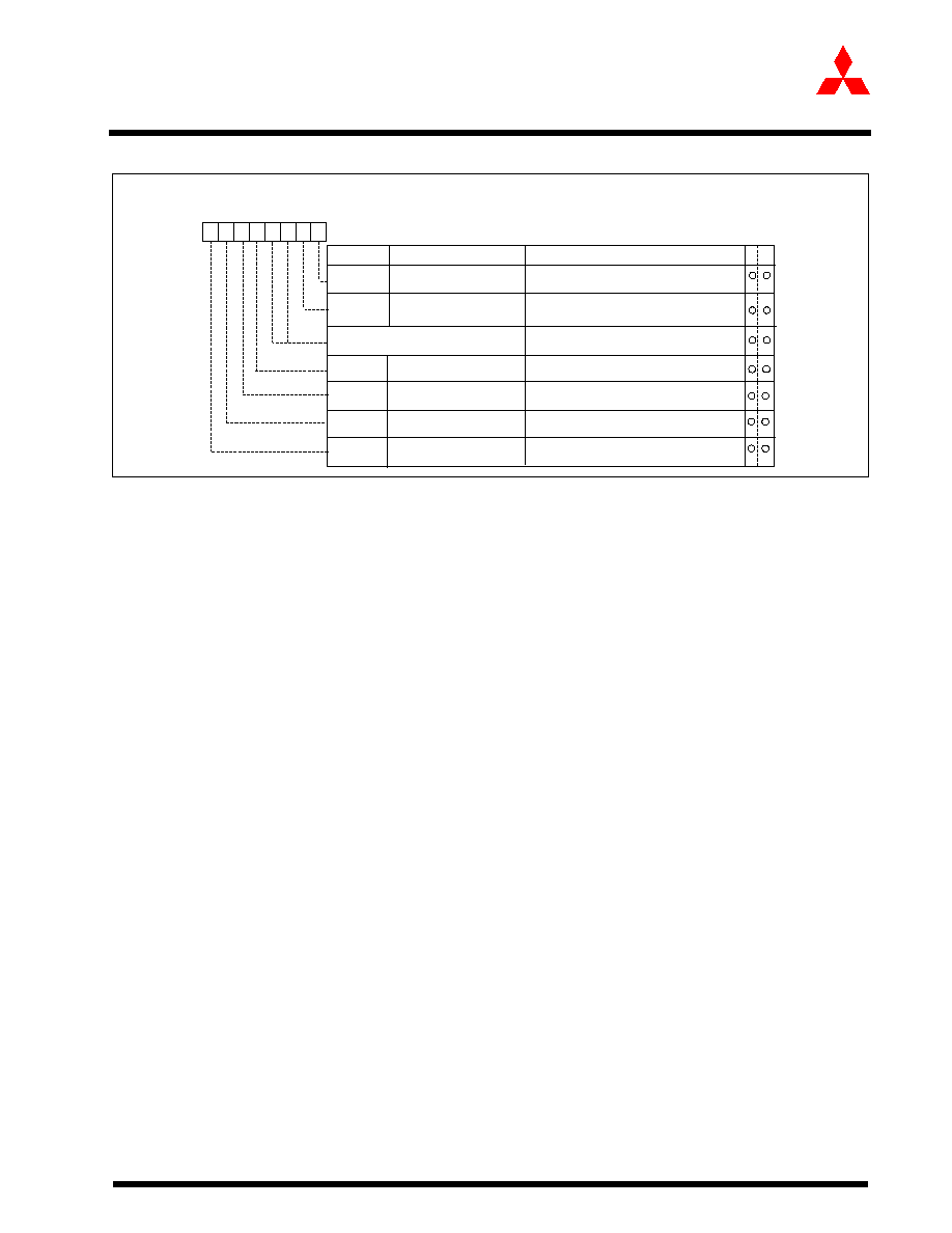
1-53
Mitsubishi microcomputers
M30240 Group
SINGLE-CHIP 16-BIT CMOS MICROCOMPUTER
Preliminary Specifications REV. E
Specifications in this manual are tentative and subject to change
Universal Serial Bus
Figure 1.35: USB Interrupt Status Register 2
2.18.4.6 Clearing of the USB Interrupt Status Registers
The USB Interrupt Status Register 1 and 2 are used to indicate pending interrupts for a given source. The
USB FCU sets the interrupt status bits. The CPU writes a "1" to each status bit to clear it.
Because the USB Function Interrupt has multiple sources that can generate an interrupt, it is recommended
that the user first read the two status registers and store them in variables then write back the same value for
clearing all the existing interrupts that were pending when the status registers were read. This procedure pre-
vents any interrupt that occurs after the status registers are read from being cleared by the `write-back' oper-
ation. The CPU must read, then write both status registers, writing to status register 1 first and status register
2 second to guarantee proper operation. The upper three bits of the value written back to USBIS2 should al-
ways be "000" to prevent any of the USB Reset, Suspend and Resume Status Flags from being cleared.
The USB Reset, Suspend and Resume Status Flags are contained in USBIS2 along with the USB Endpoint
4 In/Out Interrupt Status Flags and the USB Overrun/Underrun Interrupts Status Flag. Because the flags are
not all sources for the same interrupt, use caution when clearing one or more of the flags to avoid inadvertently
clearing other flags. The Reset, Suspend and Resume Status Flags should be cleared individually by writing
a byte value with at "1" only at the position corresponding to the flag to be cleared. The USB Endpoint 4 In/
Out Interrupt status Flags and the USB Overrun/Underrun Interrupt Status Flag should be cleared as de-
scribed in the preceding paragraph because they are sourced for the USB Function Interrupt.
"Read-modify-write' instructions, such as "BCLR' and `BSET', should not be used to clear any of the interrupt
status bits in USBIS1 or USBIS2. Using these instructions could cause pending interrupts to be cleared with-
out the firmware's knowledge.
2.18.4.7 The USB Function Interrupt Enable Registers 1 and 2
The USB Function Interrupt Enable Registers 1 and 2, shown in Figure 1.36 and Figure 1.37, are used to en-
able the corresponding interrupt status conditions that can generate a USB Function Interrupt. When the bit
to a corresponding interrupt condition is "0", that condition does not generate a USB function interrupt. When
the bit is a "1", that condition can generate a USB function interrupt. At reset, all USB function interrupt status
conditions are enabled.
USB Interrupt Status Register 2
Symbol
Address
When reset
USBIS2
0303
16
00
16
Bit name
Bit symbol
b7
b6
b5
b4
b3
b2
b1
b0
Function
W
R
Reserved
Must always be set to "0"
INTST8
INTST9
USB Endpoint 4 IN
Interrupt Status Flag
USB Endpoint 4 OUT
Interrupt Status Flag
USB Overrun/Underrun
Interrupt Status Flag
USB Reset
Interrupt Status Flag
USB Resume Signaling
Interrupt Status Flag
USB Suspend Signaling
Interrupt Status Flag
0 : No interrupt request issued
1 : Interrupt request issued
0 : No interrupt request issued
1 : Interrupt request issued
0 : No interrupt request issued
1 : Interrupt request issued
0 : No interrupt request issued
1 : Interrupt request issued
0 : No interrupt request issued
1 : Interrupt request issued
0 : No interrupt request issued
1 : Interrupt request issued
Reserved
INTST12
INTST13
INTST14
INTST15
0 0

1-54
Mitsubishi microcomputers
M30240 Group
SINGLE-CHIP 16-BIT CMOS MICROCOMPUTER
Preliminary Specifications REV. E
Specifications in this manual are tentative and subject to change
Universal Serial Bus
Figure 1.36: USB Interrupt Enable Register 1
Figure 1.37: USB Interrupt Enable Register 2
USB Interrupt Enable Register 1
Symbol
Address
When reset
USBIE1
0304
16
FF
16
Bit name
Bit symbol
b7
b6
b5
b4
b3
b2
b1
b0
Function
W
R
Reserved
Must always be set to "1"
INTEN0
INTEN2
INTEN3
INTEN4
INTEN5
INTEN6
INTEN7
USB Endpoint 0 Interrupt
Enable Bit
USB Endpoint 1 IN
Interrupt Enable Bit
USB Endpoint 1 OUT
Interrupt Enable Bit
USB Endpoint 2 IN
Interrupt Enable Bit
USB Endpoint 2 OUT
Interrupt Enable Bit
USB Endpoint 3 IN
Interrupt Enable Bit
USB Endpoint 3 OUT
Interrupt Enable Bit
0 : Interrupt disabled
1 : Interrupt enabled
0 : Interrupt disabled
1 : Interrupt enabled
0 : Interrupt disabled
1 : Interrupt enabled
0 : Interrupt disabled
1 : Interrupt enabled
0 : Interrupt disabled
1 : Interrupt enabled
0 : Interrupt disabled
1 : Interrupt enabled
0 : Interrupt disabled
1 : Interrupt enabled
1
USB Interrupt Enable Register 2
Symbol
Address
When reset
USBIE2
0305
16
33
16
Bit name
Bit symbol
b7
b6
b5
b4
b3
b2
b1
b0
Function
W
R
Reserved
Must always be set to "0"
INTEN8
INTEN9
USB Endpoint 4 IN
Interrupt Enable Bit
USB Endpoint 4 OUT
Interrupt Enable Bit
USB Overrun/Underrun
Interrupt Enable Bit
0 : Interrupt disabled
1 : Interrupt enabled
INTEN12
0 : Interrupt disabled
1 : Interrupt enabled
0 : Interrupt disabled
1 : Interrupt enabled
Reserved
Must always be set to "1"
Reserved
Must always be set to "0"
0 0 1 0 0

1-55
Mitsubishi microcomputers
M30240 Group
SINGLE-CHIP 16-BIT CMOS MICROCOMPUTER
Preliminary Specifications REV. E
Specifications in this manual are tentative and subject to change
Universal Serial Bus
2.18.4.8 USB Frame Number Registers
The USB Frame Number Low Register, shown in Figure 1.38, contains the lower 8 bits of the 11-bit frame
number received from the host. The USB Frame Number High Register, shown in Figure 1.39 contains the
upper 3 bits of the 11-bit frame number received from the host.
Figure 1.38: USB Frame Number Low Register
Figure 1.39: USB Frame Number High Register
2.18.4.9 USB ISO Control Register
The USB ISO Control Register, shown in Figure 1.40, contains two global bits, ISO_UPD and AUTO_FL for
controlling endpoints 1-4 isochronous data transfer.
When ISO_UPD = "0", a data packet in an endpoint's IN FIFO is always `ready to transmit' upon receiving the
next IN_TOKEN from the host (with matched address and endpoint number) if the endpoint's IN_PKT_RDY
is set.
When ISO_UPD = "1" and the ISO/TOGGLE_INIT bit of the corresponding endpoint's IN CSR is set, the in-
ternal `ready to transmit' signal to the transmit control logic is not activated when the endpoint's IN_PKT_RDY
is set. Instead, it is activated when the next SOF is received, this way, the data loaded in frame n is transmitted
out in frame n+1. The ISO_UPD bit is a global bit for endpoints 1-4 and works with isochronous pipes only.
When AUTO_FL = "1", ISO_UPD = "1", a particular IN endpoint's ISO/TOGGLE_INIT bit is set, and the IN
endpoint's IN_PKT_RDY = "1", the USB FCU detects a SOF packet and the USB FCU automatically flushes
the oldest packet from the IN FIFO. In this case, IN_PKT_RDY = "1", indicates that two data packets are in
the IN FIFO. Because double buffering is a requirement for ISO transfer, MAXP must be set to less than or
equal to 1/2 of the FIFO size.
Figure 1.40:
USB ISO Control Register
USB Frame Number Low Register
Symbol
Address
When reset
USBSOFL
0306
16
00
16
Bit name
Bit symbol
b7
b6
b5
b4
b3
b2
b1
b0
FN0 to FN7
Function
W
R
Lower 8 bits of the 11-bit
frame number issued with a
SOF token
X
USB Frame Number High Register
Symbol
Address
When reset
USBSOFH
0307
16
00
16
Bit name
Bit symbol
b7
b6
b5
b4
b3
b2
b1
b0
FN8
FN9
FN10
Function
W
R
Upper 3 bits of the 11-bit
frame number issued with a
SOF token
Reserved
Must always be set to "0"
X
X
0 0 0 0 0
USB ISO Control Register
Symbol
Address
When reset
USBISOC
0308
16
00
16
Bit name
Bit symbol
b7
b6
b5
b4
b3
b2
b1
b0
Function
W
R
Reserved
Must always be set to "0"
AUTO_FL
ISO_UPD
AUTO_FLUSH Bit
ISO_UPDATE Bit
0 : Hardware auto FIFO flush diabled
1 : Hardware auto FIFO flush enabled
0 : ISO_UPDATE disabled
1 : ISO_UPDATE enabled
0 0 0 0 0 0
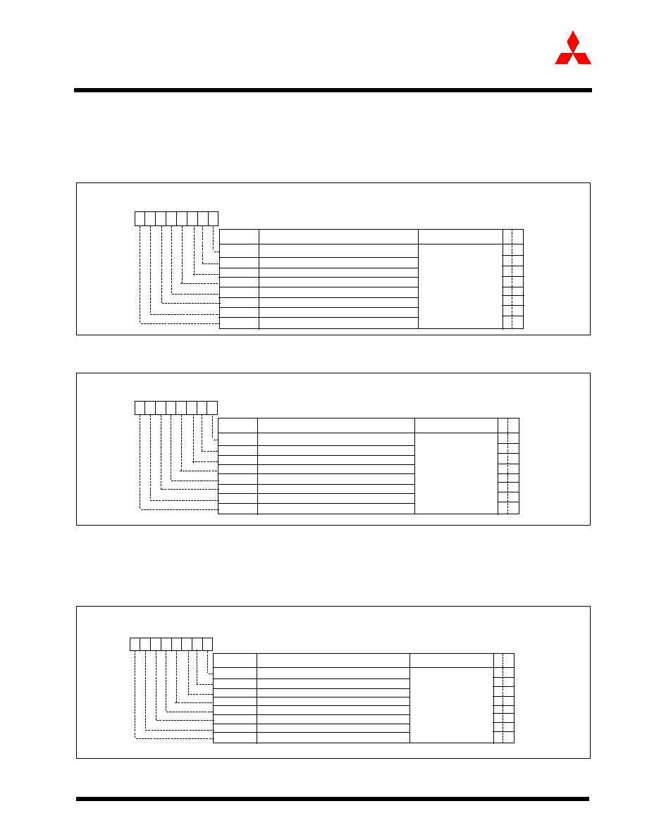
1-56
Mitsubishi microcomputers
M30240 Group
SINGLE-CHIP 16-BIT CMOS MICROCOMPUTER
Preliminary Specifications REV. E
Specifications in this manual are tentative and subject to change
Universal Serial Bus
2.18.4.10 USB DMAx Request Registers
The USB DMAx Request Registers, shown in Figure 1.41 and Figure 1.42, are used to select which USB End-
point x FIFO read/write requests are selected as the DMAC channel 0 or channel 1 request source. The USB
DMA0 (DMA1) Request Register should have only one bit set at any given time. When multiple bits are set,
no request is selected.
Figure 1.41:
USB DMA0 Request Register
Figure 1.42:
USB DMA1 Request Register
2.18.4.11 USB Endpoint Enable Register
The USB Endpoint Enable Register, shown in Figure 1.43, is used to enable/disable an individual endpoint.
Endpoint 0 is always enabled and cannot be disabled by firmware. All endpoints are enabled after reset.
Figure 1.43:
USB Endpoint Enable Register
USB DMA0 Request Register
Symbol
Address
When reset
USBSAR0
0309
16
00
16
Bit name
Bit symbol
b7
b6
b5
b4
b3
b2
b1
b0
Function
W
R
DMA0R0
DMA0R1
DMA0R2
DMA0R3
DMA0R4
DMA0R5
DMA0R6
DMA0R7
Endpoint 1 IN FIFO write request selection bit
Endpoint 2 IN FIFO write request selection bit
Endpoint 3 IN FIFO write request selection bit
Endpoint 4 IN FIFO write request selection bit
Endpoint 1 OUT FIFO read request selection bit
Endpoint 2 OUT FIFO read request selection bit
Endpoint 3 OUT FIFO read request selection bit
Endpoint 4 OUT FIFO read request selection bit
0 0
0 0
0 0
0 0
0 0
0 0
0 0
0 0
0 : Not selected
1 : Selected
USB DMA1 Request Register
Symbol
Address
When reset
USBSAR1
030A
16
00
16
Bit name
Bit symbol
b7
b6
b5
b4
b3
b2
b1
b0
Function
W
R
DMA1R0
DMA1R1
DMA1R2
DMA1R3
DMA1R4
DMA1R5
DMA1R6
DMA1R7
Endpoint 1 IN FIFO write request selection bit
Endpoint 2 IN FIFO write request selection bit
Endpoint 3 IN FIFO write request selection bit
Endpoint 4 IN FIFO write request selection bit
Endpoint 1 OUT FIFO read request selection bit
Endpoint 2 OUT FIFO read request selection bit
Endpoint 3 OUT FIFO read request selection bit
Endpoint 4 OUT FIFO read request selection bit
0 0
0 0
0 0
0 0
0 0
0 0
0 0
0 0
0 : Not selected
1 : Selected
USB Endpoint Enable Register
Symbol
Address
When reset
USBEPEN
030B
16
FF
16
Bit name
Bit symbol
b7
b6
b5
b4
b3
b2
b1
b0
Function
W
R
EP1_OUT
EP1_IN
EP2_OUT
EP2_IN
EP3_OUT
EP3_IN
EP4_OUT
EP4_IN
Endpoint 1OUT FIFO Enable bit
Endpoint 1 IN FIFO Enable bit
Endpoint 2OUT FIFO Enable bit
Endpoint 2 IN FIFO Enable bit
Endpoint 3 OUT FIFO Enable bit
Endpoint 3 IN FIFO Enable bit
Endpoint 4 OUT FIFO Enable bit
Endpoint 4 IN FIFO Enable bit
0 0
0 0
0 0
0 0
0 0
0 0
0 0
0 0
0 : Disabled
1 : Enabled

1-57
Mitsubishi microcomputers
M30240 Group
SINGLE-CHIP 16-BIT CMOS MICROCOMPUTER
Preliminary Specifications REV. E
Specifications in this manual are tentative and subject to change
Universal Serial Bus
2.18.4.12 Endpoint 0 CSR (Control and Status Register)
The Endpoint 0 CSR (Control and Status Register), shown in Figure 1.44 contains the control and status in-
formation of Endpoint 0.
�EP0CSR0 (OUT_PKT_RDY):
The USB FCU sets this bit to a "1" after it receives a valid SETUP/OUT token from the host. The CPU clears this
bit after unloading the packet from the FIFO by writing a "1" to EP0CSR6. The CPU should not clear the
OUT_PKT_RDY bit before it finishes decoding the host request. When EP0CSR2 (SEND_STALL) needs to be
set (because the CPU decodes an invalid or unsupported request) a "1" should be written to EP0CSR6 and
EP0CSR2 at the same time using the same instruction.
�
EP0CSR1 (IN_PKT_RDY):
The CPU writes a "1" to this bit after it finishes writing a packet of data to the endpoint 0 FIFO. The USB FCU
clears this bit after the packet is successfully transmitted to the host, or the EP0CSR5 (SETUP_END) bit is
set.
�
EP0CSR2 (SEND_STALL):
The CPU writes a "1" to this bit when it decodes an invalid or unsupported standard device request from the
host. When the OUT-PKT_RDY bit is a "1" at the time the CPU wants to set the SEND_STALL bit to a "1", the
CPU must also set SERVICED_OUT_PKT_RDY to a "1" to clear the OUT-PKT_RDY at the same time as set-
ting the SEND_STALL bit. The USB FCU returns a STALL handshake for all subsequent IN/OUT transactions
(during control transfer data or status stages) while this bit is set. The CPU writes a "0" to clear it after it re-
ceives a new SETUP packet. It is up to the firmware to decide what SETUP packet should lead the clearing
of the SEND_STALL bit.
�
EP0CSR3 (DATA_END):
The CPU writes a "1" to this bit when it writes (IN data phase) or reads (OUT data phase) the last packet of
data to or from the FIFO. The CPU sets this bit at the same time as it sets the last IN_PKT_RDY bit or sets
the last SERVICED_OUT_PKT_RDY bit.This bit indicates to the USB FCU that the specific amount of data in
the setup phase is transferred. The USB FCU advances to the status phase once this bit is set. When the
status phase completes, the USB FCU clears this bit. When this bit is set to a "1", and the host requests or
sends more data, the USB FCU returns a STALL handshake and terminates the current control transfer.
�
EP0CSR4 (FORCE_STALL):
The USB FCU sets this bit to a "1" to report an error status when one of the following occur:
� Host sends an IN token in the absence of a SETUP stage
� Host sends a bad data toggle in the STATUS stage, (i.e. DATA0 is used)
� Host sends a bad data toggle in the SETUP stage, (i.e. DATA1 is used)
� Host request more data than specified in the SETUP state,
(i.e. IN token comes after DATA_END bit is set)
� Host sends more data than specified in the SETUP state,
(i.e. OUT token comes after DATA_END bit is set)
� Host sends larger data packet than MAXP size
All of the conditions stated (except bad data toggle in the SETUP stage) cause the device to send a STALL
handshake for the current IN/OUT transaction. For the bad data toggle in the SETUP state, the device sends
ACK for the SETUP stage and then sends STALL for the next IN/OUT transaction. A STALL handshake
caused by the above listed conditions lasts for one transaction and terminates the ongoing control transfer.
Any packet after the STALL handshake will be seen as the beginning of a new control transfer.
The CPU writes a "0" to clear the FORCE_STALL status bit.
�
EP0CSR5 (SETUP_END):
The USB FCU sets this bit to a "1" if a control transfer has ended before the specific length of data is trans-
ferred during the data phase (status phase starts before DATA_END bit is set) or a control transfer has ended
before a new SETUP has arrived and before successfully completing the status phase. The CPU clears this
bit by writing a "1" to IN0CSR7. Once the CPU detects the SETUP_END bit as set, it should stop accessing
the FIFO to service the previous setup transaction. If the SETUP_END is caused by the reception of the SET-
UP packet prior to the end of the current control transfer, the OUT_PKT_RDY bit is set once the reception of
the SETUP packet has completed (without errors). After the OUT_PKT_RDY bit is set, the new SETUP packet
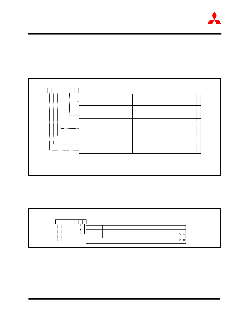
1-58
Mitsubishi microcomputers
M30240 Group
SINGLE-CHIP 16-BIT CMOS MICROCOMPUTER
Preliminary Specifications REV. E
Specifications in this manual are tentative and subject to change
Universal Serial Bus
data will be in the FIFO. For this case, because the SETUP_END bit is set near the beginning of the packet
when the SETUP PID is encountered and the OUT_PKT_RDY bit is set at the end of the packet, the value
read from EP0IN_CSR in the USB functional interrupt routine may only show that the SETUP_END bit as "1"
instead of both the SETUP_END and OUT_PKT_RDY bits.
�
EP0CSR6 and EP0CSR7:
These bits are used to clear EP0CSR0 and EP0CSR5 respectively. Writing a "1" to these bits clears the cor-
responding register bit.
Figure 1.44: USB Endpoint 0 CSR
2.18.4.13 USB Endpoint 0 MAXP Register
The USB Endpoint 0 MAXP Register, shown in Figure 1.45, indicates the maximum packet size (MAXP) of
Endpoint 0 IN/OUT packet. The default value for Endpoint 0 MAXP is 8 bytes.
Figure 1.45: USB Endpoint 0 MAXP
USB Endpoint 0 Control and Status Register (Note 5)
Symbol
Address
When reset
EP0CS
0311
16
00
16
Bit name
Bit symbol
b7
b6
b5
b4
b3
b2
b1
b0
Function
W
R
EP0CSR0
EP0CSR1
EPOCSR2
EPOCSR3
EP0CSR4
EPOCSR5
EP0CSR6
EPOCSR7
OUT_PKT_RDY Flag
IN_PKT_RDY Bit
SEND_STALL Bit
DATA_END Bit
FORCE_STALL Flag
SETUP_END Flag
SERVICED_OUT_PKY_RDY Bit
SERVICED_SETUP_END Bit
0 : Not ready
1 : Ready
0 : Not ready
1 : Ready
0 : No action
1 : Stall Endpoint 0 by CPU
0 : No action
1 : Last packet transferred from/to FIFO
0 : No action
1 : Stall Endpoint 0 by USB FCU
0 : No action
1 : Control transfer ended before specific
length of data transferred during data phase
0 : No change
1 : Clear the OUT_PKT_RDY bit (EPOCSR0)
0 : No change
1 : Clear the STUP-END bit (EP0CSR5)
0 0
0 0
0 0
0 0
0 0
0 0
0 0
0 0
Note 1: Read only
Note 2: Write "1" only or Read
Note 3: Write "0" only or Read
Note 4: Write only - Read "0"
Note 5: Refer to Section 5.5 "Programming Notes" for this register
Note 1
Note 1
Note 2
Note 3
Note 2
Note 4
Note 4
USB Endpoint 0 MAXP Register
Symbol
Address
When reset
EP0MP
0313
16
08
16
Bit name
Bit symbol
b7
b6
b5
b4
b3
b2
b1
b0
EP0MXP0 to
EP0MXP5
Function
W
R
Maximum packet size (MAXP)
of Endpoint 0 IN/OUT packet
Reserved
Must always be set to "0"
0 0
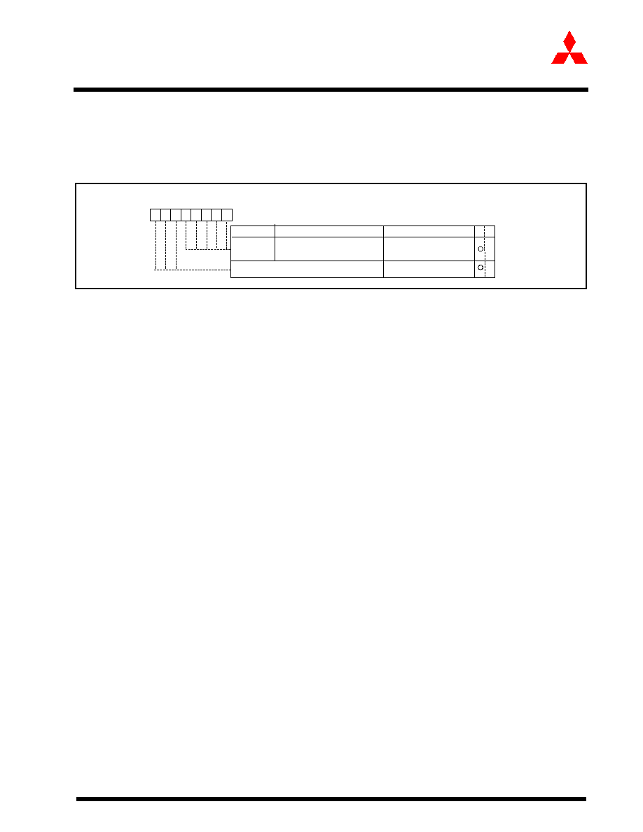
1-59
Mitsubishi microcomputers
M30240 Group
SINGLE-CHIP 16-BIT CMOS MICROCOMPUTER
Preliminary Specifications REV. E
Specifications in this manual are tentative and subject to change
Universal Serial Bus
2.18.4.14 USB Endpoint 0 OUT WRT CNT Register
The USB Endpoint 0 OUT WRT CNT Register, shown in Figure 1.46, contains the number of bytes of the cur-
rent data set in the OUT FIFO. The USB FCU sets the value in the Write Count Register after having success-
fully received a packet of data from the host. The CPU reads the register to determine the number of bytes to
be read from the FIFO.
Figure 1.46: USB Endpoint 0 OUT WRT CNT
2.18.4.15 USB Endpoint x IN CSR (Control & Status Register)
The USB Endpoint x IN CSR (Control and Status Register), shown in Figure 1.47, contains control and status
information of the respective IN endpoint 1-4.
�
INxCSR0 (IN_PKT_RDY) and INxCSR5 (TX_FIFO_NOT_EMPTY):
These two bits are for IN FIFO status when in read operation (see "IN (Transmit) FIFO" operation for details).
The CPU writes a "1" to the INxCSR0 bit to inform the USB FCU that a packet of data is written to the FIFO.
The USB FCU updates the pointers up on this bit set. The USB FCU also updates the pointers upon a packet
of data successfully sent to the host. When the pointer updates are completed, the IN FIFO status is shown
on INxCSR0 and INxCSR5 bits for the CPU to read. The CPU must allow at least one wait state between writ-
ing and reading these bits for proper FIFO status.
�
INxCSR1 (UNDER_RUN):
This bit is used in ISO mode only to indicate to the CPU that a FIFO underrun has occurred. The USB FCU
sets this bit to a "1" at the beginning of an IN token if no data packet is in the FIFO. Setting this bit causes the
INST12 bit of the Interrupt Status Register 2 to set. The CPU writes a "0" to clear this bit.
�
INxCSR2 (SEND_STALL):
The CPU writes a "1" to this bit when the endpoint is stalled (transmitter halt). The USB FCU returns a STALL
handshake while this bit is set. The CPU writes a "0" to clear this bit.
�
INxCSR3 (ISO/TOGGLE_INIT):
When the endpoint is used for isochronous data transfer, the CPU sets this bit to a "1" for the entire duration
of the isochronous transfer. With the ISO bit set to a "1", the device uses DATA0 as the pid for all packets sent
back to the host.
When the endpoint is required to initialize the data toggle, this set/reset of the TOGGLE_INIT bit method as-
sumes that there is no activity IN transaction to the respective endpoint on the bus at the time the initialization
process is ongoing. Set/reset of the TOGGLE_INIT bit is performed only when an endpoint experiences a con-
figuration event.
�
INxCSR4 (INTPT):
The CPU writes a "1" to this bit to initialize this endpoint as a status change endpoint for IN transactions. This
bit is set only when the corresponding endpoint is to be used to communicate rate feedback information (see
Chapter. IN (Transmit) FIFOs for details).
�
INxCSR5 (TX_FIFO_NOT_EMPTY):
The USB FCU sets this bit to a "1" when there is at least one data packet in the IN FIFO. This bit, in conjunction
with IN_PKT_RDY bit, provides the transmit IN FIFO status information (see "IN (Transmit) FIFO" for details).
�
INxCSR6 (FLUSH):
USB Endpoint 0 OUT Write Count Register
Symbol
Address
When reset
EP0WC
0315
16
00
16
Bit name
Bit symbol
b7
b6
b5
b4
b3
b2
b1
b0
W_CNT0 to
W_CNT4
Function
W
R
Receive byte count
Reserved
Must always be set to "0"
X
X
0 0 0
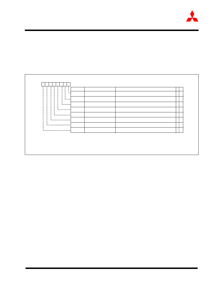
1-60
Mitsubishi microcomputers
M30240 Group
SINGLE-CHIP 16-BIT CMOS MICROCOMPUTER
Preliminary Specifications REV. E
Specifications in this manual are tentative and subject to change
Universal Serial Bus
The CPU writes a "1" to this bit to flush the IN FIFO. When there is one packet in the IN FIFO, a flush causes
the IN FIFO to be empty. When there are two packets in the IN FIFO, a flush causes the older packet to be
flushed out from the IN FIFO. Setting the INXCSR6 (FLUSH) bit during transmission could produce unpredict-
able results.
�INxCSR7 (AUTO_SET):
When the CPU sets this bit to a "1", the IN_PKT_RDY bit is set automatically by the USB FCU after the number
of bytes of data equal to the maximum packet size (MAXP) is written into the IN FIFO (see "IN (Transmit)
FIFO" operation for details).
Figure 1.47: USB Endpoint x IN CSR
2.18.4.16 USB Endpoint x OUT Control and Status Register
The USB Endpoint x OUT CSR (Control and Status Register), shown in Figure 1.48 contains control and sta-
tus information of the respective OUT endpoint 1-4.
�
OUTxCSR0 (OUT_PKT_RDY):
The OUTxCSR0 bit for the OUT FIFO status (see "OUT (Receive) FIFOs" for details).
The USB FCU sets this bit to a "1" and updates the FIFO pointers after a data packet has been successfully
received from the host. The CPU writes a "0" to this bit to inform the USB FCU that a data packet has been
unloaded. The USB FCU updates the FIFO pointers when this occurs. The CPU must allow at least one clock
cycle between writing and reading bit OUTxCSR0.
�
OUTXxCSR1 (OVER_RUN):
This bit is used in ISO mode only to indicate to the CPU that a FIFO overrun has occurred. The USB FCU sets
this bit to a "1" at the beginning of an OUT token when two data packets are already present in the FIFO. Set-
ting this bit causes the INST12 bit of the Interrupt Status Register 2 to set. The CPU writes a "0" to clear
OUTXCSR1.
�
OUTxCSR2 (SEND_STALL):
The CPU writes a "1" to this bit when the endpoint is stalled. The USB FCU returns a STALL handshake while
this bit is set. The CPU writes a "0" to clear this bit.
�
OUTxCSR3 (ISO/TOGGLE_INIT):
When the endpoint is used for isochronous data transfer, the CPU sets this bit to a "1" for the entire duration
of the isochronous transfer. With the ISO/TOGGLE_INIT bit set to a "1", the device accepts either DATA0 or
DATA1 for the PID sent by the host.
USB Endpoint x IN Control and Status Register (Note 5)
Symbol
Address
When reset
EPiICS (i= 1-4)
0319
16,
0321
16,
0329
16,
0331
16
00
16
Bit name
Bit symbol
b7
b6
b5
b4
b3
b2
b1
b0
Function
W
R
INxCSR0
INxCSR1
INxCSR2
INxCSR3
INxCSR4
INxCSR5
INxCSR6
INxCSR7
IN_PKT_RDY Bit
UNDER_RUN Flag
SEND_STALL Bit
ISO Bit
INTPT
TX_NOT_EPT Flag
FLUSH Bit
AUTO_SET Bit
0 : Not ready
1 : Ready
0 : No FIFO underrun
1 : FIFO underrun has occured
0 : No action
1 : Stall IN Endpoint x by CPU
0 : Select non-isochronous transfer
1 : Select isochronous transfer
0 : Select non-rate feedback interrupt transfer
1 : Select rate feedback interrupt transfer
0 : Transmit FIFO is empty
1 : Transmit FIFO is not empty
0 : No action
1 : Flush the FIFO
0 : AUTO-SET disabled
1 : AUTO-SET enabled
0 0
0 0
0 0
0 0
0 0
0 0
0 0
0 0
Note 1: Write "1" only or read
Note 2: Write "0" only or read
Note 3: Read only
Note 4: Write only - Read "0"
Note 5: Refer to section 5.5 "Programming Notes" for this register
Note 1
Note 2
Note 3
Note 4
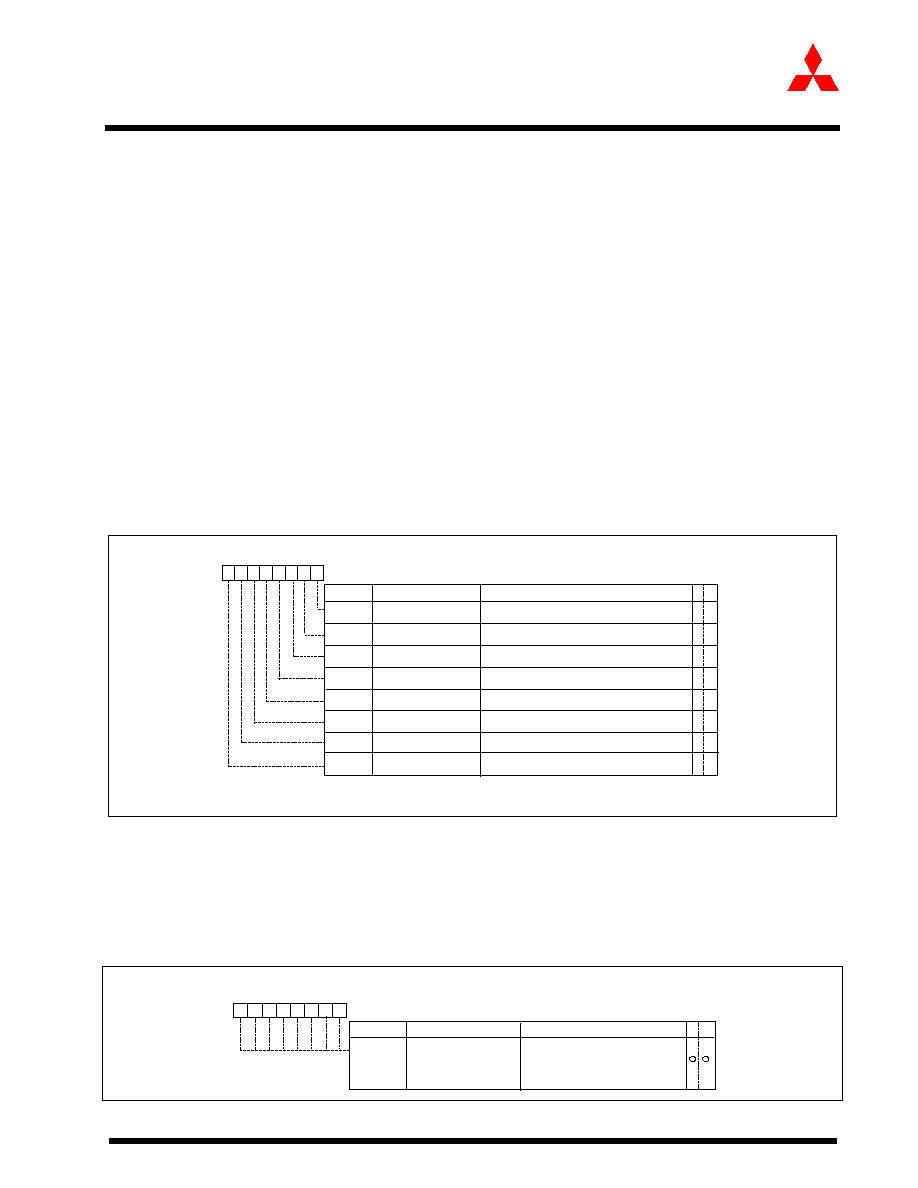
1-61
Mitsubishi microcomputers
M30240 Group
SINGLE-CHIP 16-BIT CMOS MICROCOMPUTER
Preliminary Specifications REV. E
Specifications in this manual are tentative and subject to change
Universal Serial Bus
When endpoint is required to initialize the data toggle sequence bit (i.e. reset to DATA0 for the next data pack-
et), the CPU sets this bit to a "1" and then resets it to a "0" to initialize the respective endpoint's data toggle.
Successful initialization of the data toggle sequence bit can only be guaranteed if no active OUT transaction
to the respective endpoint is ongoing when the initialization process is taking place. Set/reset of the ISO/
TOGGLE_INIT bit should only be performed when an endpoint experiences a configuration event.
�
OUTxCSR4 (FORCE_STALL):
The USB FCU sets this bit to a "1" when the host sends out a larger data packet than the MAXP size. The
USB FCU returns a STALL handshake while this bit is set. The CPU writes a "0" to clear this bit.
�
OUTxCSR5 (DATA_ERR):
The USB FCU sets this bit to a "1" to indicate that a CRC error or a bit stuffing error was received in an ISO
packet. The CPU writes a "0" to clear this bit.
�
OUTxCSR6 (FLUSH):
The CPU writes a "1" to this to flush the OUT FIFO. When there is one packet in the OUT FIFO, a flush causes
the OUT FIFO to be empty. When there are two packets in the OUT FIFO, a flush causes the older packet to
be flushed out from the OUT FIFO. Setting the OUTXCSR6 (FLUSH) bit during reception could produce un-
predictable results.
�
OUTxCSR7 (AUTO_CLR):
When the CPU sets this bit to a "1", the OUT_PKT_RDY bit is cleared automatically by the USB FCU after the
number of bytes of data equal to the maximum packet size (MAXP) is unloaded from the OUT FIFO (see "OUT
(Receive) FIFO" for details).
Figure 1.48: USB Endpoint x OUT CSR
2.18.4.17 USB Endpoint x IN MAXP Register
The USB Endpoint x IN MAXP Register, shown in Figure 1.49, indicates the maximum packet size (MAXP) of
an Endpoint x IN packet. The default values for Endpoints 1-4 are 0 bytes. The setting of this register also
affects the configuration of single/dual packet operation. When MAXP > 1/2 of the FIFO size, single packet
mode is set. When MAXP <= 1/2 of the FIFO size, dual packet mode is set.
Figure 1.49: USB Endpoint x IN MAXP
USB Endpoint x OUT Control and Status Register (Note 3)
Symbol
Address
When reset
EPiOCS (i = 1-4)
031A
16,
0322
16,
032A
16,
0332
16
00
16
Bit name
Bit symbol
b7
b6
b5
b4
b3
b2
b1
b0
Function
W
R
OUTxCSR0
OUTxCSR1
OUTxCSR2
OUTxCSR3
OUTxCSR4
OUTxCSR5
OUTxCSR6
OUTxCSR7
OUT_PKT_RDY Flag
OVER_RUN Flag
SEND_STALL Bit
ISO Bit
FORCE-STALL Flag
DATA-ERR Flag
FLUSH Bit
AUTO_CLR Bit
0 : Not ready
1 : Ready
0 : No FIFO overrun
1 : FIFO overrun occured
0 : No action
1 : Stall OUT Endpoint x by CPU
0 : Select non-isochronous transfer
1 : Select isochronous transfer
0 : No action
1 : Stall Endpoint X by the USB FCU
0 : No error
1 : CRC or bit stuffing error received in ISO packet
0 : No action
1 : Flush the FIFO
0 : AUTO-CLR disabled
1 : AUTO-CLR enabled
0 0
0 0
0 0
0 0
0 0
0 0
0 0
0 0
Note 1: Write "0" only or read
Note 2: Write only - Read "0"
Note 3: Refer to section 5.5 "Programming Notes" for this register
Note 1
Note 2
Note 1
Note 1
Note 1
USB Endpoint x IN MAXP Register
Symbol
Address
When reset
EPiIMP (i = 1-4) 031B
16,
0323
16,
032B
16,
0333
16
00
16
Bit name
Bit symbol
b7
b6
b5
b4
b3
b2
b1
b0
IMAXP0 to
IMAXP7
Function
W
R
Maximum packet size
(MAXP) of Endpoint x IN
packet.
For endpoints that support smaller
FIFO size, unused bits are not
implemented, (always write "0" to
those bits).

1-62
Mitsubishi microcomputers
M30240 Group
SINGLE-CHIP 16-BIT CMOS MICROCOMPUTER
Preliminary Specifications REV. E
Specifications in this manual are tentative and subject to change
Universal Serial Bus
2.18.4.18 USB Endpoint x OUT MAXP Register
The USB Endpoint x OUT MAXP Register, shown in Figure 1.50, indicates the maximum packet size (MAXP)
of an Endpoint x OUT packet. The default values for endpoints 1-4 are 0 bytes. The setting of this register also
affects the configuration of single/dual packet operation. When MAXP > 1/2 of the FIFO size, single packet is
set. When MAXP <= 1/2 of the FIFO size, dual packet mode is set.
Figure 1.50: USB Endpoint x OUT MAXP
2.18.4.19 USB Endpoint x OUT WRT CNT Register
The USB Endpoint x OUT WRT CNT Register, shown in Figure 1.51, contains the number of bytes of the cur-
rent data set in the OUT FIFO. The USB FCU sets the value in the Write Count Register after having success-
fully received a packet of data from the host. The CPU reads the register to determine the number of bytes to
be read from the FIFO.
Figure 1.51: USB Endpoint x OUT WRT CNT
2.18.4.20 USB Endpoint x FIFO Register
The USB Endpoint x FIFO Register, shown in Figure 1.52 is the USB IN (transmit) and OUT (receive) FIFO
data register. The CPU writes data to this register for the corresponding Endpoint IN FIFO and reads data from
this register for the corresponding Endpoint OUT FIFO.
Figure 1.52: USB Endpoint x FIFO Register
USB Endpoint x OUT MAXP Register
Symbol
Address
When reset
EPiOMP (i = 1-4) 031C
16,
0324
16,
032C
16,
0334
16
00
16
Bit name
Bit symbol
b7
b6
b5
b4
b3
b2
b1
b0
OMAXP0
to
OMAXP7
Function
W
R
Maximum packet size
(MAXP) of Endpoint x
OUT packet.
For endpoints that support smaller
FIFO size, unused bits are not
implemented, (always write "0" to
those bits).
USB Endpoint x OUT Write Count Register
Symbol
Address
When reset
EPiWC (i = 1-4) 031D
16,
0325
16,
032D
16,
0335
16
00
16
Bit name
Bit symbol
b7
b6
b5
b4
b3
b2
b1
b0
W_CNT0
to
W_CNT7
Function
W
R
Receive Byte Count
X
USB Endpoint x FIFO Register
Symbol
Address
When reset
EPi (i = 0-4) 0338
16,
0339
16,
033A
16,
033B
16,
033C
16
Indeterminate
Bit name
Bit symbol
b7
b6
b5
b4
b3
b2
b1
b0
DATA_0
to
DATA_7
Function
W
R
Endpoint x IN/OUT FIFO
register
X

1-63
Mitsubishi microcomputers
M30240 Group
SINGLE-CHIP 16-BIT CMOS MICROCOMPUTER
Preliminary Specifications REV. E
Specifications in this manual are tentative and subject to change
DMAC
2.19 DMAC
This microcomputer has two DMAC (direct memory access controller) channels that allow data to be
sent to memory without using the CPU.Table 1.14 shows the DMAC specifications. Figure 1.53 shows
the block diagram of the DMAC. Figure 1.54, Figure 1.55 and Figure 1.56 show the registers used by
the DMAC.
Table 1.14:
DMAC specifications
Item
Specification
Number of channels
2 (cycle steal method)
Transfer memory space
�From any SFR, RAM, or ROM address to a fixed address
�From a fixed address to any SFR or RAM address
�From a fixed address to a fixed address
(Note that DMA-related registers [0020
16
to 003F
16
] cannot be accessed)
Maximum number of bytes
transferred
128K bytes (with 16-bit transfers) or 64K bytes (with 8-bit transfers)
DMA request sources
Falling edge of INT0 or INT1 (INT0 can be selected by DMA0, INT1 by DMA1)
Timer A0 to timer A4
Timer B0 to timer B1
UART0 transmission and reception
UART1 transmission and reception
UART2 transmission and reception
A-D conversion complete
USB function
Software triggers
Channel priority
DMA0 takes precedence if DMA0 and DMA1 requests are generated simultaneously
Transfer unit
8 bits or 16 bits
Transfer address direction
forward/fixed (forward direction cannot be specified for both source and destination
simultaneously)
Transfer modes
Single transfer mode
The DMA enable bit is cleared and transfer ends when an underflow occurs in the
transfer counter.
Repeat transfer mode
When an underflow occurs in the transfer counter, the value in the transfer counter
reload register is loaded into the transfer counter and the DMA transfer is repeated
DMA interrupt request generation
timing
When an underflow occurs in the transfer counter
DMA startup
Single transfer mode
Transfer starts when the DMA is requested after "1" is written to the DMA enable bit
Repeat transfer mode
Transfer starts when the DMA is requested after "1" is written to the DMA enable bit
or after an underflow occurs in the transfer counter
DMA shutdown
When "0" is written to the DMA enable bit
When, in single transfer mode, an underflow occurs in the transfer counter
Forward address pointer and
reload timing for transfer counter
When DMA transfer starts, the value of whichever of the source or destination pointer that is set
up as the forward pointer is loaded into the forward address pointer. The value in the transfer
counter reload register is loaded into the transfer counter.
Writing to register
Registers specified for forward direction transfer are always write-enabled.
Registers specified for fixed address transfer are write-enabled when the DMA enable bit is "0".
Reading the register
Can be read at any time.
However, when the DMA enable bit is "1", reading the register sets up as the forward
register is the same as reading the value of the forward address pointer.

1-64
Mitsubishi microcomputers
M30240 Group
SINGLE-CHIP 16-BIT CMOS MICROCOMPUTER
Preliminary Specifications REV. E
Specifications in this manual are tentative and subject to change
DMAC
Figure 1.53: Block diagram of DMAC
Figure 1.54: DMAC register (1)
Data bus low-order bits
DMA latch high-order bits
DMA latch low-order bits
DMA0 source pointer SAR0(20)
DMA0 destination pointer DAR0 (20)
DMA0 forward address pointer (20)
Data bus high-order bits
Address bus
DMA1 destination pointer DAR1 (20)
DMA1 source pointer SAR1 (20)
DMA1 forward address pointer (20)
DMA0 transfer counter reload register TCR0 (16)
DMA0 transfer counter TCR0 (16)
DMA1 transfer counter reload register TCR1 (16)
DMA1 transfer counter TCR1 (16)
(addresses 0029
16
, 0028
16
)
(addresses 0039
16
, 0038
16
)
(addresses 0022
16
to 0020
16
)
(addresses 0026
16
to 0024
16
)
(addresses 0032
16
to 0030
16
)
(addresses 0036
16
to 0034
16
)
Note: Pointer is incremented by a DMA request.
DMAi request cause select register
Symbol
Address
When reset
DMiSL (i=0,1)
03B8
16,
03BA
16
00
16
Function
Bit symbol
b7
b6
b5
b4
b3
b2
b1
b0
DMA request cause
select bit
DSEL0
R
W
DSEL1
DSEL2
DSEL3
Nothing is assigned.
These bits can neither be set nor reset. When read, the value of these bits is "0".
Software DMA
request bit
If software trigger is selected, a
DMA request is generated by
setting this bit to "1" (When read,
the value of this bit is always "0")
DSR
b3 b2 b1 b0
0 0 0 0 : Falling edge of INT0 / INT1 pin
(Note1)
0 0 0 1 : Software trigger
0 0 1 0 : Timer A0
0 0 1 1 : Timer A1
0 1 0 0 : Timer A2
0 1 0 1 : Timer A3
0 1 1 0 : Timer A4
0 1 1 1 : Timer B0
1 0 0 0 : Timer B1
1 0 0 1 : USB0/USB1 (Note 3)
1 0 1 0 : UART0 transmit
1 0 1 1 : UART0 receive
1 1 0 0 : UART2 transmit
1 1 0 1 : UART2 receive
1 1 1 0 : A-D conversion
1 1 1 1 : UART1 transmit / UART1 receive
(Note 2)
Bit name
Note 1: Address 03B8
16
is for INT0, 03BA
16
is for INT1.
Note 2: Address 03B8
16
is for UART1 transmit, 03BA
16
is for UART1 receive.
Note 3: Address 03B8
16
is for USB0, 03BA
16
is for USB1.
1-65
Mitsubishi microcomputers
M30240 Group
SINGLE-CHIP 16-BIT CMOS MICROCOMPUTER
Preliminary Specifications REV. E
Specifications in this manual are tentative and subject to change
DMAC
Figure 1.55: DMAC register (2)
Figure 1.56: DMAC register (3)
DMAi control register
Symbol
Address
When reset
DMiCON(i=0,1)
002C
16
, 003C
16
00000X00
2
Bit name
Function
Bit symbol
Transfer unit bit select bit
b7
b6
b5
b4
b3
b2
b1
b0
0 : 16 bits
1 : 8 bits
DMBIT
R
W
DMASL
DMAS
DMAE
Repeat transfer mode
select bit
0 : Single transfer
1 : Repeat transfer
DMA request bit (Note 1)
0 : DMA not requested
1 : DMA requested
0 : Disabled
1 : Enabled
0 : Fixed
1 : Forward
DMA enable bit
Source address direction
select bit (Note 3)
Destination address
direction select bit (Note 3)
0 : Fixed
1 : Forward
DSD
DAD
Nothing is assigned.
These bits can neither be set nor reset. When read, the value of these bits is "0".
Note 1: DMA request can be cleared by resetting the bit.
Note 2: This bit can only be set to "0".
Note 3: Source address direction select bit and destination address direction select bit
cannot be set to "1" simultaneously.
(Note 2)
b7
b0
b7
b0
(b8)
(b15)
Function
R W
Transfer counter
Set a value one less than the transfer count
Symbol
Address
When reset
TCR0
0029
16
, 0028
16
Indeterminate
TCR1
0039
16
, 0038
16
Indeterminate
DMAi transfer counter (i = 0, 1)
Transfer count
specification
0000
16
to FFFF
16
b7
(b23)
b3
b0
b7
b0
b7
b0
(b8)
(b16)(b15)
(b19)
Function
R W
Source pointer
Stores the source address
Symbol
Address
When reset
SAR0
0022
16
to 0020
16
Indeterminate
SAR1
0032
16
to 0030
16
Indeterminate
DMAi source pointer (i = 0, 1)
Transfer count
specification
00000
16
to FFFFF
16
Nothing is assigned.
These bits can neither be set nor reset. When read, the value of these bits is "0".
Symbol
Address
When reset
DAR0
0026
16
to 0024
16
Indeterminate
DAR1
0036
16
to 0034
16
Indeterminate
b3
b0
b7
b0
b7
b0
(b8)
(b15)
(b16)
(b19)
Function
R W
Destination pointer
Stores the destination address
DMAi destination pointer (i = 0, 1)
Transfer count
specification
00000
16
to FFFFF
16
b7
(b23)
Nothing is assigned.
These bits can neither be set nor reset. When read, the value of these bits is "0".
1-66
Mitsubishi microcomputers
M30240 Group
SINGLE-CHIP 16-BIT CMOS MICROCOMPUTER
Preliminary Specifications REV. E
Specifications in this manual are tentative and subject to change
DMAC
2.19.1 Transfer cycle
The transfer cycle consists of the bus cycle in which data is read from memory or from the SFR area
(source read) and the bus cycle in which the data is written to memory or to the SFR area (destination
write). The number of read and write bus cycles depends on the source and destination addresses
and the software waits are inserted.
2.19.1.1 Effect of source and destination addresses
When 16-bit data is transferred on a 16-bit data bus, and the source and destination both start at odd address-
es, there is one more source read cycle and destination write cycle than when the source and destination both
start at even addresses.
2.19.2 DMAC transfer cycles
Any combination of even or odd transfer read and write addresses is possible. Table 1.15 show the
number of DMAC transfer cycles. Table 1.16 shows the corresponding coefficient values. Figure 1.57
shows an example of the transfer cycle for a source read.
The number of DMAC transfer cycles can be calculated as follows:
Number of transfer cycles per transfer unit = Number of read cycles x j + Number of write cycles x k
Table 1.15:
Number of DMAC transfer cycles
Transfer unit
Access
address
Single-chip mode
Number of
read cycles
Number of
write cycles
8-bit transfers
(DMBIT="1")
Even
1
1
Odd
1
1
16-bit transfers
(DMBIT="0")
Even
1
1
Odd
2
2
Table 1.16:
Coefficients j,k
Internal memory
Internal ROM/
RAM No wait
Internal ROM/
RAM with wait
SFR area
1
2
2
1-67
Mitsubishi microcomputers
M30240 Group
SINGLE-CHIP 16-BIT CMOS MICROCOMPUTER
Preliminary Specifications REV. E
Specifications in this manual are tentative and subject to change
DMAC
Figure 1.57: Example of the transfer cycle for a source read
CLKout
Address
bus
Data
bus
CPU use
CPU use
CPU use
CPU use
Source
Source
Destination
Destination
Dummy
cycle
Dummy
cycle
(1) 8-bit transfers
16-bit transfers from even address and the source address is even.
CLKout
Address
bus
RD signal
WR signal
Data
bus
CPU use
CPU use
CPU use
CPU use
Source
Source
Destination
Destination
Dummy
cycle
Dummy
cycle
(3) One wait is inserted into the source read under the conditions in (1)
CLKout
Address
bus
Data
bus
CPU use
CPU use
CPU use
CPU use
Source
Source
Destination
Destination
Dummy
cycle
Dummy
cycle
Source + 1
Source + 1
(2) 16-bit transfers and the source address is odd
Transferring 16-bit data on an 8-bit data bus (In this case, there are two destination write cycles).
CLKout
Address
bus
RD signal
WR signal
Data
bus
CPU use
CPU use
CPU use
CPU use
Source
Source
Destination
Destination
Dummy
cycle
Dummy
cycle
Source + 1
Source + 1
(4) One wait is inserted into the source read under the conditions in (2)
(When 16-bit data is transferred on an 8-bit data bus, there are two destination write cycles).
Note: The same timing changes occur with the respective conditions at the destination as at the source.

1-68
Mitsubishi microcomputers
M30240 Group
SINGLE-CHIP 16-BIT CMOS MICROCOMPUTER
Preliminary Specifications REV. E
Specifications in this manual are tentative and subject to change
Timers
2.20 Timers
There are eight 16-bit timers. These timers can be classified by function into timers A (five) and timers
B (three). All these timers function independently. Figure 1.58 shows the block diagram of Timers A and
B.
Figure 1.58: Timer A and Timer B block diagram
Timer A3 interrupt
Timer A4 interrupt
Timer A1 interrupt
Timer A2 interrupt
Timer A0 interrupt
Timer B1 interrupt
� Timer mode
� One-shot mode
� PWM mode
� Timer mode
� One-shot mode
� PWM mode
� Timer mode
� One-shot mode
� PWM mode
� Timer mode
� One-shot mode
� PWM mode
� Timer mode
� One-shot mode
� PWM mode
� Event counter mode
� Event counter mode
� Event counter mode
� Event counter mode
� Event counter mode
TA0
IN
TA1
IN
TA2
IN
TA3
IN
TA4
IN
Timer A0
Timer A1
Timer A2
Timer A3
Timer A4
f
1
f
8
f
32
Noise
filter
Noise
filter
Noise
filter
Noise
filter
Noise
filter
1/8
1/4
f
1
f
8
f
32
X
IN
Timer B0 interrupt
� Timer mode
� Timer mode
� Timer mode
Timer B0
Timer B1
Timer B2
Timer B2
interrupt
1-69
Mitsubishi microcomputers
M30240 Group
SINGLE-CHIP 16-BIT CMOS MICROCOMPUTER
Preliminary Specifications REV. E
Specifications in this manual are tentative and subject to change
Timer A
2.21 Timer A
Figure 1.59, Figure 1.60,Figure 1.61, and Figure 1.62 show the timer A-related registers.
Except in event counter mode, timers A0 through A4 all have the same function. Use the timer Ai mode
register (i = 0 to 4) bits 0 and 1 to choose the desired mode.
Timer A has the four operation modes listed as follows:
� Timer mode: The timer counts an internal count source.
� Event counter mode: The timer counts pulses from an external source or a timer over flow.
� One-shot timer mode: The timer stops counting when the count reaches "0000
16
".
� Pulse width modulation (PWM) mode: The timer outputs pulses of a given width.
Figure 1.59: Block diagram of Timer A
Figure 1.60: Timer A related Registers (1)
TAi
Addresses
TAj
TAk
Timer A0 0387
16
0386
16
Timer A4 Timer A1
Timer A1 0389
16
0388
16
Timer A0 Timer A2
Timer A2 038B
16
038A
16
Timer A1 Timer A3
Timer A3 038D
16
038C
16
Timer A2 Timer A4
Timer A4 038F
16
038E
16
Timer A3 Timer A0
Count start flag
(Address 0380
16
)
Up count/down count
Always down count except
in event counter mode
Reload register (16)
Counter (16)
Low-order
8 bits
High-order
8 bits
Clock source
selection
� Timer
(gate function)
� Timer
� One shot
� PWM
f
1
f
8
f
32
External
trigger
TAi
IN
(i = 0 to 4)
TB2 overflow
� Event counter
Clock selection
TAj overflow
(j = i � 1. Note, however, that j = 4 when i = 0)
Pulse output
Toggle flip-flop
TAi
OUT
(i = 0 to 4)
Data bus low-order bits
Data bus high-order bits
Up/down flag
Down count
(Address 0384
16
)
TAk overflow
(k = i + 1. Note, however, that k = 0 when i = 4)
Polarity
selection
Timer Ai mode register
Symbol
Address
When reset
TAiMR(i=0 to 4)
0396
16
to 039A
16
00
16
Bit name
Function
Bit symbol
W
R
b7
b6
b5
b4
b3
b2
b1
b0
Operation mode
select bit
0 0 : Timer mode
0 1 : Event counter mode
1 0 : One-shot timer mode
1 1 : Pulse width modulation (PWM) mode
b1 b0
TMOD1
TMOD0
MR0
MR2
MR1
MR3
TCK1
TCK0
Count source select bit
Function varies with each operation mode
Function varies with each operation mode
1-70
Mitsubishi microcomputers
M30240 Group
SINGLE-CHIP 16-BIT CMOS MICROCOMPUTER
Preliminary Specifications REV. E
Specifications in this manual are tentative and subject to change
Timer A
Figure 1.61: Timer A-related registers (2)
Timer A4 up/down flag
Timer A3 up/down flag
Timer A2 up/down flag
Timer A1 up/down flag
Timer A0 up/down flag
Timer A2 two-phase pulse
signal processing select bit
Timer A3 two-phase pulse
signal processing select bit
Timer A4 two-phase pulse
signal processing select bit
Symbol
Address
When reset
UDF
0384
16
00
16
TA4P
TA3P
TA2P
Up/down flag
Bit name
Function
Bit symbol
W
R
b7
b6
b5
b4
b3
b2
b1
b0
TA4UD
TA3UD
TA2UD
TA1UD
TA0UD
0 : Down count
1 : Up count
This specification becomes valid
when the up/down flag content is
selected for up/down switching
cause
0 : two-phase pulse signal
processing disabled
1 : two-phase pulse signal
processing enabled
When not using the two-phase
pulse signal processing function,
set the select bit to "0"
Symbol
Address
When reset
TABSR
0380
16
00
16
Count start flag
Bit name
Function
Bit symbol
W
R
b7
b6
b5
b4
b3
b2
b1
b0
Timer B2 count start flag
Timer B1 count start flag
Timer B0 count start flag
Timer A4 count start flag
Timer A3 count start flag
Timer A2 count start flag
Timer A1 count start flag
Timer A0 count start flag
0 : Stops counting
1 : Starts counting
TB2S
TB1S
TB0S
TA4S
TA3S
TA2S
TA1S
TA0S
Symbol
Address
When reset
TA0
0387
16
,0386
16
Indeterminate
TA1
0389
16
,0388
16
Indeterminate
TA2
038B
16
,038A
16
Indeterminate
TA3
038D
16
,038C
16
Indeterminate
TA4
038F
16
,038E
16
Indeterminate
b7
b0 b7
b0
(b15)
(b8)
Timer Ai register (Note)
W
R
Timer mode
0000
16
to FFFF
16
Counts an internal count source
Function
Values that can be set
Event counter mode
0000
16
to FFFF
16
Counts pulses from an external source or timer overflow
One-shot timer mode
0000
16
to FFFF
16
Counts a one shot width
Pulse width modulation mode (16-bit PWM)
Functions as a 16-bit pulse width modulator
Pulse width modulation mode (8-bit PWM)
Timer low-order address functions as an 8-bit
prescaler and high-order address functions as an 8-bit
pulse width modulator
00
16
to FE
16
(Both high-order
and low-order
addresses)
0000
16
to FFFE
16
Note: Read and write data in 16-bit units.
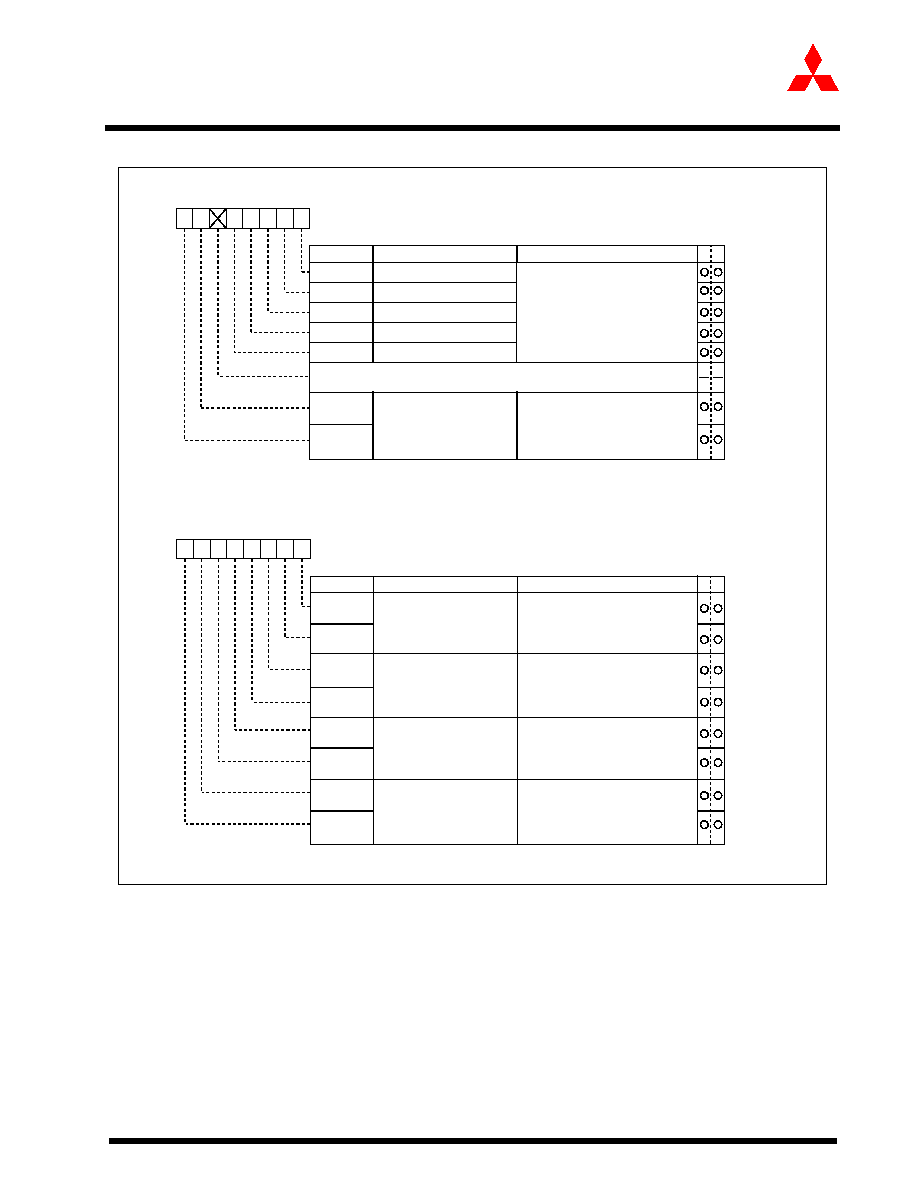
1-71
Mitsubishi microcomputers
M30240 Group
SINGLE-CHIP 16-BIT CMOS MICROCOMPUTER
Preliminary Specifications REV. E
Specifications in this manual are tentative and subject to change
Timer A
Figure 1.62: Timer A-related registers (3)
TA1TGL
Symbol
Address
When reset
TRGSR
0383
16
00
16
Timer A1 event/trigger
select bit
0 0 :
Input on TA1
IN
is selected (Note)
0 1 : TB2 overflow is selected
1 0 : TA0 overflow is selected
1 1 : TA2 overflow is selected
Trigger select register
Bit name
Function
Bit symbol
b7
b6
b5
b4
b3
b2
b1
b0
0 0 :
Input on TA2
IN
is selected (Note)
0 1 : TB2 overflow is selected
1 0 : TA1 overflow is selected
1 1 : TA3 overflow is selected
0 0 :
Input on TA3
IN
is selected (Note)
0 1 : TB2 overflow is selected
1 0 : TA2 overflow is selected
1 1 : TA4 overflow is selected
0 0 :
Input on TA4
IN
is selected (Note)
0 1 : TB2 overflow is selected
1 0 : TA3 overflow is selected
1 1 : TA0 overflow is selected
Timer A2 event/trigger
select bit
Timer A3 event/trigger
select bit
Timer A4 event/trigger
select bit
W
R
TA1TGH
TA2TGL
TA2TGH
TA3TGL
TA3TGH
TA4TGL
TA4TGH
b1 b0
b3 b2
b5 b4
b7 b6
Note: Set the corresponding port direction register to 0 .
TA1OS
TA2OS
TA0OS
One-shot start flag
Symbol
Address
When reset
ONSF
0382
16
00X00000
2
Timer A0 one-shot start flag
Timer A1 one-shot start flag
Timer A2 one-shot start flag
Timer A3 one-shot start flag
Timer A4 one-shot start flag
TA3OS
TA4OS
Bit name
Function
Bit symbol
b7
b6
b5
b4
b3
b2
b1
b0
Nothing is assigned.
This bit can neither be set nor reset. When read, its content is indeterminate.
TA0TGL
TA0TGH
0 0 :
Input on TA0
IN
is selected (Note)
0 1 : TB2 overflow is selected
1 0 : TA4 overflow is selected
1 1 : TA1 overflow is selected
Timer A0 event/trigger
select bit
b7 b6
Note: Set the corresponding port direction register to 0 .
W
R
1 : Timer start
When read, the value is 0

1-72
Mitsubishi microcomputers
M30240 Group
SINGLE-CHIP 16-BIT CMOS MICROCOMPUTER
Preliminary Specifications REV. E
Specifications in this manual are tentative and subject to change
Timer A
2.21.1 Timer mode
In this mode, the timer counts an internally generated count source. See Table 1.17 below. Figure
1.63 shows the timer Ai mode register in timer mode.
Figure 1.63: Timer Ai mode register in timer mode
Table 1.17:
Specifications of timer mode
Item
Specification
Count source
f1, f8, f32
Count operation
� Down count
� When the timer underflows, it loads the reload register contents before continuing counting
Divide ratio
1/(n+1) n: Set value
Count start condition
Count start flag is set (= 1)
Count stop condition
Count start flag is reset (= 0)
Interrupt request
generation timing
When the timer underflows
TAiIN pin function
Programmable I/O port or gate input
TAiOUT pin function
Programmable I/O port or pulse output
Read from timer
Count value can be read out by reading timer Ai register
Write to timer
� When counting is stopped and a value is written to timer Ai register, it is written to both reload register and counter
� When counting is in progress and a value is written to timer Ai register, it is written only to reload register (to be
transferred to counter at the next reload time)
Select function
� Gate function
Counting can be started and stopped by TAiIN pin's input signal
� Pulse output function
Each time the timer underflows, the TAiOUT pin's polarity is reversed
Note 1: The settings of the corresponding port register and port direction register
are invalid.
Note 2: The bit can be "0" or "1".
Note 3: Set the corresponding port direction register to "0".
Timer Ai mode register
Symbol
Address
When reset
TAiMR(i=0 to 4)
0396
16
to 039A
16
00
16
Bit name
Function
Bit symbol
W
R
b7
b6
b5
b4
b3
b2
b1
b0
Operation mode
select bit
0 0 : Timer mode
b1 b0
TMOD1
TMOD0
MR0
Pulse output function
select bit
0 : Pulse is not output
(TA
iOUT
pin is a normal port pin)
1 : Pulse is output (Note 1)
(TA
iOUT
pin is a pulse output pin)
Gate function select bit
0 X
(Note 2)
: Gate function not available
(TAi
IN
pin is a normal port pin)
1 0 : Timer counts only when TA
iIN
pin is
held "L" (Note 3)
1 1 : Timer counts only when TA
iIN
pin is
held "H" (Note 3)
b4 b3
MR2
MR1
MR3
0 (Must always be fixed to "0" in timer mode)
0 0 : f
1
0 1 : f
8
1 0 : f
32
1 1 : Reserved
b7 b6
TCK1
TCK0
Count source select bit
0
0
0

1-73
Mitsubishi microcomputers
M30240 Group
SINGLE-CHIP 16-BIT CMOS MICROCOMPUTER
Preliminary Specifications REV. E
Specifications in this manual are tentative and subject to change
Timer A
2.21.2 Event counter mode
In this mode, the timer counts an external signal or an internal timer's overflow. Timers A0 and A1 can
count a single-phase external signal. Timers A2, A3, and A4 can count a single-phase and a two-phase
external signal. Table 1.18 lists the timer specifications when counting a single-phase external signal.
Figure 1.64 shows Timer Ai mode register in event counter mode, single-phase signal.
Table 1.18:
Timer specification in event counter mode (when not processing two-phase pulse signal)
Item
Specification
Count source
�External signals input to TAiIN pin (effective edge can be selected by software
�TB2 overflow, TAj overflow
Count operation
�Up count or down count can be selected by external signal or software
�When the timer overflows or underflows, it loads from the reload register contents before
continuing counting. (However, this does not apply when the free-run function is selected.)
Divide ratio
1/ (FFFF
16
- n+1) for up count
1/ (n + 1) for down count n: set value
Count start condition
Count start flag is set (=1)
Count stop condition
Count start flag is reset (=0)
Interrupt request
generation timing
Timer overflows or underflows
TAiIN pin function
Programmable I/O port or count source input
TAiOUT pin function
Programmable I/O port, pulse output, or up/down count select input
Read from timer
Count value can be read out by reading timer Ai register
Write to timer
�When counting is stopped and a value is written to timer Ai register, it is written to both
reload register and counter
�When counting is in progress and a value is written to timer Ai register, it is written to only
reload register
Select function
�Free-run count function
When the timer overflows or underflows, the reload register content is not reloaded.
�Pulse output function
Each time the timer overflows, the TAiOUT pin`s polarity is reversed
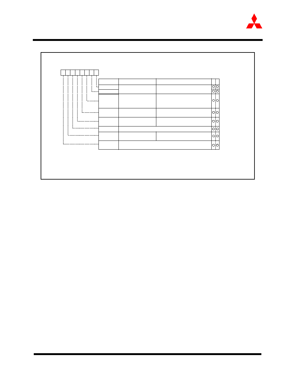
1-74
Mitsubishi microcomputers
M30240 Group
SINGLE-CHIP 16-BIT CMOS MICROCOMPUTER
Preliminary Specifications REV. E
Specifications in this manual are tentative and subject to change
Timer A
Figure 1.64: Timer Ai mode register in event counter mode, single signal
Table 1.19 shows the Timer specification in event counter mode when processing two-phase signal with timers
A2, A3, and A4.
Figure 1.65 shows Timer Ai mode register in event counter mode when processing two-phase signal.
Note 1: In event counter mode, the count source is selected by the event / trigger select bit
(addresses 0382
16
and 0383
16
).
Note 2: The settings of the corresponding port register and port direction register are invalid.
Note 3: Valid only when counting an external signal.
Note 4: When an "L" signal is input to the TAi
OUT
pin, the downcount is activated. When "H",
the upcount is activated. Set the corresponding port direction register to "0".
Note 5: This value can be indeterminate when the count starts.
Timer Ai mode register
Symbol
Address
When reset
TAiMR(i = 0, 1)
0396
16
, 0397
16
00
16
W
R
b7
b6
b5
b4
b3
b2
b1
b0
Operation mode select bit
0 1 : Event counter mode
(Note 1)
b1 b0
TMOD0
MR0
Pulse output function
select bit
0 : Pulse is not output
(TA
iOUT
pin is a normal port pin)
1 : Pulse is output (Note 2)
(TA
iOUT
pin is a pulse output pin)
Count polarity
select bit (Note 3)
MR2
MR1
MR3
0 (Must always be fixed to "0" in event counter mode)
TCK0
Count operation type
select bit
0 1
0
0 : Counts external signal's falling edge
1 : Counts external signal's rising edge
Up/down switching
cause select bit
0 : Up/down flag's content
1 : TA
iOUT
pin's input signal (Note 4)
0 : Reload type
1 : Free-run type (Note 5)
Bit symbol
Bit name
Function
R W
TCK1
Invalid in event counter mode
Can be "0" or "1"
TMOD1

1-75
Mitsubishi microcomputers
M30240 Group
SINGLE-CHIP 16-BIT CMOS MICROCOMPUTER
Preliminary Specifications REV. E
Specifications in this manual are tentative and subject to change
Timer A
Table 1.19:
Timer specification in even counter mode (when processing two-phase pulse signal with
timers A2, A3, and A4)
Item
Specification
Count Source
�Two-phase pulse signals input to TAiIN or TAiOUT pin
Count operation
�Up count or down count can be selected by two-phase pulse signal
�When the timer overflows or underflows, the reload register content is loaded and the timer
starts over again (Note 1)
Divide ratio
1/ (FFFF
16
- n + 1) for up count
1/ (n+1) for down count n: Set value
Count start condition
Count start flag is set (=1)
Count stop condition
Count start flag is reset (=0)
Interrupt request
generation timing
Timer overflow or underflows
TAi
IN
pin function
Two-phase pulse input
TAi
OUT
pin function
Two-phase pulse input
Read from timer
Count value can be read out by reading timer A2, A3, or A4 register
Writer to timer
�When counting is stopped and a value is written to timer A2, A3, or A4 register, it is written
to both the reload register and counter
�When counting is in progress and a value is written to timer A2, A3, or A4 register, it is
written to only reload register to be transferred to counter at the next reload time.
Select function
�Normal processing operation
The timer counts up rising edges or counts down falling edges on the TAi
IN
pin when input
signal on the TAi
OUT
pin is "H"
�Multiply-by-4 processing operation
If the phase relationship is such that the
TAi
IN
pin goes "H" when the input signal on the
TAi
OUT
pin is "H", the timer counts up rising and falling edges on the
TAi
OUT a
nd T
Ai
IN
pins.
If the phase relationship is such that the T
Ai
IN
pin goes "L" when the input signal on the
TAi
OUT
pin is "H", the timer counts down rising and falling edges on the
TAi
OUT
and T
Ai
IN
pins.
Note 1
This does not apply when the free-run function is selected.
TAi
OUT
TAi
IN
(i=2,3)
Up
count
Up
count
Up
count
Down
count
Down
count
Down
count
Count up all edges
Count down all edges
Count down all edges
Count up all edges
TAi
OUT
T
Ai
IN
(i=3,4)

1-76
Mitsubishi microcomputers
M30240 Group
SINGLE-CHIP 16-BIT CMOS MICROCOMPUTER
Preliminary Specifications REV. E
Specifications in this manual are tentative and subject to change
Timer A
Figure 1.65: Timer Ai mode register in event counter mode, two-phase signal
Note 1: The settings of the corresponding port register and port direction register are invalid.
Note 2: This bit is valid when only counting an external signal.
Note 3: Set the corresponding port direction register to "0".
Note 4: This bit is valid for the timer A3 mode register.
For timer A2 and A4 mode registers, this bit can be "0 "or "1".
Note 5: When performing two-phase pulse signal processing, make sure the two-phase pulse
signal processing operation select bit (address 0384
16
) is set to "1". Also, always be
sure to set the event/trigger select bit (addresses 0382
16
and 0383
16
) to "00".
Note 6: This value can be indeterminate when the count starts.
Timer Ai mode register
(When not using two-phase pulse signal processing)
Symbol
Address
When reset
TAiMR(i = 2 to 4) 0398
16
to 039A
16
00
16
b7
b6
b5
b4
b3
b2
b1
b0
Operation mode select bit
0 1 : Event counter mode
b1 b0
TMOD1
TMOD0
MR0
Pulse output function
select bit
0 : Pulse is not output
(TAi
OUT
pin is a normal port pin)
1 : Pulse is output (Note 1)
(TAi
OUT
pin is a pulse output pin)
Count polarity
select bit (Note 2)
MR2
MR1
MR3
0 : (Must always be "0" in event counter mode)
TCK1
TCK0
0 1
0
0 : Counts external signal's falling edges
1 : Counts external signal's rising edges
Up/down switching
cause select bit
0 : Up/down flag's content
1 : TA
iOUT
pin's input signal (Note 3)
Bit symbol
Bit name
Function
W
R
Count operation type
select bit
Two-phase pulse signal
processing operation
select bit (Note 4)(Note 5)
0 : Reload type
1 : Free-run type (Note 6)
0 : Normal processing operation
1 : Multiply-by-4 processing operation
Note 1: This bit is valid for timer A3 mode register.
For timer A2 and A4 mode registers, this bit can be "0" or "1".
Note 2: When performing two-phase pulse signal processing, make sure the two-phase pulse
signal processing operation select bit (address 0384
16
) is set to "1". Also, always be
sure to set the event/trigger select bit (addresses 0382
16
and 0383
16
) to "00".
Note 3: This value can be indeterminate when the count starts.
Timer Ai mode register
(When using two-phase pulse signal processing)
Symbol
Address
When reset
TAiMR(i = 2 to 4) 0398
16
to 039A
16
00
16
b7
b6
b5
b4
b3
b2
b1
b0
Operation mode select bit
0 1 : Event counter mode
b1 b0
TMOD1
TMOD0
MR0
0 (Must always be "0" when using two-phase pulse signal
processing)
0 (Must always be "0" when using two-phase pulse signal
processing)
MR2
MR1
MR3
0 (Must always be "0" when using two-phase pulse signal
processing)
TCK1
TCK0
0 1
0
1 (Must always be "1" when using two-phase pulse signal
processing)
Bit symbol
Bit name
Function
W
R
Count operation type
select bit
Two-phase pulse
processing operation
select bit (Note 1)(Note 2)
0 : Reload type
1 : Free-run type (Note 3)
0 : Normal processing operation
1 : Multiply-by-4 processing operation
0
0
1

1-77
Mitsubishi microcomputers
M30240 Group
SINGLE-CHIP 16-BIT CMOS MICROCOMPUTER
Preliminary Specifications REV. E
Specifications in this manual are tentative and subject to change
Timer A
2.21.3 One-shot timer mode
In this mode, the timer operates only once (See Table 1.20 ). When a trigger occurs, the timer starts
up and continues operating for a given period. Figure 1.66 shows the timer Ai mode register in one-
shot mode.
Figure 1.66: Timer Ai mode register in one-shot mode
Table 1.20:
Timer specifications in one-shot timer mode
Item
Specification
Count source
f1, f8, f32
Count operation
�The timer counts down
�When the count reaches 0000
16
, the timer stops counting after reloading a new count
� If a trigger occurs when counting, the timer reloads a new count and restarts counting
Divide ratio
1/n n: Set value
Count start condition
� An external trigger is input
� The selected timer overflows
� The one-shot start flag is set (= 1)
Count stop condition
� A new count is reloaded after the count has reached 0000
16
� The count start flag is reset (= 0)
Interrupt request
generation tim
ing
The count reaches 0000
16
TAiIN pin function
Programmable I/O port or trigger input
TAiOUT pin function
Programmable I/O port or pulse output
Read from timer
When timer Ai register is read, it indicates an indeterminate value
Write to timer
�When counting is stopped and a value is written to timer Ai register, it is written to both
reload register and counter
�When counting is in progress and a value is written to timer Ai register, it is written to the
reload register to be transferred to counter at next load time
Bit name
Timer Ai mode register
Symbol
Address
When reset
TAiMR(i = 0 to 4) 0396
16
to 039A
16
00
16
Function
Bit symbol
b7
b6
b5
b4
b3
b2
b1
b0
Operation mode select bit
1 0 : One-shot timer mode
b1 b0
TMOD1
TMOD0
MR0
Pulse output function
select bit
0 : Pulse is not output
(TA
iOUT
pin is a normal port pin)
1 : Pulse is output (Note 1)
(TAi
OUT
pin is a pulse output pin)
MR2
MR1
MR3
0 (Must always be "0" in one-shot timer mode)
0 0 : f
1
0 1 : f
8
1 0 : f
32
1 1 : invalid
b7 b6
TCK1
TCK0
Count source select bit
1 0
0
0 : One-shot start flag is valid
1 : Selected by event/trigger select
register
Trigger select bit
External trigger select
bit (Note 2)
0 : Falling edge of TAi
IN
pin's input signal (Note 3)
1 : Rising edge of TAi
IN
pin's input signal (Note 3)
Note 1: The settings of the corresponding port register and port direction register are invalid.
Note 2: Valid only when the TA
iIN
pin is selected by the event/trigger select bit
(addresses 0382
16
and 0383
16
). If timer overflow is selected, this bit can be "1" or "0".
Note 3: Set the corresponding port direction register to "0".
W
R
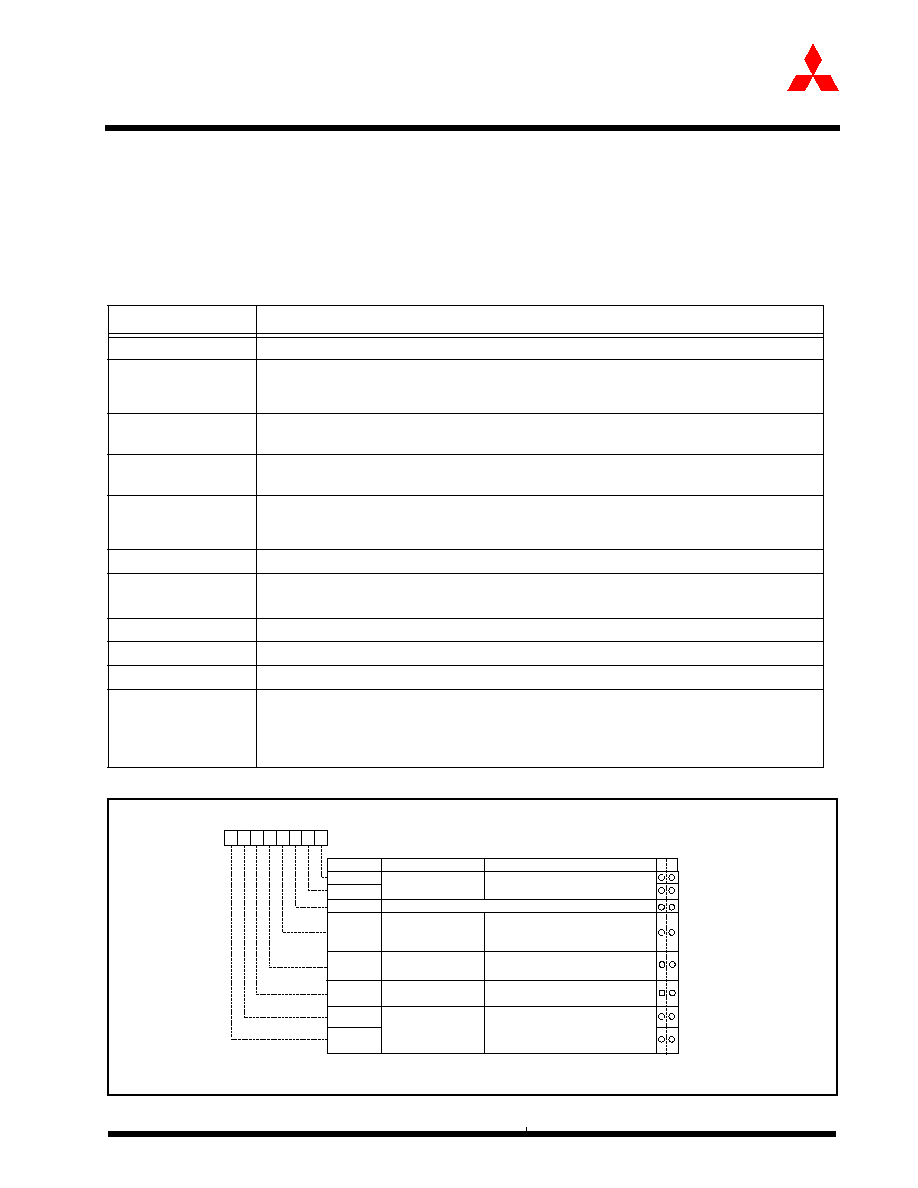
1-78
Mitsubishi microcomputers
M30240 Group
SINGLE-CHIP 16-BIT CMOS MICROCOMPUTER
Preliminary Specifications REV. E
Specifications in this manual are tentative and subject to change
Timer A
2.21.4 Pulse-width modulation (PWM) mode
In this mode, the timer outputs pulses of a given width in succession (See Table 1.21 ). In this mode,
the counter functions as either a 16-bit pulse-width modulator or an 8-bit pulse-width modulator. Figure
1.67 shows the timer Ai mode register in pulse-width modulation mode.Figure 1.68 shows the example
of how a 16-bit pulse-width modulator operates. Figure 1.69 shows the example of how an 8-bit pulse
width modulator operates.
Figure 1.67: Timer Ai mode register in pulse-width modulation mode
Table 1.21:
Timer specifications in pulse-width modulation mode
Item
Specification
Count source
f1, f8, f32
Count operation
�The timer counts down (operating as an 8-bit or a 16-bit pulse-width modulator)
�The timer reloads a new count at a rising edge of PWM pulse and continues counting
� The timer is not affected by a trigger that occurs when counting
16-bit PWM
�High level width n / f
i
n: Set value
�Cycle time (216-1) / f
i
fixed
8-bit PWM
�High level width n (m+1) /f
i
n: values set to timer Ai register's high-order address
�Cycle time (28-1) (m+1) /f
i
m: values set to timer Ai register's low-order address
Count start condition
�External trigger is input
�The timer overflows
�The count start flag is set (= 1)
Count stop condition
�The count start flag is reset (= 0)
Interrupt request
generation timing
PWM pulse goes "L"
TAiIN pin function
Programmable I/O port or trigger input
TAiOUT pin function
Pulse output
Read from timer
When timer Ai register is read, it indicates an indeterminate value
Write to timer
�When counting is stopped and a value is written to timer Ai register, it is written to both
reload register and the counter
�When counting in progress and a value is written to timer A register, it is written to only
reload register to be transferred to the counter at next reload timer.
Note 1: Valid only when the TAi
IN
pin is selected by the event/trigger select bit.
(addresses 0382
16
and 0383
16
). If timer overflow is selected, this bit can be "1", or "0".
Note 2: Set the corresponding port direction register to "0".
Timer Ai mode register
Symbol
Address
When reset
TAiMR(i=0 to 4)
0396
16
to 039A
16
00
16
Bit name
Function
Bit symbol
b7
b6
b5
b4
b3
b2
b1
b0
Operation mode
select bit
1 1 : PWM mode
b1 b0
TMOD1
TMOD0
MR0
External trigger select bit
(Note 1)
0 : Falling edge of TAi
IN
pin's input signal
(Note 2)
1 : Rising edge of TAi
IN
pin's input signal
(Note 2)
MR2
MR1
MR3
Must always be "1" in PWM mode)
0 0 : f
1
0 1 : f
8
1 0 : f
32
1 1 : Reserved
b7 b6
TCK1
TCK0
Count source select bit
1 1
1
W
R
Trigger select bit
0 : Functions as a 16-bit pulse width modulator
1 : Functions as an 8-bit pulse width modulator
16/8 PWM mode select bit
0 : Count strat flig is valid
1 : Selected by event /trigger select register
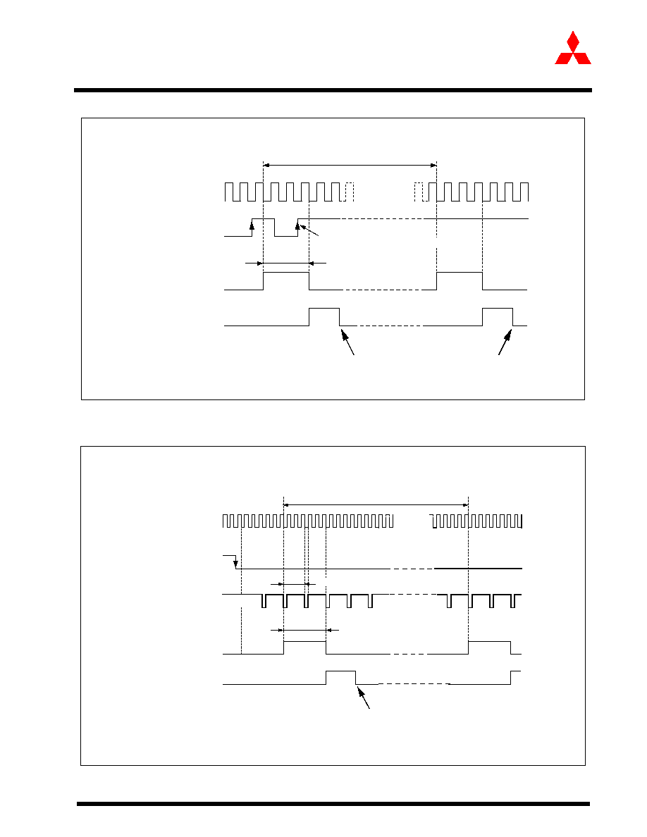
1-79
Mitsubishi microcomputers
M30240 Group
SINGLE-CHIP 16-BIT CMOS MICROCOMPUTER
Preliminary Specifications REV. E
Specifications in this manual are tentative and subject to change
Timer A
Figure 1.68: Example of how a 16-bit pulse-width modulator operates
Figure 1.69: Example of how an 8-bit pulse-width modulator operates
1 / f
i
X
(2 � 1)
16
Count source
TA
iIN
pin
input signal
PWM pulse output
from TA
iOUT
pin
Condition : Reload register = 0003
16
, when external trigger
(rising edge of TA
iIN
pin input signal) is selected
Trigger is not generated by this signal
"H"
"H"
"L"
"L"
Timer Ai interrupt
request bit
"1"
"0"
Cleared to "0" when interrupt request is accepted, or cleared by software
f
i
: Frequency of count source
(f
1
, f
8
, f
32
)
Note: n = 0000
16
to FFFE
16
.
1 / f
i
X
n
Count source (Note1)
TA
iIN
pin input signal
Underflow signal of
8-bit prescaler (Note2)
PWM pulse output
from TA
iOUT
pin
"H"
"H"
"H"
"L"
"L"
"L"
"1"
"0"
Timer Ai interrupt
request bit
Cleared to "0" when interrupt request is accepted, or cleared by software
f
i
: Frequency of count source
(f
1
, f
8
, f
32
)
Note 1: The 8-bit prescaler counts the count source.
Note 2: The 8-bit pulse width modulator counts the 8-bit prescaler's underflow signal.
Note 3: m = 00
16
to FE
16
; n = 00
16
to FE
16
.
Condition : Reload register high-order 8 bits = 02
16
Reload register low-order 8 bits = 02
16
External trigger (falling edge of TA
iIN
pin input signal) is selected
1 / f
i
X (m
+ 1) X (2 � 1)
8
1 / f
i
X (m + 1) X n
1 / f
i
X (m + 1)
1-80
Mitsubishi microcomputers
M30240 Group
SINGLE-CHIP 16-BIT CMOS MICROCOMPUTER
Preliminary Specifications REV. E
Specifications in this manual are tentative and subject to change
Timer B
2.22 Timer B
Figure 1.70 shows the block diagram of timer B. Figure 1.71 and Figure 1.72 show the timer B-related
registers. Use the timer Bi mode register (i = 0 to 2) bits 0 and 1 to choose the desired mode. Timer B
works in Timer mode only (i.e., the timer counts an in internal count source).
Figure 1.70: Block diagram of Timer B
Figure 1.71: Timer B-related registers
Clock source selection
(address 0380
16
)
Reload register (16)
Low-order 8 bits
High-order 8 bits
Data bus low-order bits
Data bus high-order bits
f
1
f
8
f
32
Count start flag
Counter reset circuit
Counter (16)
Address
0391
16
0390
16
0393
16
0392
16
0395
16
0394
16
TBi
Timer B0
Timer B1
Timer B2
TBj
Timer B2
Timer B0
Timer B1
TBj overflow
(j=i - 1. Note, however,
j = 2 when i = 0)
Note 1: Timer B0.
Note 2: Timer B1, Timer B2.
Timer Bi mode register
Symbol
Address
When reset
TBiMR(i=0 to 2) 039B
16
to 039D
16
00XX0000
2
Bit name
Function
Bit symbol
W
R
b7
b6
b5
b4
b3
b2
b1
b0
Operation mode select bit
0 0 : Timer mode
b1 b0
TMOD1
TMOD0
MR0
Invalid in timer mode
Can be "0" or "1"
MR2
MR1
MR3
0 0 : f
1
0 1 : f
8
1 0 : f
32
1 1 : Reserved
TCK1
TCK0
Count source select bit
0
Invalid in timer mode.
This bit can neither be set nor reset. When read in timer mode,
its content is indeterminate.
0
0 (Fixed to "0" in timer mode ; i = 0)
Nothing is assiigned (i = 1, 2).
This bit can neither be set nor reset. When read, its content is indeterminate.
(Note 1)
(Note 2)
b7 b6
1-81
Mitsubishi microcomputers
M30240 Group
SINGLE-CHIP 16-BIT CMOS MICROCOMPUTER
Preliminary Specifications REV. E
Specifications in this manual are tentative and subject to change
Timer B
Figure 1.72: Timer B-related registers
2.22.1 Timer mode
In this mode, the timer counts an internally generated count source. (See Table 1.22 ) Figure 1.73
shows the Timer Bi mode register in timer mode.
Note: Timer B2 does not generate an interrupt; it is used only as a prescaler.
Table 1.22:
Timer specifications in timer mode
Item
Specification
Count source
f1, f8, f32
Count operation
�Counts down
�When the timer underflows, it reloads the reload register contents before continuing
counting
Divide ratio
1/(n+1) n: Set value
Count start condition
Count start flag is set (= 1)
Count stop condition
Count start flag is reset (= 0)
Interrupt request
generation timing
The timer underflows (see Note)
Symbol
Address
When reset
TABSR
0380
16
00
16
Count start flag
Bit name
Bit symbol
W
R
b7
b6
b5
b4
b3
b2
b1
b0
Timer B2 count start flag
Timer B1 count start flag
Timer B0 count start flag
Timer A4 count start flag
Timer A3 count start flag
Timer A2 count start flag
Timer A1 count start flag
Timer A0 count start flag
0 : Stops counting
1 : Starts counting
TB2S
TB1S
TB0S
TA4S
TA3S
TA2S
TA1S
TA0S
Function
Symbol
Address
When reset
TB0
0391
16
, 0390
16
Indeterminate
TB1
0393
16
, 0392
16
Indeterminate
TB2
0395
16
, 0394
16
Indeterminate
TB3
0351
16
, 0350
16
Indeterminate
TB4
0353
16
, 0352
16
Indeterminate
TB5
0355
16
, 0354
16
Indeterminate
b7
b0 b7
b0
(b15)
(b8)
Timer Bi register (Note)
W
R
� Timer mode
0000
16
to FFFF
16
Counts the timer's period
Function
Values that can be set
Note: Read and write data in 16-bit units.
1-82
Mitsubishi microcomputers
M30240 Group
SINGLE-CHIP 16-BIT CMOS MICROCOMPUTER
Preliminary Specifications REV. E
Specifications in this manual are tentative and subject to change
Timer B
Figure 1.73: Timer Bi mode register in timer mode
Note 1: Timer B0.
Note 2: Timer B1, Timer B2.
Timer Bi mode register
Symbol
Address
When reset
TBiMR(i=0 to 2)
039B
16
to 039D
16
00XX0000
2
Bit name
Function
Bit symbol
W
R
b7
b6
b5
b4
b3
b2
b1
b0
Operation mode select bit
0 0 : Timer mode
b1 b0
TMOD1
TMOD0
MR0
Invalid in timer mode
Can be "0" or "1"
MR2
MR1
MR3
0 0 : f
1
0 1 : f
8
1 0 : f
32
1 1 : Reserved
TCK1
TCK0
Count source select bit
0
Invalid in timer mode.
In an attempt to write to this bit, write "0". The value, if read in
timer mode, turns out to be indeterminate.
0
0 (Fixed to "0" in timer mode ; i = 0)
Nothing is assiigned (i = 1, 2).
In an attempt to write to this bit, write "0". The value, if read, turns out
to be indeterminate.
(Note 1)
(Note 2)
b7 b6
1-83
Mitsubishi microcomputers
M30240 Group
SINGLE-CHIP 16-BIT CMOS MICROCOMPUTER
Preliminary Specifications REV. E
Specifications in this manual are tentative and subject to change
UART0 through UART2
2.23 UART0 through UART2
Serial I/O is configured as three channels: UART0, UART1, and UART2. UART0, UART1, and UART2
each have an exclusive timer to generate a transfer clock, so they operate independently of each other.
Figure 1.74 shows the block diagram of UART0, UART1, and UART2.
Figure 1.74: Block diagram of UARTi (i=0 to 2)
n0 : Values set to UART0 bit rate generator (BRG0)
n1 : Values set to UART1 bit rate generator (BRG1)
n2 : Values set to UART2 bit rate generator (BRG2)
RxD
2
Reception
control circuit
Transmission
control circuit
1 / (n
2
+1)
1/16
1/16
1/2
Bit rate generator
(address 0379
16
)
Clock synchronous type
(when internal clock is selected)
UART reception
Clock synchronous type
UART transmission
Clock synchronous type
Clock synchronous type
(when internal clock is selected)
Clock synchronous type
(when external clock is
selected)
Receive
clock
Transmit
clock
CLK
2
CTS
2
/ RTS
2
f
1
f
8
f
32
Vcc
RTS
2
CTS
2
TxD
2
(UART2)
RxD polarity
reversing circuit
TxD
polarity
reversing
circuit
RxD
0
1 / (n
0
+1)
1/2
Bit rate generator
(address 03A1
16
)
Clock synchronous type
(when internal clock is selected)
UART reception
Clock synchronous type
UART transmission
Clock synchronous type
Clock synchronous type
(when internal clock is selected)
Clock synchronous type
(when external clock is
selected)
Receive
clock
Transmit
clock
CLK
0
Clock source selection
CTS
0
/ RTS
0
f
1
f
8
f
32
Reception
control circuit
Transmission
control circuit
Internal
External
RTS
0
CTS
0
TxD
0
Transmit/
receive
unit
RxD
1
1 / (n
1
+1)
1/16
1/16
1/2
Bit rate generator
(address 03A9
16
)
Clock synchronous type
(when internal clock is selected)
UART reception
Clock synchronous type
UART transmission
Clock synchronous type
Clock synchronous type
(when internal clock is selected)
Clock synchronous type
(when external clock is
selected)
Receive
clock
Transmit
clock
CLK
1
Clock source selection
f
1
f
8
f
32
Reception
control circuit
Transmission
control circuit
Internal
External
RTS
1
CTS
1
TxD
1
(UART1)
(UART0)
CLK
polarity
reversing
circuit
CLK
polarity
reversing
circuit
CTS/RTS disabled
Clock output pin
select switch
CTS
1
/ RTS
1
CLKS
1
CTS/RTS disabled
CTS/RTS selected
CTS/RTS disabled
V
CC
CTS/RTS disabled
CTS/RTS disabled
CTS/RTS disabled
CTS/RTS
selected
CLK
polarity
reversing
circuit
Internal
External
Clock source selection
Transmit/
receive
unit
Transmit/
receive
unit
1/16
1/16
V
CC

1-84
Mitsubishi microcomputers
M30240 Group
SINGLE-CHIP 16-BIT CMOS MICROCOMPUTER
Preliminary Specifications REV. E
Specifications in this manual are tentative and subject to change
UART0 through UART2
Figure 1.75 and Figure 1.76 show the block diagram of the transmit/receive unit.
Figure 1.75: Block diagram of UARTi (i=0,1) transmit/receive circuit
Figure 1.76: Block diagram of UART2 transmit/receive circuit
SP
SP
PAR
2SP
1SP
UART
UART (7 bits)
UART (8 bits)
UART (7 bits)
UART (9 bits)
Clock
synchronous
type
Clock synchronous
type
TxDi
UARTi transmit register
PAR
enabled
PAR
disabled
D
8
D
7
D
6
D
5
D
4
D
3
D
2
D
1
D
0
SP: Stop bit
PAR: Parity bit
UARTi transmit
buffer register
MSB/LSB conversion circuit
UART (8 bits)
UART (9 bits)
Clock synchronous
type
UARTi receive
buffer register
UARTi receive register
2SP
1SP
PAR
enabled
PAR
disabled
UART
UART (7 bits)
UART (9 bits)
Clock
synchronous
type
Clock
synchronous type
UART (7 bits)
UART (8 bits)
RxDi
Clock
synchronous type
UART (8 bits)
UART (9 bits)
Address 03A6
16
Address 03A7
16
Address 03AE
16
Address 03AF
16
Address 03A2
16
Address 03A3
16
Address 03AA
16
Address 03AB
16
Data bus low-order bits
MSB/LSB conversion circuit
D
7
D
6
D
5
D
4
D
3
D
2
D
1
D
0
D
8
0
0
0
0
0
0
0
SP
SP
PAR
"0"
Data bus high-order bits
SP
SP
PAR
2SP
1SP
UART
UART
(7 bits)
UART
(8 bits)
UART(7 bits)
UART
(9 bits)
Clock
synchronous
type
Clock
synchronous type
Data bus low-order bits
TxD2
UART2 transmit register
PAR
disabled
PAR
enabled
D
8
D
7
D
6
D
5
D
4
D
3
D
2
D
1
D
0
UART2 transmit
buffer register
UART
(8 bits)
UART
(9 bits)
Clock
synchronous type
UART2 receive
buffer register
UART2 receive register
2SP
1SP
UART
(7 bits)
UART
(8 bits)
UART(7 bits)
UART
(9 bits)
Clock
synchronous type
Clock
synchronous type
RxD2
UART
(8 bits)
UART
(9 bits)
Address 037E16
Address 037F16
Address 037A16
Address 037B16
Data bus high-order bits
D
7
D
6
D
5
D
4
D
3
D
2
D
1
D
0
D
8
0
0
0
0
0
0
0
SP
SP
PAR
"0"
Reverse
No reverse
Error signal
output circuit
RxD data
reverse circuit
Error signal output
enable
Error signal output
disable
Reverse
No reverse
Logic reverse circuit + MSB/LSB conversion circuit
Logic reverse circuit + MSB/LSB conversion circuit
PAR
enabled
PAR
disabled
UART
Clock
synchronous
type
TxD data
reverse circuit
SP: Stop bit
PAR: Parity bit
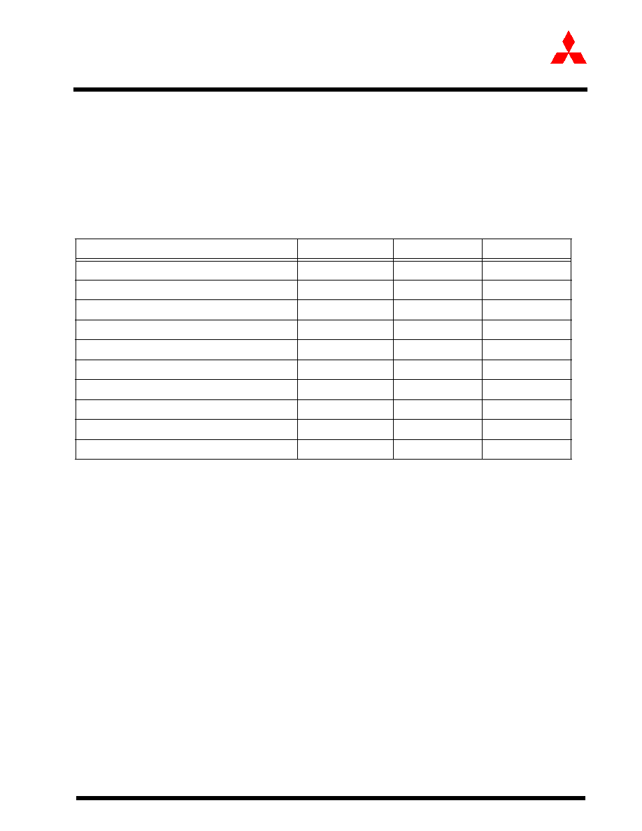
1-85
Mitsubishi microcomputers
M30240 Group
SINGLE-CHIP 16-BIT CMOS MICROCOMPUTER
Preliminary Specifications REV. E
Specifications in this manual are tentative and subject to change
UART0 through UART2
UARTi (i = 0 to 2) has two operation modes: a clock synchronous serial I/O mode and a clock
asynchronous serial I/O mode (UART mode). The contents of the serial I/O mode select bits (bits 0 to 2
at addresses 03A0
16
, 03A8
16
and 0378
16
) determine whether UARTi is used as a clock synchronous
serial I/O or as a UART. Although a few functions are different, UART0 and UART1 have almost the
same functions.
UART0 through UART2 are almost equal in their functions with minor exceptions.Table 1.23 shows the
comparison of functions of UART0 through UART2, and Figure 1.77, Figure 1.78, Figure 1.79, Figure
1.80, and Figure 1.81 show the registers related to UARTi.
Note 1: Only during clock synchronous serial I/O mode.
Note 2: Only during clock synchronous serial I/O mode and 8-bit UART mode.
Note 3: Only during UART mode.
Note 4: Used for SIM interface.
Table 1.23:
Comparison of functions of UART0 through UART2
Function
UART0
UART1
UART2
CLK polarity selection
Possible (Note 1)
Possible (Note 1)
Possible (Note 1)
LSB first / MSB first selection
Possible (Note 1)
Possible (Note 1)
Possible (Note 2)
Continuous receive mode selection
Possible (Note 1)
Possible (Note 1)
Possible (Note 1)
Transfer clock output from multiple pins selection
Impossible
Possible (Note 1)
Impossible
Serial data logic switch
Impossible
Impossible
Possible (Note 4)
Sleep mode selection
Possible (Note 3)
Possible (Note 3)
Impossible
TxD, RxD I/O polarity switch
Impossible
Impossible
Possible
TxD, RxD port output format
CMOS output
CMOS output
CMOS output
Parity error signal output
Impossible
Impossible
Possible (Note 4)
Bus collision detection
Impossible
Impossible
Possible
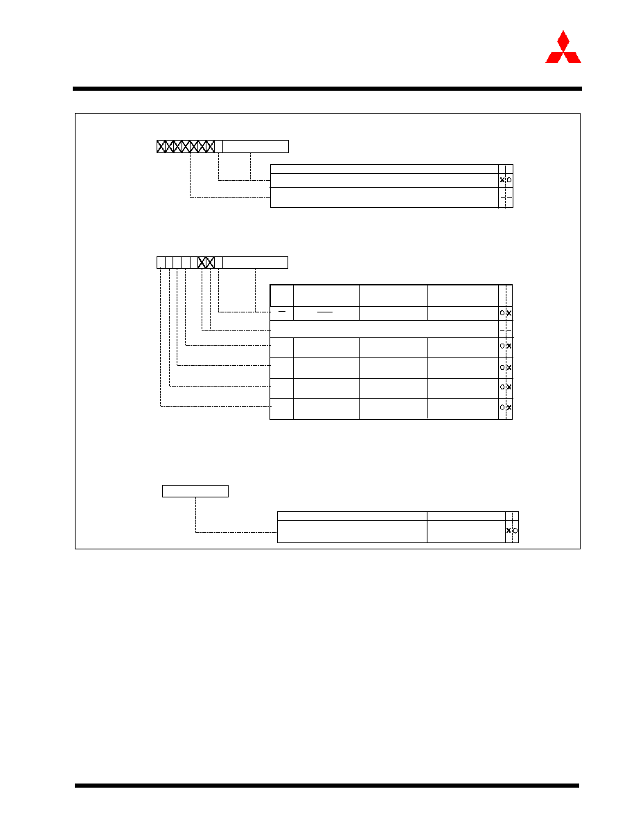
1-86
Mitsubishi microcomputers
M30240 Group
SINGLE-CHIP 16-BIT CMOS MICROCOMPUTER
Preliminary Specifications REV. E
Specifications in this manual are tentative and subject to change
UART0 through UART2
Figure 1.77: Serial I/O-related registers (1)
b7
UARTi bit rate generator
b0
Symbol
Address
When reset
U0BRG
03A1
16
Indeterminate
U1BRG
03A9
16
Indeterminate
U2BRG
0379
16
Indeterminate
Function
Assuming that set value = n, BRGi divides the count source by
n + 1
00
16
to FF
16
Values that can be set
W
R
b7
b0
(b15)
(b8)
b7
b0
UARTi transmit buffer register
Function
Transmit data
Nothing is assigned.
These bits can neither be set nor reset. When read, their contents are indeterminate.
Symbol
Address
When reset
U0TB
03A3
16
, 03A2
16
Indeterminate
U1TB
03AB
16
, 03AA
16
Indeterminate
U2TB
037B
16
, 037A
16
Indeterminate
W
R
(b15)
Symbol
Address
When reset
U0RB
03A7
16
, 03A6
16
Indeterminate
U1RB
03AF
16
, 03AE
16
Indeterminate
U2RB
037F
16
, 037E
16
Indeterminate
b7
b0
(b8)
b7
b0
UARTi receive buffer register
Function
(During UART mode)
Function
(During clock synchronous
serial I/O mode)
Bit name
Bit
symbol
0 : No framing error
1 : Framing error found
0 : No parity error
1 : Parity error found
0 : No error
1 : Error found
Note 1: Bits 15 through 12 are set to "0" when the serial I/O mode select bit (bits 2 to 0 at addresses 03A0
16
,
03A8
16
and 0378
16
) are set to "000
2
" or the receive enable bit is set to "0".
(Bit 15 is set to "0" when bits 14 to 12 all are set to "0".) Bits 14 and 13 are also set to "0" when the
lower byte of the UARTi receive buffer register (addresses 03A6
16
, 03AE
16
and 037E
16
) is read out.
Invalid
Invalid
Invalid
OER
FER
PER
SUM
Overrun error flag (Note 1)
Framing error flag (Note 1)
Parity error flag (Note 1)
Error sum flag (Note 1)
0 : No overrun error
1 : Overrun error found
0 : No overrun error
1 : Overrun error found
Nothing is assigned.
These bits can neither be set nor reset. When read, the value of these bits is "0".
Receive data
W
R
Receive data
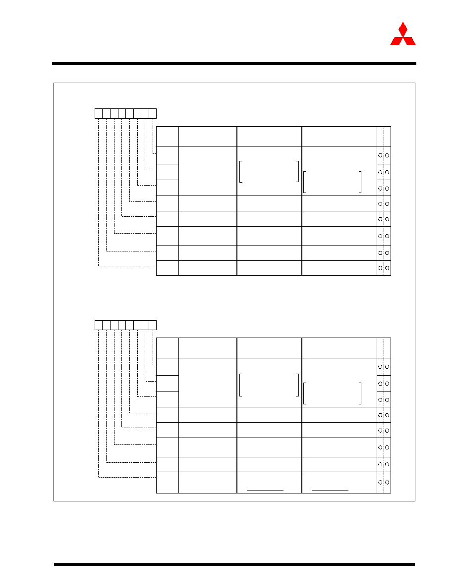
1-87
Mitsubishi microcomputers
M30240 Group
SINGLE-CHIP 16-BIT CMOS MICROCOMPUTER
Preliminary Specifications REV. E
Specifications in this manual are tentative and subject to change
UART0 through UART2
Figure 1.78: Serial I/O-related registers (2)
UARTi transmit/receive mode register
Symbol
Address
When reset
UiMR(i=0,1)
03A0
16
, 03A8
16
00
16
b7
b6
b5
b4
b3
b2
b1
b0
Bit name
Bit
symbol
W
R
Must be fixed to 001
0 0 0 : Serial I/O invalid
0 1 0 : Inhibited
0 1 1 : Inhibited
1 1 1 : Inhibited
b2 b1 b0
CKDIR
SMD1
SMD0
Serial I/O mode select bit
SMD2
Internal/external clock
select bit
STPS
PRY
PRYE
SLEP
Parity enable bit
0 : Internal clock
1 : External clock
Stop bit length select bit
Odd/even parity select bit
Sleep select bit
0 : One stop bit
1 : Two stop bits
0 : Parity disabled
1 : Parity enabled
0 : Sleep mode deselected
1 : Sleep mode selected
1 0 0 : Transfer data 7 bits long
1 0 1 : Transfer data 8 bits long
1 1 0 : Transfer data 9 bits long
0 0 0 : Serial I/O invalid
0 1 0 : Inhibited
0 1 1 : Inhibited
1 1 1 : Inhibited
b2 b1 b0
0 : Internal clock
1 : External clock
Invalid
Valid when bit 6 = "1"
0 : Odd parity
1 : Even parity
Invalid
Invalid
Must always be "0"
Function
(During UART mode)
Function
(During clock synchronous
serial I/O mode)
UART2 transmit/receive mode register
Symbol
Address
When reset
U2MR
0378
16
00
16
b7
b6
b5
b4
b3
b2
b1
b0
Bit name
Bit
symbol
W
R
Must be fixed to 001
0 0 0 : Serial I/O invalid
0 1 1 : Inhibited
1 1 1 : Inhibited
b2 b1 b0
CKDIR
SMD1
SMD0
Serial I/O mode select bit
SMD2
Internal/external clock
select bit
STPS
PRY
PRYE
IOPOL
Parity enable bit
0 : Internal clock
1 : External clock
Stop bit length select bit
Odd/even parity select bit
TxD, RxD I/O polarity
reverse bit
0 : One stop bit
1 : Two stop bits
0 : Parity disabled
1 : Parity enabled
0 : No reverse
1 : Reverse
Usually set to "0"
1 0 0 : Transfer data 7 bits long
1 0 1 : Transfer data 8 bits long
1 1 0 : Transfer data 9 bits long
0 0 0 : Serial I/O invalid
0 1 1 : Inhibited
1 1 1 : Inhibited
b2 b1 b0
0 : Internal clock
1 : External clock
Invalid
Valid when bit 6 = "1"
0 : Odd parity
1 : Even parity
Invalid
Invalid
0 : No reverse
1 : Reverse
Usually set to "0"
Function
(During UART mode)
Function
(During clock synchronous
serial I/O mode)
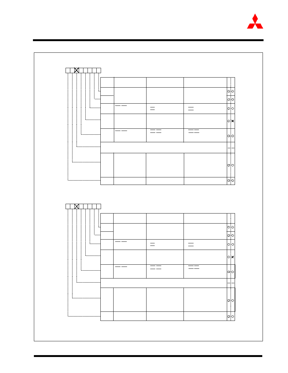
1-88
Mitsubishi microcomputers
M30240 Group
SINGLE-CHIP 16-BIT CMOS MICROCOMPUTER
Preliminary Specifications REV. E
Specifications in this manual are tentative and subject to change
UART0 through UART2
Figure 1.79: Serial I/O-related registers (3)
UARTi transmit/receive control register 0
Symbol
Address
When reset
UiC0(i=0,1)
03A4
16
, 03AC
16
08
16
b7
b6
b5
b4
b3
b2
b1
b0
Function
(During UART mode)
W
R
Function
(During clock synchronous
serial I/O mode)
TXEPT
CLK1
CLK0
CRS
CRD
CKPOL
BRG count source
select bit
Transmit register empty
flag
0 : Transmit data is output at
falling edge of transfer clock
and receive data is input at
rising edge
1 : Transmit data is output at
rising edge of transfer clock
and receive data is input at
falling edge
CLK polarity select bit
CTS/RTS function
select bit
CTS/RTS disable bit
0 0 : f
1
is selected
0 1 : f
8
is selected
1 0 : f
32
is selected
1 1 : Reserved
b1 b0
0 : LSB first
1 : MSB first
0 : Data present in transmit
register (during transmission)
1 : No data present in transmit
register (transmission
completed)
0 : CTS/RTS function enabled
1 : CTS/RTS function disabled
(P6
0
and P6
4
function as
programmable I/O port)
UFORM Transfer format select bit
0 0 : f
1
is selected
0 1 : f
8
is selected
1 0 : f
32
is selected
1 1 : Reserved
b1 b0
Valid when bit 4 = "0"
0 : CTS function is selected (Note 1)
1 : RTS function is selected (Note 2)
Valid when bit 4 = "0"
0 : CTS function is selected (Note 1)
1 : RTS function is selected (Note 2)
0 : Data present in transmit register
(during transmission)
1 : No data present in transmit
register (transmission completed)
Must always be "0"
Bit name
Bit
symbol
Must always be "0"
Note 1: Set the corresponding port direction register to "0".
Note 2: The settings of the corresponding port register and port direction register are invalid.
0 : CTS/RTS function enabled
1 : CTS/RTS function disabled
(P6
0
and P6
4
function as
programmable I/O port)
UART2 transmit/receive control register 0
Symbol
Address
When reset
U2C0
037C
16
08
16
b7
b6
b5
b4
b3
b2
b1
b0
Function
(During UART mode)
W
R
Function
(During clock synchronous
serial I/O mode)
TXEPT
CLK1
CLK0
CRS
CRD
CKPOL
BRG count source
select bit
Transmit register empty
flag
0 : Transmit data is output at
falling edge of transfer clock
and receive data is input at
rising edge
1 : Transmit data is output at
rising edge of transfer clock
and receive data is input at
falling edge
CLK polarity select bit
CTS/RTS function
select bit
CTS/RTS disable bit
0 0 : f
1
is selected
0 1 : f
8
is selected
1 0 : f
32
is selected
1 1 : Inhibited
b1 b0
0 : LSB first
1 : MSB first
0 : Data present in transmit
register (during transmission)
1 : No data present in transmit
register (transmission
completed)
0 : CTS/RTS function enabled
1 : CTS/RTS function disabled
(P7
3
functions
programmable I/O port)
0 : TXDi pin is CMOS output
1 : TXDi pin is N-channel
open-drain output
UFORM Transfer format select bit
(Note 3)
0 0 : f
1
is selected
0 1 : f
8
is selected
1 0 : f
32
is selected
1 1 : Inhibited
b1 b0
Valid when bit 4 = "0"
0 : CTS function is selected (Note 1)
1 : RTS function is selected (Note 2)
Valid when bit 4 = "0"
0 : CTS function is selected (Note 1)
1 : RTS function is selected (Note 2)
0 : Data present in transmit register
(during transmission)
1 : No data present in transmit
register (transmission completed)
0: TXDi pin is CMOS output
1: TXDi pin is N-channel
open-drain output
Must always be "0"
Bit name
Bit
symbol
Note 1: Set the corresponding port direction register to "0".
Note 2: The settings of the corresponding port register and port direction register are invalid.
Note 3: Only clock synchronous serial I/O mode and 8-bit UART mode are valid.
0 : CTS/RTS function enabled
1 : CTS/RTS function disabled
(P7
3
functions programmable
I/O port)
Nothing is assigned.
This bit can neither be set nor reset. When read, the value of this bit is "0".
0 : LSB first
1 : MSB first
Nothing is assigned.
This bit can neither be set nor reset. When read, the value of this bit is "0".

1-89
Mitsubishi microcomputers
M30240 Group
SINGLE-CHIP 16-BIT CMOS MICROCOMPUTER
Preliminary Specifications REV. E
Specifications in this manual are tentative and subject to change
UART0 through UART2
Figure 1.80: Serial I/O-related registers (4)
UARTi transmit/receive control register 1
Symbol
Address
When reset
UiC1(i=0,1)
03A5
16
,
03AD
16
02
16
b7
b6
b5
b4
b3
b2
b1
b0
Bit name
Bit
symbol
W
R
Function
(During UART mode)
Function
(During clock synchronous
serial I/O mode)
TE
TI
RE
RI
Transmit enable bit
Receive enable bit
Receive complete flag
Transmit buffer
empty flag
0 : Transmission disabled
1 : Transmission enabled
0 : Data present in
transmit buffer register
1 : No data present in
transmit buffer register
0 : Reception disabled
1 : Reception enabled
0 : Transmission disabled
1 : Transmission enabled
0 : Data present in
transmit buffer register
1 : No data present in
transmit buffer register
0 : Reception disabled
1 : Reception enabled
0 : No data present in
receive buffer register
1 : Data present in
receive buffer register
0 : No data present in
receive buffer register
1 : Data present in
receive buffer register
Nothing is assigned.
These bits can neither be set nor reset. When read, the value of these bits is "0".
UART2 transmit/receive control register 1
Symbol
Address
When reset
U2C1
037D
16
02
16
b7
b6
b5
b4
b3
b2
b1
b0
Bit name
Bit
symbol
W
R
Function
(During UART mode)
Function
(During clock synchronous
serial I/O mode)
TE
TI
RE
RI
Transmit enable bit
Receive enable bit
Receive complete flag
Transmit buffer
empty flag
0 : Transmission disabled
1 : Transmission enabled
0 : Data present in
transmit buffer register
1 : No data present in
transmit buffer register
0 : Reception disabled
1 : Reception enabled
0 : Transmission disabled
1 : Transmission enabled
0 : Data present in
transmit buffer register
1 : No data present in
transmit buffer register
0 : Reception disabled
1 : Reception enabled
0 : No data present in
receive buffer register
1 : Data present in
receive buffer register
0 : No data present in
receive buffer register
1 : Data present in
receive buffer register
U2IRS
UART2 transmit interrupt
cause select bit
0 : Transmit buffer empty
(TI = 1)
1 : Transmit is completed
(TXEPT = 1)
0 : Transmit buffer empty
(TI = 1)
1 : Transmit is completed
(TXEPT = 1)
U2RRM UART2 continuous
receive mode enable bit
0 : Continuous receive
mode disabled
1 : Continuous receive
mode enabled
Invalid
Data logic select bit
0 : No reverse
1 : Reverse
0 : No reverse
1 : Reverse
U2LCH
U2ERE Error signal output
enable bit
Must be fixed to "0"
0 : Output disabled
1 : Output enabled
1-90
Mitsubishi microcomputers
M30240 Group
SINGLE-CHIP 16-BIT CMOS MICROCOMPUTER
Preliminary Specifications REV. E
Specifications in this manual are tentative and subject to change
UART0 through UART2
Figure 1.81: Serial I/O-related registers (5)
Note: When using multiple pins to output the transfer clock, the following requirements must be met:
� UART1 internal/external clock select bit (bit 3 at address 03A8
16
) = "0".
UART transmit/receive control register 2
Symbol
Address
When reset
UCON
03B0
16
X0000000
2
b7
b6
b5
b4
b3
b2
b1
b0
Bit name
Bit
symbol
W
R
Function
(During UART mode)
Function
(During clock synchronous
serial I/O mode)
CLKMD0
CLKMD1
UART0 transmit
interrupt cause select bit
UART0 continuous
receive mode enable bit
0 : Continuous receive
mode disabled
1 : Continuous receive
mode enable
UART1 continuous
receive mode enable bit
CLK/CLKS select bit 0
UART1 transmit
interrupt cause select bit
0 :
Transmit buffer empty (Tl = 1)
1 : Transmission completed
(TXEPT = 1)
0 :
Transmit buffer empty (Tl = 1)
1 : Transmission completed
(TXEPT = 1)
0 : Normal mode
(CLK output is CLK1 only)
1 : Transfer clock output
from multiple pins
function selected
0 : Continuous receive
mode disabled
1 : Continuous receive
mode enabled
Nothing is assigned.
This bit can neither be set nor reset. When read, its content is indeterminate.
0 : Transmit buffer empty (Tl = 1)
1 : Transmission completed
(TXEPT = 1)
0 : Transmit buffer empty (Tl = 1)
1 : Transmission completed
(TXEPT = 1)
Must always be "0"
U0IRS
U1IRS
U0RRM
U1RRM
Invalid
Invalid
Invalid
CLK/CLKS select
bit 1 (Note)
Valid when bit 5 = "1"
0 : Clock output to CLK1
1 : Clock output to CLKS1
Must always be "0"
Reserved
Must always be "0"

1-91
Mitsubishi microcomputers
M30240 Group
SINGLE-CHIP 16-BIT CMOS MICROCOMPUTER
Preliminary Specifications REV. E
Specifications in this manual are tentative and subject to change
UART0 through UART2
2.23.1 Clock synchronous serial I/O mode
The clock synchronous serial I/O mode uses a transfer clock to transmit and receive data. Table 1.24
and Table 1.25 list the specifications of the clock synchronous serial I/O mode. Figure 1.82 shows the
UARTi transmit/receive mode register.
Note 1: "n" denotes the value 00
16
to FF
16
that is set to the UART bit rate generator.
Note 2: Maximum 5 Mbps.
Note 3: If an overrun error occurs, the UARTi receive buffer will have the next data written in. Note also that the UARTi
receive interrupt request bit is not set to "1".
Table 1.24:
Specifications of clock synchronous serial I/O mode (1)
Item
Specification
Transfer data format
� Transfer data length: 8 bits
Transfer clock
� When internal clock is selected (bit 3 at addresses 03A0
16
, 03A8
16
, 0378
16
= "0"): fi=2(n+1)
(Note 1) fi = f1, f8, f32
� When external clock is selected (bit 3 at addresses 03A0
16
, 03A8
16
, 0378
16
= "1"): Input
from CLKi pin (Note 2)
Transmission/reception
control
� CTS function/RTS function/CTS, RTS function chosen to be invalid
Transmission start
condition
� To start transmission, the following requirements must be met:
_ Transmit enable bit (bit 0 at addresses 03A5
16
, 03AD
16
, 037D
16
) = "1"
_ Transmit buffer empty flag (bit 1 at addresses 03A5
16
, 03AD
16
, 037D
16
) = "0"
_ When CTS function selected, CTS input level = "L"
� Furthermore, if external clock is selected, the following requirements must also be met:
_ CLKi polarity select bit (bit 6 at addresses 03A4
16
, 03AC
16
, 037C
16
) = "0":
CLKi input level = "H"
_ CLKi polarity select bit (bit 6 at addresses 03A4
16
, 03AC
16
, 037C
16
) = "1":
CLKi input level = "L"
Reception start
condition
� To start reception, the following requirements must be met:
_ Receive enable bit (bit 2 at addresses 03A5
16
, 03AD
16
, 037D
16
) = "1"
_ Transmit enable bit (bit 0 at addresses 03A5
16
, 03AD
16
, 037D
16)
= "1"
_ Transmit buffer empty flag (bit 1 at addresses 03A5
16
, 03AD
16
, 037D
16
) = "0"
� Furthermore, if external clock is selected, the following requirements must
also be met:
_ CLKi polarity select bit (bit 6 at addresses 03A4
16
, 03AC
16
, 037C
16
) = "0":
CLKi input level = "H"
_ CLKi polarity select bit (bit 6 at addresses 03A4
16
, 03AC
16
, 037C
16
) = "1":
CLKi input level = "L"
� When transmitting
_ Transmit interrupt cause select bit (bits 0, 1 at address 03B0
16
, bit 4 at
address 037D
16
) = "0": Interrupts requested when data transfer from UARTi
_ Transmit interrupt cause select bit (bits 0, 1 at address 03B0
16
, bit 4 at
address 037D
16
) = "1": Interrupts requested when data transmission from
Error detection
� Overrun error (Note 3)
This error occurs when the next data is ready before contents of UARTi receive buffer is read.

1-92
Mitsubishi microcomputers
M30240 Group
SINGLE-CHIP 16-BIT CMOS MICROCOMPUTER
Preliminary Specifications REV. E
Specifications in this manual are tentative and subject to change
UART0 through UART2
Figure 1.82: UARTi transmit/receive mode register in clock synchronous serial I/O mode
Table 1.25:
Specifications of clock synchronous serial I/O mode (2)
Item
Specification
Select function
� CLK polarity selection
Whether transmit data is output/input at the rising edge or falling edge of the transfer clock can be
selected
� LSB first/MSB first selection
Whether transmission/reception begins with bit 0 or bit 7 can be selected
� Continuous receive mode selection
Reception is enabled simultaneously by a read from the receive buffer register
� Transfer clock output from multiple pins selection (UART1)
UART1 transfer clock can be chosen by software to be output from one of the two pins set
� Switching serial data logic (UART2)
Whether to reverse data in writing to the transmission buffer register or reading the reception buffer
register can be selected.
� Switching serial data logic (UART2)
This function is reversing TxD port output and RxD port input. All I/O data level is reversed.
Symbol
Address
When reset
UiMR(i=0,1)
03A0
16
, 03A8
16
00
16
CKDIR
UARTi transmit/receive mode registers
Internal/external clock
select bit
STPS
PRY
PRYE
SLEP
0 : Internal clock
1 : External clock
Bit name
Function
Bit symbol
W
R
b7
b6
b5
b4
b3
b2
b1
b0
0 (Must always be "0" in clock synchronous serial I/O mode)
0 1
0
SMD0
SMD1
SMD2
Serial I/O mode select bit
0 0 1 : Clock synchronous serial
I/O mode
b2 b1 b0
0
Invalid in clock synchronous serial I/O mode
Symbol
Address
When reset
U2MR
0378
16
00
16
CKDIR
UART2 transmit/receive mode register
Internal/external clock
select bit
STPS
PRY
PRYE
IOPOL
0 : Internal clock
1 : External clock
Bit name
Function
Bit symbol
W
R
b7
b6
b5
b4
b3
b2
b1
b0
0 1
0
SMD0
SMD1
SMD2
Serial I/O mode select bit
0 0 1 : Clock synchronous serial
I/O mode
b2 b1 b0
0
Invalid in clock synchronous serial I/O mode
TxD, RxD I/O polarity
reverse bit (Note)
0 : No reverse
1 : Reverse
Note: Usually set to "0".
1-93
Mitsubishi microcomputers
M30240 Group
SINGLE-CHIP 16-BIT CMOS MICROCOMPUTER
Preliminary Specifications REV. E
Specifications in this manual are tentative and subject to change
UART0 through UART2
Table 1.26 lists the functions of the input/output pins during clock synchronous serial I/O mode. This
table shows the pin functions when the transfer clock output from multiple pins function is not selected.
Note that for a period from when the UARTi operation mode is selected to when transfer starts, the
TxD pin outputs a "H". The typical clock synchronous timing diagrams are shown in Figure 1.83.
Table 1.26:
Input/output pin functions in clock synchronous serial I/O mode
Pin name
Function
Method of selection
TxDi
(P63, P67, P70)
Serial data
output
(Outputs dummy data when performing reception only)
RxDi
(P62, P66, P71)
Serial data
input
Port P62, P66, and P71 direction register (bits 2 and 6 at address 03EE
16
bit 1
at address 03EF
16
)= "0"
(Can be used as an input port when performing transmission only.)
CLKi
(P61, P65, P72)
Transfer clock
output
Internal/external clock select bit (bit 3 at address 03A0
16
, 03A8
16
, 0378
16
) = "0"
Transfer clock
input
Internal/external clock select bit (bit 3 at address 03A0
16
, 03A8
16
, 0378
16
) = "1"
Port P61, P65, and P72 direction register (bits 1 and 5 at address 03EE
16
, bit 2
at address 03EF
16
) = "0"
CTSi/RTSi
(P60,P64,P73)
CTS input
CTS/RTS disable bit (bit 4 at address 03A4
16
, 03AC
16
, 037C
16
) = "0"
CTS/RTS function select bit (bit 2 at address 03A4
16
, 03AC
16
, 037C
16
) = "0"
Port P60, P64 and P73 direction register (bits 0 and 4 at address 03EE
16
, bit 3
at address 03EF
16
) = "0"
RTS output
CTS/RTS disable bit (bit 4 at address 03A4
16
, 03AC
16
, 037C
16
) = "0"
CTS/RTS function select bit (bit 2 at address 03A4
16
, 03AC
16
, 037C
16
) = "1"
Programmable
I/O port
CTS/RTS disable bit (bit 4 at address 03A4
16
, 03AC
16
, 037C
16
) = "1"
1-94
Mitsubishi microcomputers
M30240 Group
SINGLE-CHIP 16-BIT CMOS MICROCOMPUTER
Preliminary Specifications REV. E
Specifications in this manual are tentative and subject to change
UART0 through UART2
Figure 1.83: Typical transmit/receive timings in clock synchronous serial I/O mode Polarity select
function
D
0
D
1
D
2
D
3
D
4
D
5
D
6
D
7
D
0
D
1
D
2
D
3
D
4
D
5
D
6
D
7
D
0
D
1
D
2
D
3
D
4
D
5
D
6
D
7
Tc
T
CLK
Stopped pulsing because transfer enable bit = "0"
Data is set in UARTi transmit buffer register
Tc = TCLK = 2(n + 1) / fi
fi: frequency of BRGi count source (f
1
, f
8
, f
32
)
n: value set to BRGi
Transfer clock
Transmit enable
bit (TE)
Transmit buffer
empty flag (Tl)
CLKi
TxDi
Transmit
register empty
flag (TXEPT)
"H"
"L"
"0"
"1"
"0"
"1"
"0"
"1"
CTSi
The above timing applies to the following settings:
� Internal clock is selected.
� CTS function is selected.
� CLK polarity select bit = "0".
� Transmit interrupt cause select bit = "0".
Transmit interrupt
request bit (IR)
"0"
"1"
Stopped pulsing because CTS = "H"
1 / f
EXT
Dummy data is set in UARTi transmit buffer register
Transmit enable
bit (TE)
Transmit buffer
empty flag (Tl)
CLKi
RxDi
Receive complete
flag (Rl)
RTSi
"H"
"L"
"0"
"1"
"0"
"1"
"0"
"1"
Receive enable
bit (RE)
"0"
"1"
Receive data is taken in
Transferred from UARTi transmit buffer register to UARTi transmit register
Read out from UARTi receive buffer register
The above timing applies to the following settings:
� External clock is selected.
� RTS function is selected.
� CLK polarity select bit = "0".
f
EXT
: frequency of external clock
Transferred from UARTi receive register
to UARTi receive buffer register
Receive interrupt
request bit (IR)
"0"
"1"
D
0
D
1
D
2
D
3
D
4
D
5
D
6
D
7
D
0
D
1
D
2
D
3
D
4
D
5
Shown in ( ) are bit symbols.
Transferred from UARTi transmit buffer register to UARTi transmit register
Meet the following conditions are met when the CLK
input before data reception = "H"
� Transmit enable bit "1"
� Receive enable bit "1"
� Dummy data write to UARTi transmit buffer register
Shown in ( ) are bit symbols.
Cleared to "0" when interrupt request is accepted, or cleared by software
Cleared to "0" when interrupt request is accepted, or cleared by software
Example of receive timing (when external clock is selected)

1-95
Mitsubishi microcomputers
M30240 Group
SINGLE-CHIP 16-BIT CMOS MICROCOMPUTER
Preliminary Specifications REV. E
Specifications in this manual are tentative and subject to change
UART0 through UART2
2.23.1.1 Polarity select function
As shown in Figure 1.84, the CLK polarity select bit (bit 6 at addresses 03A4
16
, 03AC
16
, 037C
16
) allows se-
lection of the polarity of the transfer clock.
Figure 1.84: Polarity of transfer clock
2.23.1.2 LSB first/MSB first select function
As shown in Figure 1.85, when the transfer format select bit (bit 7 at addresses 03A4
16
, 03AC
16
, 037C
16
) =
"0", the transfer format is "LSB first"; when the bit = "1", the transfer format is "MSB first".
Figure 1.85: Transfer format
� When CLK polarity select bit = "1"
Note 2: The CLK pin level when not
transferring data is "L".
D
1
D
2
D
3
D
4
D
5
D
6
D
7
D
1
D
2
D
3
D
4
D
5
D
6
D
7
D
0
D
0
T
X
D
i
R
X
D
i
CLK
i
� When CLK polarity select bit = "0"
Note 1: The CLK pin level when not
transferring data is "H".
D
1
D
2
D
3
D
4
D
5
D
6
D
7
D0
D
1
D
2
D
3
D
4
D
5
D
6
D
7
D
0
T
X
D
i
R
X
D
i
CLK
i
LSB first
� When transfer format select bit = "0"
D0
D
0
D
1
D
2
D
3
D
4
D
5
D
6
D
7
D
1
D
2
D
3
D
4
D
5
D
6
D
7
T
X
D
i
R
X
D
i
CLK
i
� When transfer format select bit = "1"
D
6
D
5
D
4
D
3
D
2
D
1
D
0
D
7
D
7
D
6
D
5
D
4
D
3
D
2
D
1
D
0
T
X
D
i
R
X
D
i
CLK
i
MSB first
Note: This applies when the CLK polarity select bit = "0".
1-96
Mitsubishi microcomputers
M30240 Group
SINGLE-CHIP 16-BIT CMOS MICROCOMPUTER
Preliminary Specifications REV. E
Specifications in this manual are tentative and subject to change
UART0 through UART2
2.23.1.3 Transfer clock output from multiple pins function (UART1)
This function allows the setting two transfer clock output pins and choosing one of the two to output a clock
by using the CLK and CLKS select bit (bits 4 and 5 at address 03B0
16
). See Figure 1.86. The multiple pins
function is valid only when the internal clock is selected for UART1. Note that when this function is selected,
UART1 CTS/RTS function cannot be used.
Figure 1.86: The transfer clock output from the multiple pins function usage
2.23.1.4 Continuous receive mode
If the continuous receive mode enable bit (bits 2 and 3 at address 03B0
16
, bit 5 at address 037D
16
) is set to
"1", the unit is placed in continuous receive mode. In this mode, when the receive buffer register is read out,
the unit simultaneously goes to a receive enable state without having to set dummy data to the transmit buffer
register back again.
2.23.1.5 Serial data logic switch function (UART2)
When the data logic select bit (bit6 at address 037D
16
) = "1", and writing to transmit buffer register or reading
from receive buffer register, data is reversed. Figure 1.87 shows the example of serial data logic switch timing.
Figure 1.87: Serial data logic switch timing
Microcomputer
T
X
D
1
(P6
7
)
CLKS
1
(P6
4
)
CLK
1
(P6
5
)
IN
CLK
IN
CLK
Note: This applies when the internal clock is selected and transmission
is performed only in clock synchronous serial I/O mode.
D0
D1
D2
D3
D4
D5
D6
D7
D0
D1
D2
D3
D4
D5
D6
D7
Transfer clock
TxD
2
(no reverse)
TxD
2
(reverse)
"H"
"L"
"H"
"L"
"H"
"L"
�When LSB first

1-97
Mitsubishi microcomputers
M30240 Group
SINGLE-CHIP 16-BIT CMOS MICROCOMPUTER
Preliminary Specifications REV. E
Specifications in this manual are tentative and subject to change
UART0 through UART2
2.23.2 Clock asynchronous serial I/O (UART) mode
The UART mode allows transmitting and receiving data after setting the desired transfer rate and
transfer data format. Table 1.27 and Table 1.28 list the specifications of the UART mode. Figure 1.88
shows the UARTi transmit/receive mode register.
Note 1: `n' denotes the value 00
16
to FF
16
that is set to the UARTi bit rate generator.
Note 2: fEXT is input from the CLKi pin.
Note 3: If an overrun error occurs, the UARTi receive buffer will have the next data written in. Note also that the UARTi
receive interrupt request bit is not set to "1"
Table 1.27:
Specifications of UART Mode (1)
Item
Specification
Transfer data format
� Character bit (transfer data): 7 bits, 8 bits, or 9 bits as selected
� Start bit: 1 bit
� Parity bit: Odd, even, or nothing as selected
� Stop bit: 1 bit or 2 bits as selected
Transfer clock
� When internal clock is selected (bit 3 at addresses 03A0
16
, 03A8
16
, 0378
16
= "0"):
fi/16(n+1) (Note 1) fi = f1, f8, f32
� When external clock is selected (bit 3 at addresses 03A0
16
, 03A816, 0378
16
="1"):
fEXT/16(n+1)(Note 1) (Note 2)
Transmission/reception
control
� CTS function/RTS function/CTS, RTS function chosen to be invalid
Transmission start
condition
� To start transmission, the following requirements must be met:
- Transmit enable bit (bit 0 at addresses 03A5
16
, 03AD
16
, 037D
16
) = "1"
- Transmit buffer empty flag (bit 1 at addresses 03A5
16
, 03AD
16
, 037D
16
) = "0"
- When CTS function selected, CTS input level = "L"
Reception start condition
� To start reception, the following requirements must be met:
- Receive enable bit (bit 2 at addresses 03A5
16
, 03AD
16
, 037D
16
) = "1"
- Start bit detection
Interrupt request
generation timing
� When transmitting
- Transmit interrupt cause select bits (bits 0,1 at address 03B0
16
, bit4 at address 037D
16
)
= "0": Interrupts requested when data transfer from UARTi transfer buffer register to UARTi
transmit register is completed
- Transmit interrupt cause select bits (bits 0, 1 at address 03B0
16
, bit4 at address 037D
16
)
= "1": Interrupts requested when data transmission from UARTi transfer register is
completed
� When receiving
- Interrupts requested when data transfer from UARTi receive register to UARTi receive
buffer register is completed
Error detection
� Overrun error (Note 3)
This error occurs when the next data is ready before contents of UARTi receive buffer
register are read out
� Framing error
This error occurs when the number of stop bits set is not detected
� Parity error
This error occurs when if parity is enabled, the number of 1's in parity and character bits
does not match the number of 1's set
� Error sum flag
This flag is set (= 1) when any of the overrun, framing, and parity errors is encountered
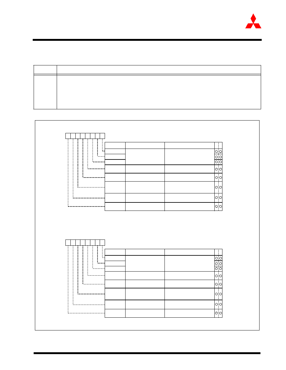
1-98
Mitsubishi microcomputers
M30240 Group
SINGLE-CHIP 16-BIT CMOS MICROCOMPUTER
Preliminary Specifications REV. E
Specifications in this manual are tentative and subject to change
UART0 through UART2
Figure 1.88: UARTi transmit/receive mode register in UART mode
Table 1.28:
Specifications of UART Mode (2)
Item
Specification
Select
function
� Sleep mode selection (UART0, UART1)
This mode is used to transfer data to and from one of multiple slave micro-computers
�Serial data logic switch (UART2)
This function is reversing logic value of transferring data. Start bit, parity bit and stop bit are not reversed.
�TxD, RxD I/O polarity switch
This function is reversing TxD port output and RxD port input. All I/O data level is reversed.
Symbol
Address
When reset
UiMR(i=0,1)
03A0
16
, 03A8
16
00
16
CKDIR
UARTi transmit / receive mode registers
Internal / external clock
select bit
STPS
PRY
PRYE
SLEP
0 : Internal clock
1 : External clock
Bit name
Function
Bit symbol
W
R
b7
b6
b5
b4
b3
b2
b1
b0
SMD0
SMD1
SMD2
Serial I/O mode select bit
b2 b1 b0
0 : One stop bit
1 : Two stop bits
0 : Parity disabled
1 : Parity enabled
0 : Sleep mode deselected
1 : Sleep mode selected
1 0 0 : Transfer data 7 bits long
1 0 1 : Transfer data 8 bits long
1 1 0 : Transfer data 9 bits long
Valid when bit 6 = "1"
0 : Odd parity
1 : Even parity
Stop bit length select bit
Odd / even parity
select bit
Parity enable bit
Sleep select bit
Symbol
Address
When reset
U2MR
0378
16
00
16
CKDIR
UART2 transmit / receive mode register
Internal / external clock
select bit
STPS
PRY
PRYE
IOPOL
0 : Internal clock
1 : External clock
Bit name
Function
Bit symbol
W
R
b7
b6
b5
b4
b3
b2
b1
b0
SMD0
SMD1
SMD2
Serial I/O mode select bit
b2 b1 b0
0 : One stop bit
1 : Two stop bits
0 : Parity disabled
1 : Parity enabled
0 : No reverse
1 : Reverse
1 0 0 : Transfer data 7 bits long
1 0 1 : Transfer data 8 bits long
1 1 0 : Transfer data 9 bits long
Valid when bit 6 = "1"
0 : Odd parity
1 : Even parity
Stop bit length select bit
Odd / even parity
select bit
Parity enable bit
TxD, RxD I/O polarity
reverse bit (Note)
Note: Usually set to "0".

1-99
Mitsubishi microcomputers
M30240 Group
SINGLE-CHIP 16-BIT CMOS MICROCOMPUTER
Preliminary Specifications REV. E
Specifications in this manual are tentative and subject to change
UART0 through UART2
Table 1.29 lists the functions of the input/output pins during UART mode. Note that for a period from
when the UARTi operation mode is selected to when transfer starts, the TxDi pin outputs a "H".
Figure 1.89 and Figure 1.90 show the typical UART mode transmit and receive timing diagrams.
Table 1.29:
Input/output pin functions in UART mode
Pin name
Function
Method of selection
TxDi
(P63, P67, P70)
Serial data
output
RxDi
(P62, P66, P71)
Serial data
input
Port P62, P66, and P71 direction register (bits 2 and 6 at address 03EE
16
bit 1
at address 03EF
16
)= "0"
(Can be used as an input port when performing transmission only.)
CLKi
(P61, P65, P72)
Programmable
I/O port
Internal/external clock select bit (bit 3 at address 03A0
16
, 03A8
16
, 0378
16
) = "0"
Transfer clock
input
Internal/external clock select bit (bit 3 at address 03A0
16
, 03A8
16
, 0378
16
) = "1"
Port P61, P65, and P72 direction register (bits 1 and 5 at address 03EE
16
, bit 2
at address 03EF
16
) = "0"
CTSi/RTSi
(P60,P64,P73)
CTS input
CTS/RTS disable bit (bit 4 at address 03A4
16
, 03AC
16
, 037C
16
) = "0"
CTS/RTS function select bit (bit 2 at address 03A4
16
, 03AC
16
, 037C
16
) = "0"
Port P60, P64 and P73 direction register (bits 0 and 4 at address 03EE
16
, bit 3
at address 03EF
16
) = "0"
RTS output
CTS/RTS disable bit (bit 4 at address 03A4
16
, 03AC
16
, 037C
16
) = "0"
CTS/RTS function select bit (bit 2 at address 03A4
16
, 03AC
16
, 037C
16
) = "1"
Programmable
I/O port
CTS/RTS disable bit (bit 4 at address 03A4
16
, 03AC
16
, 037C
16
) = "1"

1-100
Mitsubishi microcomputers
M30240 Group
SINGLE-CHIP 16-BIT CMOS MICROCOMPUTER
Preliminary Specifications REV. E
Specifications in this manual are tentative and subject to change
UART0 through UART2
Figure 1.89: Typical transmit timings in UART mode
Transmit enable
bit(TE)
Transmit buffer
empty flag(TI)
Transmit register
empty flag (TXEPT)
Start
bit
Parity
bit
TxDi
CTSi
The above timing applies to the following settings :
� Parity is enabled.
� One stop bit.
� CTS function is selected.
� Transmit interrupt cause select bit = "1".
"1"
"0"
"1"
"L"
"H"
"0"
"1"
Tc = 16 (n + 1) / fi or 16 (n + 1) / f
EXT
fi : frequency of BRGi count source (f
1
, f
8
, f
32
)
f
EXT
: frequency of BRGi count source (external clock)
n : value set to BRGi
Transmit interrupt
request bit (IR)
"0"
"1"
Cleared to "0" when interrupt request is accepted, or cleared by software
Transmit enable
bit(TE)
Transmit buffer
empty flag(TI)
TxDi
Transmit register
empty flag (TXEPT)
"0"
"1"
"0"
"1"
"0"
"1"
The above timing applies to the following settings :
� Parity is disabled.
� Two stop bits.
� CTS function is disabled.
� Transmit interrupt cause select bit = "0".
Transfer clock
Tc
Tc = 16 (n + 1) / fi or 16 (n + 1) / f
EXT
fi : frequency of BRGi count source (f
1
, f
8
, f
32
)
f
EXT
: frequency of BRGi count source (external clock)
n : value set to BRGi
Transmit interrupt
request bit (IR)
"0"
"1"
Shown in ( ) are bit symbols.
Shown in ( ) are bit symbols.
Tc
Transfer clock
D
0
D
1
D
2
D
3
D
4
D
5
D
6
D
7
ST
P
D
0
D
1
D
2
D
3
D
4
D
5
D
6
D
7
SP
ST
P
SP
D
0
D
1
ST
Stopped pulsing because transmit enable bit = "0"
Stop
bit
Transferred from UARTi transmit buffer register to UARTi transmit register
Start
bit
The transfer clock stops momentarily as CTS is "H" when the stop bit is checked.
The transfer clock starts as the transfer starts immediately CTS changes to "L".
Data is set in UARTi transmit buffer register
D
0
D
1
D
2
D
3
D
4
D
5
D
6
D
7
ST
SP
D
8
D
0
D
1
D
2
D
3
D
4
D
5
D
6
D
7
ST
D
8
D
0
D
1
ST
SPSP
Transferred from UARTi transmit buffer register to UARTi transmit register
Stop
bit
Stop
bit
Data is set in UARTi transmit buffer register.
"0"
SP
Cleared to "0" when interrupt request is accepted, or cleared by software
� Example of transmit timing when transfer data is 8 bits long (parity enabled, one stop bit)
� Example of receive timing when transfer data is 8 bits long (parity enabled, one stop bit)
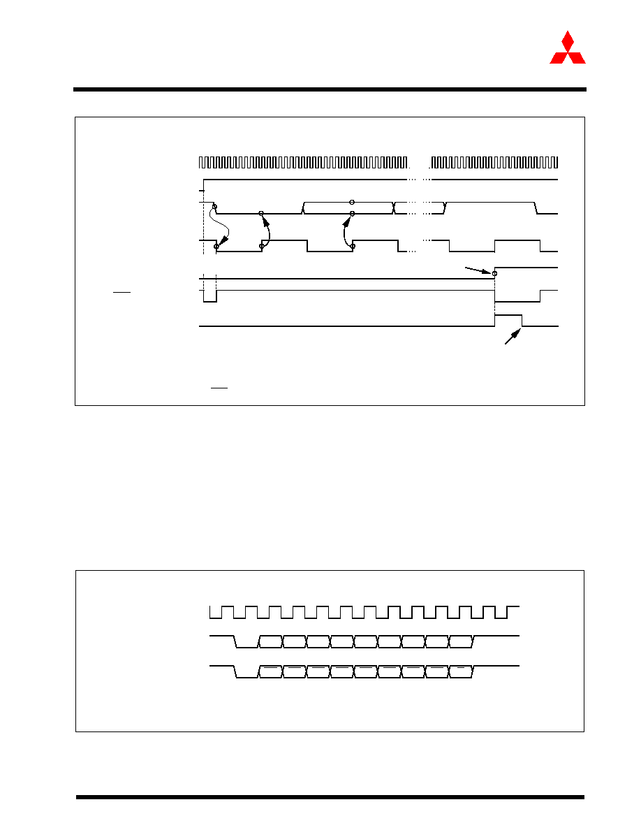
1-101
Mitsubishi microcomputers
M30240 Group
SINGLE-CHIP 16-BIT CMOS MICROCOMPUTER
Preliminary Specifications REV. E
Specifications in this manual are tentative and subject to change
UART0 through UART2
Figure 1.90: Typical receive timing in UART mode
2.23.2.1 Sleep mode (UART0, UART1)
This mode is used to transfer data between specific microcomputers among multiple microcomputers con-
nected using UARTi. The sleep mode is selected when the sleep select bit (bit 7 at addresses 03A0
16
,
03A8
16
) is set to "1" during reception. In this mode, the unit performs receive operation when the MSB of the
received data = "1" and does not perform receive operation when the MSB = "0".
2.23.2.2 Function for switching serial data logic (UART2)
When the data logic select bit (bit 6 of address 037D
16
) is assigned 1, data is inverted in writing to the trans-
mission buffer register or reading the reception buffer register. Figure 1.91 shows the example of timing for
switching serial data logic.
Figure 1.91: Timing for switching serial data logic
D
0
Start bit
Sampled "L"
Receive data taken in
BRGi count
source
Receive enable bit
RxDi
Transfer clock
Receive
complete flag
RTSi
Stop bit
"1"
"0"
"0"
"1"
"H"
"L"
The above timing applies to the following settings :
�Parity is disabled.
�One stop bit.
�RTS function is selected.
Receive interrupt
request bit
"0"
"1"
Transferred from UARTi receive register to
UARTi receive buffer register
Reception triggered when transfer clock
is generated by falling edge of start bit
D
7
D
1
Cleared to "0" when interrupt request is accepted, or cleared by software
Example of receive timing when transfer data is 8 bits long (parity disabled, one stop bit)
ST : Start bit
P : Even parity
SP : Stop bit
D0
D1
D2
D3
D4
D5
D6
D7
P
SP
ST
SP
ST
D3
D4
D5
D6
D7
P
D0
D1
D2
Transfer clock
TxD
2
(no reverse)
TxD
2
(reverse)
"H"
"L"
"H"
"L"
"H"
"L"
� When LSB first, parity enabled, one stop bit

1-102
Mitsubishi microcomputers
M30240 Group
SINGLE-CHIP 16-BIT CMOS MICROCOMPUTER
Preliminary Specifications REV. E
Specifications in this manual are tentative and subject to change
UART0 through UART2
2.23.2.3 TxD, RxD I/O polarity reverse function (UART2)
This function is to reverse TxD pin output and RxD pin input. The level of any data to be input or output (in-
cluding the start bit, stop bit(s), and parity bit) is reversed. Set this function to "0" (not to reverse) for usual use.
2.23.2.4 Bus collision detection function (UART2)
This function is to sample the output level of the TxD pin and the input level of the RxD pin at the rising edge
of the transfer clock; if their values are different, then an interrupt request occurs. Figure 1.92 shows the ex-
ample of detection timing of a buss collision (in UART mode).
Figure 1.92: Detection timing of a bus collision (in UART mode)
ST : Start bit
SP : Stop bit
ST
ST
SP
SP
Transfer clock
TxD
2
RxD
2
Bus collision detection
interrupt request signal
"H"
"L"
"H"
"L"
"H"
"L"
"1"
"0"
Bus collision detection
interrupt request bit
"1"
"0"
1-103
Mitsubishi microcomputers
M30240 Group
SINGLE-CHIP 16-BIT CMOS MICROCOMPUTER
Preliminary Specifications REV. E
Specifications in this manual are tentative and subject to change
UART0 through UART2
2.23.3 Clock-asynchronous serial I/O mode (compliant with the SIM interface)
The SIM interface is used for connecting the microcomputer with a memory card I/C or the like; adding
some extra settings in UART2 clock-asynchronous serial I/O mode allows the user to effect this func-
tion. Table 1.30 shows the specifications of clock-asynchronous serial I/O mode (compliant with the
SIM interface). Figure 1.93 shows the typical transmit/receive timing in UART mode.
Note 1: `n' denotes the value 00
16
to FF
16
that is set to the UARTi bit rate generator.
Note 2: fEXT is input from the CLK2 pin.
Note 3: If an overrun error occurs, the UART2 receive buffer will have the next data written in. Note also that the UARTi
receive interrupt request bit is not set to "1".
Table 1.30:
Specifications of clock-asynchronous serial I/O mode (compliant with the SIM interface)
Item
Specification
Transfer data
format
� Transfer data 8-bit UART mode (bit 2 through bit 0 of address 0378
16
= "1012")
� One stop bit (bit 4 of address 0378
16
= "0")
� With the direct format chosen
Set parity to "even" (bit 5 and bit 6 of address 0378
16
= "1" and "1" respectively)
Set data logic to "direct" (bit 6 of address 037D
16
= "0").
Set transfer format to LSB (bit 7 of address 037C
16
= "0").
� With the inverse format chosen
Set parity to "odd" (bit 5 and bit 6 of address 0378
16
= "0" and "1" respectively)
Set data logic to "inverse" (bit 6 of address 037D
16
= "1")
Set transfer format to MSB (bit 7 of address 037C
16
= "1")
Transfer clock
� With the internal clock chosen (bit 3 of address 0378
16
= "0"): fi / 16 (n + 1) (Note 1): fi=f1, f8, f32
� With an external clock chosen (bit 3 of address 0378
16
= "1"): fEXT / 16 (n+1) (Note 1) (Note 2)
Transmission /
reception control
� Disable the CTS and RTS function (bit 4 of address 037C
16
= "1")
Other settings
� The sleep mode select function is not available for UART2
� Set transmission interrupt factor to "transmission completed" (bit 4 of address 037D
16
= "1")
Transmission
start condition
� To start transmission, the following requirements must be met:
- Transmit enable bit (bit 0 of address 037D
16
) = "1"
- Transmit buffer empty flag (bit 1 of address 037D
16
) = "0"
Reception start
condition
� To start reception, the following requirements must be met:
- Reception enable bit (bit 2 of address 037D
16
) = "1"
- Detection of a start bit
� When transmitting
When data transmission from the UART2 transfer register is completed (bit 4 of address 037D
16
=
"1")
� When receiving
When data transfer from the UART2 receive register to the UART2 receive buffer register is
completed
Error detection
� Overrun error (see the specifications of clock-asynchronous serial I/O) (Note 3)
� Framing error (see the specifications of clock-asynchronous serial I/O)
� Parity error (see the specifications of clock-asynchronous serial I/O)
- On the reception side, an "L" level is output from the TxD2 pin by use of the parity error signal
output function (bit 7 of address 037D
16
= "1") when a parity error is detected
- On the transmission side, a parity error is detected by the level of input to the RxD2 pin when a
transmission interrupt occurs
� The error sum flag (see the specifications of clock-asynchronous serial I/O)

1-104
Mitsubishi microcomputers
M30240 Group
SINGLE-CHIP 16-BIT CMOS MICROCOMPUTER
Preliminary Specifications REV. E
Specifications in this manual are tentative and subject to change
UART0 through UART2
Figure 1.93: Typical transmit/receive timing in UART mode (compliant with the SIM interface)
Transmit enable
bit(TE)
Transmit buffer
empty flag(TI)
Transmit register
empty flag (TXEPT)
D
0
D
1
D
2
D
3
D
4
D
5
D
6
D
7
ST
P
Start
bit
Parity
bit
The above timing applies to the following settings :
� Parity is enabled.
� One stop bit.
� Transmit interrupt cause select bit = "1".
"0"
"1"
"0"
"1"
"0"
"1"
Tc = 16 (n + 1) / fi or 16 (n + 1) / f
EXT
fi : frequency of BRGi count source (f
1
, f
8
, f
32
)
f
EXT
: frequency of BRGi count source (external clock)
n : value set to BRGi
Transmit interrupt
request bit (IR)
"0"
"1"
D
0
D
1
D
2
D
3
D
4
D
5
D
6
D
7
ST
P
Shown in ( ) are bit symbols.
Tc
Transfer clock
SP
Stop
bit
Data is set in UARTi transmit buffer register
SP
A "L" level returns from TxD
2
due to
the occurrence of a parity error.
The level is detected by the
interrupt routine.
The level is
detected by the
interrupt routine.
Receive enable
bit (RE)
Receive complete
flag (RI)
D
0
D
1
D
2
D
3
D
4
D
5
D
6
D
7
ST
P
Start
bit
Parity
bit
TxD
2
The above timing applies to the following settings :
� Parity is enabled.
� One stop bit.
� Transmit interrupt cause select bit = "0".
"0"
"1"
"0"
"1"
Tc = 16 (n + 1) / fi or 16 (n + 1) / f
EXT
fi : frequency of BRGi count source (f
1
, f
8
, f
32
)
f
EXT
: frequency of BRGi count source (external clock)
n : value set to BRGi
Receive interrupt
request bit (IR)
"0"
"1"
D
0
D
1
D
2
D
3
D
4
D
5
D
6
D
7
ST
P
SP
Shown in ( ) are bit symbols.
Tc
Transfer clock
SP
Stop
bit
A "L" level returns from TxD
2
due to
the occurrence of a parity error.
RxD
2
Read to receive buffer
Read to receive buffer
D
0
D
1
D
2
D
3
D
4
D
5
D
6
D
7
ST
P
Signal conductor level
(Note 1)
D
0
D
1
D
2
D
3
D
4
D
5
D
6
D
7
ST
P
SP
SP
D
0
D
1
D
2
D
3
D
4
D
5
D
6
D
7
ST
P
D
0
D
1
D
2
D
3
D
4
D
5
D
6
D
7
ST
P
SP
SP
TxD
2
RxD
2
Signal conductor level
(Note 1)
Note: Equal in waveform because TxD
2
and RxD
2
are connected.
Transferred from UARTi transmit buffer register to UARTi transmit register
Cleared to "0" when interrupt request is accepted, or cleared by software
Cleared to "0" when interrupt request is accepted, or cleared by software
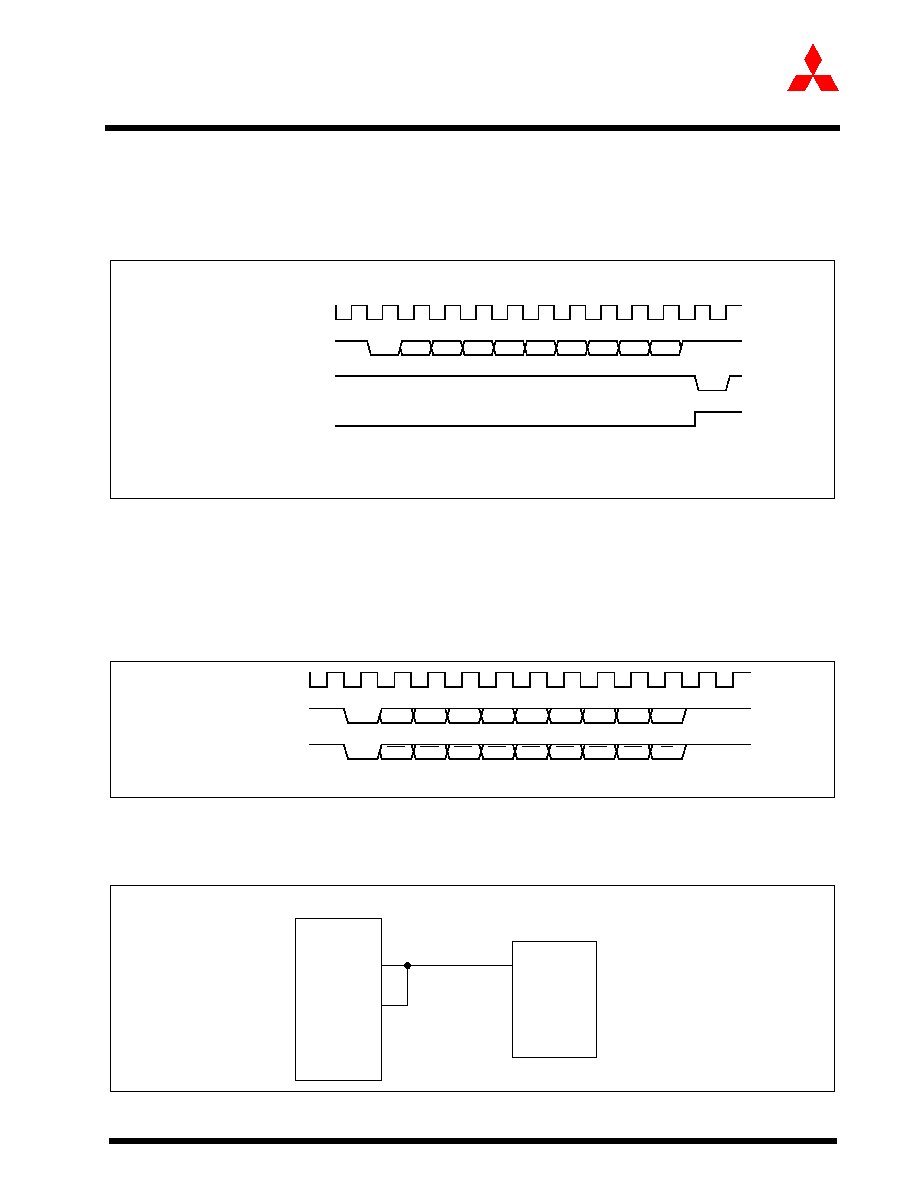
1-105
Mitsubishi microcomputers
M30240 Group
SINGLE-CHIP 16-BIT CMOS MICROCOMPUTER
Preliminary Specifications REV. E
Specifications in this manual are tentative and subject to change
UART0 through UART2
2.23.3.1 Function for outputting a parity error signal
With the error signal output enable bit (bit 7 of address 037D
16
) assigned "1", you can output an "L" level from
the TxD2 pin when a parity error is detected. In step with this function, the generation timing of a transmission
completion interrupt changes to the detection timing of a parity error signal. Figure 1.94 shows the output tim-
ing of the parity error signal.
Figure 1.94: Output timing of the parity error signal
2.23.3.2 Direct format/inverse format
Connecting the SIM card allows you to switch between direct format and inverse format. If you choose the
direct format, D0 data is output from TxD2. If you choose the inverse format, D7 data is inverted and output
from TxD2.
Figure 1.95 shows the SIM interface format.
Figure 1.95: SIM interface format
Figure 1.96 shows the example of connecting the SIM interface with TxD2 and RxD2.
Figure 1.96: Connecting the SIM interface
ST : Start bit
P : Even Parity
SP : Stop bit
D0
D1
D2
D3
D4
D5
D6
D7
P
SP
ST
Hi-Z
Transfer
clock
RxD
2
TxD
2
Receive
complete flag
"H"
"L"
"H"
"L"
"H"
"L"
"1"
� LSB first
"0"
P : Even parity
D0
D1
D2
D3
D4
D5
D6
D7
P
Transfer
clcck
TxD
2
(direct)
TxD
2
(inverse)
D7
D6
D5
D4
D3
D2
D1
D0
P
Microcomputer
SIM card
TxD
2
RxD
2
1-106
Mitsubishi microcomputers
M30240 Group
SINGLE-CHIP 16-BIT CMOS MICROCOMPUTER
Preliminary Specifications REV. E
Specifications in this manual are tentative and subject to change
A-D Converter
2.24 A-D Converter
The A-D converter consists of one 10-bit successive approximation A-D converter circuit with a
capacitive coupling amplifier. Pins P100 to P107 function as the analog signal input pins. The direction
registers of these pins for A-D conversion must therefore be set to input. The Vref connect bit (bit 5 at
address 03D7
16
) can be used to isolate the resistance ladder of the A-D converter from the reference
voltage input pin (VREF) when the A-D converter is not used. Doing so stops any current flowing into
the resistance ladder from VREF, reducing the power dissipation. When using the A-D converter, start
A-D conversion only after setting bit 5 of 03D7
16
to connect VREF.
The result of A-D conversion is stored in the A-D registers of the selected pins. When set to 10-bit
precision, the low 8 bits are stored in the even addresses and the high 2 bits in the odd addresses. When
set to 8-bit precision, the low 8 bits are stored in the even addresses.
Table 1.31 shows the performance of the A-D converter. Figure 1.97 shows the block diagram of the A-
D converter, and Figure 1.98 and Figure 1.99 show the A-D converter-related registers.
Table 1.31:
Performance of A-D Converter
Item
Performance
Method of A-D conversion
Successive approximation (capacitive coupling amplifier)
Analog input voltage (Note)
0V to AVCC (VCC)
Operating clock fAD
VCC = 5V
fAD/divide-by-2 or fAD/divide-by-4 or fAD, fAD=f(Xin)
Resolution
8-bit or 10-bit (selectable)
Absolute precision
VCC = 5V
� Without sample and hold function
3LSB
� With sample and hold function (8-bit resolution)
2LSB
� With sample and hold function (10-bit resolution)
3LSB
Operating modes
One-shot mode, repeat mode, single sweep mode, repeat sweep mode 0, and
repeat sweep mode 1
Analog input pins
8pins (AN0 to AN7)
A-D conversion start condition
�Software trigger
A-D conversion starts when the A-D conversion start flag changes to "1"
�External trigger (can be retriggered)
A-D conversion starts when the A-D conversion start flag is "1" and the AD
TRG
/P87
input changes from "H" to "L"
Conversion speed per pin
�Without sample and hold function
8-bit resolution: 49
AD cycles, 10-bit resolution: 59
AD cycles
� With sample and hold function
8-bit resolution: 28
AD cycles, 10-bit resolution: 33
AD cycles
Note Does not depend on use of sample and hold function.
1-107
Mitsubishi microcomputers
M30240 Group
SINGLE-CHIP 16-BIT CMOS MICROCOMPUTER
Preliminary Specifications REV. E
Specifications in this manual are tentative and subject to change
A-D Converter
Figure 1.97: Block diagram of A-D converter
1/2
AD
1/2
f
AD
A-D conversion rate
selection
(03C1
16
, 03C0
16
)
(03C3
16
, 03C2
16
)
(03C5
16
, 03C4
16
)
(03C7
16
, 03C6
16
)
(03C9
16
, 03C8
16
)
(03CB
16
, 03CA
16
)
(03CD
16
, 03CC
16
)
(03CF
16
, 03CE
16
)
CKS1=1
CKS0=0
A-D register 0(16)
A-D register 1(16)
A-D register 2(16)
A-D register 3(16)
A-D register 4(16)
A-D register 5(16)
A-D register 6(16)
A-D register 7(16)
Resistor ladder
Successive conversion register
AN
0
AN
1
AN
2
AN
3
AN
5
AN
6
AN
7
A-D control register 0 (address 03D6
16
)
A-D control register 1 (address 03D7
16
)
V
ref
V
IN
Data bus high-order
Data bus low-order
V
REF
AN
4
VCUT=0
AV
SS
VCUT=1
CKS0=1
CKS1=0
CH2,CH1,CH0=000
CH2,CH1,CH0=001
CH2,CH1,CH0=010
CH2,CH1,CH0=011
CH2,CH1,CH0=100
CH2,CH1,CH0=101
CH2,CH1,CH0=110
CH2,CH1,CH0=111
Decoder
Comparator
Addresses
1-108
Mitsubishi microcomputers
M30240 Group
SINGLE-CHIP 16-BIT CMOS MICROCOMPUTER
Preliminary Specifications REV. E
Specifications in this manual are tentative and subject to change
A-D Converter
Figure 1.98: A-D converter-related registers (1)
A-D control register 0 (Note 1)
Symbol
Address
When reset
ADCON0
03D6
16
00000XXX
2
b7
b6
b5
b4
b3
b2
b1
b0
Analog input pin select bit
0 0 0 : AN
0
is selected
0 0 1 : AN
1
is selected
0 1 0 : AN
2
is selected
0 1 1 : AN
3
is selected
1 0 0 : AN
4
is selected
1 0 1 : AN
5
is selected
1 1 0 : AN
6
is selected
1 1 1 : AN
7
is selected
(Note 2)
CH0
Bit symbol
Bit name
Function
CH1
CH2
A-D operation mode
select bit 0
0 0 : One-shot mode
0 1 : Repeat mode
1 0 : Single sweep mode
1 1 : Repeat sweep mode 0
Repeat sweep mode 1
(Note 2)
MD0
MD1
Trigger select bit
0 : Software trigger
1 : AD
TRG
trigger
TRG
ADST
A-D conversion start flag
0 : A-D conversion disabled
1 : A-D conversion started
Frequency select bit 0
0 : f
AD
/4 is selected
1 : f
AD
/2 is selected
CKS0
W
R
A-D control register 1 (Note)
Symbol
Address
When reset
ADCON1
03D7
16
00
16
Bit name
Function
Bit symbol
b7
b6
b5
b4
b3
b2
b1
b0
A-D sweep pin select bit
SCAN0
SCAN1
MD2
BITS
8/10-bit mode select bit
0 : 8-bit mode
1 : 10-bit mode
VCUT
Vref connect bit
A-D operation mode
select bit 1
0 : Any mode other than repeat sweep
mode 1
1 : Repeat sweep mode 1
0 : Vref not connected
1 : Vref connected
W
R
b2 b1 b0
b4 b3
When single sweep and repeat sweep
mode 0 are selected
0 0 : AN
0
, AN
1
(2 pins)
0 1 : AN
0
to AN
3
(4 pins)
1 0 : AN
0
to AN
5
(6 pins)
1 1 : AN
0
to AN
7
(8 pins)
b1 b0
When repeat sweep mode 1 is selected
0 0 : AN
0
(1 pin)
0 1 : AN
0
, AN
1
(2 pins)
1 0 : AN
0
to AN
2
(3 pins)
1 1 : AN
0
to AN
3
(4 pins)
b1 b0
Note 1: If the A-D control register is rewritten during A-D conversion, the conversion result is
indeterminate.
Note 2: When changing A-D operation mode, set analog input pin again.
Frequency select bit 1
0 : f
AD
/2 or f
AD
/4 is selected
1 : f
AD
is selected
CKS1
Note: If the A-D control register is rewritten during A-D conversion, the conversion result is
indeterminate.
Reserved bit
Always set to "0"
0 0
1-109
Mitsubishi microcomputers
M30240 Group
SINGLE-CHIP 16-BIT CMOS MICROCOMPUTER
Preliminary Specifications REV. E
Specifications in this manual are tentative and subject to change
A-D Converter
Figure 1.99: A-D converter-related registers (2)
A-D control register 2 (Note)
Symbol
Address
When reset
ADCON2
03D4
16
XXXXXXX0
2
b7
b6
b5
b4
b3
b2
b1
b0
A-D conversion method
select bit
0 : Without sample and hold
1 : With sample and hold
Bit symbol
Bit name
Function
R W
Note: If the A-D control register is rewritten during A-D conversion, the conversion
result is indeterminate.
Nothing is assigned.
These bits can neither be set nor reset. When read, their content is "0".
(JA 03 UM60)
A-D register i
Symbol
Address
When reset
ADi(i=0 to 7)
03C0
16
to 03CF
16
Indeterminate
Eight low-order bits of A-D conversion result
Function
R W
(b15)
b7
b7
b0
b0
(b8)
� During 10-bit mode
Two high-order bits of A-D conversion result
Nothing is assigned.
These bits can neither be set nor reset. When read, their
content is "0".
� During 8-bit mode
When read, the content is indeterminate
SMP
Reserved bit
Always set to "0"
0 0 0
1-110
Mitsubishi microcomputers
M30240 Group
SINGLE-CHIP 16-BIT CMOS MICROCOMPUTER
Preliminary Specifications REV. E
Specifications in this manual are tentative and subject to change
A-D Converter
2.24.1 One-shot mode
In one-shot mode, the pin selected using the analog input pin select bit is used for one-shot A-D con-
version.Table 1.32 shows the specifications of one-shot mode. Figure 1.100 shows the A-D control
register in one-shot mode.
Figure 1.100: A-D conversion register in one-shot mode
Table 1.32:
One-shot mode specification
Item
Specification
Function
The pin selected by the analog input pin select bit is used for one A-D conversion
Start condition
Writing "1" to A-D conversion start flag
Stop condition
�End of A-D conversion (A-D conversion start flag changes to "0", except
when external trigger is selected)
�Writing "0" to A-D conversion start flag
Interrupt request generation
timing
End of A-D conversion
Input pin
One of AN0 to AN7, as selected
Reading of result of A-D converter
Read A-D register corresponding to selected pin
A-D control register 0 (Note 1)
Symbol
Address
When reset
ADCON0
03D6
16
00000XXX
2
b7
b6
b5
b4
b3
b2
b1
b0
Analog input pin select
bit
Bit symbol
Bit name
Function
CH1
CH2
A-D operation mode
select bit 0
MD0
MD1
Trigger select bit
0 : Software trigger
1 : AD
TRG
trigger
TRG
ADST
A-D conversion start flag
0 : A-D conversion disabled
1 : A-D conversion started
Frequency select bit 0
0: f
AD
/4 is selected
1: f
AD
/2 is selected
CKS0
W
R
0
0
A-D control register 1 (Note)
Symbol
Address
When reset
ADCON1
03D7
16
00
16
Bit name
Function
Bit symbol
b7
b6
b5
b4
b3
b2
b1
b0
A-D sweep pin
select bit
SCAN0
SCAN1
MD2
BITS
8/10-bit mode select bit
0 : 8-bit mode
1 : 10-bit mode
VCUT
Vref connect bit
A-D operation mode
select bit 1
0 : Any mode other than repeat sweep
mode 1
1 : Vref connected
W
R
Invalid in one-shot mode
0
0 0 0 : AN
0
is selected
0 0 1 : AN
1
is selected
0 1 0 : AN
2
is selected
0 1 1 : AN
3
is selected
1 0 0 : AN
4
is selected
1 0 1 : AN
5
is selected
1 1 0 : AN
6
is selected
1 1 1 : AN
7
is selected
(Note 2)
b2 b1 b0
0 0 : One-shot mode
(Note 2)
b4 b3
CH0
1
Note 1: If the A-D control register is rewritten during A-D conversion, the conversion
result is indeterminate.
Note 2: When changing A-D operation mode, set analog input pin again.
Frequency select bit1
0 : f
AD
/2 or f
AD
/4 is selected
1 : f
AD
is selected
CKS1
Note: If the A-D control register is rewritten during A-D conversion, the conversion
result is indeterminate.
Reserved bit
Always set to "0"
0 0
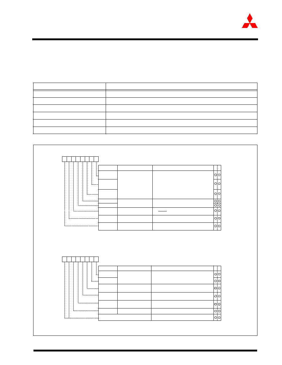
1-111
Mitsubishi microcomputers
M30240 Group
SINGLE-CHIP 16-BIT CMOS MICROCOMPUTER
Preliminary Specifications REV. E
Specifications in this manual are tentative and subject to change
A-D Converter
2.24.2 Repeat mode
In repeat mode, the pin selected using the analog input pin select bit is used for repeated A-D conver-
sion. Table 1.33 shows the specifications of repeat mode. Figure 1.101 shows the A-D control register
in repeat mode.
Figure 1.101: A-D conversion register in repeat mode
Table 1.33:
Repeat sweep mode 0 specifications
Item
Specification
Function
The pin selected by the analog input pin select bit is used for repeated A-D conversion
Star condition
Writing "1" to A-D conversion start flag
Stop condition
Writing "0" to A-D conversion start flag
Interrupt request generation timing
None generated
Input pin
One of AN0 to AN7, as selected
Reading of result of A-D converter
Read A-D register corresponding to selected pin
A-D control register 0 (Note 1)
Symbol
Address
When reset
ADCON0
03D6
16
00000XXX
2
b7
b6
b5
b4
b3
b2
b1
b0
Analog input pin
select bit
CH0
Bit symbol
Bit name
Function
CH1
CH2
A-D operation mode
select bit 0
MD0
MD1
Trigger select bit
0 : Software trigger
1 : AD
TRG
trigger
TRG
ADST
A-D conversion start flag
0 : A-D conversion disabled
1 : A-D conversion started
Frequency select bit 0
0 : f
AD
/4 is selected
1 : f
AD
/2 is selected
CKS0
W
R
A-D control register 1 (Note)
Symbol
Address
When reset
ADCON1
03D7
16
00
16
Bit name
Function
Bit symbol
b7
b6
b5
b4
b3
b2
b1
b0
A-D sweep pin
select bit
SCAN0
SCAN1
MD2
BITS
8/10-bit mode select bit
0 : 8-bit mode
1 : 10-bit mode
VCUT
Vref connect bit
A-D operation mode
select bit 1
1 : Vref connected
W
R
0
1
Invalid in repeat mode
0
0 0 0 : AN
0
is selected
0 0 1 : AN
1
is selected
0 1 0 : AN
2
is selected
0 1 1 : AN
3
is selected
1 0 0 : AN
4
is selected
1 0 1 : AN
5
is selected
1 1 0 : AN
6
is selected
1 1 1 : AN
7
is selected
(Note 2)
b2 b1 b0
0 1 : Repeat mode
(Note 2)
b4 b3
1
Note 1: If the A-D control register is rewritten during A-D conversion, the conversion
result is indeterminate.
Note 2: When changing A-D operation mode, set analog input pin again.
Frequency select bit 1
0 : f
AD
/2 or f
AD
/4 is selected
1 : f
AD
is selected
CKS1
0 : Any mode other than repeat sweep mode 1
Note: If the A-D control register is rewritten during A-D conversion, the conversion
result is indeterminate.
Reserved bit
Always set to "0"
0 0
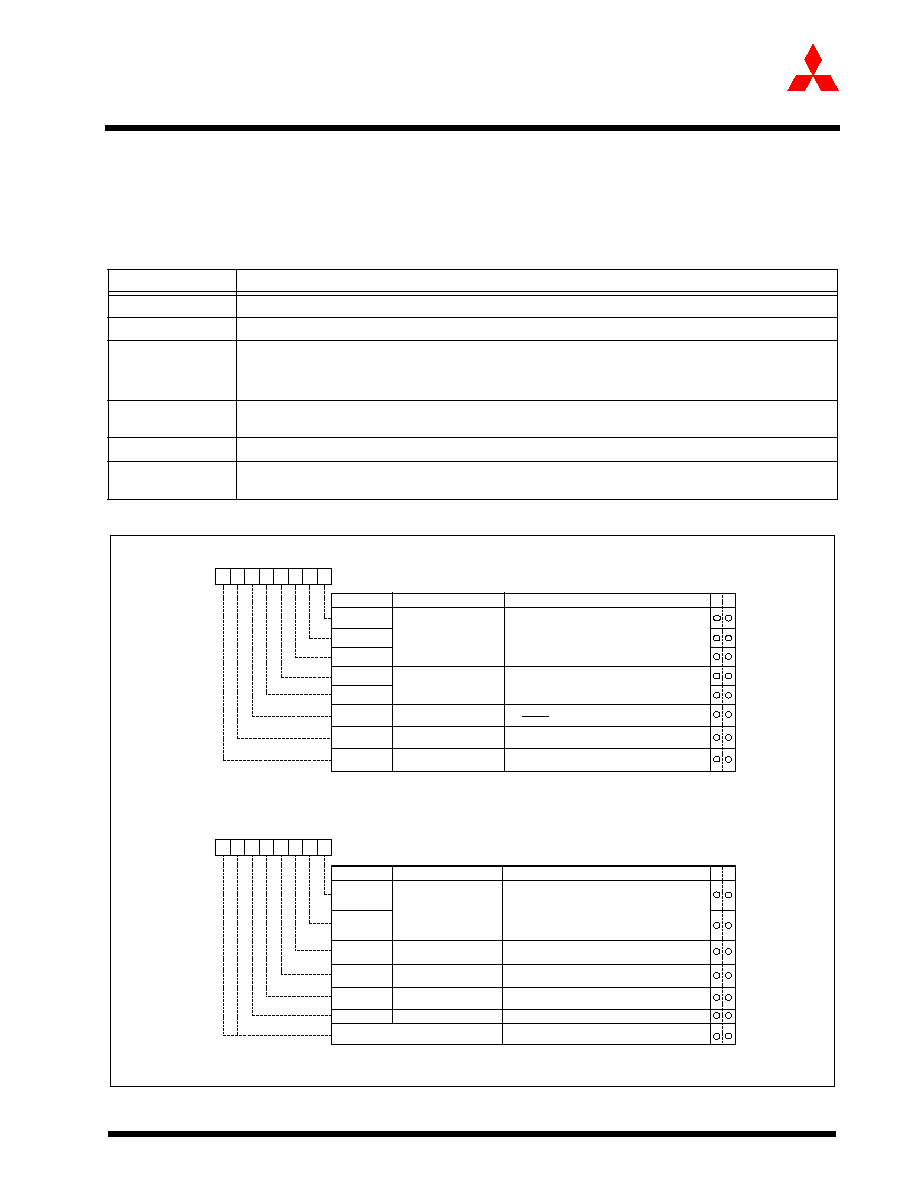
1-112
Mitsubishi microcomputers
M30240 Group
SINGLE-CHIP 16-BIT CMOS MICROCOMPUTER
Preliminary Specifications REV. E
Specifications in this manual are tentative and subject to change
A-D Converter
2.24.3 Single sweep mode
In single sweep mode, the pins selected using the A-D sweep pin select bit are used for one-by-one
A-D conversion. Table 1.34 shows the specifications of single sweep mode. Figure 1.102 shows the
A-D control register in single sweep mode.
Figure 1.102: A-D conversion register in single sweep mode
Table 1.34:
Single sweep mode specification
Item
Specification
Function
The pins selected by the A-D sweep pin select bit are used for one-by-one A-D conversion
Start condition
Writing "1" to A-D converter start flag
Stop condition
�End of A-D conversion (A-D conversion start flag changes to "0", except when external trigger is
selected)
�Writing "0" to A-D conversion start flag
Interrupt request
generation timing
End of A-D conversion
Input pin
AN0 and AN1 (2 pins), AN0 to AN3 (4 pins), AN0 to AN5 (6 pins), or AN0 to AN7 (8 pins)
Reading of result
of A-D converter
Read A-D register corresponding to selected pin
A-D control register 0 (Note)
Symbol
Address
When reset
ADCON0
03D6
16
00000XXX
2
b7
b6
b5
b4
b3
b2
b1
b0
Analog input pin
select bit
CH0
Bit symbol
Bit name
Function
CH1
CH2
A-D operation mode
select bit 0
1 0 : Single sweep mode
MD0
MD1
Trigger select bit
0 : Software trigger
1 : AD
TRG
trigger
TRG
ADST
A-D conversion start flag
0 : A-D conversion disabled
1 : A-D conversion started
Frequency select bit 0
0 : f
AD
/4 is selected
1 : f
AD
/2 is selected
CKS0
W
R
A-D control register 1 (Note)
Symbol
Address
When reset
ADCON1
03D7
16
00
16
Bit name
Function
Bit symbol
b7
b6
b5
b4
b3
b2
b1
b0
A-D sweep pin select bit
SCAN0
SCAN1
MD2
BITS
8/10-bit mode select bit
0 : 8-bit mode
1 : 10-bit mode
VCUT
Vref connect bit
0 : Any mode other than repeat sweep mode 1
A-D operation mode
select bit 1
1 : Vref connected
W
R
1
0
Invalid in single sweep mode
0
Note : If the A-D control register is rewritten during A-D conversion, the conversion result
is indeterminate.
b4 b3
When single sweep and repeat sweep mode 0
are selected
0 0 : AN
0
, AN
1
(2 pins)
0 1 : AN
0
to AN
3
(4 pins)
1 0 : AN
0
to AN
5
(6 pins)
1 1 : AN
0
to AN
7
(8 pins)
b1 b0
1
Note: If the A-D control register is rewritten during A-D conversion, the conversion result
is indeterminate.
Frequency select bit 1
0 : f
AD
/2 or f
AD
/4 is selected
1 : f
AD
is selected
CKS1
Reserved bit
Always set to "0"
0 0
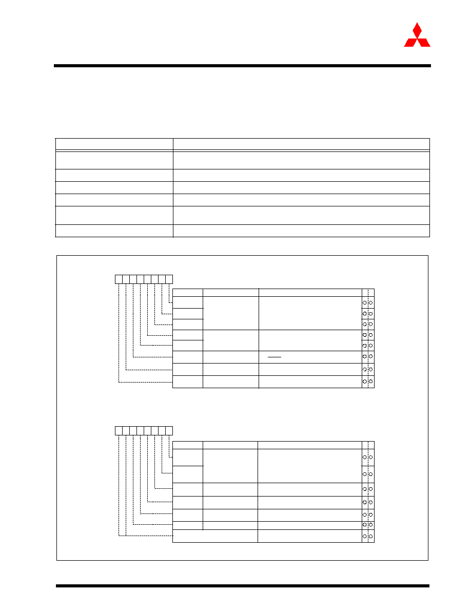
1-113
Mitsubishi microcomputers
M30240 Group
SINGLE-CHIP 16-BIT CMOS MICROCOMPUTER
Preliminary Specifications REV. E
Specifications in this manual are tentative and subject to change
A-D Converter
2.24.4 Repeat sweep mode 0
In repeat sweep mode 0, the pins selected using the A-D sweep pin select bit are used for repeat
sweep A-D conversion. Table 1.35 shows the specifications of repeat sweep mode 0. Figure 1.103
shows the A-D control register in repeat sweep mode 0.
Figure 1.103: A-D conversion register in repeat sweep mode 0
Table 1.35:
Repeat sweep mode 0 specifications
Item
Specification
Function
The pins selected by the A-D sweep pin select bit are used for repeat sweep A-D
conversion
Start condition
Writing "1" to A-D conversion start flag
Stop condition
Writing "0" to A-D conversion start flag
Interrupt request generation timing
None generated
Input pin
AN0 and AN1 (2 pins), AN0 to AN3 (4 pins), AN0 to AN5 (6 pins), or AN0 to AN7
(8 pins)
Reading of result of A-D converter
Read A-D register corresponding to selected pin (at any time)
A-D control register 0 (Note)
Symbol
Address
When reset
ADCON0
03D6
16
00000XXX
2
b7
b6
b5
b4
b3
b2
b1
b0
Analog input pin
select bit
CH0
Bit symbol
Bit name
Function
CH1
CH2
A-D operation mode
select bit 0
1 1 : Repeat sweep mode 0
MD0
MD1
Trigger select bit
0 : Software trigger
1 : AD
TRG
trigger
TRG
ADST
A-D conversion start flag
0 : A-D conversion disabled
1 : A-D conversion started
Frequency select bit 0
0 : f
AD
/4 is selected
1 : f
AD
/2 is selected
CKS0
W
R
A-D control register 1 (Note)
Symbol
Address
When reset
ADCON1
03D7
16
00
16
Bit name
Function
Bit symbol
b7
b6
b5
b4
b3
b2
b1
b0
A-D sweep pin select bit
SCAN0
SCAN1
MD2
BITS
8/10-bit mode select bit
0 : 8-bit mode
1 : 10-bit mode
VCUT
Vref connect bit
0 : Any mode other than repeat sweep mode 1
A-D operation mode
select bit 1
1 : Vref connected
W
R
1 1
Invalid in repeat sweep mode 0
0
Note: If the A-D control register is rewritten during A-D conversion, the conversion result
is indeterminate.
b4 b3
When single sweep and repeat sweep mode 0
are selected
0 0 : AN
0
, AN
1
(2 pins)
0 1 : AN
0
to AN
3
(4 pins)
1 0 : AN
0
to AN
5
(6 pins)
1 1 : AN
0
to AN
7
(8 pins)
b1 b0
1
Note: If the A-D control register is rewritten during A-D conversion, the conversion result
is indeterminate.
Frequency select bit 1
0 : f
AD
/2 or f
AD
/4 is selected
1 : f
AD
is selected
CKS1
Reserved bit
Always set to "0"
0 0

1-114
Mitsubishi microcomputers
M30240 Group
SINGLE-CHIP 16-BIT CMOS MICROCOMPUTER
Preliminary Specifications REV. E
Specifications in this manual are tentative and subject to change
A-D Converter
2.24.5 Repeat sweep mode 1
In repeat sweep mode 1, all pins are used for A-D conversion with emphasis on the pin or pins select-
ed using the A-D sweep pin select bit. Table 1.36 shows the specifications of repeat sweep mode 1.
Figure 1.104 show the A-D control in repeat sweep mode 1.
Table 1.36:
Repeat sweep mode 1 specification
Figure 1.104: A-D conversion register in repeat sweep mode 1
Item
Specification
Function
All pins perform repeat sweep A-D conversion, with emphasis on the pin or
pins selected by the A-D sweep pin select bit
Example: AN0 selected AN0 AN1 AN0 AN2 AN0 AN3, etc.
Start condition
Writing "1" to A-D conversion start flag
Stop condition
Writing "0" to A-D conversion start flag
Interrupt request generation timing
None generated
Input pin
AN0 (1 pin), AN0 and AN1 (2 pins), AN0 to AN2 (3 pins), AN0 to AN3 (4 pins)
Reading of result of A-D converter
Read A-D register corresponding to selected pin (at any time)
A-D control register 0 (Note)
Symbol
Address
When reset
ADCON0
03D6
16
00000XXX
2
b7
b6
b5
b4
b3
b2
b1
b0
Analog input pin
select bit
CH0
Bit symbol
Bit name
Function
CH1
CH2
A-D operation mode
select bit 0
1 1 : Repeat sweep mode 1
MD0
MD1
Trigger select bit
0 : Software trigger
1 : AD
TRG
trigger
TRG
ADST
A-D conversion start flag
0 : A-D conversion disabled
1 : A-D conversion started
Frequency select bit 0
0 : f
AD
/4 is selected
1 : f
AD
/2 is selected
CKS0
W
R
A-D control register 1 (Note)
Symbol
Address
When reset
ADCON1
03D7
16
00
16
Bit name
Function
Bit symbol
b7
b6
b5
b4
b3
b2
b1
b0
A-D sweep pin select bit
SCAN0
SCAN1
MD2
BITS
8/10-bit mode select bit
0 : 8-bit mode
1 : 10-bit mode
VCUT
Vref connect bit
1 : Repeat sweep mode 1
A-D operation mode
select bit 1
1 : Vref connected
W
R
1 1
Invalid in repeat sweep mode 1
1
Note: If the A-D control register is rewritten during A-D conversion, the conversion result
is indeterminate.
b4 b3
When repeat sweep mode 1 is selected
0 0 : AN
0
(1 pin)
0 1 : AN
0
, AN
1
(2 pins)
1 0 : AN
0
to AN
2
(3 pins)
1 1 : AN
0
to AN
3
(4 pins)
b1 b0
1
Note: If the A-D control register is rewritten during A-D conversion, the conversion result
is indeterminate.
Frequency select bit 1
0 : f
AD
/2 or f
AD
/4 is selected
1 : f
AD
is selected
CKS1
0 0
Reserved bit
Always set to "0
"

1-115
Mitsubishi microcomputers
M30240 Group
SINGLE-CHIP 16-BIT CMOS MICROCOMPUTER
Preliminary Specifications REV. E
Specifications in this manual are tentative and subject to change
A-D Converter
2.24.6 Sample and hold
Sample and hold is selected by setting bit 0 of the A-D control register 2 (address 03D4
16
) to "1". When
sample and hold is selected, the rate of conversion of each pin increases. As a result, a 28
AD cycle
is achieved with 8-bit resolution and 33
AD with 10-bit resolution. Sample and hold can be selected
in all modes. However, in all modes, be sure to specify before starting A-D conversion whether sample
and hold is to be used.
1-116
Mitsubishi microcomputers
M30240 Group
SINGLE-CHIP 16-BIT CMOS MICROCOMPUTER
Preliminary Specifications REV. E
Specifications in this manual are tentative and subject to change
CRC Calculation Circuit
2.25 CRC Calculation Circuit
The Cyclic Redundancy Check (CRC) calculation circuit detects an error in data blocks. The
microcomputer uses a generator polynomial of CRC_CCITT (X16 + X12 + X5 + 1) to generate CRC
code.
The CRC code is a 16-bit code generated for a block of a given data length in multiples of 8 bits. The
CRC code is set in a CRC data register each time one byte of data is transferred to a CRC input register
after writing an initial value into the CRC data register. Generation of CRC code for one byte of data is
completed in two machine cycles.
Figure 1.105 shows the block diagram of the CRC circuit. Figure 1.106 shows the CRC-related registers.
Figure 1.105: Block diagram of CRC circuit
Figure 1.106: CRC-related registers
Eight low-order bits
Eight high-order bits
Data bus high-order bits
Data bus low-order bits
CRC data register (16)
CRC input register (8)
CRC code generating circuit
x
16
+ x
12
+ x
5
+ 1
(Addresses 03BD
16
, 03BC
16
)
(Address 03BE
16
)
Symbol
Address
When reset
CRCD
03BD
16
, 03BC
16
Indeterminate
b7
b0 b7
b0
(b15)
(b8)
CRC data register
W
R
CRC calculation result output register
Function
Values that
can be set
0000
16
to FFFF
16
Symbo
Address
When reset
CRCIN
03BE
16
Indeterminate
b7
b0
CRC input register
W
R
Data input register
Function
Values that
can be set
00
16
to FF
16

1-117
Mitsubishi microcomputers
M30240 Group
SINGLE-CHIP 16-BIT CMOS MICROCOMPUTER
Preliminary Specifications REV. E
Specifications in this manual are tentative and subject to change
Programmable I/O Ports
2.26 Programmable I/O Ports
There are 63 programmable I/O ports: P0 to P3, P6 to P8 (excluding P85), and P10. Each port can be
set independently for input or output using the direction register. A pull-up resistance for each block of
4 ports can be set. P85 is an input-only port and has no built-in pull-up resistance.
Figure 1.107, Figure 1.108 and Figure 1.109 show the programmable I/O ports.
Each pin functions as a programmable I/O port and as the I/O for the built-in peripheral devices.
To use the pins as the inputs for the built-in peripheral devices, set the direction register of each pin to
input mode. When the pins are used as the outputs for the built-in peripheral devices, they function as
outputs regardless of the contents of the direction registers. Unused I/O pins can be terminated as
shown in Figure 1.114 and Table 1.37 .
2.26.1 Direction registers
Figure 1.110 shows the direction registers.
These registers are used to choose the direction of the programmable I/O ports. Each bit in these reg-
isters corresponds one for one to each I/O pin.
Note: There is no direction register bit for P85.
2.26.2 Port registers
Figure 1.111 shows the port registers.
These registers are used to write and read data for input and output to and from an external device.
A port register consists of a port latch to hold output data and a circuit to read the status of a pin. Each
bit in port registers corresponds one for one to each I/O pin.
2.26.3 Pull-up control registers
Figure 1.112 shows the pull-up control registers.The pull-up control register can be set to apply a pull-
up resistance to each block of 4 ports. When ports are set to have a pull-up resistance, the pull-up
resistance is connected only when the direction register is set for input.
2.26.4 High drive capacity registers
Figure 1.113 shows the Port 2 and PWM drive capacity register. Port 2 can be configured to drive an
LED by increasing the drive strength of the corresponding bit's N-channel transistor. Each Timer out-
put (TA0OUT~TA4OUT) can be configured for high-drive capability by increasing the drive strength of
the corresponding bits.

1-118
Mitsubishi microcomputers
M30240 Group
SINGLE-CHIP 16-BIT CMOS MICROCOMPUTER
Preliminary Specifications REV. E
Specifications in this manual are tentative and subject to change
Programmable I/O Ports
Figure 1.107: Programmable I/O ports (1)
P3
0
to P3
6
Data bus
Direction register
Pull-up selection
Port latch
Input to respective peripheral functions
P0
0
to P0
7
P1
0
to P1
7
P62, P66, P71,
P73,P75, P77,
P81, P82,
P84, P87
Data bus
Pull-up selection
Port latch
Direction register
Data bus
Pull-up selection
output
"1"
Input to respective peripheral functions
Direction register
Port latch
Drive capacity control register
P70, P72,
P74, P76,
P80
P2
0
to P2
7
Data bus
Direction register
Pull-up selection
Port latch
Drive capacity control register
1-119
Mitsubishi microcomputers
M30240 Group
SINGLE-CHIP 16-BIT CMOS MICROCOMPUTER
Preliminary Specifications REV. E
Specifications in this manual are tentative and subject to change
Programmable I/O Ports
Figure 1.108: Programmable I/O ports (2)
P10
0
to P10
7
Data bus
Pull-up selection
Analog input
Direction register
Port latch
P3
7
P6
3
, P6
7
P8
6
Data bus
Pull-up selection
"1"
output
Direction register
Port latch
Data bus
Pull-up selection
output
"1"
Input to respective peripheral functions
Direction register
Port latch
P6
0,
P6
1,
P6
4
, P6
5
P8
5
Data bus
NMI interrupt input

1-120
Mitsubishi microcomputers
M30240 Group
SINGLE-CHIP 16-BIT CMOS MICROCOMPUTER
Preliminary Specifications REV. E
Specifications in this manual are tentative and subject to change
Programmable I/O Ports
Figure 1.109: Programmable I/O Ports (3)
Figure 1.110: Direction register
BYTE Input
CNVss Input
RESET Input
BYTE
CNVss
RESET
Note: Do not apply a voltage higher than Vcc to each port
Port Pi direction register
Symbol
Address
When reset
PDi (i = 0 to 3,6,7,10)
03E2
16
, 03E3
16
, 03E6
16
, 03E7
16
,
00
16
03EE
16,
03EF
16
, 03F6
16
Bit name
Function
Bit symbol
W
R
b7
b6
b5
b4
b3
b2
b1
b0
PDi_0
Port Pi
0
direction register
PDi_1
Port Pi
1
direction register
PDi_2
Port Pi
2
direction register
PDi_3
Port Pi
3
direction register
PDi_4
Port Pi
4
direction register
PDi_5
Port Pi
5
direction register
PDi_6
Port Pi
6
direction register
PDi_7
Port Pi
7
direction register
0 : Input mode
(Functions as an input port)
1 : Output mode
(Functions as an output port)
(i = 0 to 3,6,7,10)
Port P8 direction register
Symbol
Address
When reset
PD8
03F2
16
00X00000
2
Bit name
Function
Bit symbol
W
R
b7
b6
b5
b4
b3
b2
b1
b0
PD8_0
Port P8
0
direction register
PD8_1
Port P8
1
direction register
PD8_2
Port P8
2
direction register
PD8_3
Port P8
3
direction register
PD8_4
Port P8
4
direction register
Nothing is assigned.
This bit can either be set nor reset. When read, its content is indeterminate.
PD8_6
Port P8
6
direction register
PD8_7
Port P8
7
direction register
0 : Input mode
(Functions as an input port)
1 : Output mode
(Functions as an output port)
0 : Input mode
(Functions as an input port)
1 : Output mode
(Functions as an output port)

1-121
Mitsubishi microcomputers
M30240 Group
SINGLE-CHIP 16-BIT CMOS MICROCOMPUTER
Preliminary Specifications REV. E
Specifications in this manual are tentative and subject to change
Programmable I/O Ports
Figure 1.111: Port register
Figure 1.112: Pull-up control register
Port Pi register
Symbol
Address
When reset
Pi (i = 0 to 3,6,7,10)
03E0
16
, 03E1
16
, 03E4
16
, 03E5
16
Indeterminate
03EC
16
, 03ED
16
, 03F4
16
Indeterminate
Bit name
Function
Bit symbol
W
R
b7
b6
b5
b4
b3
b2
b1
b0
Pi_0
Port Pi
0
register
Pi_1
Port Pi
1
register
Pi_2
Port Pi
2
register
Pi_3
Port Pi
3
register
Pi_4
Port Pi
4
register
Pi_5
Port Pi
5
register
Pi_6
Port Pi
6
register
Pi_7
Port Pi
7
register
Data is input and output to and from
each pin by reading and writing to
and from each corresponding bit
0 : "L" level data
1 : "H" level data
(i = 0 to 3,6,7,10)
Port P8 register
Symbol
Address
When reset
P8
03F0
16
Indeterminate
Bit name
Function
Bit symbol
W
R
b7
b6
b5
b4
b3
b2
b1
b0
P8_0
Port P8
0
register
P8_1
Port P8
1
register
P8_2
Port P8
2
register
P8_3
Port P8
3
register
P8_4
Port P8
4
register
P8_5
Port P8
5
register
P8_6
Port P8
6
register
P8_7
Port P8
7
register
Data is input and output to and from
each pin by reading and writing to
and from each corresponding bit
(except for P8
5
)
0 : "L" level data
1 : "H" level data
Pull-up control register 0
Symbol
Address
When reset
PUR0
03FC
16
00
16
Bit name
Function
Bit symbol
W
R
b7
b6
b5
b4
b3
b2
b1
b0
PU00
P0
0
to P0
3
pull-up
PU01
P0
4
to P0
7
pull-up
PU02
P1
0
to P1
3
pull-up
PU03
P1
4
to P1
7
pull-up
PU04
P2
0
to P2
3
pull-up
PU05
P2
4
to P2
7
pull-up
PU06
P3
0
to P3
3
pull-up
PU07
P3
4
to P3
7
pull-up
The corresponding port is pulled
high with a pull-up resistor
0 : Not pulled high
1 : Pulled high
Pull-up control register 1
Symbol
Address
When reset
PUR1
03FD
16
00
16
Bit name
Function
Bit symbol
W
R
b7
b6
b5
b4
b3
b2
b1
b0
PU10
P6
0
to P6
3
pull-up
PU11
P6
4
to P6
7
pull-up
PU12
P7
0
to P7
3
pull-up
PU13
P7
4
to P7
7
pull-up
PU14
P8
0
to P8
3
pull-up
PU15
P8
4,
P8
6,
P8
7
pull-up
PU16
P10
0
to P10
3
pull-up
PU17
P10
4
to P10
7
pull-up
The corresponding port is pulled
high with a pull-up resistor
0 : Not pulled high
1 : Pulled high
1-122
Mitsubishi microcomputers
M30240 Group
SINGLE-CHIP 16-BIT CMOS MICROCOMPUTER
Preliminary Specifications REV. E
Specifications in this manual are tentative and subject to change
Programmable I/O Ports
Figure 1.113: Port 2 and Timer A Output drive capacity registers
Port 2 Drive Capacity Register
Symbol
Address
When reset
P2DR
03FA
16
00
16
Bit name
Function
Bit symbol
W
R
b7
b6
b5
b4
b3
b2
b1
b0
P2DR0
P2
0
LED drive capacity
P2DR1
P2
1
LED drive capacity
P2DR2
P2
2
LED drive capacity
P2DR3
P2
3
LED drive capacity
P2DR4
P2
4
LED drive capacity
P2DR5
P2
5
LED drive capacity
P2DR6
P2
6
LED drive capacity
P2DR7
P2
7
LED drive capacity
The N-channel high-drive capacity
is activated for the corresponding
bit.
0 : Normal drive
1 : N-channel high drive
Timer A Output drive capacity register
Symbol
Address
When reset
TADR
03FB
16
00
16
Bit name
Function
Bit symbol
W
R
b7
b6
b5
b4
b3
b2
b1
b0
TADR0
TA0OUT drive capacity
TADR1
TA1OUT drive capacity
TADR2
TA2OUT drive capacity
TADR3
TA3OUT drive capacity
TADR4
TA4OUT drive capacity
High-drive capacity is activated for
the corresponding TAiOUT pin.
0 : Normal drive
1 : High drive
Nothing is assigned. These bits can neither be
set nor reset. When read, their content is 0.
_ _

1-123
Mitsubishi microcomputers
M30240 Group
SINGLE-CHIP 16-BIT CMOS MICROCOMPUTER
Preliminary Specifications REV. E
Specifications in this manual are tentative and subject to change
Programmable I/O Ports
Figure 1.114: Example connection unused pins
Table 1.37:
Example connection of unused pins in single-chip mode
Pin name
Connection
Ports P0 to P3, P6 to P8, P10
(excluding P85)
After setting for input mode, connect every pin to Vss or Vcc via a resistor; or
after setting for output mode, leave these pins open
Xout
Open
NMI
Connect via resistor to Vcc (pull-up)
AVcc
Connect to Vcc
Avss, Vref, BYTE
Connect to Vss
USB D+, USB D-
Open
ExtCap
Connect to Vcc (when DC-DC converter is disabled)
Connect to Vss via cap (when DC-DC converter is enabled and using the
ATTACH function)
SOF
Open
ATTACH
Open
Port P0 to P3, P6-P8, P10
(except P8
5
)
(Input mode)
�
�
�
(Input mode)
(Output mode)
USB D+
USB D-
Microcomputer
AV
CC
ExtCap
(Note 1)
V
CC
X
OUT
SOF
ATTACH
Open
BYTE
AV
SS
V
REF
V
SS
Open
NMI
�
�
�
Open
Open
Open
Open
Note: This is an example when the DC-DC converter is disabled

1-124
Mitsubishi microcomputers
M30240 Group
SINGLE-CHIP 16-BIT CMOS MICROCOMPUTER
Preliminary Specifications REV. E
Specifications in this manual are tentative and subject to change
Usage Precautions
3.0 Usage
3.1 Usage Precautions
3.1.1 A-D Converter
� Write to each bit (except bit 6) of A-D control register 0, to each bit of A-D control register 1, and to
bit 0 of A-D control register 2 when A-D conversion is stopped (before a trigger occurs).
In particular, when the Vref connection bit is changed from "0" to "1", start A-D conversion after an
elapse of 1 s or longer.
� When changing A-D operation mode, select analog input pin again.
� Using one-shot mode or single sweep mode
Read the corresponding A-D register after confirming the A-D conversion is finished. (It is known by A-D con-
version interrupt request bit.)
� Using repeat mode, repeat sweep mode 0 or repeat sweep mode 1
Use the undivided main clock as the internal CPU clock.
3.1.2 Built-in PROM version
� All built-in PROM versions
High voltage is required to program to the built-in PROM. Be careful not to apply excessive voltage. Be espe-
cially careful during power-on.
� One Time PROM version
One Time PROM versions shipped in blank, of which built-in PROMs are programmed by users, are also pro-
vided. For these microcomputers, a programming test and screening are not performed in the assembly pro-
cess and the following processes. To improve their reliability after programming, we recommend to program
and test as flow shown in Figure 115 before use.
Wiring for the Vpp pin of the One-Time PROM version should be as follows (Vpp pin is also used as the CNVss
pin):
�
Make the length of wiring between the Vpp pin and Vss pin or Vcc pin the shortest possible.
�
When the wiring length has to be longer, connect an approximately 5K ohm resistor in series from the Vpp
pin to the Vss pin or Vcc pin with the shortest possible wiring. This is because the Vpp pin is the power
source input pin for the built-in PROM. When programming in the built-in PROM, the impedance of the Vpp
pin is low to allow the electric current for wiring flow into the PROM. Because of this, noise can enter easily.
If noise enters the Vpp pin, abnormal instruction codes or data are read from the built-in PROM which may
cause a program runaway.
3.1.3 Dedicated Input Pins
If a dedicated input pin is connected to a power supply that is different than the supply that Vcc is con-
nected to, a resistor (approximately 1k ohm) should be added between that input pin and the power
supply it is connected to, otherwise, if the dedicated input pin voltage is higher than Vcc, latch up could
occur.

1-125
Mitsubishi microcomputers
M30240 Group
SINGLE-CHIP 16-BIT CMOS MICROCOMPUTER
Preliminary Specifications REV. E
Specifications in this manual are tentative and subject to change
Usage Precautions
3.1.4 DMAC
When the DMA enable bit (bit 3 of DM0CON and DM1CON) is set to "1", the DMAC is in an active
state.
The DMA request bit (bit 2 of DM0CON and DM1CON) is set to "1" when a request for DMA transfer
occurs, regardless of the state of the DMA enable bit.
If the DMAC is active when the request bit becomes "1", the data transfer begins immediately. The
request bit is cleared to "0" when the transfer begins. It is also possible for the DMA request bit to get
set to a "1" due to the DMA request cause select bits being changed. Therefore, the DMA request bit
should be cleared ("0") after changing the DMA request cause select bits.
To best judge the state of the DMAC, the DMA enable bit should be read instead of the DMA request
bit.
3.1.5 Interrupts
� Reading address 00000
16
�
When a maskable interrupts occurs, the CPU reads the interrupt information (the interrupt number and in-
terrupt request level) in the interrupt sequence.
The interrupt request bit of the corresponding interrupt written in address 00000
16
is then set to "0".
Reading address 00000
16
by software sets enabled highest priority interrupt source request bit to "0".
Though the interrupt is generated, the interrupt routine may not be executed.
Do not read address 00000
16
by software.
� Setting the stack pointer
�
The value of the stack pointer is initialized to 00000
16
immediately after reset. Accepting an interrupt before
setting a value in the stack pointer may cause program runaway. Be sure to set a value in the stack pointer
before accepting an interrupt.
�
When using the NMI interrupt, initialize the stack pointer at the beginning of a program. Concerning the first
instruction immediately after reset, generating any interrupts including the NMI interrupt is prohibited.
� Setting interrupts
�
Changing the Interrupt Priority Level select bit (ILVL) and clearing the Interrupt Request bit (IR) in the In-
terrupt Control Registers (ICR) while the Interrupt enable flag (I-FLAG) is "1", may result in unintended op-
erations, such as BRK and other interrupts being generated. It is recommended that the interrupts be
disabled by clearing the I-FLAG before setting ILVL or clearing the IR bit. To prevent the I-FLAG from being
set before the ICR is rewritten due to the effects of the instruction queue, instructions that equal a minimum
of 2 cycles should be inserted between writing to the ICR and setting the I-FLAG (2-NOPs, I MOV, I POP,
etc.)
� The NMI interrupt
�
As for the NMI interrupt pin, an interrupt cannot be prohibited. Connect it to the Vcc pin if unused.
�
Do not get into stop mode or wait mode with the NMI pin set to "0".
3.1.6 Noise
To reduce the possibility of noise problems:
� Connect a bypass capacitor (approximately 0.1 uF) across the Vss pin and the Vcc pin with the short-
est possible wiring
� Use circuit traces with a larger diameter than other signal traces for Vss and Vcc.
3.1.7 Stop Mode and Wait Mode
� When returning from stop mode by hardware reset, RESET pin must be set to "L" level until main
clock oscillation is stabilized.
� When entering either wait or stop mode, you must first enable any interrupts you want to cancel the
wait or stop. Also, make sure to disable any interrupts that you don't want to cancel the wait or stop.
If only hardware reset or NMI interrupts are desired to cancel wait or stop, all other interrupt priority
levels should be set to "0".

1-126
Mitsubishi microcomputers
M30240 Group
SINGLE-CHIP 16-BIT CMOS MICROCOMPUTER
Preliminary Specifications REV. E
Specifications in this manual are tentative and subject to change
Usage Precautions
3.1.8 Timer A (timer mode)
� Reading the Timer Ai register while a count is in progress allows reading, with arbitrary timing, the
value of the counter. Reading the Timer Ai register with the reload timing gets "FFFF
16
". Reading
the Timer Ai register after setting a value in the Timer Ai register with a count halted but before the
counter starts counting gets a proper value.
3.1.9 Timer A (event counter mode)
� Reading the Timer Ai register while a count is in progress allows reading, with arbitrary timing, the
value of the counter. Reading the Timer Ai register with the reload timing gets "FFFF
16
" by underflow
or "0000
16
" by overflow. Reading the Timer Ai register after setting a value in the Timer Ai register
with a count halted but before the counter starts counting gets a proper value.
� When counting is stopped in free-run type, set the timer again.
� When using Free-run type, the timer's register contents may be unknown when counting starts. Set
the timer value immediately after counting has started.
3.1.10 Timer A (pulse width modulation mode)
� The Timer Ai interrupt request bit becomes "1" if setting operation mode of the timer in compliance
with any of the following procedures:
�
Selecting PWM mode after reset.
�
Changing operation mode from timer mode to PWM mode.
�
Changing operation mode from event counter mode to PWM mode.
Therefore, to use Timer Ai interrupt (interrupt request bit), set Timer Ai interrupt request bit to "0" after
the above listed changes have been made.
� Setting the count start flag to "0" while PWM pulses are being output causes the counter to stop
counting. If the TAiOUT pin is outputting an "H" level in this instance, the output level goes to "L",
and the Timer Ai interrupt request bit goes to "1". If the TAiOUT pin is outputting an "L" level in this
instance, the level does not change, and the Timer Ai interrupt request bit does not become "1".
3.1.11 Timer B (timer mode)
� Reading the Timer Bi register while a count is in progress allows reading, with arbitrary timing, the
value of the counter. Reading the Timer Bi register with the reload timing gets "FFFF
16
". Reading
the Timer Bi register after setting a value in the Timer Bi register with a count halted but before the
counter starts counting gets a proper value.
3.1.12 UART2
When using UART2 in clock asynchronous serial I/O mode (UART), use the internal clock only, oth-
erwise, one of the following may occur:
�
The interrupt may not be issued at the end of the data transmission when the hardware transfers the data
from the transmit buffer to the transmit register.
�
Data may be corrupted when the hardware transfers data fro the transmit buffer register to the transmit reg-
ister. This only applies to UART2 asynchronous serial I/O mode and does not apply to UART0 or UART1.
3.1.13 USB
USB SFR refers to registers from 0x0300 to 0x033C. All these registers are physically inside the USB
block and are affected by the USB reset. Also, these registers can only be accessed by 8-bit mode.
USB related registers 0x00C, 0x03DB-0x3DF are not inside the USB block and are not affected by a
USB reset and can be accessed by 8 or 16 bits.
1-127
Mitsubishi microcomputers
M30240 Group
SINGLE-CHIP 16-BIT CMOS MICROCOMPUTER
Preliminary Specifications REV. E
Specifications in this manual are tentative and subject to change
Usage Precautions
Figure 1.115: Programming and test flow for One-time PROM (OTP) version
Programming with PROM programmer
Screening (Note)
(Leave at 150�C for 40 hours)
Verify test PROM programmer
Function check in target device
Note: Never expose to 150�C exceeding 100 hours.
1-128
Mitsubishi microcomputers
M30240 Group
SINGLE-CHIP 16-BIT CMOS MICROCOMPUTER
Preliminary Specifications REV. E
Specifications in this manual are tentative and subject to change
Electrical
4.0 Specifications
4.1 Electrical
Note 1: When writing to EPROM, CNVss rated value is -0.3 to 13 volts
Table 1.39:
Recommended operating conditions
Note: The total output current is the sum of all the currents flowing through all the applicable ports. The total average current
is an average value measured over 100 ms. The total peak current is the peak value of all the currents.
Table 1.38:
Absolute maximum ratings only, not operating conditions
Symbol
Parameter
Condition
Rated Value
Unit
V
CC
Supply voltage
V
CC
=AV
CC
-0.3 to 6.5
V
AV
CC
Analog supply voltage
V
CC
=AV
CC
-0.3 to 6.5
V
V
I
Input voltage
Port0, Port1, Port2, Port3, Port6,
Port7, Port8, Port10, R
ESET
, V
REF
,
X
IN
-0.3 to Vcc+0.3
V
V
I
Input voltage
CNV
SS
-0.3 to 6.5
(Note 1)
V
V
O
Output voltage
Port0, Port1, Port2, Port3, Port6,
Port7, Port8 (except P85),
Port10, R
ESET
, V
REF
, X
IN
-0.3 to Vcc+0.3
V
P
d
Power dissipation
Ta=25
�
C
760
mW
T
opr
Operating ambient temperature
0 to 70
�
C
T
stg
Storage temperature
-65 to 150
�
C
Symbol
Parameter
Standard
Unit
Min
Typ
Max
V
CC
Supply voltage
4.1
5.0
5.25
V
AV
CC
Analog supply voltage
Vcc
V
V
SS
Supply voltage
0
V
A
VSS
Analog supply voltage
0
V
V
IH
High input voltage
Port 0, Port1, Port2, Port3, Port6, Port7, Port8,
Port10, RESET, V
REF
, X
IN
, CNV
SS
0.8Vcc
Vcc
V
V
IL
Low input voltage
Port0, Port1, Port2, Port3, Port6, Port7, Port8,
Port10, RESET, V
REF
, X
IN
, CNV
SS
0
0.2Vcc
V
Ioh (peak)
High peak output current
Port0, Port1, Port3, Port6, P71, P73, P75, P77,
P81 to P87, Port10
-10
mA
P20 to P27, P70, P72, P74, P76, P80
-20
mA
Ioh (avg.)
High avg output current
Port0, Port1, Port3, Port6, P71, P73, P75, P77,
P81 to P87, Port10
-5
mA
P20 to P27, P70, P72, P74, P76, P80
-10
mA
Ioh(peak)
High peak output current
P2, P3, P6, P7, P8
0
~P8
2
-80
mA
P0, P1, P8
3
~P8
7
, P10
-80
mA
Ioh (avg.)
High avg output current
P2, P3, P6, P7, P8
0
~P8
2
-40
mA
P0, P1, P8
3
~P8
7
, P10
-40
mA
Iol (peak)
Low peak output current
Port0, Port1, Port3, Port6, P71, P73, P75, P77,
P81 to P87, Port10
10
mA
P20 to P27, P70, P72, P74, P76, P80
20
mA
Iol (avg.)
Low avg output current
Port0, Port1, Port3, Port6, P71, P73, P75, P77,
P81 to P87, Port10
5
mA
P20 to P27, P70, P72, P74, P76, P80
10
mA
Iol (peak)
Low peak output current
P2, P3, P6, P7, P8
0
~P8
2
80
mA
P0, P1, P8
3
~P8
7
, P10
80
mA
Iol (avg.
Low avg output current
P2, P3, P6, P7, P8
0
~P8
2
40
mA
P0, P1, P8
3
~P8
7
, P10
40
mA
f(Xin)
Main clock input oscillation frequency
1
12
MHz
1-129
Mitsubishi microcomputers
M30240 Group
SINGLE-CHIP 16-BIT CMOS MICROCOMPUTER
Preliminary Specifications REV. E
Specifications in this manual are tentative and subject to change
Electrical
Note 1 Only high drive when Timer A is enabled and drive registers set for high drive mode.
Table 1.40:
Electrical characteristics (Vcc=4.1~5.25V, Vss=0V, Ta= 0
�
C~ 70
�
C, f(Xin) = 12MHz
Symbol
Parameter
Measuring condition
Standard
Unit
Min
Typ
Max
V
OH
High output voltage
Port0, Port1, Port2, Port3, Port6,
Port71, P73,P75,P77,Port8
(except P85), Port10
I
OH
= -5mA
3.0
V
V
OH
High output voltage
Port 70,P72,P74,P76,P80
I
OH
= -10mA
3.0
V
V
OH
High output voltage
Port0, Port1, Port2, Port3, Port6,
Port71, P73,P75,P77,Port8
(except P85), Port10
I
OH
= -200
�
A
4.7
V
V
OH
High output voltage
High-drive mode Port 2
I
OH
= -10mA
3.0
V
OH
High output voltage
Xout
high power
I
OH
= -1mA
3.0
V
low power
I
OH
= -0.5mA
3.0
V
V
OL
Low output voltage
Port0, Port1, Port2, Port3, Port6,
Port71, P73,P75,P77,Port8
(except P85), Port10
I
OL
= 5mA
2.0
V
V
OL
Low output voltage
High-drive mode Port 2
I
OL
= 10mA
2.0
V
V
OL
Low output voltage
Port 70,P72,P74,P76,P80
NOTE 1
I
OL
= 10mA
2.0
V
V
OL
Low output voltage
Port0, Port1, Port2, Port3, Port6,
Port71, P73,P75,P77,Port8
(except P85), Port10
I
OL
= 200
�
A
0.45
V
V
OL
Low output voltage
Xout
high power
I
OH
= 1mA
2.0
V
low power
I
OH
= 0.5mA
2.0
V
V
T
+-V
T
-
Hysteresis
TA
0in to
TA
4in,
INT
0 to
INT
1,
ADTRG
,
CTS
0,
CTS
1,
CLK
0,
CLK
1,
TA
2out to
TA
4out,
NMI
,
KI
0 to
KI
15
0.2
0.8
V
V
T
+-V
T
-
Hysteresis
RESET
0.2
1.8
V
Iih
High input current
Port0, Port1, Port2, Port3, Port6,
Port7,Port8, Port10,
RESET,
CNVss
V
I
= 5V
5.0
�
A
Iil
Low input current
Port0, Port1, Port2, Port3, Port6,
Port7, Port8, Port10,
RESET,
CNVss
V
I
= 0V
-5.0
�
A
R
PULLUP
Pull-up resistance
Port0, Port1, Port2, Port3, Port6,
Port7, Port8, Port10
V
I
= 0V
30
50
167
k
RX
IN
Feedback resistance, Xin
1.0
M
V
RAM
RAM retention voltage
When clock is stopped
2.0
V
Icc
Power supply current
Output pins
open, other
pins tied to
Vss
Icc run with
USB ON (Mask)
80
mA
Icc run with
USB ON (OTP)
95
mA
Icc run with
USB OFF
50
mA
Ta=25
�
C
clock stopped
1
�
A
Ta=70
�
C
clock stopped
20
�
A
Ta=25
�
C
wait mode
with internal
clocks ON
8
mA
Ta=25
�
C
wait mode
with internal
clocks OFF
4
mA
1-130
Mitsubishi microcomputers
M30240 Group
SINGLE-CHIP 16-BIT CMOS MICROCOMPUTER
Preliminary Specifications REV. E
Specifications in this manual are tentative and subject to change
Timing
Note: See Fig. 122 for recommended configuration.
4.2 Timing
Timing requirements referenced to Vcc = 4.1~5.25V, Vss=0V, Ta= 0
�
C~70
�
C unless otherwise specified.
Table 1.41:
USB Electrical Characteristics (Vcc=4.1~5.25V, Vss=0V, Ta= 0
�
C
70
�
C
, f(Xin) = 12MHz)
Symbol
Parameter
Measuring Condition
Standard
Unit
Min
Typ
Max
V
OH
D+, D-
I=18.3 mA, RX=33
, VXcap =3.0 V
2.2
V
V
OL
D+, D-
I=18.3 mA, RX=33
, VXcap =3.0 V
0.8
V
Isusp
Suspend
current
USB suspend mode, internal clock
stopped
175
�
A
Xcap
DC-DC
converter
voltage
DC-DC converter output voltage on
Xcap pin
3.0
3.3
3.6
V
Table 1.42:
A-D conversion characteristics (Vcc, Avcc = 4.1~5.25V, Vss=0V, Ta= 0
�
C~ 70
�
C, f(Xin) = 12MHz)
Symbol
Parameter
Measuring
condition
Standard
Unit
Min
Typ
Max
-
Resolution
V
REF
= Vcc
10
Bits
-
Absolute
accuracy
Sample and hold function not available
V
REF
= Vcc = 5V
�3
LSB
Sample and hold function available (10bit)
V
REF
= Vcc = 5V
�3
LSB
Sample and hold function available (8bit)
V
REF
= Vcc = 5V
�2
LSB
R
Ladder resistance
V
REF
= Vcc
10
40
k
Gonave
Conversion time (10bit)
2.75
�
s
t
CONV
Conversion time (8bit)
2.34
�
s
t
SAMP
Sampling time
0.25
�
s
V
REF
Reference voltage
2
V
V
IA
Analog input voltage (min. operating frequency =x)
0
V
REF
V
AD
A-D clock frequency
1
12
MHz
Table 1.43:
External clock input
Symbol
Parameter
Standard
Unit
Min
Max
tc
External clock input cycle time
83.3
ns
tw(H)
External clock input HIGH pulse width
33
ns
tw(L)
External clock input LOW pulse width
33
ns
tr
External clock rise time
15
ns
tf
External clock fall time
15
ns
1-131
Mitsubishi microcomputers
M30240 Group
SINGLE-CHIP 16-BIT CMOS MICROCOMPUTER
Preliminary Specifications REV. E
Specifications in this manual are tentative and subject to change
Timing
Table 1.44:
Timer A input (counter input in event counter mode)
Symbol
Parameter
Standard
Unit
Min
Max
tc(
TA
)
TAi
IN
input cycle time
100
ns
tw(
TAH
)
TAi
IN
input HIGH pulse width
40
ns
tw(
TAL
)
TAi
IN
input LOW pulse width
40
ns
Table 1.45:
Timer A input (gating input in timer mode)
Symbol
Parameter
Standard
Unit
Min
Max
tc(
TA
)
TAi
IN
input cycle time
400
ns
tw(
TAH
)
TAi
IN
input HIGH pulse width
200
ns
tw(
TAL
)
TAi
IN
input LOW pulse width
200
ns
Table 1.46:
Timer A input (external trigger input in one-shot timer mode)
Symbol
Parameter
Standard
Unit
Min
Max
tc(
TA
)
TAi
IN
input cycle time
200
ns
tw(
TAH
)
TAi
IN
input HIGH pulse width
100
ns
tw(
TAL
)
TAi
IN
input LOW pulse width
100
ns
Table 1.47:
Timer A input (external trigger input in pulse width modulation mode)
Symbol
Parameter
Standard
Unit
Min
Max
tw(
TAH
)
TAi
IN
input HIGH pulse width
100
ns
tw(
TAL
)
TAi
IN
input LOW pulse width
100
ns
Table 1.48:
Timer A input (up/down input in event counter mode)
Symbol
Parameter
Standard
Unit
Min
Max
tc(
UP
)
TAi
OUT
input cycle time
2000
ns
tw(
UPH
)
TAi
OUT
input HIGH pulse width
1000
ns
tw(
UPL
)
TAi
OUT
input LOW pulse width
1000
ns
tsu(
UP
-
TIN
)
TAi
OUT
input setup time
400
ns
th(
TIN
-
UP
)
TAi
OUT
input hold time
400
ns
Table 1.49:
A-D trigger input
Symbol
Parameter
Standard
Unit
Min
Max
tc(AD)
AD
TRG
input cycle time (triggerable minimum)
1000
ns
tw(ADL)
AD
TRG
input LOW pulse width
125
ns
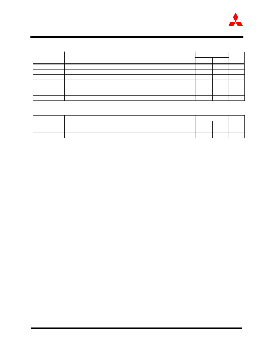
1-132
Mitsubishi microcomputers
M30240 Group
SINGLE-CHIP 16-BIT CMOS MICROCOMPUTER
Preliminary Specifications REV. E
Specifications in this manual are tentative and subject to change
Timing
Table 1.51:
External interrupt INTi inputs
Table 1.50:
Serial I/O
Symbol
Parameter
Standard
Unit
Min
Max
tc(
CK
)
CLKi input cycle time
200
ns
tw(
CKH
)
CLKi input HIGH pulse width
100
ns
tw(
CKL
)
CLKi input LOW pulse width
100
ns
td(
C
-
Q
)
TxDi output delay time
80
ns
th(
C
-
Q
)
TxDi hold time
0
ns
tsu(
D
-
C
)
RxDi input setup time
30
ns
th(
C
-
D
)
RxDi input hold time
90
ns
Symbol
Parameter
Standard
Unit
Min
Max
tw(
INH
)
INT
i input HIGH pulse width
250
ns
tw(
INL
)
INT
i input LOW pulse width
250
ns

1-133
Mitsubishi microcomputers
M30240 Group
SINGLE-CHIP 16-BIT CMOS MICROCOMPUTER
Preliminary Specifications REV. E
Specifications in this manual are tentative and subject to change
Timing Diagrams- Peripheral/interrupt
4.3 Timing Diagrams- Peripheral/interrupt
Figure 1.116: Peripheral / Interrupt timing diagram
TAi
IN
input
TAi
OUT
input
During event counter mode
t
c(TA)
t
w(TAH)
t
w(TAL)
t
c(UP)
t
w(UPH)
t
w(UPL)
t
h(T
IN
�UP)
t
su(UP�T
IN
)
TAi
IN
input
(When count on falling
edge is selected)
TAi
IN
input
(When count on rising
edge is selected)
TAi
OUT
input
(Up/down input)
t
su(D�C)
CLKi
TxDi
RxDi
t
c(AD)
t
w(ADL)
t
c(CK)
t
w(CKH)
t
w(CKL)
t
w(INL)
t
w(INH)
t
d(C�Q)
t
h(C�D)
t
h(C�Q)
INTi input
AD
TRG
input
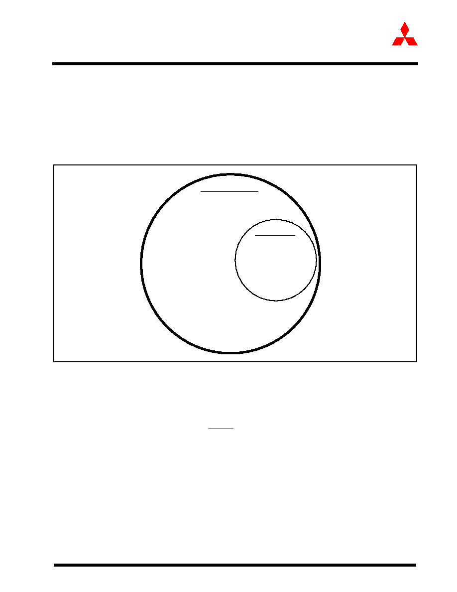
1-134
Mitsubishi microcomputers
M30240 Group
SINGLE-CHIP 16-BIT CMOS MICROCOMPUTER
Preliminary Specifications REV. E
Specifications in this manual are tentative and subject to change
Frequency Synthesizer Interface and DC-DC Converter
5.0 Applications
5.1 Frequency Synthesizer Interface and DC-DC Converter
This section presents the recommended method of setting up and using the frequency synthesizer
that generates the 48MHz clock needed by the USB FCU and the DC-DC converter that provides pow-
er to the D+/D- drivers
5.1.1 Reset of USB Related Registers
Figure 1.117: SFR Reset Venn Diagram
The special function registers (SFRs) that govern the operation of the frequency synthesizer, DC-DC
converter and USB FCU are affected by one or more reset events. The addresses of the special func-
tion registers (SFRs) that are affected by Hardware Reset, USB Reset, or both are shown in Figure
1.117.
All resettable SFRs, including SFRs and other registers internal to the USB FCU, are affected by a
Hardware Reset, which occurs when the RESET pin is brought low or an undefined opcode is fetched.
See Section 2.4 for a complete listing of SFRs and their reset values.
Only registers internal to the USB FCU are reset when a USB Reset sent by the Host/Hub is detected.
These USB registers are reset to their default values except for bit 5 of USBIS2 (USB Reset Interrupt
Status Flag), which is set to a "1". USB FCU registers are registers from address 300
16
to 33C
16
and
all other registers within the USB FCU, many of which the MCU does not have direct access to (e.g.
FIFO address pointers). The USB FIFO registers are empty after USB reset because the FIFO ad-
dress pointers are reset. However, the physical contents of the FIFOs are not set to all `1`s or all `0`s.
Other SFRs such as USBC, FSC, and CM0, CM1 are not affected by a USB Reset.
Hardware Reset
USB Reset
SFR Registers:
0004
16
to 005F
16
,
378
16
to 3FF
16
000C (USBC),
3DC
16
(FSC)
SFR Registers:
300
16
to 33C
16
(USB FCU registers)
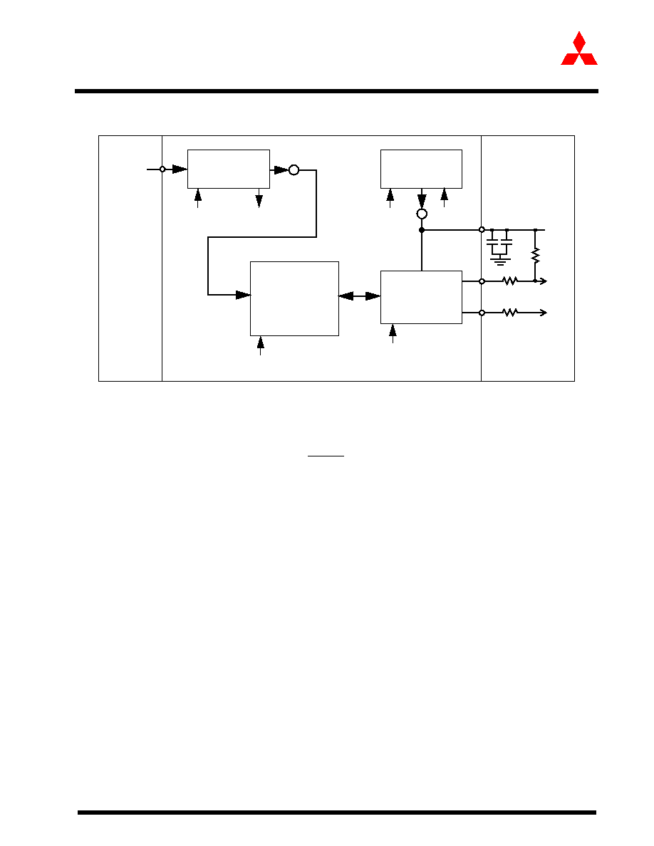
1-135
Mitsubishi microcomputers
M30240 Group
SINGLE-CHIP 16-BIT CMOS MICROCOMPUTER
Preliminary Specifications REV. E
Specifications in this manual are tentative and subject to change
Frequency Synthesizer Interface and DC-DC Converter
5.1.2 Set up of Frequency Synthesizer and DC-DC Converter
Figure 1.118: PLL, DC-DC Converter and USB Functional Block Diagram
A functional block diagram of the USB system on the M30240 which shows how the control signals
affect operation is given in Figure 1.118
5.1.2.1 Set up after Hardware Reset
A Hardware Reset occurs when either the RESET pin is brought low for more than 2
�
s or an invalid
opcode is fetched by the CPU. The frequency synthesizer (PLL) and DC-DC converter should be set
up as follows in the Hardware Reset routine (see Figure 1.119),
� Power up the M30240 and other components on the peripheral device for less than 100 mA opera-
tion. The current limit only applies for bus powered devices.
� Configure the PLL for 48MHz f(VCO) operation.
� Enable the PLL by setting FSE (bit 0 of the Frequency Synthesizer Control Register (FSC)) to a "1",
then wait for 2 ms.
� Check the lock status bit (LS, bit 7 of FSC).
�
If the bit is a "1", go on.
�
If the bit is a "0", wait 0.1 ms longer and then re-check the bit.
� Enable the DC-DC converter in high current mode by setting USBC4 (bit 4 of the USB Control Reg-
ister (USBC)) to a "1" and keeping USBC3 (bit 3 of USBC) a "0". High current mode should always
be used during normal USB operation. Low current mode should only be used during a USB sus-
pend.
� Wait (C + 1)ms (where C equals the external capacitance connected to the Ext Cap pin in
�
F) for
the voltage on Ext Cap to reach a steady state voltage of approximately 3.3V. (Since the D+ pullup
is connected to the Ext Cap pin, the upstream hub will detect that the peripheral device has been
plugged in once the voltage on D+ reaches approximately 2.0 V.)
�
Example: A 2.2
�
F
capacitor connected to Ext Cap requires 3.2 ms for the voltage on Ext Cap to be stable.
33
33
D+
D-
USB FCU
2.2
�
F
0.1
�
F
Ext Cap
Frequency
Synthesizer
f(Xin)
FSE
LS
1.5k
USB Transceiver
DC-DC Converter
USBC3
USBC4
USBC7
USBC7
USBC5
USBCLK
(48MHz)
enable
lock
enable
enable
(enable)
(enable)
enable
current
mode

1-136
Mitsubishi microcomputers
M30240 Group
SINGLE-CHIP 16-BIT CMOS MICROCOMPUTER
Preliminary Specifications REV. E
Specifications in this manual are tentative and subject to change
Frequency Synthesizer Interface and DC-DC Converter
� Enable the USB clock by setting USBC5 (bit 5 of USBC) to a "1". (If the USB clock and FCU are
enabled before the voltage on Ext Cap is stable, a phantom USB Reset may be detected, or the ac-
tual USB Reset may not be detected.)
� Wait at least 4 cycles of
, then enable the USB FCU by setting USBC7 (bit 7 of USBC) to a "1".
� Enable other blocks as necessary.
Figure 1.119: PLL and DC-DC Converter Set Up Timing after Hardware Reset
5.1.2.1.1 Precautions after Software Reset
A software reset occurs after writing a `1' to bit `3' of the processor mode register 0 (address 0004
16
). During
software reset, the contents of the internal RAM are preserved as well as all USB, DC-DC converter, and PLL
registers. If the PLL is used as the system clock source, it is important to note that after a software reset oc-
curs, any writes to the frequency synthesizer register will cause it to freeze. This can cause erratic device be-
havior. In order to avoid this, it is recommended that the following procedure be used:
�
Prior to software reset, switch device clock source from `fsyn to f(Xin)'. Please see the Frequency Synthe-
sizer specification for more details.
�
After software reset using firmware, evaluate the condition of the synthesizer control register (FSC register,
address 03DC
16
, bit `0'). This bit is not effected by a software reset and can check to see if the PLL is still
enabled. If so, any setup routine that involves writing to the PLL registers should not be called. At this point,
the clock source can be changed back to fsyn.
5.1.2.2 Set up after USB Reset Signaling Detected
A USB Reset is detected by the USB FCU when an SE0 is present on D+/D- for at least 2.5
�
s. De-
tection of a USB Reset results in bit 5 of USB Interrupt Status Register 2 (USBIS2) being set to a "1"
and the registers within the USB FCU being reset to their default values. Register USBC and the PLL
registers are not affected by a USB Reset. A USB Function Interrupt request is also generated when
the USB Reset is detected.
No modifications to the frequency synthesizer or DC-DC converter configuration should be made in
the USB Function Interrupt routine. However, all USB FCU registers (addresses 300
16
to 33C
16
) must
be reconfigured to their pre-enumeration state.
RESET
FSE
LS
USBC4
USBC5
USBC7
Wait 2
m
s
Wait (C+1)
m
s
Enable PLL
Enable DC-DC converter
Enable USB Clock
Enable USB FCU
Wait at least 4 cycles of

1-137
Mitsubishi microcomputers
M30240 Group
SINGLE-CHIP 16-BIT CMOS MICROCOMPUTER
Preliminary Specifications REV. E
Specifications in this manual are tentative and subject to change
Frequency Synthesizer Interface and DC-DC Converter
5.1.2.3 Set up after USB Suspend Detected
A USB Suspend occurs if the USB FCU does not detect any bus activity on D+/D- for at least 3 ms.
Detection of a suspend results in bit 7 of USBIS2 and bit 0 of USBPM (SUSPEND) being set to a "1".
This causes bit 3 of SUSPIC to be set to a "1". Bit 7 of USBIS2 then needs to be cleared by writing a
"1" to the bit in order to allow a future suspend event.
The configuration of the frequency synthesizer and DC-DC converter should be changed as follows in
the USB Suspend Interrupt routine (if the device is bus powered):
� Change the DC-DC converter from high current mode to low current mode by setting USBC3 (bit 3
of the USBC) to a "1"
� Disable the USB clock by setting USBC5 (bit 5 of USBC) to a "0". Once the USB clock is disabled,
registers internal to the USB FCU should not be written to. This includes all USB SFRs from address
0300
16
to 033C
16
. It does not include USBC or FSC.
� Perform other tasks to reduce total current to below 500
�
A.
� Disable the PLL by setting FSE (bit 0 of FSC) to a "0".
� Make sure the I-FLAG is set to "1".
� Stop the system clock by setting CM10 (bit 0 of CM1) to a "1". Make sure to first enable writing to the
system clock control register by setting PRCO (bit 0 of PRCR) to "1'. Also, make sure to enable the
USB Resume Interrupt (RSMIC register) and clear or execute any pending interrupts prior to stop-
ping the clock so the MCU can wake up once resume signaling is detected. If the clock is stopped
using an interrupt routine, make sure to set the priority of the Resume Interrupt (RSMIC) higher than
the current interrupt.
� Note that no action may be necessary if the device is self powered.
5.1.2.4 Set up after USB Resume Signaling Detected
A resume occurs when the USB FCU is in the suspend state and detects a non-idle signaling on D+/
D-. Detection of a resume results in bit 6 of USBIS2 and bit 1 of USBPM (RESUME) being set to a "1".
This causes bit 3 of RSMIC to also be set to "1". If the MCU was in the stop state prior to the detection
of the resume, the USB Resume Interrupt request will cause the MCU to wake up from the stop state.
Bit 6 of USBIS2 needs to be cleared (by writing a "1" to the bit) in order to allow a future resume event.
See section 2.9 "Stop Mode" for details on waking up from the stop state.
The configuration of the frequency synthesizer and DC-DC converter should be changed as follows in
the USB Resume Interrupt routine (if the device is bus powered):
� Re-enable the PLL for 48MHz f(VCO) by setting FSE (bit 0 of the FSC) to a "1", then wait for 2 ms.
� Wait for 2 ms.
� Check the lock status bit (LS, bit 7 of FSC).
�
If the bit is a "1", continue.
�
If the bit is a "0", wait 0.1
ms
longer and then re-check the bit.
� Enable the USB clock by setting USBC5 (bit 5 of USBC) to a "1".
� Wait for a minimum of 4 cycles.
� Change the DC-DC converter from low current mode to high current mode by setting USBC3 (bit 3
of the USBC) to a "0".
� Enable other blocks as necessary.
Registers internal to the USB FCU should not be written to until the USB clock is re-enabled. This in-
cludes all USB SFRs from address 0300
16
to 033C
16
. It does not include USBC or FSC.
Note that the configuration changes described above may not need to be made if the MCU was not
placed in a suspend state as described in section 5.1.2.3 Set up after USB Suspend Detected.
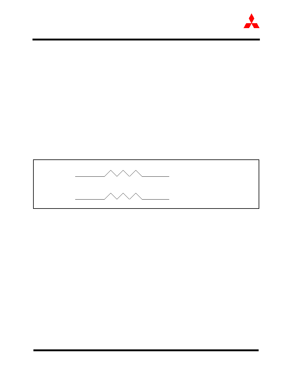
1-138
Mitsubishi microcomputers
M30240 Group
SINGLE-CHIP 16-BIT CMOS MICROCOMPUTER
Preliminary Specifications REV. E
Specifications in this manual are tentative and subject to change
Attach/Detach Function
5.1.2.5 PLL Lock Bit
The PLL lock bit is used to indicate when the PLL is first locked. Accordingly, after the PLL is enabled
and it has been given 2.0 ms to stabilize, the lock bit status should be checked. Once the lock bit is
HIGH, the USB check should be enabled. After this stage, the lock bit is no longer valid and should
not be monitored, unless the PLL is re-enabled.
5.2 Attach/Detach Function
The Attach/Detach Function can be used to attach or detach a USB function from the host without dis-
connecting the cable. When attaching a USB function, the connect registers should be set to 3 Hex at
the same time on or before the DC-DC Converter is enabled. Similarly, when detaching the connect
register, it should be set to 1 Hex when powering down the DC-DC Converter.
If you do not set the connect (address 1fh) to HIGH, the system will default to its normal mode.
Note: If the D+ is connected to ExtCAP, this mode will not work.
D+ is connected to ExtCAP through a 1.5 K resistor in compliance with the USB specification. USB
Suspend/Resume Function
Hardware connections are shown below
Attach is connected to D+ through 1.5 K resistor.
Attach [P8
3
]
D+ (pin 9 M30240)
Attach/Detach mode disabled
ExtCAP
D+ (pin 9 M30240)
1.5 K
1.5 K

1-139
Mitsubishi microcomputers
M30240 Group
SINGLE-CHIP 16-BIT CMOS MICROCOMPUTER
Preliminary Specifications REV. E
Specifications in this manual are tentative and subject to change
Low Pass Filter Network
5.3 Low Pass Filter Network
All passive components should be in close proximity to pin 78 (LPF), capacitors should be X7R di-
electric or better. The recommended values are listed in Table 1.52 . See Figure 1.120 for schematic
of the LPF.
Figure 1.120: LPF Filter Schematic
Analog V
ss
and Analog V
cc
, pins 77 and 80 should have isolated connections to the digital V
ss
and V
cc
ground planes. Figure 1.121 illustrates the power supply isolation.
Figure 1.121: Power Supply
Table 1.52:
Recommended Values
R 1000
10%
C2 = 680 pf
10%
C1 = 0.1
�
f
10%
R
C1
C2
Pin 78
(LPF)
Pin 77
A
vss
Digital
V
cc
(on card)
Digital
V
ss
Analog
V
ss
(Pin 77)
Analog
V
cc
(Pin 80)
C
C
Decoupling
Capacitors
Ferrite Beads

1-140
Mitsubishi microcomputers
M30240 Group
SINGLE-CHIP 16-BIT CMOS MICROCOMPUTER
Preliminary Specifications REV. E
Specifications in this manual are tentative and subject to change
USB Transceiver
5.4 USB Transceiver
When using the on-chip voltage converter to supply the necessary 3.3V to the driver circuit, a capac-
itor network must be connected between Ext. Cap (pin 6) and V
SS
(pin 13). Two capacitors are re-
quired as shown in Figure 1.122. The high frequency 0.1
�
F capacitor should be an X7R type or better.
The low frequency decoupling capacitor of 2.2
�
F should be of tantalum di-electric or better. The start-
up time for this value of the capacitor is 3.2 ms, approximately (1ms/
�
F) + 1 ms.
After enabling the on-chip voltage converter, a certain amount of time must pass before a wait or stop
clock instruction is executed. The amount of time is given by (C+1) ms, when C is the value in
�
F of
the external capacitance connected to the Ext. Cap pin. For example, if the external capacitance is
2.2
�
F, at least 3.2 ms must elapse from the time that the on-chip voltage converter is enabled until a
WAIT instruction or STOP command (CM10 = 1) is executed.
In order to meet the impedance matching requirements of the USB Specification, a 33
resistor must
be added to USB D+ (pin 9) and to USB D- (pin 10). In addition, capacitors connected between USB
D+ and USB D- or USB D+/D- and Vss may need to be added for rise/fall time matching and edge
control. These capacitors should be placed after the 33
resistors. Their configuration and values
will depend on the PCs layout. The placement of external components is illustrated in Figure 1.122.
Figure 1.122: Configuration of External USB components
33
33
+
_
D+
D-
XCV_Vm_in
XCV_Vp_in
XCV_Rxd
XCV_Vp_out
XCV_Suspend
XCV_Vm_out
XCV_Txen_n
Transceiver
USB_Vp_out
USB_Txen_n
USB_Vm_out
USB_Suspend
USB_Rxd
USB_Vp_in
USB_Vm_in
USB Block
Voltage Converter
2.2
�
F
0.1
�
F 10%
Ext Cap
22 pF
=
=
22 pF
10%
33 pF
(Note)
Note: Capacitor values and configuration may depend on PCB layout.
`
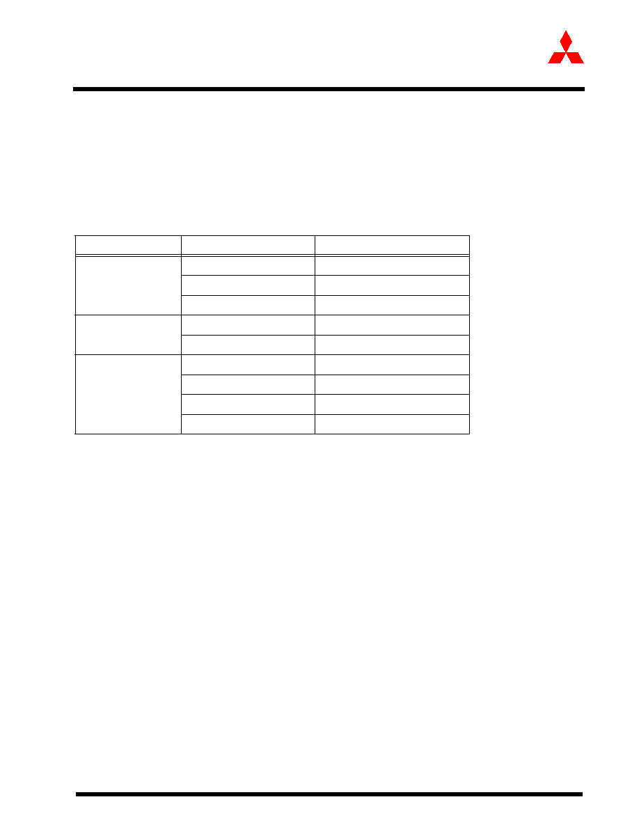
1-141
Mitsubishi microcomputers
M30240 Group
SINGLE-CHIP 16-BIT CMOS MICROCOMPUTER
Preliminary Specifications REV. E
Specifications in this manual are tentative and subject to change
Programming Notes
5.5 Programming Notes
5.5.1 Accessing USB IN/OUT CSR Registers
Do not use read-modify-write instruction on these registers because they contain control and status
bits that can be changed by both hardware and software. There is a possibility that using a read-mod-
ify-write instruction might cause incorrect data to be written back to these registers. See Table 1.53
for a list of bits that may have incorrect data written to them and the value you should write back in
order to prevent this from occurring.
The endpoint 1-4 IN CSR's (EPiICS, i = 1-4) have a bit IN_PKT_RDY (bit 0) that is set to a "1" by the
firmware after a packet of data is loaded to the respective endpoint's FIFO. This signifies that a packet
is ready for transmission. If the firmware wants to send a NULL packet to the host, it can simply write
a "1" to the IN_PKT_RDY bit without loading data to the FIFO. This bit is cleared by the hardware. If
the firmware manipulates (writes) the IN CSR for a purpose other than to signify to the hardware that
a data packet is ready for transmission (for instance, set/reset ISO bit, set/reset SEND_STALL bit), it
must make sure that a "0" is written back to the IN_PKT_RDY bit. Failure to do so could cause improp-
er operation of the device. Writing a "0" to the IN_PKT_RDY bit has no effect on its state.
The endpoint 1-4 OUT CSRs (EPiICS, i = 1-4) have a bit OUT_PKT_RDY (bit 0) that is set to a "1" by
the hardware after a packet of data is received from the host to the respective endpoint's FIFO. This
signifies that a packet is ready for download. This bit is cleared by the firmware by writing a "0" to it
after the data packet is unloaded from the FIFO. If the firmware manipulates (writes) the OUT CSR for
a purpose other than to signify to the hardware that a data packet has been unloaded (for instance,
set/reset ISO bit, set/reset SEND_STALL bit), it must make sure that a "1" is written back to the
OUT_PKT_RDY bit. Failure to do so could cause improper operation. Writing a "1" to the
OUT_PKT_RDY bit has no effect on its state.
Table 1.53:
Bits that might have incorrect data
Register name
Bit name
Value to write for "No change"
EP0CS
IN_PKT_RDY (b1)
"0"
DATA_END (b3)
"0"
FORCE_STALL (b4)
"1"
EPxICS (x = 1-4)
IN_PKT_RDY (b0)
"0"
UNDER_RUN (b1)
"1"
EPxOCS (x = 1-4)
OUT_PKT_RDY (b0)
"1"
OVER_RUN (b1)
"1"
FORCE_STALL (b4)
"1"
DATA-ERR (b5)
"1"

1-142
Mitsubishi microcomputers
M30240 Group
SINGLE-CHIP 16-BIT CMOS MICROCOMPUTER
Preliminary Specifications REV. E
Specifications in this manual are tentative and subject to change
Programming Notes
Below is an example of how to set/reset the ISO bit of the IN CSR register (for initializing the respective
endpoint as an isochronous endpoint):
5.5.2 USB Consecutive Set Address
The USB Specification states that the host can send a SET_ADDRESS request for the following cas-
es:
1. During enumeration when the device is in default state. (The host assigns a non-zero address.)
2. When the device is in the address state. (The host can re-assign a new address.)
The device handles case #1 (when the device is in the default state) and case #2 (when the device is
in the address state) differently. The following is a segment of code to illustrate the program flow to
properly deal with these cases.
Note: wValue_lo = assigned address from the host in SET-ADDRESS request.
[R1L] = [EPiICS].B
OR.B #08H, R1L
;set ISO bit = 1, write "1" back to UNDER_RUN bit
AND.B #0FEH, R1L
;write "0" back to IN_PKT_RDY bit
[EPiICS].B = [R1L]
[R1L] = [EPiICS].B
OR.B #02, R1L
;write "1" back to UNDER_RUN bit
AND.B #0F6H, R1L
;reset ISO bit = 0, write "0" back to IN_PKT_RDY bit
[EPiICS].B= [R1L]
DEFAULT_STATE:
If [USBA].B ==0
[USBA.].B = wValue _ lo
;If the device is in default state, update address before STATUS
completion
R1L = [EP0CS].B
;USB ENDPOINT 0 CSR
OR.B #48H, R1L
;Set serviced_out_pkt_rdy & data_end
[EP0CS].B = R1L
wait for the completion of the
JMP ADDR_END
else
ADDR_STATE
R1L [EP0CS].B
;USB ENDPOINT 0 CSR
OR.B #48H, R1L
;Set serviced_out_pkt_rdy & data_end
[EP0CS].B = R1L
wait for the completion of the
[USBA].B= wValue_lo
;If the device is in address state, update address before STATUS
completion
ADDR_END
endif
end of the set_address routine