Mitsubishi microcomputers
M16C / 61 Group
SINGLE-CHIP 16-BIT CMOS MICROCOMPUTER
Description
1
------Table of Contents------
Description
The M16C/61 group of single-chip microcomputers are built using the high-performance silicon gate
CMOS process using a M16C/60 Series CPU core and are packaged in a 100-pin plastic molded QFP.
These single-chip microcomputers operate using sophisticated instructions featuring a high level of in-
struction efficiency. With 1M bytes of address space, they are capable of executing instructions at high
speed. They also feature a built-in multiplier and DMAC, making them ideal for controlling office, communi-
cations, industrial equipment, and other high-speed processing applications.
The M16C/61 group includes a wide range of products with different internal memory types and sizes and
various package types.
Features
· Memory capacity ............................................ ROM (See Figure 1.1.4. ROM Expansion)
RAM 4K to 10K bytes
· Shortest instruction execution time ................ 100ns (f(X
IN
)=10MH
Z
)
· Supply voltage ............................................... 4.0 to 5.5V (f(X
IN
)=10MH
Z
)
2.7 to 5.5V (f(X
IN
)=7MH
Z
with software one-wait)
· Low power consumption ................................ 18mW ( f(X
IN
)=7MH
Z
, with software one-wait, V
CC
= 3V)
· Interrupts ........................................................ 20 internal and 5 external interrupt sources, 4 software
interrupt sources; 7 levels (including key input interrupt)
· Multifunction 16-bit timer ................................ 5 output timers + 3 input timers
· Serial I/O (UART or clock synchronous) ........ 3 channels
· DMAC ............................................................ 2 channels (trigger: 16 sources)
· A-D converter ................................................. 10 bits X 8 channels
(Expandable up to 10 channels)
· D-A converter ................................................. 8 bits X 2 channels
· CRC calculation circuit ................................... 1 circuit
· Watchdog timer .............................................. 1 line
· Programmable I/O ......................................... 87 lines
· Input port ........................................................
_______
1 line (P8
5
shared with NMI pin)
· Memory expansion ........................................ Available (to a maximum of 1M bytes)
· Chip select output .......................................... 4 lines
· Clock generating circuit ................................. 2 built-in clock generation circuits
(built-in feedback resistor, and external ceramic or quartz oscillator)
Applications
Audio, cameras, office equipment, communications equipment, portable equipment
Timer ............................................................. 70
Serial I/O ....................................................... 87
A-D Converter ............................................. 114
D-A Converter ............................................. 124
CRC Calculation Circuit .............................. 126
Programmable I/O Ports ............................. 128
Electrical Characteristics ............................. 142
Central Processing Unit (CPU) ..................... 11
Reset ............................................................. 14
Processor Mode ............................................ 19
Clock Generating Circuit ............................... 30
Protection ...................................................... 39
Interrupts ....................................................... 40
Watchdog Timer ............................................ 59
DMAC ........................................................... 61
Mitsubishi microcomputers
M16C / 61 Group
SINGLE-CHIP 16-BIT CMOS MICROCOMPUTER
Description
4
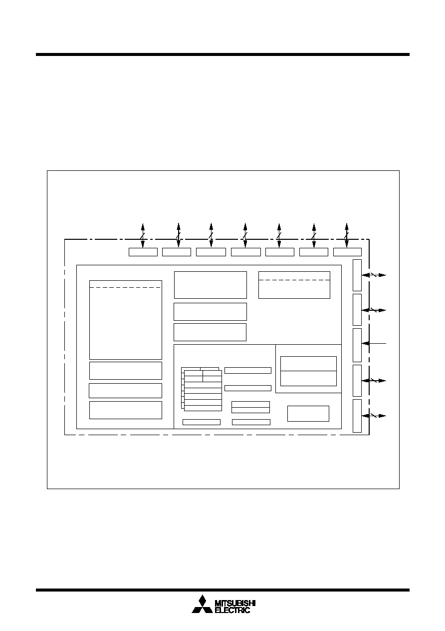
Block Diagram
Figure 1.1.3 is a block diagram of the M16C/61 group.
Block diagram of the M16C/61 group
Timer
Timer TA0 (16 bits)
Timer TA1 (16 bits)
Timer TA2 (16 bits)
Timer TA3 (16 bits)
Timer TA4 (16 bits)
Timer TB0 (16 bits)
Timer TB1 (16 bits)
Timer TB2 (16 bits)
Internal peripheral functions
Watchdog timer
(15 bits)
DMAC
(2 channels)
D-A converter
(8 bits X 2 channels)
A-D converter
(10 bits
X
8 channels
Expandable up to 10 channels)
UART/clock synchronous SI/O
(8 bits
X
3channels) (Note 3)
System clock generator
X
IN
-X
OUT
X
CIN
-X
COUT
M16C/60 series16-bit CPU core
I/O ports
Port P0
8
Port P1
8
Port P2
8
Port P3
8
Port P4
8
Port P5
8
Port P6
8
8
R0L
R0H
R1H
R1L
R2
R3
A0
A1
FB
R0L
R0H
R1H
R1L
R2
R3
A0
A1
FB
Registers
ISP
USP
Stack pointer
Vector table
INTB
CRC arithmetic circuit (CCITT )
(Polynomial : X
16
+X
12
+X
5
+1)
Multiplier
7
8
8
Port P10
Port P9
Port P8
Port P7
Memory
Port P8
5
ROM
(Note 1)
RAM
(Note 2)
Note 1: ROM size depends on MCU type.
Note 2: RAM size depends on MCU type.
Note 3: One of serial I/O can use for SIM interface.
SB
FLG
PC
Program counter
Figure 1.1.3. Block diagram of M16C/61 group
Mitsubishi microcomputers
M16C / 61 Group
SINGLE-CHIP 16-BIT CMOS MICROCOMPUTER
Description
5
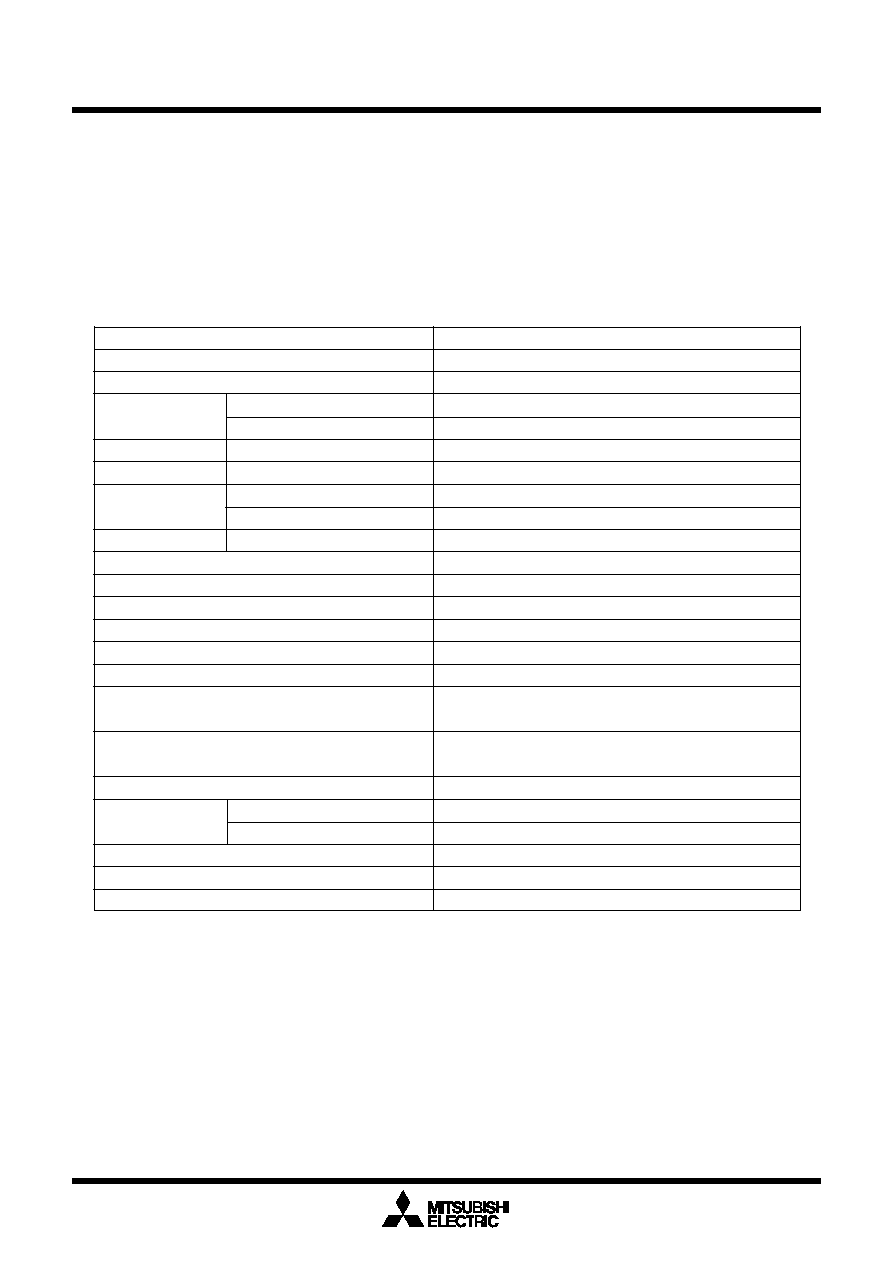
Item
Performance
Number of basic instructions
91 instructions
Shortest instruction execution time
100ns(f(X
IN
)=10MH
Z
)
Memory
ROM
(See the Figure 4. ROM Expansion)
capacity
RAM
4K to 10K bytes
I/O port
P0 to P10 (except P8
5
)
8 bits x 10, 7 bits x 1
Input port
P8
5
1 bit x 1
Multifunction
TA0, TA1, TA2, TA3, TA4
16 bits x 5
timer
TB0, TB1, TB2
16 bits x 3
Serial I/O
UART0, UART1, UART2
(UART or clock synchronous) x 3
A-D converter
10 bits x (8 + 2) channels
D-A converter
8 bits x 2
DMAC
2 channels (trigger: 16 sources)
CRC calculation circuit
CRC - CCITT
Watchdog timer
15 bits x 1 (with prescaler)
Interrupt
20 internal and 5 external sources, 4 software sources, 7 levels
Clock generating circuit
2 built-in clock generation circuits
(built-in feedback resistor, and external ceramic or quartz oscillator)
Supply voltage
4.0 to 5.5V (f(X
IN
) = 10MH
Z
)
2.7 to 5.5V(f(X
IN
)=7MH
Z
with software one-wait)
Power consumption
18mW (f(X
IN
) = 7MH
Z
with software one-wait,V
CC
= 3V)
I/O
I/O withstand voltage
5V
characteristics
Output current
5mA
Memory expansion
Available (to a maximum of 1M bytes)
Device configuration
CMOS silicon gate
Package
100-pin plastic mold QFP
Table 1.1.1. Performance outline of M16C/61 group
Performance Outline
Table 1.1.1 is a performance outline of M16C/61 group.