01-Description DATASHEET SEARCH SITE | WWW.ALLDATASHEET.COM

1
Mitsubishi microcomputers
M16C / 62T Group
SINGLE-CHIP 16-BIT CMOS MICROCOMPUTER
Description
------Table of Contents------
Description
The M16C/62T group of single-chip microcomputers are built using the high-performance silicon gate
CMOS process using a M16C/60 Series CPU core and are packaged in a 100-pin or a 80-pin plastic
molded QFP. These single-chip microcomputers operate using sophisticated instructions featuring a high
level of instruction efficiency. With 1M bytes of address space, they are capable of executing instructions at
high speed. They also feature a built-in multiplier and DMAC, making them ideal for controlling office,
communications, industrial equipment, and other high-speed processing applications.
The M16C/62T group includes a wide range of products with different internal memory types and sizes and
various package types.
Features
· Memory capacity .................................. M30623M4T-XXXGP : ROM 32K bytes, RAM 3K bytes
M30622M8T/M8V-XXXFP,M30623M8T/M8V-XXXGP : ROM 64K bytes, RAM 4K bytes
M30622MCT/MCV-XXXFP,M30623MCT/MCV-XXXGP : ROM 128K bytes, RAM 5K bytes
M30622ECT/ECV-XXXFP,M30623ECT/ECV-XXXGP : PROM 128K bytes, RAM 5K bytes
· Shortest instruction execution time ......62.5ns (f(X
IN
)=16MH
Z
, V
CC
=5V)
· Supply voltage ..................................... Mask ROM version : 4.2 to 5.5V (f(X
IN
)=16MH
Z
, without software wait)
One-time PROM version : 4.5 to 5.5V (f(X
IN
)=16MH
Z
, without software wait)
· Low power consumption ......................140mW (V
CC
= 5V, f(X
IN
)=16MH
Z
)
· Interrupts
25 internal interrupt sources, 8 external interrupt sources (M30622(100-pin package))
/5 sources (M30623(80-pin package)), 4 software interrupt sources,
7 levels (including key input interrupt)
· Multifunction 16-bit timer ......................5 I/O timers + 6 input timers(M30622(100-pin package))
3 I/O timers + 5 input timers(M30623(80-pin package))
· Inside 16-bit timer ................................ 3 timers(only M30623(80-pin package))(Note 1)
· Serial I/O .............................................. · M30622(100-pin package) : 3 for UART or clock synchronous + 2 for synchronous
· M30623(80-pin package) : 3 for UART or clock synchronous(one of exclusive UART)
+ 2 for synchronous(one of exclusive transmission)
· DMAC .................................................. 2 channels (trigger: 24 sources)
· A-D converter ....................................... 10 bits X 8 channels (Expandable up to 26 channels)
· D-A converter ....................................... 8 bits X 2 channels
· CRC calculation circuit ......................... 1 circuit
· Watchdog timer .................................... 1 line
· Programmable I/O ...............................87 lines(M30622(100-pin package)),70 lines(M30623(80-pin package))
· Input port ..............................................
_______
1 line (P8
5
shared with NMI pin)
· Memory expansion .............................. Available (to 1.2M bytes or 4M bytes)
· Chip select output ................................ 4 lines(only M30622(100-pin package))(Note 2)
· Clock generating circuit ....................... 2 built-in clock generation circuits (built-in feedback resistor, and external ceramic or quartz oscillator)
Note 1: In M30623(80-pin package), these timers have no corresponding external pin can be used as
internal timers.
Note 2: M30623(80-pin package) has no external pin for chip select output.
Applications
Audio, cameras, office equipment, communications
equipment, portable equipment, cars, etc
Central Processing Unit (CPU) ..................... 12
Reset ............................................................. 15
Processor Mode ............................................ 28
Clock Generating Circuit ............................... 40
Protection ...................................................... 49
Interrupts ....................................................... 50
Watchdog Timer ............................................ 70
DMAC ........................................................... 72
Specifications written in this manual are believed to be accurate, but are
not guaranteed to be entirely free of error.
Specifications in this manual may be changed for functional or performance
improvements. Please make sure your manual is the latest edition.
Timer ............................................................. 82
Timers' function for three-phase motor control.......... 100
Serial I/O ..................................................... 112
A-D Converter ............................................. 146
D-A Converter ............................................. 157
CRC Calculation Circuit .............................. 159
Programmable I/O Ports ............................. 161
Electrical characteristics ............................. 176
Mitsubishi microcomputers
M16C / 62T Group
SINGLE-CHIP 16-BIT CMOS MICROCOMPUTER
2
Description
80
79
P1
0
/D
8
P1
1
/D
9
78
77
P1
2
/D
10
P1
3
/D
11
76
75
P1
4
/D
12
P1
5
/D
13
/INT
3
74
73
P1
6
/D
14
/INT
4
P1
7
/D
15
/INT
5
72
71
P2
0
/AN
20
/A
0
(/D
0
/-)
P2
1
/AN
21
/A
1
(/D
1
/D
0
)
70
69
P2
2
/AN
22
/A
2
(/D
2
/D
1
)
P2
3
/AN
23
/A
3
(/D
3
/D
2
)
68
67
P2
4
/AN
24
/A
4
(/D
4
/D
3
)
P2
5
/AN
25
/A
5
(/D
5
/D
4
)
66
65
P2
6
/AN
26
/A
6
(/D
6
/D
5
)
P2
7
/AN
27
/A
7
(/D
7
/D
6
)
64
63
V
SS
P3
0
/A
8
(/-/D
7
)
62
61
V
CC
P3
1
/A
9
60
59
P3
2
/A
10
P3
3
/A
11
58
57
P3
4
/A
12
P3
5
/A
13
56
55
P3
6
/A
14
P3
7
/A
15
54
53
P4
0
/A
16
P4
1
/A
17
52
51
P4
2
/A
18
P4
3
/A
19
50
P4
4
/CS0
49
P4
5
/CS1
48
P4
6
/CS2
47
P4
7
/CS3
46
P5
0
/WRL/WR
45
P5
1
/WRH/BHE
44
P5
2
/RD
43
P5
3
/BCLK
42
P5
4
/HLDA
41
P5
5
/HOLD
40
P5
6
/ALE
39
P5
7
/RDY/CLK
OUT
38
P6
0
/CTS
0
/RTS
0
37
P6
1
/CLK
0
36
P6
2
/RxD
0
35
P6
3
/TxD
0
34
P6
4
/CTS
1
/RTS
1
/CTS
0
/CLKS
1
33
P6
5
/CLK
1
32
P6
6
/RxD
1
31
P6
7
/TxD
1
1
2
3
4
5
6
7
8
9
10
11
12
13
14
15
16
17
18
19
20
21
22
23
24
25
26
27
28
29
30
P9
5
/ANEX0/CLK
4
P9
4
/DA
1
/TB4
IN
P9
3
/DA
0
/TB3
IN
P9
2
/TB2
IN
/S
OUT3
P9
1
/TB1
IN
/S
IN3
P9
0
/TB0
IN
/CLK
3
BYTE
CNV
SS
P8
7
/X
CIN
P8
6
/X
COUT
RESET
X
OUT
V
SS
X
IN
V
CC
P8
5
/NMI
P8
4
/INT
2
P8
3
/INT
1
P8
2
/INT
0
P8
1
/TA4
IN
/U
P8
0
/TA4
OUT
/U
P7
7
/TA3
IN
P7
6
/TA3
OUT
P7
5
/TA2
IN
/W
P7
4
/TA2
OUT
/W
P7
3
/CTS
2
/RTS
2
/TA1
IN
/V
P7
2
/CLK
2
/TA1
OUT
/V
P7
1
/RxD
2
/SCL/TA0
IN
/TB5
IN
P7
0
/TxD
2
/SDA/TA0
OUT
81
82
83
84
85
86
87
88
89
90
91
92
93
94
95
96
97
98
99
100
P0
7
/AN
07
/D
7
P0
6
/AN
06
/D
6
P0
5
/AN
05
/D
5
P0
4
/AN
04
/D
4
P0
3
/AN
03
/D
3
P0
2
/AN
02
/D
2
P0
1
/AN
01
/D
1
P0
0
/AN
00
/D
0
P10
7
/AN
7
/KI
3
P10
6
/AN
6
/KI
2
P10
5
/AN
5
/KI
1
P10
4
/AN
4
/KI
0
P10
3
/AN
3
P10
2
/AN
2
P10
1
/AN
1
AV
SS
P10
0
/AN
0
V
REF
P9
7
/AD
TRG
/S
IN4
P9
6
/ANEX1/S
OUT4
AV
CC
M16C/62T Group
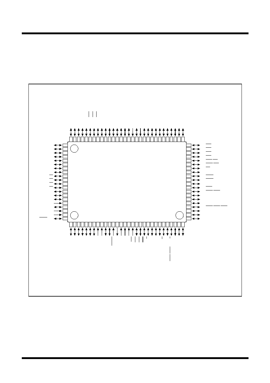
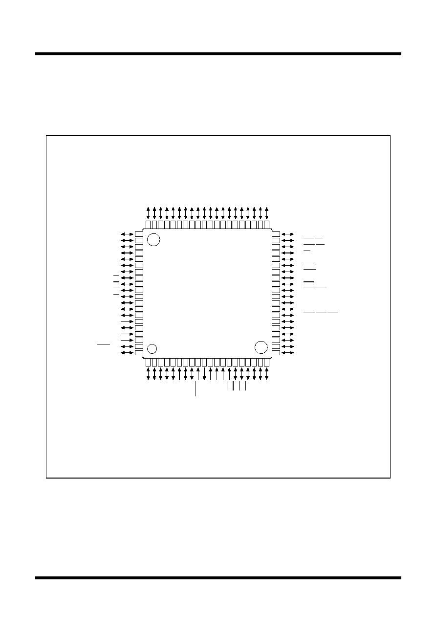
Pin Configuration
Figures 1.1.1 show the pin configurations (top view) of M30622(100-pin package) and 1.1.2 show the pin
configurations (top view) of M30623(80-pin package).
PIN CONFIGURATION (top view)
Figure 1.1.1. Pin configuration (top view) of M30622 (100-pin package)
Package: 100P6S-A
3
Mitsubishi microcomputers
M16C / 62T Group
SINGLE-CHIP 16-BIT CMOS MICROCOMPUTER
Description
60
59
58
57
56
55
54
53
52
51
P2
0
/AN
20
/A
0
(/D
0
)
P2
1
/AN
21
/A
1
(/D
1
)
50
49
P2
2
/AN
22
/A
2
(/D
2
)
P2
3
/AN
23
/A
3
(/D
3
)
48
47
P2
4
/AN
24
/A
4
(/D
4
)
P2
5
/AN
25
/A
5
(/D
5
)
46
45
P2
6
/AN
26
/A
6
(/D
6
)
P2
7
/AN
27
/A
7
(/D
7
)
44
43
P3
0
/A
8
42
41
P3
1
/A
9
P3
2
/A
10
P3
3
/A
11
P3
4
/A
12
P3
5
/A
13
P3
6
/A
14
P3
7
/A
15
P4
0
/A
16
P4
1
/A
17
P4
2
/A
18
40
39
38
37
36
P5
0
/WRL/WR
35
P5
1
/WRH/BHE
34
P5
2
/RD
33
P5
3
/BCLK
32
P5
4
/HLDA
31
P5
5
/HOLD
30
P5
6
/ALE
29
P5
7
/RDY/CLK
OUT
28
P6
0
/CTS
0
/RTS
0
27
P6
1
/CLK
0
26
P6
2
/RxD
0
25
P6
3
/TxD
0
24
P6
4
/CTS
1
/RTS
1
/CTS
0
/CLKS
1
23
P6
5
/CLK
1
22
P6
6
/RxD
1
21
P6
7
/TxD
1
1
2
3
4
5
6
7
8
9
10
11
12
13
14
15
16
17
18
19
20
P9
5
/ANEX0/CLK
4
P9
4
/DA
1
/TB4
IN
P9
3
/DA
0
/TB3
IN
P9
2
/TB2
IN
/S
OUT3
P9
0
/TB0
IN
/CLK
3
CNV
SS
(BYTE)
P8
7
/X
CIN
P8
6
/X
COUT
RESET
X
OUT
V
SS
X
IN
V
CC
P8
5
/NMI
P8
4
/INT
2
P8
3
/INT
1
P8
2
/INT
0
P8
1
/TA4
IN
P8
0
/TA4
OUT
P7
7
/TA3
IN
61
62
63
64
65
66
67
68
69
70
71
72
73
74
75
76
77
78
79
80
P0
6
/AN
06
/D
6
P0
5
/AN
05
/D
5
P0
4
/AN
04
/D
4
P0
3
/AN
03
/D
3
P0
2
/AN
02
/D
2
P0
1
/AN
01
/D
1
P0
0
/AN
00
/D
0
P10
7
/AN
7
/KI
3
P10
6
/AN
6
/KI
2
P10
5
/AN
5
/KI
1
P10
4
/AN
4
/KI
0
P10
3
/AN
3
P10
2
/AN
2
P10
1
/AN
1
AV
SS
P10
0
/AN
0
V
REF
P9
7
/AD
TRG
/S
IN4
AV
CC
M16C/62T Group
P9
6
/ANEX1/S
OUT4
P7
0
/TxD
2
/SDA/TA0
OUT
P7
1
/RxD
2
/SCL/TA0
IN
/TB5
IN
P7
6
/TA3
OUT
P4
3
/A
19
P0
7
/AN
07
/D
7
Figure 1.1.2. Pin configuration (top view) of M30623 (80-pin package)
Package: 80P6S-A
PIN CONFIGURATION (top view)
Mitsubishi microcomputers
M16C / 62T Group
SINGLE-CHIP 16-BIT CMOS MICROCOMPUTER
4
Description
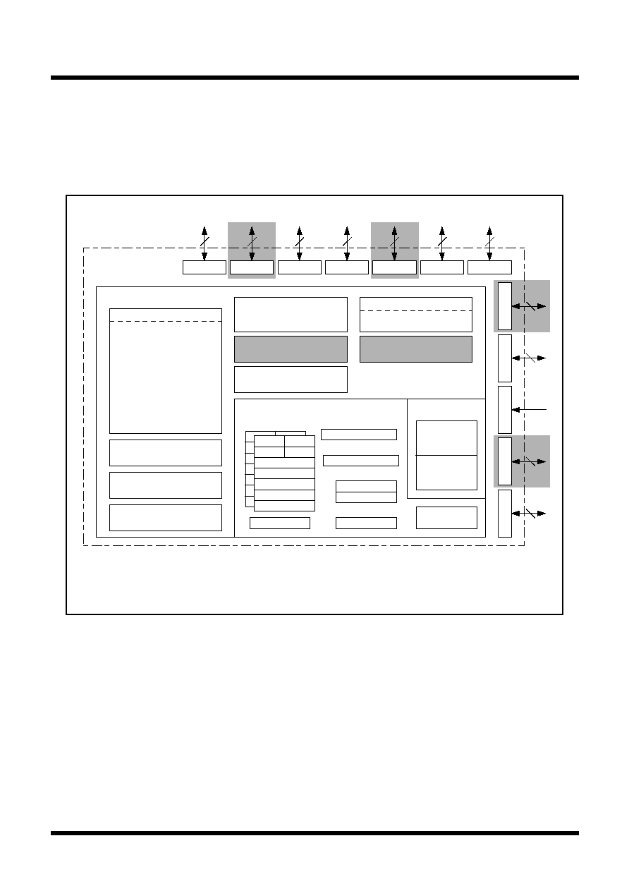
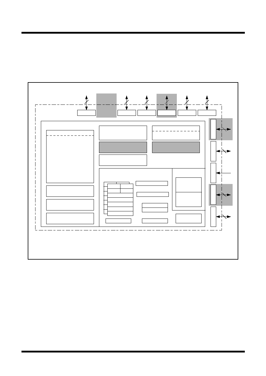
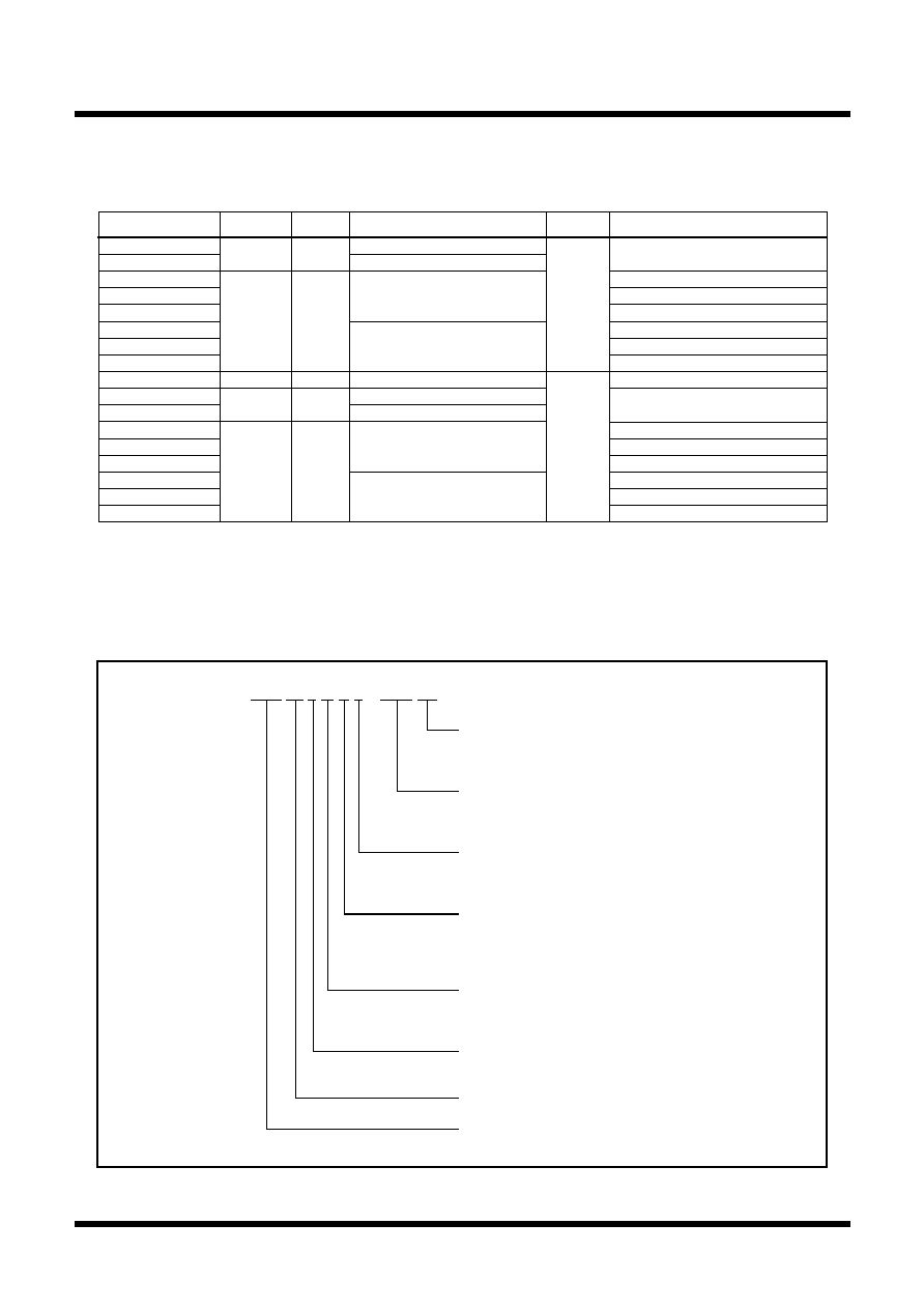
Block Diagram
Figure 1.1.3 is block diagrams of M30622(100-pin package) and 1.1.4 is block diagrams of M30623(80-pin
package).
I/O ports
Port P0
8
Port P1
8
Port P2
8
Port P3
8
Port P4
8
Port P5
8
Port P6
8
Port P7
8
Port P8
7
Port P8
5
Port P9
8
Port P10
8
Internal peripheral functions
Timer
Timer TA0 (16 bits)
Timer TA1 (16 bits)
Timer TA2 (16 bits)
Timer TA3 (16 bits)
Timer TA4 (16 bits)
Timer TB0 (16 bits)
Timer TB1 (16 bits)
Timer TB2 (16 bits)
Timer TB3 (16 bits)
Timer TB4 (16 bits)
Timer TB5 (16 bits)
Watchdog timer
(15 bits)
DMAC
(2 channels)
D-A converter
(8 bits
!
2 channels)
SB
Registers
Program conter
R0H
R0L
R1H
R1L
R2
R3
A0
A1
FB
PC
Sutack pointer
ISP
USP
Vector table
INTB
FLG
M16C/60series 16-bit CPU core
Memory
Multiplier
A-D converter
(10 bits
!
8 channels
Expandable up to 26 channels)
UART/clock synchronous SI/O
(8 bits
!
3 channels) (Note 1)
CRC arithmetic circuit (CCITT)
(Polynominal: X
16
+X
12
+X
5
+1)
System clock generator
X
IN
-X
OUT
X
CIN
-X
COUT
Clock synchronous SI/O
(8 bits
!
2 channels)
ROM
(Note 2)
RAM
(Note 3)
R0H
R0L
R1H
R1L
R2
R3
A0
A1
FB
Note 1: One of 3 channels also functions as IIC bus interface.
Note 2: ROM size depends on MCU type.
Note 3: RAM size depends on MCU type.
Figure 1.1.3. Block diagram of M30622 (100-pin package)
5
Mitsubishi microcomputers
M16C / 62T Group
SINGLE-CHIP 16-BIT CMOS MICROCOMPUTER
Description
Figure 1.1.4. Block diagram of M30623 (80-pin package)
I/O ports
Port P0
8
Port P2
8
Port P3
8
Port P4
4
Port P5
8
Port P6
8
Port P7
4
Port P8
7
Port P8
5
Port P9
7
Port P10
8
Internal peripheral functions
Timer
Timer TA0 (16 bits)
Timer TA1 (16 bits)
Timer TA2 (16 bits)
Timer TA3 (16 bits)
Timer TA4 (16 bits)
Timer TB0 (16 bits)
Timer TB1 (16 bits)
Timer TB2 (16 bits)
Timer TB3 (16 bits)
Timer TB4 (16 bits)
Timer TB5 (16 bits)
Watchdog timer
(15 bits)
DMAC
(2 channels)
D-A converter
(8 bits
!
2 channels)
SB
Registers
Program conter
R0H
R0L
R1H
R1L
R2
R3
A0
A1
FB
PC
Sutack pointer
ISP
USP
Vector table
INTB
FLG
M16C/60series 16-bit CPU core
Memory
Multiplier
A-D converter
(10 bits
!
8 channels
Expandable up to 26 channels)
UART/clock synchronous SI/O
(8 bits
!
3 channels) (Note 1)
CRC arithmetic circuit (CCITT)
(Polynominal: X
16
+X
12
+X
5
+1)
System clock generator
X
IN
-X
OUT
X
CIN
-X
COUT
Clock synchronous SI/O
(8 bits
!
2 channels) (Note 2)
ROM
(Note 3)
RAM
(Note 4)
R0H
R0L
R1H
R1L
R2
R3
A0
A1
FB
Note 1: One of 3 channels is an exclusive UART, functions as IIC bus interface.
Note 2: One of 3 channels is an exclusive transmission.
Note 3: ROM size depends on MCU type.
Note 4: RAM size depends on MCU type.
Mitsubishi microcomputers
M16C / 62T Group
SINGLE-CHIP 16-BIT CMOS MICROCOMPUTER
6
Description
Performance Outline
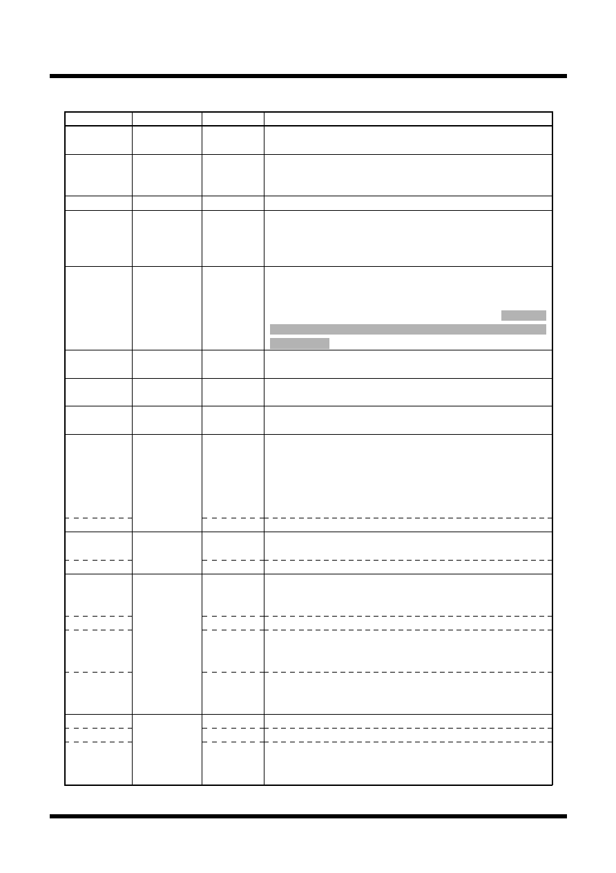
Table 1.1.1 is a performance outline of M16C/62T group.
Item
Performance
M30622(100-pin package)
M30623(80-pin package)
Number of basic instructions
91 instructions
Shortest instruction execution time
62.5ns(f(X
IN
)=16MH
Z
, V
CC
=5V)
Memory
ROM
32Kbytes (M30623M4T-XXXGP)
capacity
64Kbytes (M30622M8T/M8V-XXXFP, M30623M8T/M8V-XXXGP)
128Kbytes (M30622MCT/MCV-XXXFP, M30623MCT/MCV-XXXGP,
M30622ECT/ECV-XXXFP, M30623ECT/ECV-XXXGP)
RAM
3Kbytes (M30623M4T-XXXGP)
4Kbytes (M30622M8T/M8V-XXXFP, M30623M8T/M8V-XXXGP)
5Kbytes (M30622MCT/MCV-XXXFP, M30623MCT/MCV-XXXGP,
M30622ECT/ECV-XXXFP, M30623ECT/ECV-XXXGP)
I/O port
P0, P2, P3, P5, P6, P10
8 bits x 6
P1
8 bits x 1
-
P4, P7
8 bits x 2
4 bits x 2
P8 (except P8
5
)
7 bits x 1
P9
8 bits x 1
7 bits x 1
Input port
P8
5
1 bit x 1
Multifunction
TA0, A3, TA4
16 bits x 3 (cycle timer, external / internal event count, pulse output)
timer
TA1, TA2
16 bits x 2
16 bits x 2
(cycle timer, external / internal event count, pulse output)
(cycle timer, internal event count)
TB0, TB2 to TB5
16 bits x 5
(cycle timer, external / internal event count, pulse period / pulse width measurement)
TB1
16 bits x 1
(cycle timer, external / internal event
16 bits x 1
count, pulse period / pulse width measurement)
(cycle timer, internal event count)
Serial I/O
UART0, UART1
(UART or clock synchronous) x 2
UART2
(UART or clock synchronous) x 1
UART x 1
SI/O3
(Clock synchronous) x 1
(Clock synchronous) x 1
(exclusive transmission)
SI/O4
(Clock synchronous) x 1
A-D converter
10 bits x (8 x 3 + 2) channels
D-A converter
8 bits x 2 channels
DMAC
2 channels (trigger: 24 sources)
CRC calculation circuit
CRC-CCITT
Watchdog timer
15 bits x 1 (with prescaler)
Interrupt
25 internal and 8 external sources,
25 internal and 5 external sources,
4 software sources, 7 levels
4 software sources, 7 levels
Clock generating circuit
2 built-in clock generation circuits
(built-in feedback resistor, and external ceramic or quartz oscillator)
Supply voltage
Mask ROM version : 4.2 to 5.5V (f(X
IN
)=16MH
Z
, without software wait)
One-time PROM version : 4.5 to 5.5V (f(X
IN
)=16MH
Z
, without software wait)
Power consumption
140mW (V
CC
=5V, f(X
IN
) = 16MH
Z
)
I/O
I/O withstand voltage
5V
characteristics
Output current
5mA
Memory expansion
Available (to 1.2M bytes or 4M bytes)
(The M16C/62T group is not guaranteed to operate in memory expansion.)
Operating ambient temperature
85
°
C guaranteed version : -40
°
C to 85
°
C, 125
°
C guaranteed version : -40
°
C to 125
°
C
Device configuration
CMOS high performance silicon gate
Package
100-pin plastic mold QFP
80-pin plastic mold QFP
Table 1.1.1. Performance outline of M16C/62T group
7
Mitsubishi microcomputers
M16C / 62T Group
SINGLE-CHIP 16-BIT CMOS MICROCOMPUTER
Description
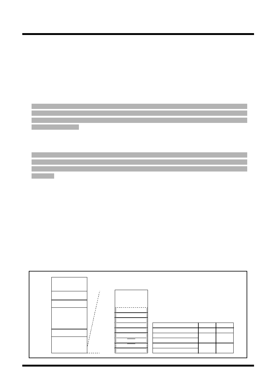
Mitsubishi plans to release the following products in the M16C/62T group:
(1) Support for mask ROM version, one-time PROM version
One-time PROM version has the equally functions mask ROM version, with the exception of built-in
electolic-programming-possible PROM.
(2) ROM capacity
(3) Package(number of pin)
100P6S-A
: 100-pin plastic molded QFP
80P6S-A
: 80-pin plastic molded QFP
(4) Support for 85
°
C guaranteed version, 125
°
C guaranteed version
125
°
C guaranteed version M30622MxV/ECV-XXXFP, M30623MxV/ECV-XXXGP is suported. These are
different from 85
°
C guaranteed version M30622MxT/ECT-XXXFP, M30623MxT/ECT-XXXGP on operating
ambient temperature and the terms of the use, and so please inquire.
100-pin packaege
64K bytes
128K bytes
Mask ROM version
One-time PROM version
ROM size
M30623M8T-XXXGP
M30623M8V-XXXGP
M30623MCT-XXXGP
M30623MCV-XXXGP
U
Shipped in blank
M30622MCT-XXXFP
M30622MCV-XXXFP
M30622M8T-XXXFP
M30622M8V-XXXFP
M30622ECT-XXXFP
M30622ECTFP
M30622ECV-XXXFP
M30622ECVFP
80-pin packaege
U
U
M30623ECT-XXXGP
M30623ECTGP
M30623ECV-XXXGP
M30623ECVGP
32K bytes
M30623M4T-XXXGP
U
U
Mask ROM version
One-time PROM version
Note 1: It may change in the future.
Note 2: Use shipped in blank of one-time PROM version as the trial, development of program.
In case of vehicle-mount test or mass production, use shipped in programming.
Figure 1.1.5. ROM expansion
Now: Mar.1999.
Mitsubishi microcomputers
M16C / 62T Group
SINGLE-CHIP 16-BIT CMOS MICROCOMPUTER
8
Description
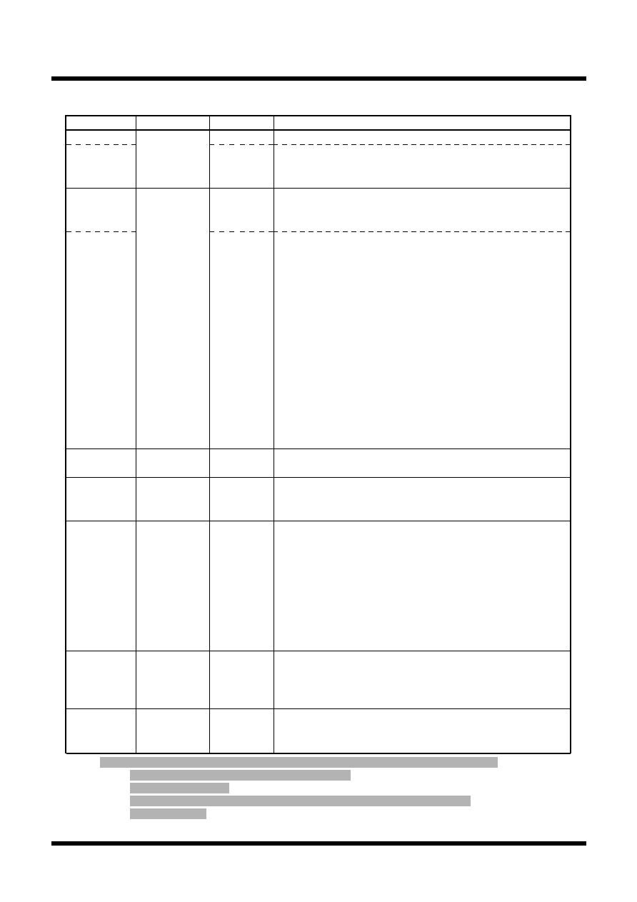
The M16C/62T group products currently supported are listed in Table 1.1.2.
Type No.
Package
Remarks
M30622MCT-XXXFP
M30622ECT-XXXFP
M30622ECTFP
128K bytes
Mask ROM version
One-time PROM version (programming)
One-time PROM version (blank)
100P6S-A
M30622MCV-XXXFP
M30622ECV-XXXFP
M30622ECVFP
M30623MCT-XXXGP
M30623ECT-XXXGP
M30623ECTGP
128K bytes
80P6S-A
Characteristic
5K bytes
5K bytes
M30623MCV-XXXGP
M30623ECV-XXXGP
M30623ECVGP
M30622M8T-XXXFP
M30622M8V-XXXFP
64K bytes
Mask ROM version
85 °C guaranteed version
4K bytes
M30623M4T-XXXGP
M30623M8T-XXXGP
M30623M8V-XXXGP
125 °C guaranteed version (Note 3)
64K bytes
4K bytes
32K bytes
3K bytes
ROM
capacity
RAM
capacity
85 °C guaranteed version
85 °C guaranteed version
85 °C guaranteed version
85 °C guaranteed version
125 °C guaranteed version (Note 3)
125 °C guaranteed version (Note 3)
125 °C guaranteed version (Note 3)
Mask ROM version
Mask ROM version
Mask ROM version
Mask ROM version
Mask ROM version
One-time PROM version (programming)
One-time PROM version (blank)
One-time PROM version (programming)
One-time PROM version (blank)
One-time PROM version (programming)
One-time PROM version (blank)
Table 1.1.2. M16C/62T group
Now: Mar.1999.
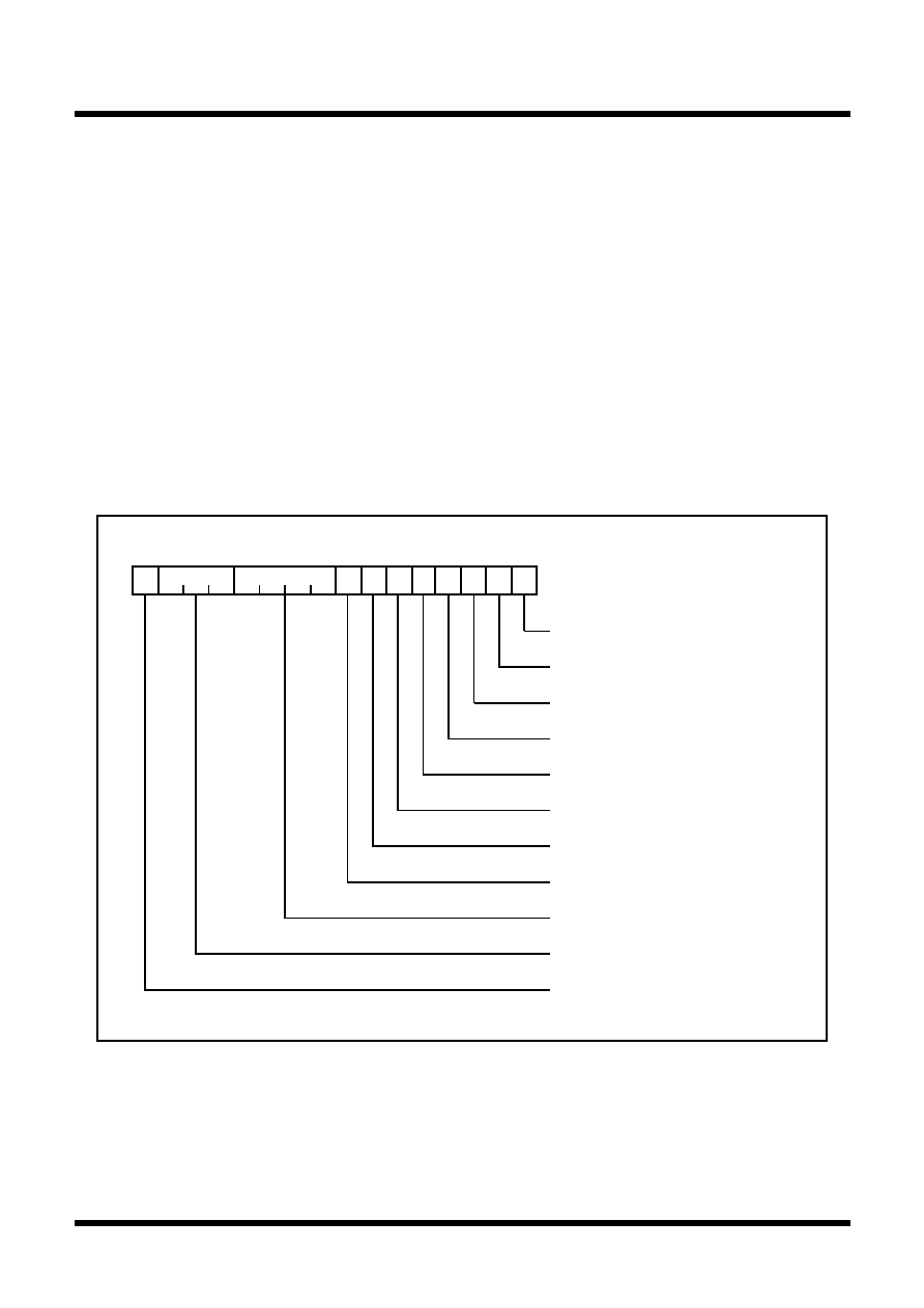
Type No. M30 62 2 M C T XXX FP
Package type
FP : Package 100P6S-A
GP :
80P6S-A
ROM No.
Omitted for blank one-time PROM version
and EPROM version
ROM capacity
4 :
32K bytes
8 :
64K bytes
C : 128K bytes
Memory type
M : Mask ROM version
E : EPROM or one-time PROM version
Shows RAM capacity, pin count, etc
(The value itself has no specific meaning)
M16C Family
M16C/62 Group
Characteristic
T : 85 °C guaranteed version for automobile
V : 125 °C guaranteed version for automobile
Figure 1.1.6. Type No., memory size, and package
Note 1: It may change in the future.
Note 2: Use shipped in blank of one-time PROM version as the trial, development of program.
In case of vehicle-mount test or mass production, use shipped in programming.
Note 3: It is different from 85
°
C guaranteed version on operating ambient temperature and the terms of the
use, pleas inquire.
Tentative Specifications REV.A
Mitsubishi microcomputers
M16C / 62T Group
SINGLE-CHIP 16-BIT CMOS MICROCOMPUTER
S
pecifications in this manual are tentative and subject to change.
Under
development
9
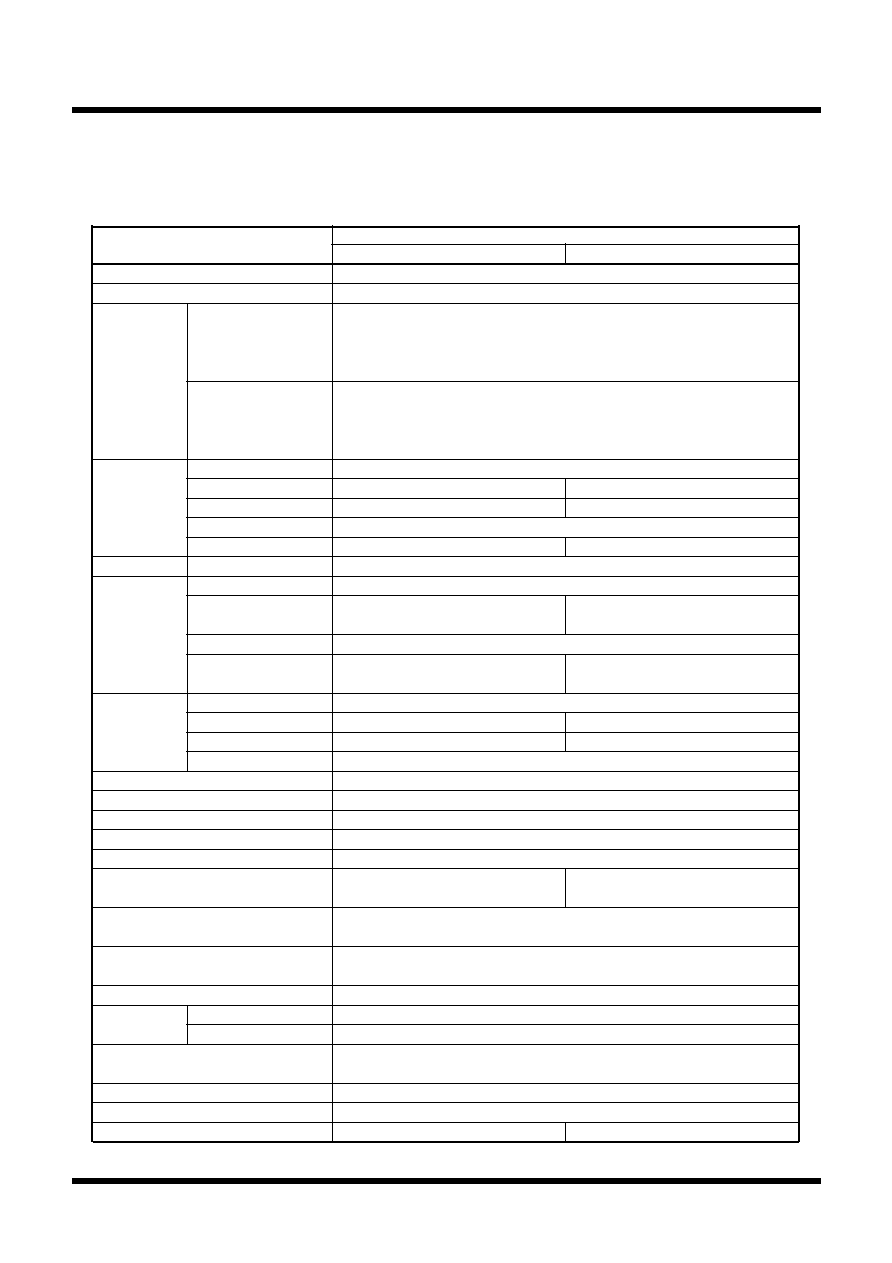
Pin Description
Pin Description
Pin name
V
CC
, V
SS
CNV
SS
____________
RESET
X
IN
X
OUT
BYTE
AV
CC
AV
SS
V
REF
P0
0
to P0
7
D
0
to D
7
P1
0
to P1
7
D
8
to D
15
P2
0
to P2
7
A
0
to A
7
A
0
/D
0
to
A
7
/D
7
A
0
, A
1
/D
0
to A
7
/D
6
P3
0
to P3
7
A
8
to A
15
A
8
/D
7
,
A
9
to A
15
Signal name
Power supply
input
CNV
SS
Reset input
Clock input
Clock output
External data
bus width
select input
Analog power
supply input
Analog power
supply input
Reference
voltage input
I/O port P0
I/O port P1
I/O port P2
I/O port P3
I/O type
Input
Input
Input
Output
Input
Input
Input/output
Input/output
Input/output
Input/output
Input/output
Output
Input/output
Output
Input/output
Input/output
Output
Input/output
Function
Supply 4.2 V to 5.5 V to the V
CC
pin. Supply 0 V to the V
SS
pin.
This pin switches between processor modes. Connect it to the V
SS
pin when operating in single-chip or memory expansion mode.
Connect it to the V
CC
pin when operating in microprocessor mode.
A "L" on this input resets the microcomputer.
These pins are provided for the main clock generating circuit.
Connect a ceramic resonator or crystal between the X
IN
and the
X
OUT
pins. To use an externally derived clock, input it to the X
IN
pin
and leave the X
OUT
pin open.
This pin selects the width of an external data bus. A 16-bit width is
selected when this input is "L"; an 8-bit width is selected when this
input is "H". This input must be fixed to either "H" or "L". When
operating in single-chip mode, connect this pin to V
SS
. In M30623
(80-pin package), the BYTE signal is internally connected to the
CNV
SS
signal.
This pin is a power supply input for the A-D converter. Connect this
pin to V
CC
.
This pin is a power supply input for the A-D converter. Connect this
pin to V
SS
.
This pin is a reference voltage input for the A-D converter.
This is an 8-bit CMOS I/O port. It has an input/output port direction
register that allows the user to set each pin for input or output
individually. When set for input, the user can specify in units of four
bits via software whether or not they are tied to a pull-up resistor.
Pins in this port also function as A-D converter extended input pins
as selected by software when operating in single-chip mode.
When set as a separate bus, these pins input and output data (D
0
D
7
).
This is an 8-bit I/O port equivalent to P0. Pins in this port also
function as external interrupt pins as selected by software.
When set as a separate bus, these pins input and output data (D
8
D
15
).
This is an 8-bit I/O port equivalent to P0. Pins in this port also
function as A-D converter extended input pins as selected by
software when operating in single-chip mode.
These pins output 8 low-order address bits (A
0
A
7
).
If the external bus is set as an 8-bit wide multiplexed bus, these pins
input and output data (D
0
D
7
) and output 8 low-order address bits
(A
0
A
7
) separated in time by multiplexing.
If the external bus is set as a 16-bit wide multiplexed bus, these pins
input and output data (D
0
D
6
) and output address (A
1
A
7
)
separated in time by multiplexing. They also output address (A
0
).
This is an 8-bit I/O port equivalent to P0.
These pins output 8 middle-order address bits (A
8
A
15
).
If the external bus is set as a 16-bit wide multiplexed bus, these pins
input and output data (D
7
) and output address (A
8
) separated in time
by multiplexing. They also output address (A
9
A
15
).
Tentative Specifications REV.A
Mitsubishi microcomputers
M16C / 62T Group
SINGLE-CHIP 16-BIT CMOS MICROCOMPUTER
S
pecifications in this manual are tentative and subject to change.
Under
development
10
Pin Description
Pin Description
Pin name
P4
0
to P4
7
______
______
CS
0
to CS
3
,
A
16
to A
19
P5
0
to P5
7
________ ______
WRL/WR,
_________ _______
WRH/BHE,
RD,
BCLK,
__________
HLDA,
__________
HOLD,
ALE,
________
RDY
P6
0
to P6
7
P7
0
to P7
7
P8
0
to P8
4
,
P8
6
,
P8
7
,
P8
5
P9
0
to P9
7
P10
0
to P10
7
Signal name
I/O port P4
I/O port P5
I/O port P6
I/O port P7
I/O port P8
I/O port P8
5
I/O port P9
I/O port P10
I/O type
Input/output
Output
Output
Input/output
Output
Output
Output
Output
Output
Input
Output
Input
Input/output
Input/output
Input/output
Input/output
Input/output
Input
Input/output
Input/output
Function
This is an 8-bit I/O port equivalent to P0.
______
______
_______
_______
These pins output CS
0
CS
3
signals and A
16
A
19
. CS
0
CS
3
are
chip select signals used to specify an access space. A
16
A
19
are 4
high-order address bits.
This is an 8-bit I/O port equivalent to P0. In single-chip mode, P5
7
in
this port outputs a divide-by-8 or divide-by-32 clock of X
IN
or a clock
of the same frequency as X
CIN
as selected by software.
________
________
______
_______
_____
__________
Output WRL, WRH (WR and BHE), RD, BCLK, HLDA, and ALE
________
_________
_______
______
signals. WRL and WRH, and BHE and WR can be switched using
software control.
________
________
_____
s
WRL, WRH, and RD selected
With a 16-bit external data bus, data is written to even addresses
________
when the WRL signal is "L" and to the odd addresses when the
________
_____
WRH signal is "L". Data is read when RD is "L".
______
_______
_____
s
WR, BHE, and RD selected
______
_____
Data is written when WR is "L". Data is read when RD is "L". Odd
_______
addresses are accessed when BHE is "L". Use this mode when
using an 8-bit external data bus.
__________
While the input level at the HOLD pin is "L", the microcomputer is
__________
placed in the hold state. While in the hold state, HLDA outputs a
"L" level. ALE is used to latch the address. While the input level of
_______
the RDY pin is "L", the microcomputer is in the ready state.
This is an 8-bit I/O port equivalent to P0. Pins in this port also
function as UART0 and UART1 I/O pins as selected by software.
This is an 8-bit I/O port equivalent to P0 (P7
0
and P7
1
are N channel
open-drain output). Pins in this port also function as timer A
0
A
3
,
timer B5 or UART2 I/O pins as selected by software.
P8
0
to P8
4
, P8
6
and P8
7
are I/O ports with the same functions as P0.
Using software, they can be made to function as the I/O pins for
timer A4 and the input pins for external interrupts. P8
6
and P8
7
can
be set using software to function as the I/O pins for a sub clock
generation circuit. In this case, connect a quartz oscillator between
P8
6
(X
COUT
pin) and P8
7
(X
CIN
pin). P8
5
is an input-only port that
_______
_______
also functions for NMI. The NMI interrupt is generated when the
_______
input at this pin changes from "H" to "L". The NMI function cannot be
cancelled using software. The pull-up cannot be set for this pin.
This is an 8-bit I/O port equivalent to P0. Pins in this port also
function as SI/O 3, 4 I/O pins, timer B0B4 input pins, D-A converter
output pins, A-D converter extended input pins, or A-D trigger input
pins as selected by software.
This is an 8-bit I/O port equivalent to P0. Pins in this port also
funciton as A-D converter input pins. Furthermore, P10
4
P10
7
also
function as input pins for the key input interrupt function.
Note 1: In M30623(80-pin package), the following signals do not have the corresponding external pin.
_______
_______
q
P1
0
/D
8
to P1
4
/D
12
, P1
5
/D
13
/INT
3
to P1
7
/D
15
/INT
5
_______
_______
q
P4
4
/CS0 to P4
7
/CS3
________
________
__
___
q
P7
2
/CLK
2
/TA1
OUT
/V, P7
3
/CST
2
/RTS
2
/TA1
IN
/V, P7
4
/TA2
OUT
/W, P7
5
/TA2
IN
/W
q
P9
1
/TB1
IN
/S
IN3
Note 2: The M16C/62T group is not guaranteed to operate in memory expansion and microprocessor modes.
11
Tentative Specifications REV.A
Mitsubishi microcomputers
M16C / 62T Group
SINGLE-CHIP 16-BIT CMOS MICROCOMPUTER
S
pecifications in this manual are tentative and subject to change.
Under
development
Memory
Operation of Functional Blocks
The M16C/62T group accommodates certain units in a single chip. These units include ROM and RAM to
store instructions and data and the central processing unit (CPU) to execute arithmetic/logic operations.
Also included are peripheral units such as timers, serial I/O, D-A converter, DMAC, CRC calculation circuit,
A-D converter, and I/O ports.
The following explains each unit.
Memory
Figure 1.4.1 is a memory map of the M16C/62T group. The address space extends the 1M bytes from
address 00000
16
to FFFFF
16
.
Internal ROM is located as the following, in M30623M4T-XXXGP from address F8000
16
to FFFFF
16
(32K
bytes), in M30622M8T/M8V-XXXFP and M30623M8T/M8V-XXXGP from address F0000
16
to FFFFF
16
(64K bytes), in M30622MCT/MCV-XXXFP and M30623MCT/MCV-XXXGP from address E0000
16
to
FFFFF
16
(128K bytes).
_______
The vector table for fixed interrupts such as the reset and NMI are mapped to FFFDC
16
to FFFFF
16
. The
starting address of the interrupt routine is stored here. The address of the vector table for timer interrupts,
etc., can be set as desired using the internal register (INTB). See the section on interrupts for details.
Internal RAM is located as the following, in M30623M4T-XXXGP from address 00400
16
to 00FFF
16
(3K
bytes), in M30622M8T/M8V-XXXFP and
M30623M8T/M8V-XXXGP from address 00400
16
to 013FF
16
(4K
bytes), in M30622MCT/MCV-XXXFP and M30623MCT/MCV-XXXGP from address 00400
16
to 017FF
16
(5K bytes).
In addition to storing data, the RAM also stores the stack used when calling subroutines and
when interrupts are generated.
The SFR area is mapped to 00000
16
to 003FF
16
. This area accommodates the control registers for
peripheral devices such as I/O ports, A-D converter, serial I/O, and timers, etc. Figures 1.7.1 to 1.7.3 are
location of peripheral unit control registers. Any part of the SFR area that is not occupied is reserved and
cannot be used for other purposes.
The special page vector table is mapped to FFE00
16
to FFFDB
16
. If the starting addresses of subroutines
or the destination addresses of jumps are stored here, subroutine call instructions and jump instructions
can be used as 2-byte instructions, reducing the number of program steps.
In memory expansion mode and microprocessor mode, a part of the spaces are reserved and cannot be
used. For example, in the M30623MCT/MCV-XXXGP, the following spaces cannot be used.
· The space between 01000
16
and 03FFF
16
(Memory expansion and microprocessor modes)
· The space between D0000
16
and D7FFF
16
(Memory expansion mode)
But the M16C/62T group is not guaranteed to operate in memory expansion and microprocessor modes.
Figure 1.4.1. Memory map
SFR area
For details, see Figures
1.7.1 to 1.7.3
Internal RAM area
External area
Internal RAM area
Reset
Watchdog timer
Single step
Address match
BRK instruction
Overflow
Undefined instruction
Special page
vector table
00000
16
00400
16
04000
16
FFFFF
16
FFFDC
16
FFE00
16
DBC
NMI
FFFFF
16
XXXXX
16
YYYYY
16
D0000
16
Type No.
XXXXX
16
YYYYY
16
M30623M4T-XXXGP
M30622M8T/M8V-XXXFP
M30623M8T/M8V-XXXGP
M30622MCT/MCV-XXXFP
M30623MCT/MCV-XXXGP
00FFF
16
F8000
16
013FF
16
F0000
16
017FF
16
E0000
16
Internal reserved area
(Note 1)
Internal reserved area
(Note 1)
Note 1. In memory expansion and microprocessor modes,
can not be used.
Note 2. In memory expansion mode, can not be used.
Note 3. The M16C/62T group is not guaranteed to operate
in memory expansion and microprocessor modes.
12
Tentative Specifications REV.A
Mitsubishi microcomputers
M16C / 62T Group
SINGLE-CHIP 16-BIT CMOS MICROCOMPUTER
S
pecifications in this manual are tentative and subject to change.
Under
development
CPU
Central Processing Unit (CPU)
The CPU has a total of 13 registers shown in Figure 1.5.1. Seven of these registers (R0, R1, R2, R3, A0,
A1, and FB) come in two sets; therefore, these have two register banks.
(1) Data registers (R0, R0H, R0L, R1, R1H, R1L, R2, and R3)
Data registers (R0, R1, R2, and R3) are configured with 16 bits, and are used primarily for transfer and
arithmetic/logic operations.
Registers R0 and R1 each can be used as separate 8-bit data registers, high-order bits as (R0H/R1H),
and low-order bits as (R0L/R1L). In some instructions, registers R2 and R0, as well as R3 and R1 can
use as 32-bit data registers (R2R0/R3R1).
(2) Address registers (A0 and A1)
Address registers (A0 and A1) are configured with 16 bits, and have functions equivalent to those of data
registers. These registers can also be used for address register indirect addressing and address register
relative addressing.
In some instructions, registers A1 and A0 can be combined for use as a 32-bit address register (A1A0).
H
L
b15
b8
b7
b0
R0
(Note)
H
L
b15
b8
b7
b0
R1
(Note)
R2
(Note)
b15
b0
R3
(Note)
b15
b0
A0
(Note)
b15
b0
A1
(Note)
b15
b0
FB
(Note)
b15
b0
Data
registers
Address
registers
Frame base
registers
b15
b0
b15
b0
b15
b0
b15
b0
b0
b19
b0
b19
H
L
Program counter
Interrupt table
register
User stack pointer
Interrupt stack
pointer
Static base
register
Flag register
PC
INTB
USP
ISP
SB
FLG
Note: These registers consist of two register banks.
C
D
Z
S
B
O
I
U
IPL
Figure 1.5.1. Central processing unit register

13
Tentative Specifications REV.A
Mitsubishi microcomputers
M16C / 62T Group
SINGLE-CHIP 16-BIT CMOS MICROCOMPUTER
S
pecifications in this manual are tentative and subject to change.
Under
development
CPU
(3) Frame base register (FB)
Frame base register (FB) is configured with 16 bits, and is used for FB relative addressing.
(4) Program counter (PC)
Program counter (PC) is configured with 20 bits, indicating the address of an instruction to be executed.
(5) Interrupt table register (INTB)
Interrupt table register (INTB) is configured with 20 bits, indicating the start address of an interrupt vector
table.
(6) Stack pointer (USP/ISP)
Stack pointer comes in two types: user stack pointer (USP) and interrupt stack pointer (ISP), each config-
ured with 16 bits.
Your desired type of stack pointer (USP or ISP) can be selected by a stack pointer select flag (U flag).
This flag is located at the position of bit 7 in the flag register (FLG).
(7) Static base register (SB)
Static base register (SB) is configured with 16 bits, and is used for SB relative addressing.
(8) Flag register (FLG)
Flag register (FLG) is configured with 11 bits, each bit is used as a flag. Figure 1.5.2 shows the flag
register (FLG). The following explains the function of each flag:
· Bit 0: Carry flag (C flag)
This flag retains a carry, borrow, or shift-out bit that has occurred in the arithmetic/logic unit.
· Bit 1: Debug flag (D flag)
This flag enables a single-step interrupt.
When this flag is "1", a single-step interrupt is generated after instruction execution. This flag is
cleared to "0" when the interrupt is acknowledged.
· Bit 2: Zero flag (Z flag)
This flag is set to "1" when an arithmetic operation resulted in 0; otherwise, cleared to "0".
· Bit 3: Sign flag (S flag)
This flag is set to "1" when an arithmetic operation resulted in a negative value; otherwise, cleared to "0".
· Bit 4: Register bank select flag (B flag)
This flag chooses a register bank. Register bank 0 is selected when this flag is "0" ; register bank 1 is
selected when this flag is "1".
· Bit 5: Overflow flag (O flag)
This flag is set to "1" when an arithmetic operation resulted in overflow; otherwise, cleared to "0".
· Bit 6: Interrupt enable flag (I flag)
This flag enables a maskable interrupt.
An interrupt is disabled when this flag is "0", and is enabled when this flag is "1". This flag is cleared to
"0" when the interrupt is acknowledged.
14
Tentative Specifications REV.A
Mitsubishi microcomputers
M16C / 62T Group
SINGLE-CHIP 16-BIT CMOS MICROCOMPUTER
S
pecifications in this manual are tentative and subject to change.
Under
development
CPU
· Bit 7: Stack pointer select flag (U flag)
Interrupt stack pointer (ISP) is selected when this flag is "0" ; user stack pointer (USP) is selected
when this flag is "1".
This flag is cleared to "0" when a hardware interrupt is acknowledged or an INT instruction of software
interrupt Nos. 0 to 31 is executed.
· Bits 8 to 11: Reserved area
· Bits 12 to 14: Processor interrupt priority level (IPL)
Processor interrupt priority level (IPL) is configured with three bits, for specification of up to eight
processor interrupt priority levels from level 0 to level 7.
If a requested interrupt has priority greater than the processor interrupt priority level (IPL), the interrupt
is enabled.
· Bit 15: Reserved area
The C, Z, S, and O flags are changed when instructions are executed. See the software manual for
details.
Figure 1.5.2. Flag register (FLG)
Carry flag
Debug flag
Zero flag
Sign flag
Register bank select flag
Overflow flag
Interrupt enable flag
Stack pointer select flag
Reserved area
Processor interrupt priority level
Reserved area
Flag register (FLG)
C
D
Z
S
B
O
I
U
IPL
b0
b15
15
Mitsubishi microcomputers
M16C / 62T Group
SINGLE-CHIP 16-BIT CMOS MICROCOMPUTER
Reset
Figure 1.6.2. Reset sequence
Reset
There are two kinds of resets; hardware and software. In both cases, operation is the same after the reset.
(See "Software Reset" for details of software resets.) This section explains on hardware resets.
When the supply voltage is in the range where operation is guaranteed, a reset is effected by holding the
reset pin level "L" (0.2V
CC
max.) for at least 20 cycles. When the reset pin level is then returned to the "H"
level while main clock is stable, the reset status is cancelled and program execution resumes from the
address in the reset vector table.
Figure 1.6.1 shows the example reset circuit. Figure 1.6.2 shows the reset sequence.
Figure 1.6.1. Example reset circuit
X
IN
Microprocessor
mode
BYTE = "H"
BCLK
FFFFC
16
FFFFD
16
FFFFE
16
Content of reset vector
BCLK 24 cycles
More than 20 cycles are needed
Address
FFFFC
16
Content of reset vector
Address
FFFFE
16
RESET
RD
WR
CS0
RD
WR
CS0
FFFFC
16
Content of reset vector
Address
Single chip
mode
FFFFE
16
("H")
Microprocessor
mode
BYTE = "L"
("H")
Note 1: In M30623(80-pin package), the BYTE signal has no external pin, and is internally connected to
the CNV
SS
signal. Accordingly, in the microprocessor mode, BYTE = CNV
SS
= Vcc.
Note 2: M16C/62T group is not guaranteed to operate in memory expansion and microprocessor modes.
Note 3: M30623(80-pin package) is not provided with the chip select signals (CS0 to CS3).
Vcc
RESET
4.0V
0.8V
0V
5V
0V
5V
Vcc
RESET
Example when Vcc=5V.
More than 20 cycles of X
IN
are needed.
16
Mitsubishi microcomputers
M16C / 62T Group
SINGLE-CHIP 16-BIT CMOS MICROCOMPUTER
Reset
____________
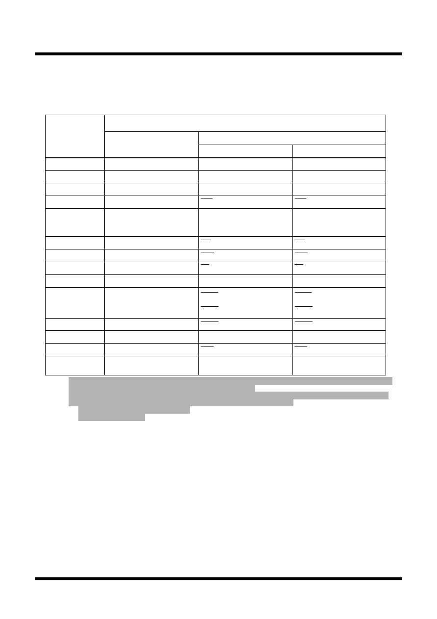
Table 1.6.1 shows the statuses of the other pins while the RESET pin level is "L". Figures 1.6.3 and 1.6.4
show the internal status of the microcomputer immediately after the reset is cancelled.
____________
Table 1.6.1. Pin status when RESET pin level is "L"
Status
CNV
SS
= V
CC
CNV
SS
= V
SS
BYTE = V
SS
(Note 1)
BYTE = V
CC
Pin
name
P0
P1
P2, P3, P4
0
to P4
3
P4
4
P4
5
to P4
7
P5
0
P5
1
P5
2
P5
3
P5
4
P5
5
P5
6
P5
7
P6, P7, P8
0
to P8
4
,
P8
6
, P8
7
, P9, P10
Input port (floating)
Input port (floating)
Input port (floating)
Input port (floating)
Input port (floating)
(pull-up resistor is on)
Input port (floating)
Input port (floating)
Input port (floating)
Input port (floating)
Input port (floating)
Input port (floating)
Input port (floating)
Input port (floating)
Input port (floating)
Data input (floating)
Data input (floating)
Address output (undefined)
BCLK output
ALE output ("L" level is output)
CS0 output ("H" level is output)
WR output ("H" level is output)
RD output ("H" level is output)
RDY input (floating)
Input port (floating)
BCLK output
BHE output (undefined)
HLDA output (The output value
depends on the input to the
HOLD pin)
HOLD input (floating)
Data input (floating)
Address output (undefined)
CS0 output ("H" level is output)
Input port (floating)
(pull-up resistor is on)
Input port (floating)
Input port (floating)
RDY input (floating)
ALE output ("L" level is output)
HOLD input (floating)
HLDA output (The output value
depends on the input to the
HOLD pin)
RD output ("H" level is output)
BHE output (undefined)
WR output ("H" level is output)
Input port (floating)
(pull-up resistor is on)
Note 1: In M30623(80-pin package), the BYTE signal has no external pin, and is internally connected to the CNV
SS
signal.
Accordingly, in the microprocessor mode, BYTE = CNV
SS
= V
CC
.
Note 2: In M30623(80-pin package), Port P1, P4
4
to P4
7
, P7
2
to P7
5
and P9
1
have no external pin, and are internally the
above conditions. After reset, set these ports to one of the following conditions.
· Be output mode, and output "L" level.
· Pull-up resister is on.
17
Mitsubishi microcomputers
M16C / 62T Group
SINGLE-CHIP 16-BIT CMOS MICROCOMPUTER
Reset
Figure 1.6.3. Device's internal status after a reset is cleared
(8)
(9)
(11)
(12)
(13)
(14)
(15)
(16)
(17)
(18)
(19)
(20)
(21)
(22)
(23)
(1)
(0004
16
)···
Processor mode register 0 (Note 1)
(2)
(0005
16
)···
Processor mode register 1
(4)
(0007
16
)···
System clock control register 1
(5)
(0008
16
)···
Chip select control register
(6)
(0009
16
)···
Address match interrupt enable register
(7) Protect register
(3)
(0006
16
)···
System clock control register 0
00
16
(000A
16
)···
(000F
16
)···
Watchdog timer control register
(0010
16
)···
Address match interrupt register 0
(0011
16
)···
(0012
16
)···
(0014
16
)···
Address match interrupt register 1
(0015
16
)···
(0016
16
)···
(002C
16
)···
DMA0 control register
(003C
16
)···
DMA1 control register
(004A
16
)···
Bus collision detection interrupt
(004B
16
)···
DMA0 interrupt control register
(004C
16
)···
DMA1 interrupt control register
(004D
16
)···
Key input interrupt control register
(24) A-D conversion interrupt control register
(004E
16
)···
Data bank register
(000B
16
)···
(10)
(0044
16
)···
INT3 interrupt control register
(0045
16
)···
Timer B5 interrupt control register
(0046
16
)···
Timer B4 interrupt control register
(0047
16
)···
Timer B3 interrupt control register
(0048
16
)···
SI/O4 interrupt control register
(0049
16
)···
SI/O3 interrupt control register
(25)
(26)
(27)
(28)
(29)
(30)
(004F
16
)···
UART2 transmit interrupt control register
(0050
16
)···
UART2 receive interrupt control register
(0051
16
)···
UART0 transmit interrupt control register
(0052
16
)···
UART0 receive interrupt control register
(0053
16
)···
UART1 transmit interrupt control register
(0054
16
)···
UART1 receive interrupt control register
(31)
(32)
(33)
(34)
(39)
(41)
(40)
(35)
(36)
(37)
(38)
(0055
16
)···
Timer A0 interrupt control register
(0056
16
)···
Timer A1 interrupt control register
(0057
16
)···
Timer A2 interrupt control register
(0058
16
)···
Timer A3 interrupt control register
(0059
16
)···
Timer A4 interrupt control register
(005A
16
)···
Timer B0 interrupt control register
(005B
16
)···
Timer B1 interrupt control register
(005C
16
)···
Timer B2 interrupt control register
(005D
16
)···
INT0 interrupt control register
(005E
16
)···
INT1 interrupt control register
(005F
16
)···
INT2 interrupt control register
(45)
(46)
(0348
16
)···
Three-phase PWM control register 0
(0349
16
)···
Three-phase PWM control register 1
(034A
16
)···
Three-phase output buffer register 0
(034B
16
)···
Three-phase output buffer register 1
(43)
(42)
(0340
16
)···
Timer B3,4,5 count start flag
(44)
(47)
(035B
16
)···
Timer B3 mode register
(48)
(035C
16
)···
Timer B4 mode register
(49)
(035D
16
)···
Timer B5 mode register
(50)
(035F
16
)···
Interrupt cause select register
0
0 0
0
0
0
0 1
0
0
1 0 0
1
0 0
0
0
0 0 0
0
0 0
0
1
0 0 0
0 0
0 0
0
00
16
?
U
0 0
?
? ?
?
00
16
00
16
0 0
0
0
00
16
00
16
0 0
0
0
0
0 0
0
0
0 ? 0
0
0 0
0
0
0 ? 0
0 0
0
?
0
0
0
?
0
0
0
?
0
0
0
?
0
0
0 0
0
?
0
0
0 0
0
?
0
0
0
?
0
0
0
?
0
0
0
?
0
0
0
?
0
0
0 0
0
?
0
0
0 0
0
?
0
0
0 0
0
?
0
0
0
?
0
0
0
?
0
0
0
?
0
0
0
?
0
0
0
?
0
0
0
?
0
0
0
?
0
0
0
?
0
0
0
?
0
0
0
?
0
0
0
?
0
0
0
?
0
0
0
?
0
0
0
?
0
0
0
?
0
0
00
16
00
16
00
16
00
16
00
16
0
?
0
0
0
0
0
0
?
0
0
0
0
0
0
?
0
0
0
0
0
0
0
0
0
Note 1 : When the V
CC
level is applied to the CNV
SS
pin, it is 03
16
at a reset.
control register
U
: This bit is the cold start / warm start flag, is set to "0" at power on reset (refer to Page 71).
!
: Nothing is mapped to this bit.
? : Undefined
The content of other registers and RAM is undefined when the microcomputer is reset.
The initial values must therefore be set.
18
Mitsubishi microcomputers
M16C / 62T Group
SINGLE-CHIP 16-BIT CMOS MICROCOMPUTER
Reset
Figure 1.6.4. Device's internal status after a reset is cleared
(03E2
16
)···
Port P0 direction register
(80)
(03E3
16
)···
Port P1 direction register
(81)
(03E6
16
)···
Port P2 direction register
(82)
(03E7
16
)···
Port P3 direction register
(83)
(03EA
16
)···
Port P4 direction register
(84)
(03EB
16
)···
Port P5 direction register
(85)
(03EE
16
)···
Port P6 direction register
(86)
(03EF
16
)···
Port P7 direction register
(87)
(03F2
16
)···
Port P8 direction register
(88)
(03F3
16
)···
Port P9 direction register
(89)
(03F6
16
)···
Port P10 direction register
(90)
(03FC
16
)···
Pull-up control register 0
(91)
(03FD
16
)···
Pull-up control register 1 (Note 1)
(92)
(03FE
16
)···
Pull-up control register 2
(93)
Data registers (R0/R1/R2/R3)
(94)
Frame base register (FB)
(96)
Address registers(A0/A1)
(95)
Interrupt table register (INTB)
(97)
User stack pointer (USP)
(98)
Interrupt stack pointer (ISP)
(99)
Static base register (SB)
(100)
Flag register(FLG)
(101)
(03DC
16
)···
D-A control register
(79)
(0383
16
)···
Trigger select flag
(0384
16
)···
Up-down flag
(58)
(57)
(0396
16
)···
Timer A0 mode register
(59)
(0397
16
)···
Timer A1 mode register
(60)
(0398
16
)···
Timer A2 mode register
(63)
(039B
16
)···
Timer B0 mode register
(64)
(039C
16
)···
Timer B1 mode register
(65)
(039D
16
)···
Timer B2 mode register
(66)
(61)
(0399
16
)···
Timer A3 mode register
(62)
(039A
16
)···
Timer A4 mode register
(0382
16
)···
One-shot start flag
(56)
(03A8
16
)···
UART1 transmit/receive mode register
(70)
(03AC
16
)···
UART1 transmit/receive control register 0
(71)
(03AD
16
)···
UART1 transmit/receive control register 1
(72)
(03B0
16
)···
UART transmit/receive control register 2
(73)
(03B8
16
)···
DMA0 cause select register
(74)
(03BA
16
)···
DMA1 cause select register
(75)
(03A0
16
)···
UART0 transmit/receive mode register
(67)
(03A4
16
)···
UART0 transmit/receive control register 0
(68)
(03A5
16
)···
UART0 transmit/receive control register 1
(69)
(03D4
16
)···
A-D control register 2
(76)
(03D6
16
)···
A-D control register 0
(77)
(03D7
16
)···
A-D control register 1
(78)
UART2 transmit/receive control register 1
UART2 transmit/receive control register 0
Count start flag
(0378
16
)···
(037D
16
)···
(037C
16
)···
(0380
16
)···
00
16
(0381
16
)···
Clock prescaler reset flag
(53)
(54) UART2 transmit/receive mode register
(51)
(52)
(55)
0 0 0 0
0
0 0
0 0
0
0 1 0
1 0 0
00
16
0
0
0
0 0
0
0
0
00
16
00
16
00
16
00
16
00
16
00
16
00
16
00
16
0
?
0 0 0
0 0
0
?
0 0 0
0 0
0
?
0 0 0
0 0
00
16
1 0 0 0
0 0 0 0
0 0 1 0
0 0 0 0
1 0 0 0
0 0 0 0
0 0 1 0
0 0 0 0
00
16
00
16
0
0 0
0
0
0 0
0
0
0
0
00
16
0
?
0 0
0
0
?
?
00
16
00
16
00
16
00
16
00
16
00
16
00
16
0 0 0 0
0 0
00
16
00
16
0
00
16
00
16
00
16
00
16
00
16
0000
16
0000
16
0000
16
0000
16
0000
16
0000
16
0000
16
0000
16
(102)
(103)
(104)
(105)
(03FF
16
)···
Port control register
00
16
SI/O3 control register
(0362
16
)··· 0 1 0 0
0
0 0 0
SI/O4 control register
(0366
16
)··· 0 1 0 0
0
0 0 0
(0377
16
)···
00
16
UART2 special mode register
0
Note 1 : When the V
CC
level is applied to the CNV
SS
pin, it is 02
16
at a reset.
The content of other registers and RAM is undefined when the microcomputer is reset.
The initial values must therefore be set.
!
: Nothing is mapped to this bit.
? : Undefined
19
Mitsubishi microcomputers
M16C / 62T Group
SINGLE-CHIP 16-BIT CMOS MICROCOMPUTER
SFR
Figure 1.7.1. Location of peripheral unit control registers (1)
0000
16
0001
16
0002
16
0003
16
0004
16
0005
16
0006
16
0007
16
0008
16
0009
16
000A
16
000B
16
000C
16
000D
16
000E
16
000F
16
0010
16
0011
16
0012
16
0013
16
0014
16
0015
16
0016
16
0017
16
0018
16
0019
16
001A
16
001B
16
001C
16
001D
16
001E
16
001F
16
0020
16
0021
16
0022
16
0023
16
0024
16
0025
16
0026
16
0027
16
0028
16
0029
16
002A
16
002B
16
002C
16
002D
16
002E
16
002F
16
0030
16
0031
16
0032
16
0033
16
0034
16
0035
16
0036
16
0037
16
0038
16
0039
16
003A
16
003B
16
003C
16
003D
16
003E
16
003F
16
0040
16
0041
16
0042
16
0043
16
0044
16
0045
16
0046
16
0047
16
0048
16
0049
16
004A
16
004B
16
004C
16
004D
16
004E
16
004F
16
0050
16
0051
16
0052
16
0053
16
0054
16
0055
16
0056
16
0057
16
0058
16
0059
16
005A
16
005B
16
005C
16
005D
16
005E
16
005F
16
0060
16
0061
16
0062
16
0063
16
0064
16
0065
16
032A
16
032B
16
032C
16
032D
16
032E
16
032F
16
0330
16
0331
16
0332
16
0333
16
0334
16
0335
16
0336
16
0337
16
0338
16
0339
16
033A
16
033B
16
033C
16
033D
16
033E
16
033F
16
DMA0 control register (DM0CON)
DMA0 source pointer (SAR0)
DMA0 transfer counter (TCR0)
DMA1 control register (DM1CON)
DMA1 source pointer (SAR1)
DMA1 transfer counter (TCR1)
DMA1 destination pointer (DAR1)
Watchdog timer start register (WDTS)
Watchdog timer control register (WDC)
Processor mode register 0 (PM0)
Address match interrupt register 0 (RMAD0)
Address match interrupt register 1 (RMAD1)
Chip select control register (CSR)
System clock control register 0 (CM0)
System clock control register 1 (CM1)
Address match interrupt enable register (AIER)
Protect register (PRCR)
Processor mode register 1(PM1)
Data bank register (DBR)
DMA0 destination pointer (DAR0)
Timer A1 interrupt control register (TA1IC)
UART0 transmit interrupt control register (S0TIC)
Timer A0 interrupt control register (TA0IC)
Timer A2 interrupt control register (TA2IC)
UART0 receive interrupt control register (S0RIC)
UART1 transmit interrupt control register (S1TIC)
UART1 receive interrupt control register (S1RIC)
DMA1 interrupt control register (DM1IC)
DMA0 interrupt control register (DM0IC)
Key input interrupt control register (KUPIC)
A-D conversion interrupt control register (ADIC)
Bus collision detection interrupt control register (BCNIC)
UART2 transmit interrupt control register (S2TIC)
UART2 receive interrupt control register (S2RIC)
INT1 interrupt control register (INT1IC)
Timer B0 interrupt control register (TB0IC)
Timer B2 interrupt control register (TB2IC)
Timer A3 interrupt control register (TA3IC)
INT2 interrupt control register (INT2IC)
INT0 interrupt control register (INT0IC)
Timer B1 interrupt control register (TB1IC)
Timer A4 interrupt control register (TA4IC)
INT3 interrupt control register (INT3IC)
Timer B5 interrupt control register (TB5IC)
Timer B4 interrupt control register (TB4IC)
Timer B3 interrupt control register (TB3IC)
SI/O4 interrupt control register (S4IC)
INT5 interrupt control register (INT5IC)
SI/O3 interrupt control register (S3IC)
INT4 interrupt control register (INT4IC)
20
Mitsubishi microcomputers
M16C / 62T Group
SINGLE-CHIP 16-BIT CMOS MICROCOMPUTER
SFR
Figure 1.7.2. Location of peripheral unit control registers (2)
0380
16
0381
16
0382
16
0383
16
0384
16
0385
16
0386
16
0387
16
0388
16
0389
16
038A
16
038B
16
038C
16
038D
16
038E
16
038F
16
0390
16
0391
16
0392
16
0393
16
0394
16
0395
16
0396
16
0397
16
0398
16
0399
16
039A
16
039B
16
039C
16
039D
16
039E
16
039F
16
03A0
16
03A1
16
03A2
16
03A3
16
03A4
16
03A5
16
03A6
16
03A7
16
03A8
16
03A9
16
03AA
16
03AB
16
03AC
16
03AD
16
03AE
16
03AF
16
03B0
16
03B1
16
03B2
16
03B3
16
03B4
16
03B5
16
03B6
16
03B7
16
03B8
16
03B9
16
03BA
16
03BB
16
03BC
16
03BD
16
03BE
16
03BF
16
0340
16
0341
16
0342
16
0343
16
0344
16
0345
16
0346
16
0347
16
0348
16
0349
16
034A
16
034B
16
034C
16
034D
16
034E
16
034F
16
0350
16
0351
16
0352
16
0353
16
0354
16
0355
16
0356
16
0357
16
0358
16
0359
16
035A
16
035B
16
035C
16
035D
16
035E
16
035F
16
0360
16
0361
16
0362
16
0363
16
0364
16
0365
16
0366
16
0367
16
0368
16
0369
16
036A
16
036B
16
036C
16
036D
16
036E
16
036F
16
0370
16
0371
16
0372
16
0373
16
0374
16
0375
16
0376
16
0377
16
0378
16
0379
16
037A
16
037B
16
037C
16
037D
16
037E
16
037F
16
Timer A1-1 register (TA11)
Timer A2-1 register (TA21)
Dead time timer(DTT)
Timer B2 interrupt occurrence frequency set counter(ICTB2)
Three-phase PWM control register 0(INVC0)
Three-phase PWM control register 1(INVC1)
Three-phase output buffer register 0(IDB0)
Three-phase output buffer register 1(IDB1)
Timer B3 register (TB3)
Timer B4 register (TB4)
Timer B5 register (TB5)
Timer B3, 4, 5 count start flag (TBSR)
Timer B3 mode register (TB3MR)
Timer B4 mode register (TB4MR)
Timer B5 mode register (TB5MR)
Interrupt cause select register (IFSR)
Timer A0 (TA0)
Timer A1 (TA1)
Timer A2 (TA2)
Timer B0 (TB0)
Timer B1 (TB1)
Timer B2 (TB2)
Count start flag (TABSR)
One-shot start flag (ONSF)
Timer A0 mode register (TA0MR)
Timer A1 mode register (TA1MR)
Timer A2 mode register (TA2MR)
Timer B0 mode register (TB0MR)
Timer B1 mode register (TB1MR)
Timer B2 mode register (TB2MR)
Up-down flag (UDF)
Timer A3 (TA3)
Timer A4 (TA4)
Timer A3 mode register (TA3MR)
Timer A4 mode register (TA4MR)
Trigger select register (TRGSR)
Clock prescaler reset flag (CPSRF)
UART0 transmit/receive mode register (U0MR)
UART0 transmit buffer register (U0TB)
UART0 receive buffer register (U0RB)
UART1 transmit/receive mode register (U1MR)
UART1 transmit buffer register (U1TB)
UART1 receive buffer register (U1RB)
UART0 bit rate generator (U0BRG)
UART0 transmit/receive control register 0 (U0C0)
UART0 transmit/receive control register 1 (U0C1)
UART1 bit rate generator (U1BRG)
UART1 transmit/receive control register 0 (U1C0)
UART1 transmit/receive control register 1 (U1C1)
DMA1 request cause select register (DM1SL)
DMA0 request cause select register (DM0SL)
CRC data register (CRCD)
CRC input register (CRCIN)
SI/O3 transmit/receive register (S3TRR)
SI/O4 transmit/receive register (S4TRR)
SI/O3 control register (S3C)
SI/O3 bit rate generator (S3BRG)
SI/O4 bit rate generator (S4BRG)
SI/O4 control register (S4C)
UART2 special mode register (U2SMR)
UART2 receive buffer register (U2RB)
UART2 transmit buffer register (U2TB)
UART2 transmit/receive control register 0 (U2C0)
UART2 transmit/receive mode register (U2MR)
UART2 transmit/receive control register 1 (U2C1)
UART2 bit rate generator (U2BRG)
UART transmit/receive control register 2 (UCON)
Timer A4-1 register (TA41)
21
Mitsubishi microcomputers
M16C / 62T Group
SINGLE-CHIP 16-BIT CMOS MICROCOMPUTER
SFR
Figure 1.7.3. Location of peripheral unit control registers (3)
03C0
16
03C1
16
03C2
16
03C3
16
03C4
16
03C5
16
03C6
16
03C7
16
03C8
16
03C9
16
03CA
16
03CB
16
03CC
16
03CD
16
03CE
16
03CF
16
03D0
16
03D1
16
03D2
16
03D3
16
03D4
16
03D5
16
03D6
16
03D7
16
03D8
16
03D9
16
03DA
16
03DB
16
03DC
16
03DD
16
03DE
16
03DF
16
03E0
16
03E1
16
03E2
16
03E3
16
03E4
16
03E5
16
03E6
16
03E7
16
03E8
16
03E9
16
03EA
16
03EB
16
03EC
16
03ED
16
03EE
16
03EF
16
03F0
16
03F1
16
03F2
16
03F3
16
03F4
16
03F5
16
03F6
16
03F7
16
03F8
16
03F9
16
03FA
16
03FB
16
03FC
16
03FD
16
03FE
16
03FF
16
A-D register 7 (AD7)
A-D register 0 (AD0)
A-D register 1 (AD1)
A-D register 2 (AD2)
A-D register 3 (AD3)
A-D register 4 (AD4)
A-D register 5 (AD5)
A-D register 6 (AD6)
Port P0 (P0)
Port P0 direction register (PD0)
Port P1 (P1)
Port P1 direction register (PD1)
Port P2 (P2)
Port P2 direction register (PD2)
Port P3 (P3)
Port P3 direction register (PD3)
Port P4 (P4)
Port P4 direction register (PD4)
Port P5 (P5)
Port P5 direction register (PD5)
Port P6 (P6)
Port P6 direction register (PD6)
Port P7 (P7)
Port P7 direction register (PD7)
Port P8 (P8)
Port P8 direction register (PD8)
Port P9 (P9)
Port P9 direction register (PD9)
Port P10 (P10)
Port P10 direction register (PD10)
Pull-up control register 0 (PUR0)
Pull-up control register 1 (PUR1)
Pull-up control register 2 (PUR2)
A-D control register 0 (ADCON0)
A-D control register 1 (ADCON1)
D-A register 0 (DA0)
D-A register 1 (DA1)
D-A control register (DACON)
A-D control register 2 (ADCON2)
Port control register (PCR)
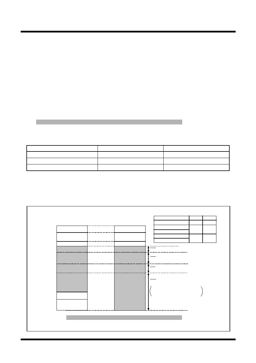
22
Tentative Specifications REV.A
Mitsubishi microcomputers
M16C / 62T Group
SINGLE-CHIP 16-BIT CMOS MICROCOMPUTER
S
pecifications in this manual are tentative and subject to change.
Under
development
Memory Space Expansion Functions
Memory Space Expansion Features
Here follows the description of the memory space expansion function.
With the processor running in memory expansion mode or in microprocessor mode, the memory space
expansion features provide the means of expanding the accessible space. The memory space expansion
features run in one of the three modes given below.
(1) Normal mode (no expansion)
(2) Memory space expansion mode 1 (to be referred as expansion mode 1)
(3) Memory space expansion mode 2 (to be referred as expansion mode 2)
Use bits 5 and 4 (PM15, PM14) of processor mode register 1 to select a desired mode. The external
memory area the chip select signal indicates is different in each mode so that the accessible memory space
varies. Table 1.8.1 shows how to set individual modes and corresponding accessible memory spaces. For
external memory area the chip select signal indicates, see Table 1.12.1 on page 33.
But M30623 (80-pin package) is not provided with the output pin for the chip select signal. And, the M16C/62T group
is not guaranteed to operate in memory expansion and microprocessor modes.
Table 1.8.1. The way of setting memory space expansion modes and corresponding memory spaces
Expansion mode
How to set PM15 and PM14
Accessible memory space
Normal mode (no expansion)
0, 0
Up to 1M byte
Expansion mode 1
1, 0
Up to 1.2M bytes
Expansion mode 2
1, 1
Up to 4M bytes
Here follows the description of individual modes.
(1) Normal mode (a mode with memory not expanded)
`Normal mode' means a mode in which memory is not expanded.
Figure 1.8.1 shows the memory maps and the chip select areas in normal mode.
Figure 1.8.1. The memory maps and the chip select areas in normal mode
Microprocessor mode
SFR area
Internal RAMarea
External area
Internal area reserved
00000
16
00400
16
XXXXX
16
YYYYY
16
FFFFF
16
D0000
16
08000
16
Memory expansion mode
SFR area
Internal RAM area
External area
Internal ROM area
Internal area reserved
Internal area reserved
CS3
(16K bytes)
CS2
(128K bytes)
CS1
(32K bytes)
CS0
Memory expansion mode: 640K bytes
Microprocessor mode: 832K bytes
28000
16
30000
16
04000
16
Normal mode (memory area = 1M bytes for PM15 = 0, PM14 = 0)
Type No.
XXXXX
16
YYYYY
16
M30623M4T-XXXGP
M30622M8T/M8V-XXXFP
M30623M8T/M8V-XXXGP
M30622MCT/MCV-XXXFP
M30623MCT/MCV-XXXGP
00FFF
16
F8000
16
013FF
16
F0000
16
017FF
16
E0000
16
Note 1. M30623(80-pin package) is not provided with the output pins for chip select signals.
Note 2. The M16C/62T group is not guaranteed to operatein memory expansion and microprocessor modes.
Note 3. The memory maps in single-chip mode are omitted.
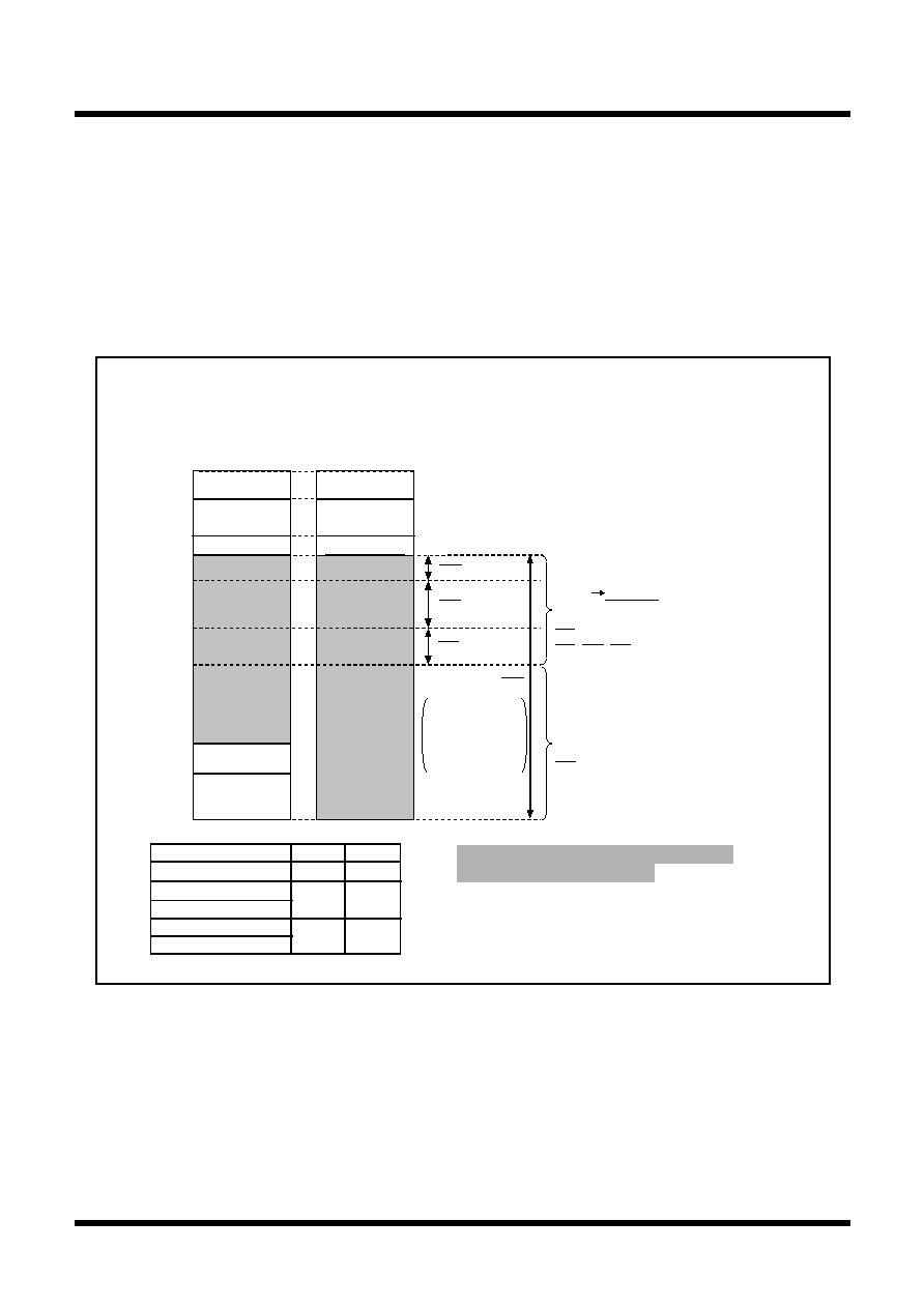
23
Tentative Specifications REV.A
Mitsubishi microcomputers
M16C / 62T Group
SINGLE-CHIP 16-BIT CMOS MICROCOMPUTER
S
pecifications in this manual are tentative and subject to change.
Under
development
Memory Space Expansion Functions
(2) Expansion mode 1
In this mode, the memory space can be expanded by 176K bytes in addition to that in normal mode.
Figure 1.8.2 shows the memory location and chip select area in expansion mode 1.
_______
_______
_______
In accessing data in expansion mode 1, CS3, CS2, and CS1 go active in the area from 04000
16
through
_______
2FFFF
16
; in fetching a program, CS0 goes active. That is, the address space is expanded by using the
________
_______
_______
area from 04000
16
through 2FFFF
16
(176K bytes) appropriately for accessing data (CS3, CS2, CS1)
_______
and fetching a program (CS0).
Figure 1.8.2. Memory location and chip select area in expansion mode 1
Microprocessor
mode
SFR area
Internal RAM
area
External
area
Internal area reserved
00000
16
00400
16
XXXXX
16
YYYYY
16
FFFFF
16
D0000
16
08000
16
Memory
expansion mode
SFR area
Internal RAM
area
External area
Internal ROM
area
Internal area reserved
Internal area reserved
CS3
(16K bytes)
CS2
(128 Kbytes)
CS1
(32K bytes)
28000
16
30000
16
04000
16
Expansion mode 1 (memory space = 1.2M bytes for PM15 = 1, PM14 = 0)
CS0
Memory expansion
mode:
816K bytes
Microprocessor mode:
1008K bytes
04000
16
to
2FFFF
16
30000
16
to
FFFFF
16
176K bytes
= the extent of memory expanded
CS0:active both in fetching a program
and in accessing data
CS0:active in fetching a program
CS1, CS2, CS3:active in accessing data
Type No.
XXXXX
16
YYYYY
16
M30623M4T-XXXGP
M30622M8T/M8V-XXXFP
M30623M8T/M8V-XXXGP
M30622MCT/MCV-XXXFP
M30623MCT/MCV-XXXGP
00FFF
16
F8000
16
013FF
16
F0000
16
017FF
16
E0000
16
Note 1. M30623(80-pin package) is not provided with the
output pin for the chip select signal.
Note 2. The M16C/62T group is not guaranteed to operate
in memory expansion and microprocessor modes.
Note 3. The memory maps in single-chip mode are omitted.
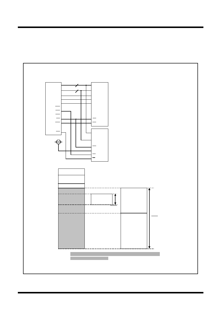
24
Tentative Specifications REV.A
Mitsubishi microcomputers
M16C / 62T Group
SINGLE-CHIP 16-BIT CMOS MICROCOMPUTER
S
pecifications in this manual are tentative and subject to change.
Under
development
Memory Space Expansion Functions
An example of connecting the MCU with external memories in expansion mode 1
(An example of using M30622MC in microprocessor mode)
SFR area
Internal RAM
area
External area
Internal area reserved
00000
16
00400
16
017FF
16
FFFFF
16
D0000
16
08000
16
CS2
(128K bytes)
28000
16
30000
16
04000
16
CS0
SRAM
(128K bytes)
Flash
ROM
(1M byte)
Usable for
programs only
Usable both for
programs and
for data
(1008K bytes)
Usable for
data only
17
8
M30622MC
D0 to D7
A0 to A16
A17
A19
RD
WR
CS1
CS2
CS3
CS0
A18
1M byte flash ROM
D0 to D7
A0 to A16
A17
A18
A19
OE
CS
128K bytes SRAM
DQ0 to
DQ7
A0 to A16
S2
W
OE
S1
Note 1. M30623(80-pin package) is not provided with the output pin
for the chip select signal.
Note 2. The M16C/62T group is not guaranteed to operate
in memory expansion and microprocessor modes.
A connection example
Figure 1.8.3 shows a connection example of the MCU with the external memories in expansion mode 1.
_______
_______
In this example, CS0 is connected with a 1-M byte flash ROM and CS2 is connected with a 128-K byte
SRAM.
Figure 1.8.3. External memory connect example in expansion mode 1
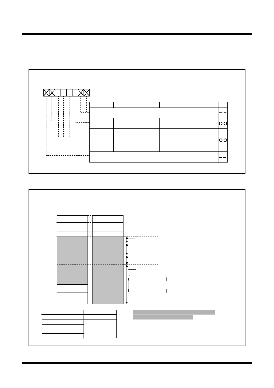
25
Tentative Specifications REV.A
Mitsubishi microcomputers
M16C / 62T Group
SINGLE-CHIP 16-BIT CMOS MICROCOMPUTER
S
pecifications in this manual are tentative and subject to change.
Under
development
Memory Space Expansion Functions
(3) Expansion mode 2
In expansion mode 2, the data bank register (0000B
16
) goes effective. Figure 1.8.4 shows the data bank
register.
Figure 1.8.4. Data bank register
Data bank register
Symbol
Address
When reset
DBR
000B
16
00
16
Bit name
Description
Bit symbol
W
R
b7
b6
b5
b4
b3
b2
b1
b0
OFS
Offset bit
0: Not offset
1: Offset
BSR
Bank selection bits
0 0 0: Bank 0
0 0 1: Bank 1
0 1 0: Bank 2
0 1 1: Bank 3
1 0 0: Bank 4
1 0 1: Bank 5
1 1 0: Bank 6
1 1 1: Bank 7
Nothing is assigned.
In an attempt to write to these bits, write "0". The value, if read, turns out to be "0".
Nothing is assigned.
In an attempt to write to these bits, write "0". The value, if read, turns out to be "0".
b5 b4 b3
b5 b4 b3
Microprocessor
mode
SFR area
Internal RAM area
External area
Internal area reserved
00000
16
00400
16
XXXXX
16
YYYYY
16
FFFFF
16
D0000
16
08000
16
Memory
expansion mode
SFR are
a
Internal RAM area
External area
Internal ROM area
Internal area reserved
Internal area reserved
CS3
(16K bytes)
CS2
(128K bytes)
CS1
(96K bytes)
28000
16
40000
16
04000
16
Expansion mode 2 (memory space = 4M bytes for PM15 = 1, PM14 = 1)
CS0
Addresses from 40000
16
through BFFFF
16
Bank 7 in fetching a program
A bank selected by use of the bank selection
bits in accessing data
Addresses from C0000
16
through FFFFF
16
Bank 7 invariably
Bank number is output to CS3 to CS1
Memory expansion mode:
512K bytes x 7banks +
256K bytes
Microprocessor mode:
512K bytes x 8banks
Type No.
XXXXX
16
YYYYY
16
M30623M4T-XXXGP
M30622M8T/M8V-XXXFP
M30623M8T/M8V-XXXGP
M30622MCT/MCV-XXXFP
M30623MCT/MCV-XXXGP
00FFF
16
F8000
16
013FF
16
F0000
16
017FF
16
E0000
16
Note 1. M30623(80-pin package) is not provided with the
output pin for the chip select signal.
Note 2. The M16C/62T group is not guaranteed to operate
in memory expansion and microprocessor modes.
Note 3. The memory maps in single-chip mode are omitted.
Figure 1.8.5. Memory location and chip select area in expansion mode 2
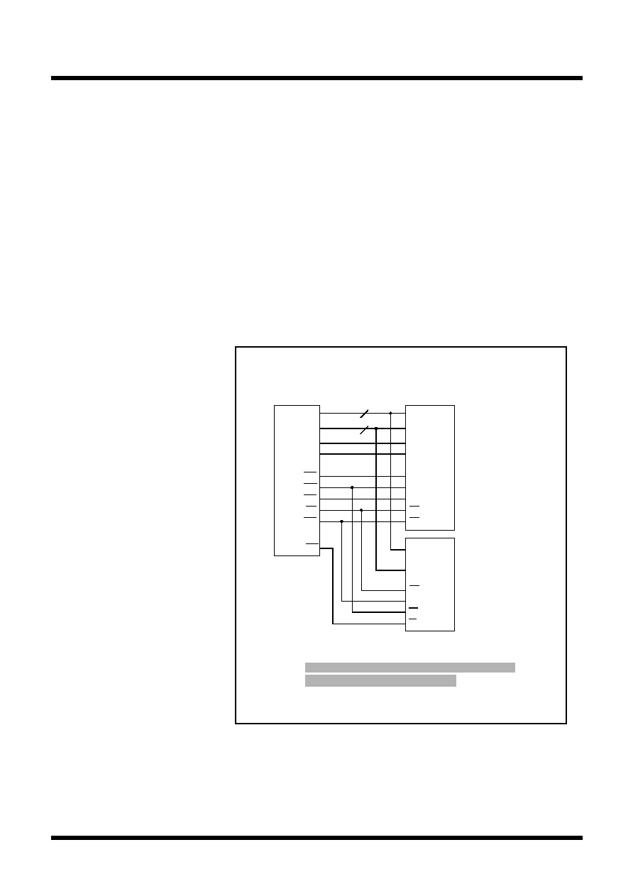
26
Tentative Specifications REV.A
Mitsubishi microcomputers
M16C / 62T Group
SINGLE-CHIP 16-BIT CMOS MICROCOMPUTER
S
pecifications in this manual are tentative and subject to change.
Under
development
Memory Space Expansion Functions
The data bank register is made up of the bank selection bits (bits 5 through 3) and the offset bit (bit 2). The
bank selection bits are used to set a bank number for accessing data lying between 40000
16
and
BFFFF
16
. Assigning 1 to the offset bit provides the means to set offsets covering 40000
16
.
Figure 1.8.5 shows the memory location and chip select areas in expansion mode 2.
_______
The area relevant to CS0 ranges from 40000
16
through FFFFF
16
. As for the area from 40000
16
through
_______
BFFFF
16
, the bank number set by use of the bank selection bits are output from the output terminals CS3
_______
_______
_______
- CS1 only in accessing data. In fetching a program, bank 7 (111
2
) is output from CS3 - CS1. As for the
_______
_______
area from C0000
16
through FFFFF
16
, bank 7 (111
2
) is output from CS3 - CS1 without regard to accessing
data or to fetching a program.
_______
_______
_______
In accessing an area irrelevant to CS0, a chip select signal CS3 (4000
16
- 7FFF
16
), CS2 (8000
16
-
_______
27FFF
16
), and CS1 (28000
16
- 3FFFF
16
) is output depending on the address as in the past.
Figure 1.8.6 shows an example of connecting the MCU with a 4-M byte ROM and to a 128-K byte SRAM.
_______
_______
_______
_______
Connect the chip select of 4-M byte ROM with CS0. Connect M16C's CS3, CS2, and CS1 with address
inputs A21, A20, and A19 respectively. Connect M16C's output A19 with address input A18. Figure 1.8.7
shows the relationship between addresses of the 4-M byte ROM and those of M16C.
An example of connecting the MCU with
external memories in expansion mode 2
(M30622MC, Microprocessor mode)
17
8
M30622MCT-XXXFP
D0 to D7
A0 to A16
A17
RD
WR
CS1
CS2
CS3
CS0
A19
4-M byte ROM
D0 to D7
A0 to A16
A17
A18
A19
OE
CS
128-K byte SRAM
DQ0 to
DQ7
A0 to A16
S2
W
OE
S1
A20
A21
Note 1. If only one chip select terminal (S1 or S2) is present,
decoding by use of an external circuit is required.
Note 2. M30623(80-pin package) is not provided with the
output pin for the chip select signal.
Note 3. The M16C/62T group is not guaranteed to operate
in memory expansion and microprocessor modes.
With no offsets effected,
banks switch from one 512-K
byte segment to another
512-K byte segment. Bank
selection bits need to be
changed in dealing with data
lying across the boundary
between banks every time a
bank switches to another.
Assigning 1 to the offset bit
brings about offsets covering
40000
16
so that data can be
accessed without changing
the bank selection bits. For
instance, accessing 80000
16
of bank 0 with offsets ef-
fected causes the output
bank number to turn to 1, and
AD19 is inverted to be out-
put; this results in accessing
40000
16
of bank 1.
O n t h e o t h e r h a n d , t h e
SRAM's chip select assumes
_______
that CS0=1 (not selected)
_______
and CS2=0 (selected), so
_______
connect CS0 with S2 and
_______
____
CS2 with S1. If the SRAM
doesn't have a bipolar chip
select input terminal, decode
_______
_______
CS0 and CS2 externally.
Figure 1.8.6. An example of connecting the MCU with external
memories in expansion mode 2
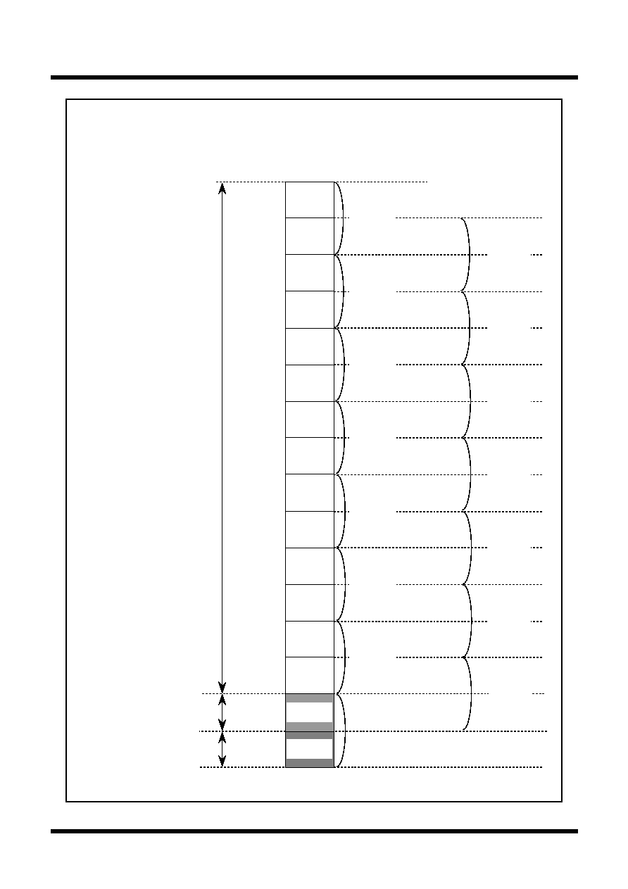
27
Tentative Specifications REV.A
Mitsubishi microcomputers
M16C / 62T Group
SINGLE-CHIP 16-BIT CMOS MICROCOMPUTER
S
pecifications in this manual are tentative and subject to change.
Under
development
Memory Space Expansion Functions
000000
080000
100000
180000
200000
280000
380000
3FFFFF
ROM address
M16C address
40000
BFFFF
40000
BFFFF
3C0000
340000
2C0000
240000
1C0000
140000
0C0000
040000
Bank 0
Bank 1
40000
BFFFF
40000
BFFFF
Bank 1
Bank 2
40000
BFFFF
40000
BFFFF
Bank 2
Bank 3
40000
BFFFF
40000
BFFFF
Bank 3
Bank 4
40000
BFFFF
40000
BFFFF
Bank 4
Bank 5
40000
BFFFF
40000
BFFFF
Bank 5
Bank 6
40000
BFFFF
40000
BFFFF
Bank 6
40000
Bank 7
C0000
FFFFF
7FFFF
Data area
Program/
data area
Areas used for data only
000000
16
to
380000
16
Area commonly used for data
and programs
380000
16
to 3BFFFF
16
Area commonly used for data
and programs
3C0000
16
to 3FFFFF
16
Address area map of 4-M byte ROM
Offset bit = 0
Offset bit = 1
300000
Program/
data area
Data area
Bank 0
Figure 1.8.7. Relationship between addresses on 4-M byte ROM and those on M16C

28
Mitsubishi microcomputers
M16C / 62T Group
SINGLE-CHIP 16-BIT CMOS MICROCOMPUTER
Software Reset
Writing "1" to bit 3 of the processor mode register 0 (address 0004
16
) applies a (software) reset to the
microcomputer. A software reset has almost the same effect as a hardware reset. The contents of internal
RAM are preserved.
Software Reset
Processor Mode
(1) Types of Processor Mode
One of three processor modes can be selected: single-chip mode, memory expansion mode, and micro-
processor mode. The functions of some pins, the memory map, and the access space differ according to
the selected processor mode.
But M16C/62T group is not guaranteed to operate in memory expansion and microprocessor modes.
· Single-chip mode
In single-chip mode, only internal memory space (SFR, internal RAM, and internal ROM) can be
accessed. Ports P0 to P10 can be used as programmable I/O ports or as I/O ports for the internal
peripheral functions.
· Memory expansion mode
In memory expansion mode, external memory can be accessed in addition to the internal memory
space (SFR, internal RAM, and internal ROM).
In this mode, some of the pins function as the address bus, the data bus, and as control signals. The
number of pins assigned to these functions depends on the bus and register settings. (See "Bus
Settings" for details.)
· Microprocessor mode
In microprocessor mode, the SFR, internal RAM, and external memory space can be accessed. The
internal ROM area cannot be accessed.
In this mode, some of the pins function as the address bus, the data bus, and as control signals. The
number of pins assigned to these functions depends on the bus and register settings. (See "Bus
Settings" for details.)
(2) Setting Processor Modes
The processor mode is set using the CNV
SS
pin and the processor mode bits (bits 1 and 0 at address
0004
16
). Do not set the processor mode bits to "10
2
".
Regardless of the level of the CNV
SS
pin, changing the processor mode bits selects the mode. Therefore,
never change the processor mode bits when changing the contents of other bits. Also do not attempt to
shift to or from the microprocessor mode within the program stored in the internal ROM area.
· Applying V
SS
to CNV
SS
pin
The microcomputer begins operation in single-chip mode after being reset. Memory expansion mode
is selected by writing "01
2
" to the processor mode is selected bits.
· Applying V
CC
to CNV
SS
pin
The microcomputer starts to operate in microprocessor mode after being reset.
Figure 1.9.1 shows the processor mode register 0 and 1.
Figure 1.10.1 shows the memory maps applicable for each of the modes when memory area dose not be
expanded (normal mode).
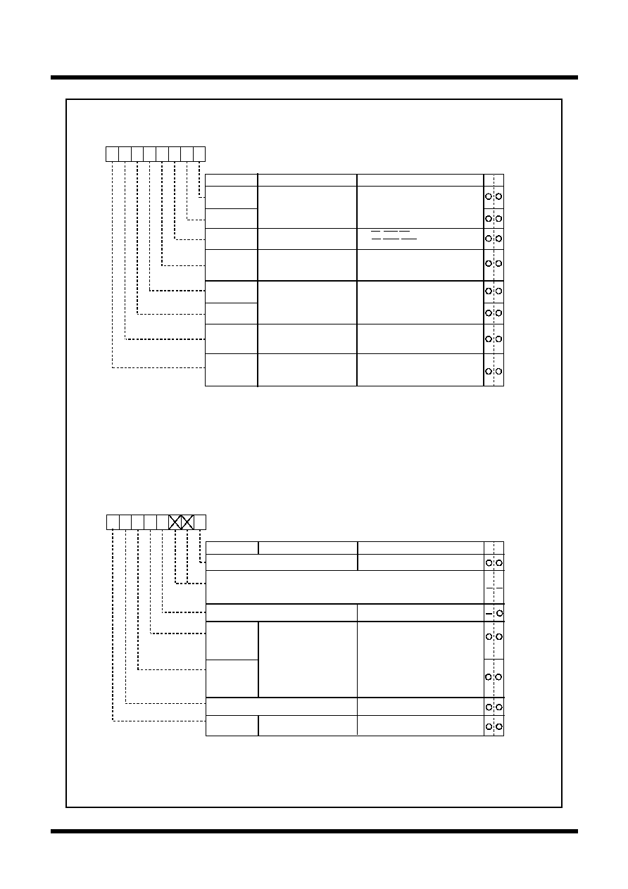
Mitsubishi microcomputers
M16C / 62T Group
SINGLE-CHIP 16-BIT CMOS MICROCOMPUTER
29
Processor Mode
Figure 1.9.1. Processor mode register 0 and 1
Processor mode register 0 (Note 1)
Symbol
Address
When reset
PM0
0004
16
00
16
(Note 2)
Bit name
Function
Bit symbol
W
R
b7
b6
b5
b4
b3
b2
b1
b0
0 0: Single-chip mode
0 1: Memory expansion mode
1 0: Inhibited
1 1: Microprocessor mode
b1 b0
PM03
PM01
PM00
Processor mode bit
PM02
R/W mode select bit
0 : RD,BHE,WR
1 : RD,WRH,WRL
Software reset bit
The device is reset when this bit is set
to "1". The value of this bit is "0" when
read.
PM04
0 0 : Multiplexed bus is not used
0 1 : Allocated to CS2 space
1 0 : Allocated to CS1 space
1 1 : Allocated to entire space (Note4)
b5 b4
Multiplexed bus space
select bit
PM05
PM06
PM07
Port P4
0
to P4
3
function
select bit (Note 3)
0 : Address output
1 : Port function
(Address is not output)
BCLK output disable bit
0 : BCLK is output
1 : BCLK is not output
(Pin is left floating)
Processor mode register 1 (Note 1)
Symbol
Address
When reset
PM1
0005
16
00000XX0
2
Bit name
Function
Bit symbol
W
R
b7
b6
b5
b4
b3
b2
b1
b0
Nothing is assigned.
In an attempt to write to these bits, write "0". The value, if read, turns
out to be
indeterminate.
Reserved bit
Must always be set to "0"
0
PM17
Wait bit
0 : No wait state
1 : Wait state inserted
Memory area
expansion bit (Note 2)
0 0 : Normal mode
(Do not expand)
0 1 : Inhibited
1 0 : Memory area expansion
mode 1
1 1 : Memory area expansion
mode 2
b5 b4
PM15
PM14
Reserved bit
Must always be set to "0"
0
0
Note 1: Set bit 1 of the protect register (address 000A
16
) to "1" when writing new values to this register.
Note 2: If the V
CC
voltage is applied to the CNV
SS
, the value of this register when reset is 03
16
.
(PM00 and PM01 both are set to "1".)
Note 3: Valid in microprocessor and memory expansion modes.
Note 4: If the entire space is of multiplexed bus in memory expansion mode, choose an 8-bit width.
The processor operates using the separate bus after reset is revoked, so the entire space multiplexed
bus cannot be chosen in microprocessor mode. The higher-order address becomes a port if the entire
space multiplexed bus is chosen, so only 256 bytes can be used in each chip select.
Note 5: The M16C/62T group is not guaranteed to operate in memory expansion and microprocessor modes.
Note 1: Set bit 1 of the protect register (address 000A
16
) to "1" when writing new values to this register.
Note 2: With the processor running in memory expansion mode or in microprocessor mode, setting this
bit provides the means of expanding the external memory area. (Normal mode: up to 1M byte,
expansion mode 1: up to 1.2 M bytes, expansion mode 2: up to 4M bytes)
For details, see "Memory space expansion functions".
Note 3: The M16C/62T group is not guaranteed to operate in memory expansion and microprocessor modes.
Reserved bit
Must always be set to "0"
Reserved bit
Must always be set to "0"
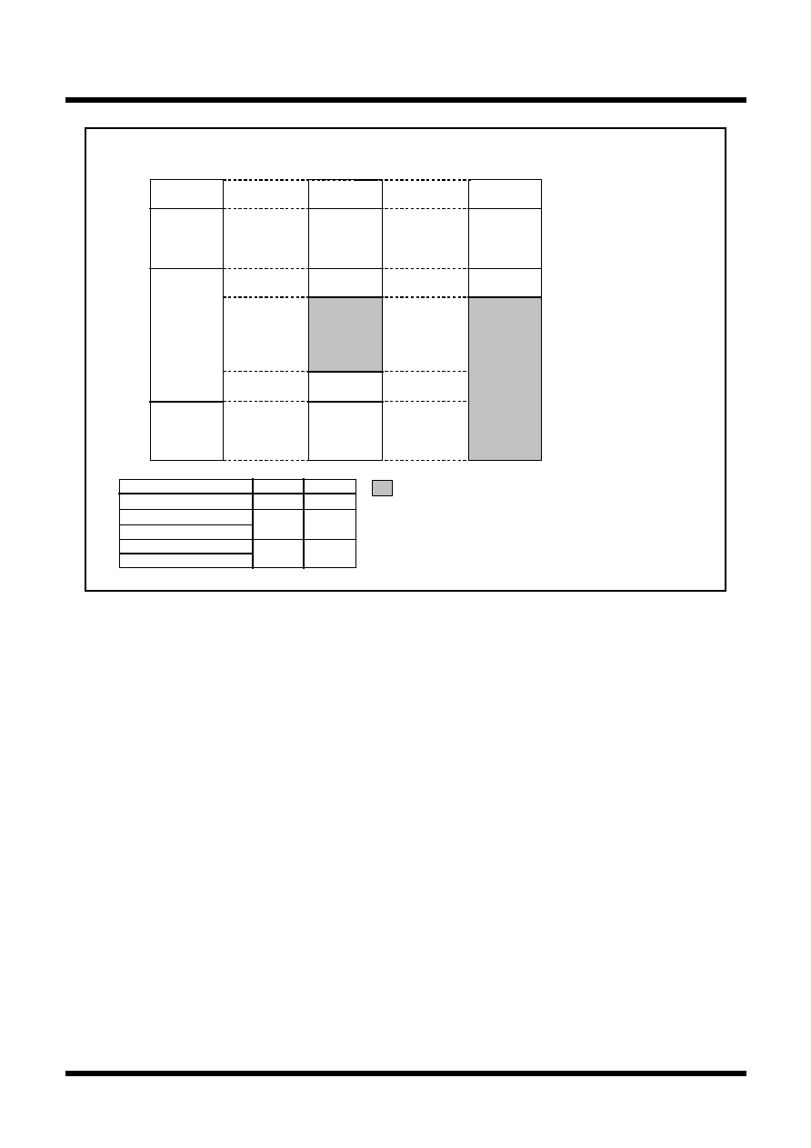
30
Mitsubishi microcomputers
M16C / 62T Group
SINGLE-CHIP 16-BIT CMOS MICROCOMPUTER
Single-chip mode
SFR area
Internal
RAM area
Inhibited
Internal
ROM area
Microprocessor mode
SFR area
Internal
RAM area
External
area
Internally
reserved area
00000
16
00400
16
XXXXX
16
YYYYY
16
FFFFF
16
D0000
16
External area : Accessing this area allows the user to
access a device connected externally
to the microcomputer.
04000
16
Memory expansion mode
SFR area
Internal
RAM area
External
area
Internal
ROM area
Internally
reserved area
Internally
reserved area
Note: The M16C/62T group is not guaranteed to operate
in memory expansion and microprocessor modes.
Type No.
XXXXX
16
YYYYY
16
M30623M4T-XXXGP
M30622M8T/M8V-XXXFP
M30623M8T/M8V-XXXGP
M30622MCT/MCV-XXXFP
M30623MCT/MCV-XXXGP
00FFF
16
F8000
16
013FF
16
F0000
16
017FF
16
E0000
16
Processor Mode
Figure 1.10.1. Memory maps in each processor mode (without memeory area expansion, normal mode)
Mitsubishi microcomputers
M16C / 62T Group
SINGLE-CHIP 16-BIT CMOS MICROCOMPUTER
31
Note 1: In M30623(80-pin package), the external data bus width cannot be switched (be fixed 8 bits).
Bus Settings
The BYTE pin and bits 4 to 6 of the processor mode register 0 (address 0004
16
) are used to change the bus
settings. In M30623(80-pin package), the BYTE signal has no external pin, and is internally connected to
the CNV
SS
signal. Accordingly, the external data bus width can be used only 8 bits.
M16C/62T group is not guaranteed to operate in memory expansion and microprocessor modes.
Table 1.11.1 shows the factors used to change the bus settings.
(1) Selecting external address bus width
The address bus width for external output in the 1M bytes of address space can be set to 16 bits (64K
bytes address space) or 20 bits (1M bytes address space). When bit 6 of the processor mode register 0
is set to "1", the external address bus width is set to 16 bits, and P2 and P3 become part of the address
bus. P4
0
to P4
3
can be used as programmable I/O ports. When bit 6 of processor mode register 0 is set
to "0", the external address bus width is set to 20 bits, and P2, P3, and P4
0
to P4
3
become part of the
address bus.
(2) Selecting external data bus width
The external data bus width can be set to 8 or 16 bits. (Note, however, that only the separate bus can be
set.) When the BYTE pin is "L", the bus width is set to 16 bits; when "H", it is set to 8 bits. (The internal bus
width is permanently set to 16 bits.) While operating, fix the BYTE pin either to "H" or to "L".
(3) Selecting separate/multiplex bus
The bus format can be set to multiplex or separate bus using bits 4 and 5 of the processor mode register 0.
· Separate bus
In this mode, the data and address are input and output separately. The data bus can be set using the
BYTE pin to be 8 or 16 bits. When the BYTE pin is "H", the data bus is set to 8 bits and P0 functions as
the data bus and P1 as a programmable I/O port. When the BYTE pin is "L", the data bus is set to 16
bits and P0 and P1 are both used for the data bus.
When the separate bus is used for access, a software wait can be selected.
· Multiplex bus
In this mode, data and address I/O are time multiplexed. With an 8-bit data bus selected (BYTE pin =
"H"), the 8 bits from D
0
to D
7
are multiplexed with A
0
to A
7
.
With a 16-bit data bus selected (BYTE pin = "L"), the 8 bits from D
0
to D
7
are multiplexed with A
1
to A
8
.
D
8
to D
15
are not multiplexed. In this case, the external devices connected to the multiplexed bus are
mapped to the microcomputer's even addresses (every 2nd address). To access these external de-
vices, access the even addresses as bytes.
The ALE signal latches the address. It is output from P5
6
.
Before using the multiplex bus for access, be sure to insert a software wait.
If the entire space is of multiplexed bus in memory expansion mode, choose an 8-bit width.
The processor operates using the separate bus after reset is revoked, so the entire space multiplexed
bus cannot be chosen in microprocessor mode.
The higher-order address becomes a port if the entire space multiplexed bus is chosen, so only 256
bytes can be used in each chip select.
Table 1.11.1. Factors for switching bus settings
Bus Settings
Bus setting
Switching factor
Switching external address bus width
Bit 6 of processor mode register 0
Switching external data bus width
BYTE pin
Switching between separate and multiplex bus Bits 4 and 5 of processor mode register 0
32
Mitsubishi microcomputers
M16C / 62T Group
SINGLE-CHIP 16-BIT CMOS MICROCOMPUTER
Bus Settings
Table 1.11.2. Pin functions for each processor mode
I/O port
I/O port
I/O port
I/O port
Processor mode
Memory expansion / microprocessor modes
(separate bus)
"01", "10"
"00"
"11" (Note 2)
8 bits "H"
16 bits "L"
16 bits "L"
8 bits "H"
8 bits "H"
P0
0
to P0
7
P1
0
to P1
7
P2
0
P2
1
to P2
7
P3
0
P3
1
to P3
7
Port P4
0
to P4
3
P4
0
to P4
3
function select bit = 1
Port P4
0
to P4
3
P4
0
to P4
3
function select bit = 0
P5
0
to P5
3
P5
4
P5
5
P5
6
P5
7
P4
4
to P4
7
Data bus
Data bus
Data bus
Data bus
I/O port
I/O port
Data bus
I/O port
Data bus
I/O port
I/O port
Address bus
Address bus
Address bus
I/O port
Address bus
Address bus
I/O port
Address bus
Address bus
Address bus
A
8
/D
7
I/O port
Address bus
Address bus
Address bus
Address bus
I/O port
I/O port
I/O port
I/O port
I/O port
I/O port
Address bus
Address bus
Address bus
Address bus
I/O port
I/O port
I/O port
I/O port
I/O port
I/O port
I/O port
ALE
Single-chip
mode
multiplexed bus
for the entire space
Memory
expansion mode
(Note 1)
Address bus
/data bus
Address bus
/data bus
Address bus/
data bus (Note 3)
Address bus/
data bus (Note 3)
Address bus/
data bus (Note 3)
Address bus/
data bus (Note 3)
Either CS1 or CS2 is for multiplexed bus
and others are for separate bus
Multiplexed bus
space select bit
Data bus width
BYTE pin level
RDY
HOLD
HLDA
ALE
RDY
HOLD
HLDA
ALE
RDY
HOLD
HLDA
ALE
RDY
HOLD
HLDA
ALE
RDY
HOLD
HLDA
CS (chip select) or programmable I/O port
(For details, refer to "Bus control".)
Outputs RD, WRL, WRH, and BCLK or RD, BHE, WR, and BCLK
(For details, refer to "Bus control".)
Note 1: In M30623(80-pin package), set the data bus width to 8 bits by any of the following operations, to transfer the
microcomputer to memory expansion mode correctly.
· At reset, input "H" to the CNV
SS
(BYTE) pin to start the program in microprocessor mode. Then, set the
processor mode bit to memory expansion mode.
· At reset, input "L" to the CNV
SS
(BYTE) pin to start the program in single-chip mode, and input "H" to this pin.
Then, set the processor mode bit to memory expansion mode.
Note 2: If the entire space is of multiplexed bus in memory expansion mode, choose an 8-bit width. The processor
operates using the separate bus after reset is revoked, so the entire space multiplexed bus cannot be chosen
in microprocessor mode.
The higher-order address becomes a port if the entire space multiplexed bus is chosen, so only 256 bytes can
be used in each chip select.
Note 3: Address bus when in separate bus mode.
Note 4: In M30623(80-pin package), P1, P4
4
to P4
7
have no corresponding external pin.
Note 5: M16C/62T group is not guaranteed to operate in memory expansion and microprocessor modes.
Mitsubishi microcomputers
M16C / 62T Group
SINGLE-CHIP 16-BIT CMOS MICROCOMPUTER
33
Bus Control
Bus Control
The following explains the signals required for accessing external devices and software waits. The signals
required for accessing the external devices are valid when the processor mode is set to memory expansion
mode and microprocessor mode. The software waits are valid in all processor modes.
M30623(80-pin package), in which the BYTE pin is connected to the CNV
SS
pin, and the external data bus
width can be used 8 bits.
M16C/62T group is not guaranteed to operate in memory expansion and microprocessor modes.
(1) Address bus/data bus
The address bus consists of the 20 pins A
0
to A
19
for accessing the 1M bytes of address space.
The data bus consists of the pins for data I/O. When the BYTE pin is "H", the 8 ports D
0
to D
7
function
as the data bus. When BYTE is "L", the 16 ports D
0
to D
15
function as the data bus.
When a change is made from single-chip mode to memory expansion mode, the value of the address
bus is undefined until external memory is accessed.
(2) Chip select signalIn (In M30623(80-pin package), the chip select signals have no corresponding
external pin.)
The chip select signal is output using the same pins as P4
4
to P4
7
. Bits 0 to 3 of the chip select control
register (address 0008
16
) set each pin to function as a port or to output the chip select signal. The chip
select control register is valid in memory expansion mode and microprocessor mode. In single-chip
mode, P4
4
to P4
7
function as programmable I/O ports regardless of the value in the chip select control
register.
_______
In microprocessor mode, only CS0 outputs the chip select signal after the reset state has been can-
_______
_______
celled. CS1 to CS3 function as input ports. Figure 1.12.1 shows the chip select control register.
The chip select signal can be used to split the external area into as many as four blocks. Tables 1.12.1
and 1.12.2 show the external memory areas specified using the chip select signal.
Memory space
expansion mode
Specified address range
Normal mode
(PM15,14=0,0)
Expansion
mode 1
(PM15,14=1,0)
Expansion
mode 2
(PM15,14=1,1)
Processor mode
Memory expansion
mode
Microprocessor
mode
30000
16
to
FFFFF
16
(832K bytes)
04000
16
to
CFFFF
16
(816K bytes)
04000
16
to
FFFFF
16
(1008K bytes)
40000
16
to
FFFFF
16
(512K bytes
!
8)
28000
16
to
2FFFF
16
(32K bytes)
28000
16
to
3FFFF
16
(96K bytes)
08000
16
to
27FFF
16
(128K bytes)
04000
16
to
07FFF
16
(16K bytes)
Chip select signal
40000
16
to
BFFFF
16
(512K bytes
!
7
+ 256K bytes)
30000
16
to
CFFFF
16
(640K bytes)
Memory expansion
mode
Microprocessor
mode
Memory expansion
mode
Microprocessor
mode
CS0
CS1
CS2
CS3
Note 1: In M30623(80-pin package), the chip select signals have no corresponding external pin.
Note 2: The M16C/62T Group is not guaranteed to operate in memory expansion and microprocessor
modes.
Table 1.12.1. External areas specified by the chip select signals
34
Mitsubishi microcomputers
M16C / 62T Group
SINGLE-CHIP 16-BIT CMOS MICROCOMPUTER
Bus Control
W
Function
Bit symbol
Bit name
Chip select control register
Symbol
Address When
reset
CSR
0008
16
01
16
R
b7
b6
b5
b4
b3
b2
b1
b0
CS1
CS0
CS3
CS2
CS0 output enable bit
CS1 output enable bit
CS2 output enable bit
CS3 output enable bit
CS1W
CS0W
CS3W
CS2W
CS0 wait bit
CS1 wait bit
CS2 wait bit
CS3 wait bit
0 : Chip select output disabled
(Normal port pin)
1 : Chip select output enabled
0 : Wait state inserted
1 : No wait state
Note: In M30623(80-pin package), the chip select signals has no corresponding
external pin. So, this register is invalid.
Figure 1.12.1. Chip select control register
(3) Read/write signals
With a 16-bit data bus (BYTE pin ="L"), bit 2 of the processor mode register 0 (address 0004
16
) select the
_____
________
______
_____
________
_________
combinations of RD, BHE, and WR signals or RD, WRL, and WRH signals. With an 8-bit data bus (BYTE
_____
______
_______
pin = "H"), use the combination of RD, WR, and BHE signals. (Set bit 2 of the processor mode register 0
(address 0004
16
) to "0".) Tables 1.12.2 and 1.12.3 show the operation of these signals.
_____
______
________
After a reset has been cancelled, the combination of RD, WR, and BHE signals is automatically selected.
_____ _________
_________
When switching to the RD, WRL, and WRH combination, do not write to external memory until bit 2 of the
processor mode register 0 (address 0004
16
) has been set (Note 1).
Note 1: Before attempting to change the contents of the processor mode register 0, set bit 1 of the protect
register (address 000A
16
) to "1".
_____
______
________
Table 1.12.3. Operation of RD, WR, and BHE signals
Status of external data bus
RD
BHE
WR
H
L
L
L
H
L
H
L
H
L
H
H
Write 1 byte of data to odd address
Read 1 byte of data from odd address
Write 1 byte of data to even address
Read 1 byte of data from even address
Data bus width
A0
H
H
L
L
H
L
L
L
L
H
L
L
H
L
H / L
L
H
H / L
8-bit
(BYTE = "H")
Write data to both even and odd addresses
Read data from both even and odd addresses
Write 1 byte of data
Read 1 byte of data
16-bit
(BYTE = "L")
Not used
Not used
Status of external data bus
Read data
Write 1 byte of data to even address
Write 1 byte of data to odd address
Write data to both even and odd addresses
WRH
WRL
RD
Data bus width
16-bit
(BYTE = "L")
H
H
H
H
L
H
L
H
H
L
L
L
_____
________
_________
Table 1.12.2. Operation of RD, WRL, and WRH signals
Note 1: M30623(80-pin package) can operate only when BYTE = ``H''.
Mitsubishi microcomputers
M16C / 62T Group
SINGLE-CHIP 16-BIT CMOS MICROCOMPUTER
35
Bus Control
(4) ALE signal
The ALE signal latches the address when accessing the multiplex bus space. Latch the address when the
ALE signal falls.
When BYTE pin = "H"
When BYTE pin = "L"
ALE
Address
Data (Note 1)
Address (Note 2)
D
0
/A
0
to D
7
/A
7
A
8
to A
19
ALE
Address
Data (Note 1)
Address
D
0
/A
1
to D
7
/A
8
A
9
to A
19
Address
A
0
Note 1: Floating when reading.
Note 2: When multiplexed bus for the entire space is selected, these are I/O ports.
Note 3: In M30623 (80-pin package), P1
0
to P1
7
which are in common with D8 to D15 are available.
So, M30623 (80-pin package) can operate only when BYTE pin = "H" (the width of external
data bus is 16-bit).
Figure 1.12.2. ALE signal and address/data bus
________
(5) The RDY signal
________
RDY is a signal that facilitates access to an external device that requires long access time. As shown in
________
Figure 1.12.3, if an "L" is being input to the RDY at the BCLK falling edge, the bus turns to the wait state. If
________
an "H" is being input to the RDY pin at the BCLK falling edge, the bus cancels the wait state. Table 1.12.4
shows the state of the microcomputer with the bus in the wait state, and Figure 1.12.3 shows an example in
____
________
which the RD signal is prolonged by the RDY signal.
________
The RDY signal is valid when accessing the external area during the bus cycle in which bits 4 to 7 of the
________
chip select control register (address 0008
16
) are set to "0". The RDY signal is invalid when setting "1" to all
________
bits 4 to 7 of the chip select control register (address 0008
16
), but the RDY pin should be treated as properly
as in non-using.
________
Note 1: The RDY signal cannot be received immediately prior to a software wait.
_____
Note 2: In M30623(80-pin package), CS signals have no corresponding external pin.
Table 1.12.4. Microcomputer status in ready state (Note 1)
Item
Status
Oscillation
On
___
_____
R/W signal, address bus, data bus, CS
________
Maintain status when RDY signal received
__________
ALE signal, HLDA, programmable I/O ports
Internal peripheral circuits
On
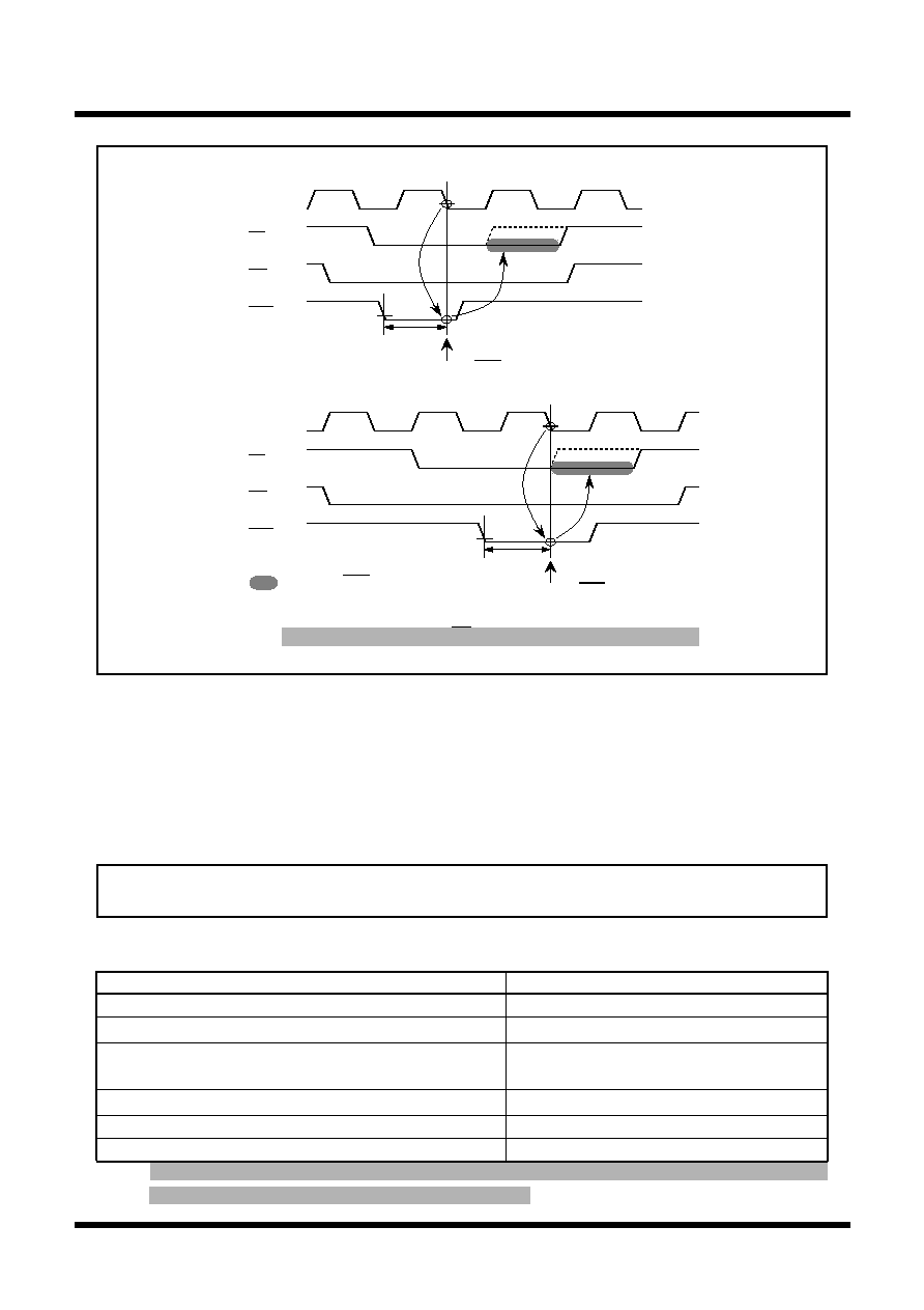
36
Mitsubishi microcomputers
M16C / 62T Group
SINGLE-CHIP 16-BIT CMOS MICROCOMPUTER
Bus Control
_____
________
Figure 1.12.3. Example of RD signal extended by RDY signal
BCLK
tsu
(RDY -
BCLK
)
RDY
RD
tsu
(RDY -
BCLK
)
: Wait using RDY signal
: Wait using software
BCLK
RDY
RD
CS
i
(i=0 to 3)
(Note)
In an instance of separate bus
In an instance of multiplexed bus
Accept timing of RDY signal
Accept timing of RDY signal
Note: In M30623(80-pin package), the CS
i
signal (i = 0 to 3) has no corresponding exte
CS
i
(i=0 to 3)
(Note)
__________
HOLD > DMAC > CPU
(6) Hold signal
The hold signal is used to transfer the bus privileges from the CPU to the external circuits. Inputting "L" to
__________
the HOLD pin places the microcomputer in the hold state at the end of the current bus access. This status
__________
__________
is maintained and "L" is output from the HLDA pin as long as "L" is input to the HOLD pin. Table 1.12.5
shows the microcomputer status in the hold state.
__________
Bus-using priorities are given to HOLD, DMAC, and CPU in order of decreasing precedence.
Figure 1.12.4. Bus-using priorities
Table 1.12.5. Microcomputer status in hold state
Item
Status
Oscillation
ON
___
_____
_______
R/W signal, address bus, data bus, CS, BHE
Floating
Programmable I/O ports
P0, P1, P2, P3, P4, P5
Floating
P6, P7, P8, P9, P10
Maintains status when hold signal is received
__________
HLDA
Output "L"
Internal peripheral circuits
ON (but watchdog timer stops)
ALE signal
Undefined
______
______
Note 1: In M30623(80-pin package), P1, P4
4
to P4
7
(CS0 to CS3) and P7
2
to P7
5
,
P9
1
have no correspond-
ing external pin, but are internally the above conditions.
Mitsubishi microcomputers
M16C / 62T Group
SINGLE-CHIP 16-BIT CMOS MICROCOMPUTER
37
Bus Control
(8) BCLK output
The user can choose the BCLK output by use of bit 7 of processor mode register 0 (0004
16
) (Note).
When set to "1", the output floating.
Note: Before attempting to change the contents of the processor mode register 0, set bit 1 of the protect
register (address 000A
16
) to "1".
(7) External bus status when the internal area is accessed
Table 1.12.6 shows the external bus status when the internal area is accessed.
Table 1.12.6. External bus status when the internal area is accessed
Item
SFR accessed
Internal ROM/RAM accessed
Address bus
Address output
Maintain status before accessed
address of external area
Data bus
When read
Floating
Floating
When write
Output data
Undefined
RD, WR, WRL, WRH
RD, WR, WRL, WRH output
Output "H"
BHE
BHE output
Maintain status before accessed
status of external area
CS
Output "H"
Output "H"
ALE
Output "L"
Output "L"
_____
Note 1: In M30623(80-pin package), CS signals have no corresponding external pin.
38
Mitsubishi microcomputers
M16C / 62T Group
SINGLE-CHIP 16-BIT CMOS MICROCOMPUTER
Bus Control
(9) Software wait
A software wait can be inserted by setting the wait bit (bit 7) of the processor mode register 1 (address
0005
16
) (Note) and bits 4 to 7 of the chip select control register (address 0008
16
).
A software wait is inserted in the internal ROM/RAM area and in the external memory area by setting the
wait bit of the processor mode register 1. When set to "0", each bus cycle is executed in one BCLK cycle.
When set to "1", each bus cycle is executed in two or three BCLK cycles. After the microcomputer has been
reset, this bit defaults to "0". When set to "1", a wait is applied to all memory areas (two or three BCLK
cycles), regardless of the contents of bits 4 to 7 of the chip select control register. Set this bit after referring
to the recommended operating conditions (main clock input oscillation frequency) of the electric character-
istics. However, when the user is using the RDY signal, the relevant bit in the chip select control register's
bits 4 to 7 must be set to "0".
When the wait bit of the processor mode register 1 is "0", software waits can be set independently for
each of the 4 areas selected using the chip select signal. Bits 4 to 7 of the chip select control register
_______
_______
correspond to chip selects CS0 to CS3. When one of these bits is set to "1", the bus cycle is executed in
one BCLK cycle. When set to "0", the bus cycle is executed in two or three BCLK cycles. These bits
default to "0" after the microcomputer has been reset.
The SFR area is always accessed in two BCLK cycles regardless of the setting of these control bits. Also,
insert a software wait if using the multiplex bus to access the external memory area.
Table 1.12.7 shows the software wait and bus cycles. Figure 1.12.5 shows example bus timing when
using software waits.
Note 1: Before attempting to change the contents of the processor mode register 1, set bit 1 of the protect
register (address 000A
16
) to "1".
Note 2: In M30623(80-pin package), the chip select signals have no corresponding external pin.
Table 1.12.7. Software waits and bus cycles
Area
Bus status
Wait bit
Bits 4 to 7 of chip select
control register
Bus cycle
Invalid
1
2 BCLK cycles
External
memory
area
Separate bus
0
1
1 BCLK cycle
Separate bus
0
0
2 BCLK cycles
Separate bus
1
0 (Note)
2 BCLK cycles
Multiplex bus
0
0
3 BCLK cycles
Multiplex bus
1
3 BCLK cycles
0 (Note)
SFR
Internal
ROM/RAM
0
Invalid
1 BCLK cycle
Invalid
Invalid
2 BCLK cycles
Note: When using the RDY signal, always set to "0".
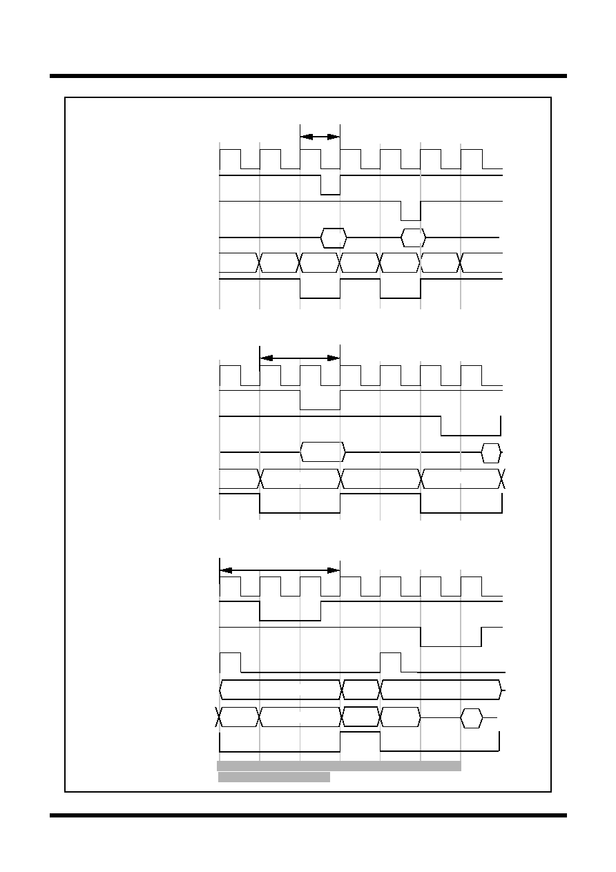
Mitsubishi microcomputers
M16C / 62T Group
SINGLE-CHIP 16-BIT CMOS MICROCOMPUTER
39
Bus Control
Figure 1.12.5. Typical bus timings using software wait
Output
Input
Address
Address
Bus cycle
< Separate bus (with wait) >
BCLK
Read signal
Write signal
Data bus
Address bus
Chip select
BCLK
Read signal
Address bus/
Data bus
Chip select
Address
Address
Address bus
Data output
Address
Address
Input
ALE
Bus cycle
< Multiplexed bus >
Write signal
BCLK
Read signal
Write signal
Address bus
Address
Address
Bus cycle
< Separate bus (no wait) >
Output
Data bus
Chip select
Input
Note 1: In M30623(80-pin package), the chip select signals have no
corresponding external pin.
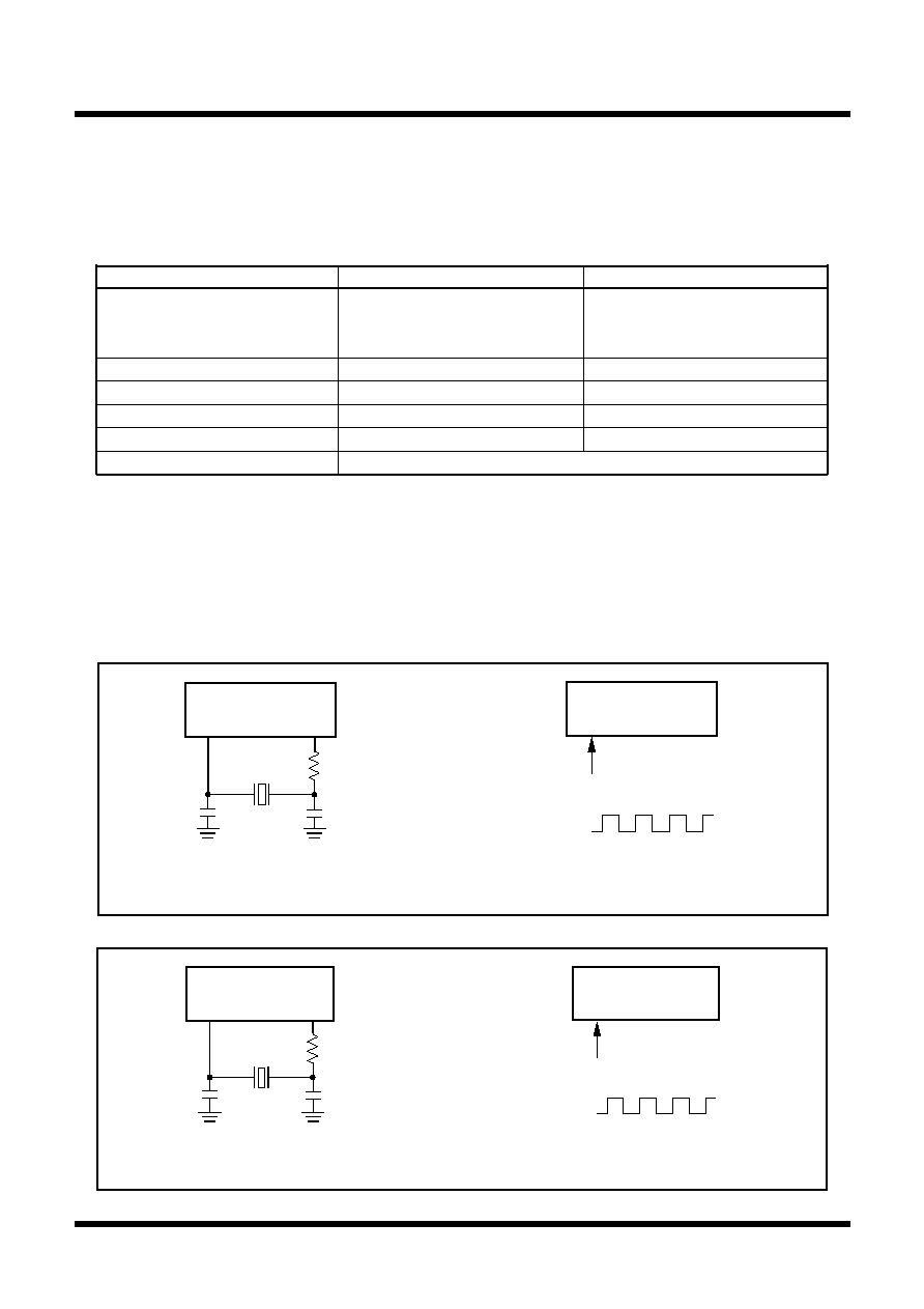
40
Tentative Specifications REV.A
Mitsubishi microcomputers
M16C / 62T Group
SINGLE-CHIP 16-BIT CMOS MICROCOMPUTER
S
pecifications in this manual are tentative and subject to change.
Under
development
Clock Generating Circuit
Figure 1.13.2. Examples of sub clock
Table 1.13.1. Main clock and sub clock generating circuits
Clock Generating Circuit
The clock generating circuit contains two oscillator circuits that supply the operating clock sources to the
CPU and internal peripheral units.
Example of oscillator circuit
Figure 1.13.1 shows some examples of the main clock circuit, one using an oscillator connected to the
circuit, and the other one using an externally derived clock for input. Figure 1.13.2 shows some examples
of sub clock circuits, one using an oscillator connected to the circuit, and the other one using an externally
derived clock for input. Circuit constants in Figures 1.13.1 and 1.13.2 vary with each oscillator used. Use
the values recommended by the manufacturer of your oscillator.
Figure 1.13.1. Examples of main clock
Main clock generating circuit
Sub clock generating circuit
Use of clock
· CPU's operating clock source
· CPU's operating clock source
· Internal peripheral units'
· Timer A/B's count clock
operating clock source
source
Usable oscillator
Ceramic or crystal oscillator
Crystal oscillator
Pins to connect oscillator
X
IN
, X
OUT
X
CIN
, X
COUT
Oscillation stop/restart function
Available
Available
Oscillator status immediately after reset
Oscillating
Stopped
Other
Externally derived clock can be input
Microcomputer
(Built-in feedback resistor)
X
IN
X
OUT
Externally derived clock
Open
Vcc
Vss
Microcomputer
(Built-in feedback resistor)
X
IN
X
OUT
R
d
C
IN
C
OUT
(Note)
Note: Insert a damping resistor if required. The resistance will vary depending on the oscillator and the oscillation drive
capacity setting. Use the value recommended by the maker of the oscillator.
When the oscillation drive capacity is set to low, check that oscillation is stable.
Microcomputer
(Built-in feedback resistor)
X
CIN
X
COUT
Externally derived clock
Open
Vcc
Vss
Note: Insert a damping resistor if required. The resistance will vary depending on the oscillator and the oscillation drive
capacity setting. Use the value recommended by the maker of the oscillator.
When the oscillation drive capacity is set to low, check that oscillation is stable.
Microcomputer
(Built-in feedback resistor)
X
CIN
X
COUT
(Note)
C
CIN
C
COUT
R
Cd
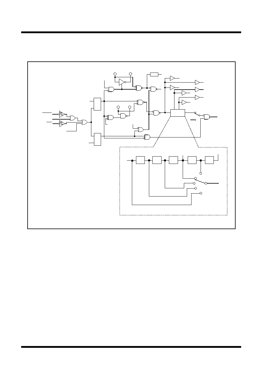
41
Tentative Specifications REV.A
Mitsubishi microcomputers
M16C / 62T Group
SINGLE-CHIP 16-BIT CMOS MICROCOMPUTER
S
pecifications in this manual are tentative and subject to change.
Under
development
Clock Generating Circuit
Clock Control
Figure 1.13.3 shows the block diagram of the clock generating circuit.
Sub clock
CM04
f
C32
CM0i : Bit i at address 0006
16
CM1i : Bit i at address 0007
16
WDCi : Bit i at address 000F
16
X
CIN
CM10 "1"
Write signal
1/32
X
COUT
Q
S
R
WAIT instruction
X
OUT
Main clock
CM05
f
C
CM02
f
1
Q
S
R
NMI
Interrupt request
level judgment
output
RESET
Software reset
f
C
CM07=0
CM07=1
f
AD
Divider
a
d
1/2
1/2
1/2
1/2
CM06=0
CM17,CM16=00
CM06=0
CM17,CM16=01
CM06=0
CM17,CM16=10
CM06=1
CM06=0
CM17,CM16=11
d
a
Details of divider
X
IN
f
8
f
32
c
b
b
1/2
c
f
32
SIO2
f
8
SIO2
f
1
SIO2
BCLK
Figure 1.13.3. Clock generating circuit

42
Tentative Specifications REV.A
Mitsubishi microcomputers
M16C / 62T Group
SINGLE-CHIP 16-BIT CMOS MICROCOMPUTER
S
pecifications in this manual are tentative and subject to change.
Under
development
Clock Generating Circuit
The following paragraphs describes the clocks generated by the clock generating circuit.
(1) Main clock
The main clock is generated by the main clock oscillation circuit. After a reset, the clock is divided by 8 to
the BCLK. The clock can be stopped using the main clock stop bit (bit 5 at address 0006
16
). Stopping the
clock reduces the power dissipation.
After the oscillation of the main clock oscillation circuit has stabilized, the drive capacity of the X
OUT
pin
can be reduced using the X
IN
-X
OUT
drive capacity select bit (bit 5 at address 0007
16
). Reducing the drive
capacity of the X
OUT
pin reduces the power dissipation. This bit defaults to "1" when shifting to stop mode
and after a reset.
(2) Sub clock
The sub clock is generated by the sub clock oscillation circuit. No sub clock is generated after a reset.
After oscillation is started using the port Xc select bit (bit 4 at address 0006
16
), the sub clock can be
selected as the BCLK by using the system clock select bit (bit 7 at address 0006
16
). However, be sure
that the sub clock oscillation has fully stabilized before switching.
After the oscillation of the sub clock oscillation circuit has stabilized, the drive capacity of the X
COUT
pin
can be reduced using the X
CIN
-X
COUT
drive capacity select bit (bit 3 at address 0006
16
). Reducing the
drive capacity of the X
COUT
pin reduces the power dissipation. This bit changes to "1" when shifting to
stop mode and at a reset.
(3) BCLK
The BCLK is the clock that drives the CPU, and is either the main clock or fc or is derived by dividing the
main clock by 2, 4, 8, or 16. The BCLK is derived by dividing the main clock by 8 after a reset.
When shifting to stop mode, the main clock division select bit (bit 6 at 0006
16
) is set to "1".
(4) Peripheral function clock
· f
1
, f
8
, f
32,
f
1SIO2,
f
8SIO2,
f
32SIO2
The clock for the peripheral devices is derived from the main clock or by dividing it by 8 or 32. The
peripheral function clock is stopped by stopping the main clock or by setting the WAIT peripheral function
clock stop bit (bit 2 at 0006
16
) to "1" and then executing a WAIT instruction.
· f
AD
This clock has the same frequency as the main clock and is used for A-D conversion.
(5) f
C32
This clock is derived by dividing the sub clock by 32. It is used for the timer A and timer B counts.
(6) f
C
This clock has the same frequency as the sub clock. It is used for the BCLK and for the watchdog timer.
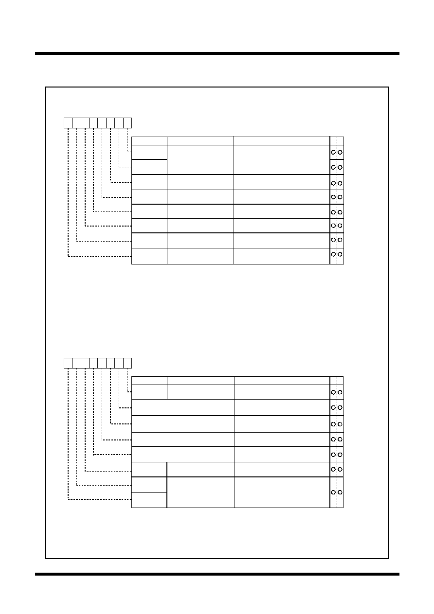
43
Tentative Specifications REV.A
Mitsubishi microcomputers
M16C / 62T Group
SINGLE-CHIP 16-BIT CMOS MICROCOMPUTER
S
pecifications in this manual are tentative and subject to change.
Under
development
Clock Generating Circuit
Figure 1.13.4 shows the system clock control registers 0 and 1.
Figure 1.13.4. Clock control registers 0 and 1
System clock control register 0 (Note 1)
Symbol
Address
When reset
CM0
0006
16
48
16
Bit name
Function
Bit symbol
b7
b6
b5
b4
b3
b2
b1
b0
0 0 : I/O port P5
7
0 1 : f
C
output
1 0 : f
8
output
1 1 : f
32
output
b1 b0
CM07
CM05
CM04
CM03
CM01
CM02
CM00
CM06
Clock output function
select bit
WAIT peripheral function
clock stop bit
0 : Do not stop f
1
, f
8
, f
32
in wait mode
1 : Stop f
1
, f
8
, f
32
in wait mode
X
CIN
-X
COUT
drive capacity
select bit (Note 2)
0 : LOW
1 : HIGH
Port X
C
select bit
0 : I/O port
1 : X
CIN
-X
COUT
generation
Main clock (X
IN
-X
OUT
)
stop bit (Note 4) (Note 5)
0 : On
1 : Off
Main clock division select
bit 0 (Note 2)
0 : CM16 and CM17 valid
1 : Division by 8 mode
System clock select bit
(Note 6)
0 : X
IN
, X
OUT
1 : X
CIN
, X
COUT
Note 1: Set bit 0 of the protect register (address 000A
16
) to "1" before writing to this register.
Note 2: Changes to "1" when shiffing to stop mode.
Note 3: When entering power saving mode, main clock stops using this bit. When returning from stop
mode and operating with X
IN
, set this bit to "0". When main clock oscillation is operating by
itself, set system clock select bit (CM07) to "1" before setting this bit to "1".
Note 4: When inputting external clock, only clock oscillation buffer is stopped and clock input is acceptable.
Note 5: If this bit is set to "1", X
OUT
turns "H". The built-in feedback resistor remains ON, so X
IN
turns pulled
up to X
OUT
("H") via the feedback resistor.
Note 6: Set port Xc select bit (CM04) to "1" before writing to this bit. The both bits can not be written at
the same time.
System clock control register 1 (Note 1)
Symbol
Address
When reset
CM1
0007
16
20
16
Bit name
Function
Bit symbol
b7
b6
b5
b4
b3
b2
b1
b0
CM10
All clock stop control bit
(Note4)
0 : Clock on
1 : All clocks off (stop mode)
Note 1: Set bit 0 of the protect register (address 000A
16
) to
"1" before writing to this register.
Note 2: Changes to
"1" when shiffing to stop mode.
Note 3: Can be selected when bit 6 of the system clock control register 0 (address 0006
16
) is
"0".
If
"1", division mode is fixed at 8.
Note 4: If this bit is set to "1", X
OUT
turns "H", and the built-in feedback resistor turns null.
CM15
X
IN
-X
OUT
drive capacity
select bit (Note 2)
0 : LOW
1 : HIGH
W
R
W
R
CM16
CM17
Reserved bit
Always set to
"0"
Reserved bit
Always set to
"0"
Main clock division
select bit 1 (Note 3)
0 0 : No division mode
0 1 : Division by 2 mode
1 0 : Division by 4 mode
1 1 : Division by 16 mode
b7 b6
0
0
Reserved bit
Always set to
"0"
Reserved bit
Always set to
"0"
0
0
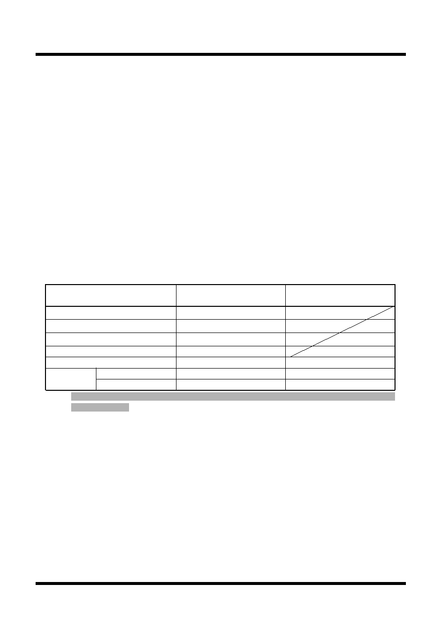
44
Tentative Specifications REV.A
Mitsubishi microcomputers
M16C / 62T Group
SINGLE-CHIP 16-BIT CMOS MICROCOMPUTER
S
pecifications in this manual are tentative and subject to change.
Under
development
Clock Generating Circuit
Clock Output
In single-chip mode, the clock output function select bits (bits 0 and 1 at address 0006
16
) enable f
8
, f
32
, or
fc to be output from the P5
7
/CLK
OUT
pin. When the WAIT peripheral function clock stop bit (bit 2 at address
0006
16
) is set to "1", the output of f
8
and f
32
stops when a WAIT instruction is executed.
Stop Mode
Writing "1" to the all-clock stop control bit (bit 0 at address 0007
16
) stops all oscillation and the microcom-
puter enters stop mode. In stop mode, the content of the internal RAM is retained provided that V
CC
re-
mains above 2V.
Because the oscillation , BCLK, f
1
to f
32
, f
1SIO2
to f
32SIO2
, f
C
, f
C32
, and f
AD
stops in stop mode, peripheral
functions such as the A-D converter and watchdog timer do not function. However, timer A and timer B
operate provided that the event counter mode is set to an external pulse, and UARTi(i = 0 to 2) functions
provided an external clock is selected. Table 1.13.2 shows the status of the ports in stop mode.
Stop mode is cancelled by a hardware reset or interrupt. If an interrupt is to be used to cancel stop mode,
that interrupt must first have been enabled.
When shifting to stop mode, the main clock division select bit 0 (bit 6 at 0006
16
) is set to "1".
Note 1:
______
______
In M30623(80-pin package), CS0 to CS3 have no corresponding external pin, but are internally the
above conditions.
Table 1.13.2. Port status during stop mode
Pin
Memory expansion mode
Single-chip mode
Microprocessor mode
_______
_______
Address bus, data bus, CS0 to CS3
Retains status before stop mode
_____
______
________
________
_________
RD, WR, BHE, WRL, WRH
"H"
__________
HLDA, BCLK
"H"
ALE
"H"
Port
Retains status before stop mode
Retains status before stop mode
CLK
OUT
When fc selected
Valid only in single-chip mode
"H"
When f
8
, f
32
selected
Valid only in single-chip mode
Retains status before stop mode
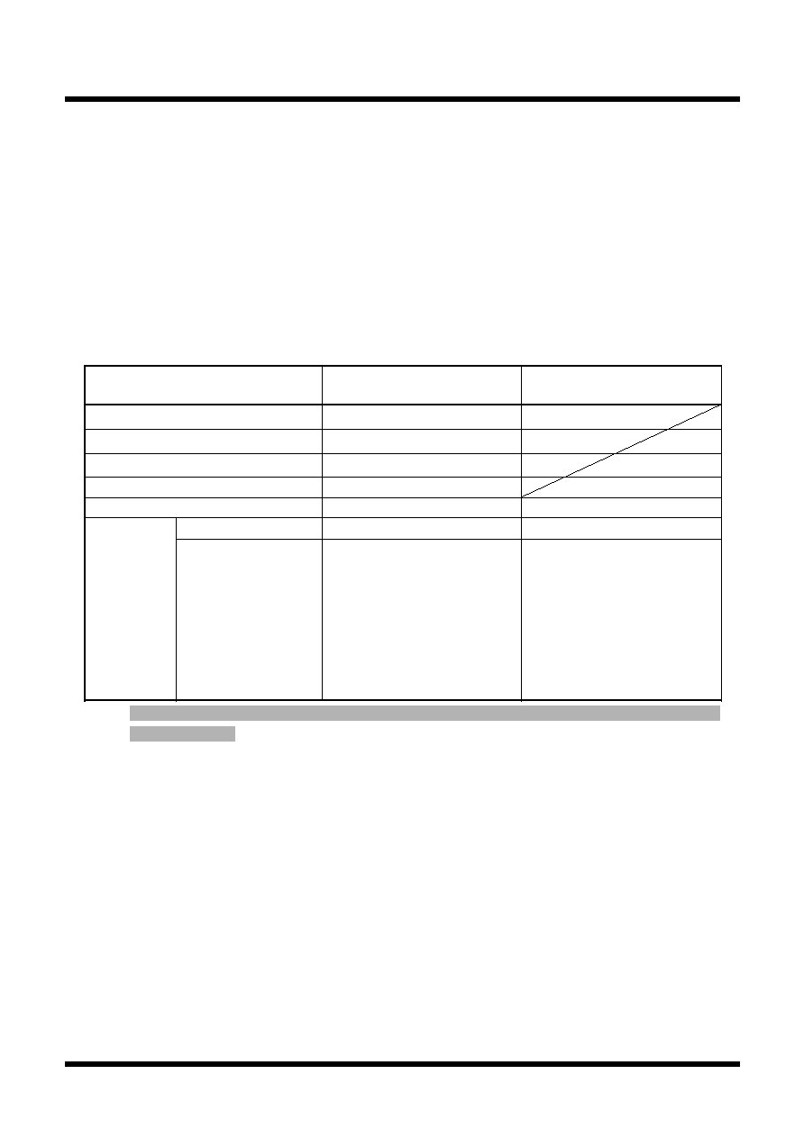
45
Tentative Specifications REV.A
Mitsubishi microcomputers
M16C / 62T Group
SINGLE-CHIP 16-BIT CMOS MICROCOMPUTER
S
pecifications in this manual are tentative and subject to change.
Under
development
Wait Mode
When a WAIT instruction is executed, the BCLK stops and the microcomputer enters the wait mode. In this
mode, oscillation continues but the BCLK and watchdog timer stop. Writing "1" to the WAIT peripheral
function clock stop bit and executing a WAIT instruction stops the clock being supplied to the internal
peripheral functions, allowing power dissipation to be reduced. Table 1.13.3 shows the status of the ports in
wait mode.
Wait mode is cancelled by a hardware reset or interrupt. If an interrupt is used to cancel wait mode, the
microcomputer restarts using as BCLK, the clock that had been selected when the WAIT instruction was
executed.
Wait Mode
Table 1.13.3. Port status during wait mode
Pin
Memory expansion mode
Single-chip mode
Microprocessor mode
_______
_______
Address bus, data bus, CS0 to CS3
Retains status before wait mode
_____
______
________
________
_________
RD, WR, BHE, WRL, WRH
"H"
__________
HLDA,BCLK
"H"
ALE
"H"
Port
Retains status before wait mode
Retains status before wait mode
CLK
OUT
When f
C
selected
Valid only in single-chip mode
Does not stop
When f
8
, f
32
selected
Valid only in single-chip mode
Does not stop when the WAIT
peripheral function clock stop
bit is "0".
When the WAIT peripheral
function clock stop bit is "1", the
status immediately prior to en-
tering wait mode is main-
tained.
Note 1:
______
______
In M30623(80-pin package), CS0 to CS3 have no corresponding external pin, but are internally the
above conditions.
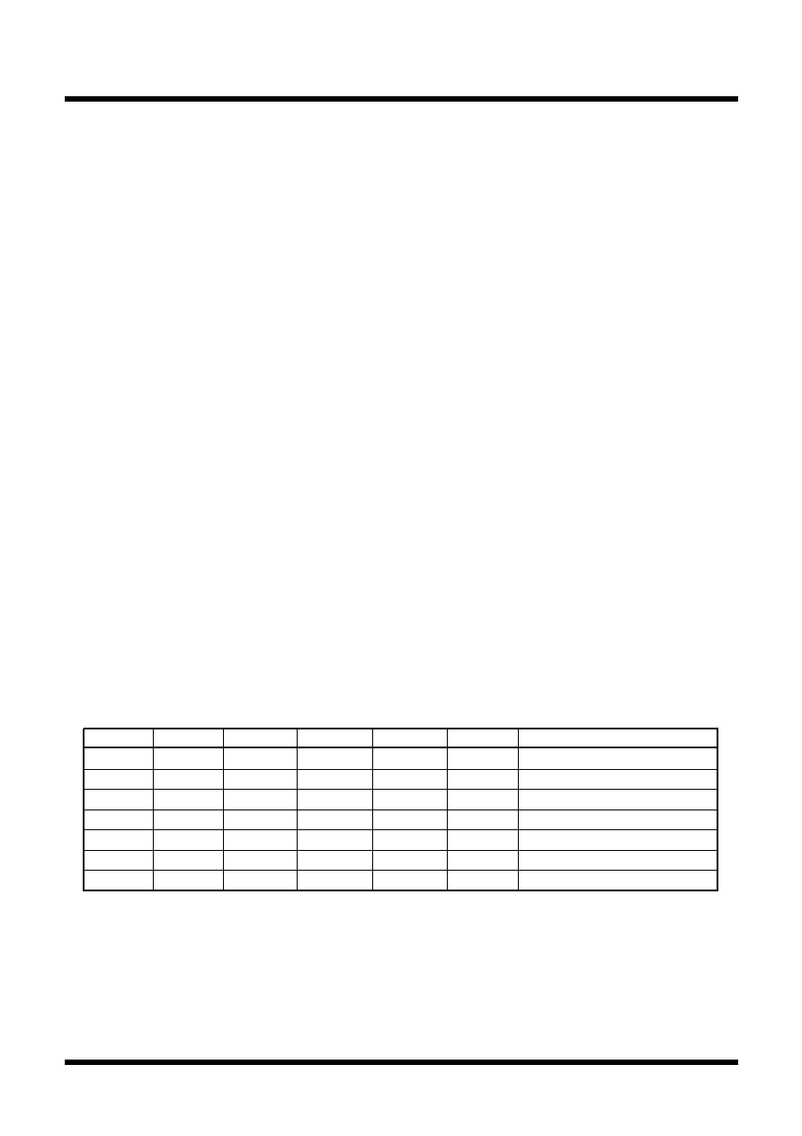
46
Tentative Specifications REV.A
Mitsubishi microcomputers
M16C / 62T Group
SINGLE-CHIP 16-BIT CMOS MICROCOMPUTER
S
pecifications in this manual are tentative and subject to change.
Under
development
Status Transition of BCLK
Power dissipation can be reduced and low-voltage operation achieved by changing the count source for
BCLK. Table 1.13.4 shows the operating modes corresponding to the settings of system clock control
registers 0 and 1.
After a reset, operation defaults to division by 8 mode. When shifting to stop mode, the main clock division
select bit 0 (bit 6 at address 0006
16
) is set to "1". The following shows the operational modes of BCLK.
(1) Division by 2 mode
The main clock is divided by 2 to obtain the BCLK.
(2) Division by 4 mode
The main clock is divided by 4 to obtain the BCLK.
(3) Division by 8 mode
The main clock is divided by 8 to obtain the BCLK. Note that oscillation of the main clock must have
stabilized before transferring from this mode to another mode.
(4) Division by 16 mode
The main clock is divided by 16 to obtain the BCLK.
(5) No-division mode
The main clock is used as the BCLK.
(6) Low-speed mode
f
C
is used as the BCLK. Note that oscillation of both the main and sub clocks must have stabilized before
transferring from this mode to another or vice versa. At least 2 to 3 seconds are required after the sub
clock starts. Therefore, the program must be written to wait until this clock has stabilized immediately
after powering up and after stop mode is cancelled.
(7) Low power dissipation mode
f
C
is the BCLK and the main clock is stopped.
Status Transition of BCLK
0
1
0
0
0
Invalid
Division by 2 mode
1
0
0
0
0
Invalid
Division by 4 mode
Invalid
Invalid
0
1
0
Invalid
Division by 8 mode
1
1
0
0
0
Invalid
Division by 16 mode
0
0
0
0
0
Invalid
No-division mode
Invalid
Invalid
1
Invalid
0
1
Low-speed mode
Invalid
Invalid
1
Invalid
1
1
Low power dissipation mode
CM17
CM16
CM07
CM06
CM05
CM04
Operating mode of BCLK
Table 1.13.4. Operating modes dictated by settings of system clock control registers 0 and 1

47
Tentative Specifications REV.A
Mitsubishi microcomputers
M16C / 62T Group
SINGLE-CHIP 16-BIT CMOS MICROCOMPUTER
S
pecifications in this manual are tentative and subject to change.
Under
development
Power control
The following is a description of the three available power control modes:
Modes
Power control is available in three modes.
(a) Normal operation mode
· High-speed mode
Divide-by-1 frequency of the main clock becomes the BCLK. The CPU operates with the internal
clock selected. Each peripheral function operates according to its assigned clock.
· Medium-speed mode
Divide-by-2, divide-by-4, divide-by-8, or divide-by-16 frequency of the main clock becomes the
BCLK. The CPU operates according to the internal clock selected. Each peripheral function oper-
ates according to its assigned clock.
· Low-speed mode
f
C
becomes the BCLK. The CPU operates according to the fc clock. The fc clock is supplied by the
secondary clock. Each peripheral function operates according to its assigned clock.
· Low power consumption mode
The main clock operating in low-speed mode is stopped. The CPU operates according to the f
C
clock. The fc clock is supplied by the secondary clock. The only peripheral functions that operate
are those with the sub-clock selected as the count source.
(b) Wait mode
The CPU operation is stopped. The oscillators do not stop.
(c) Stop mode
All oscillators stop. The CPU and all built-in peripheral functions stop. This mode, among the three
modes listed here, is the most effective in decreasing power consumption.
Figure 1.13.5 is the state transition diagram of the above modes.
Power control
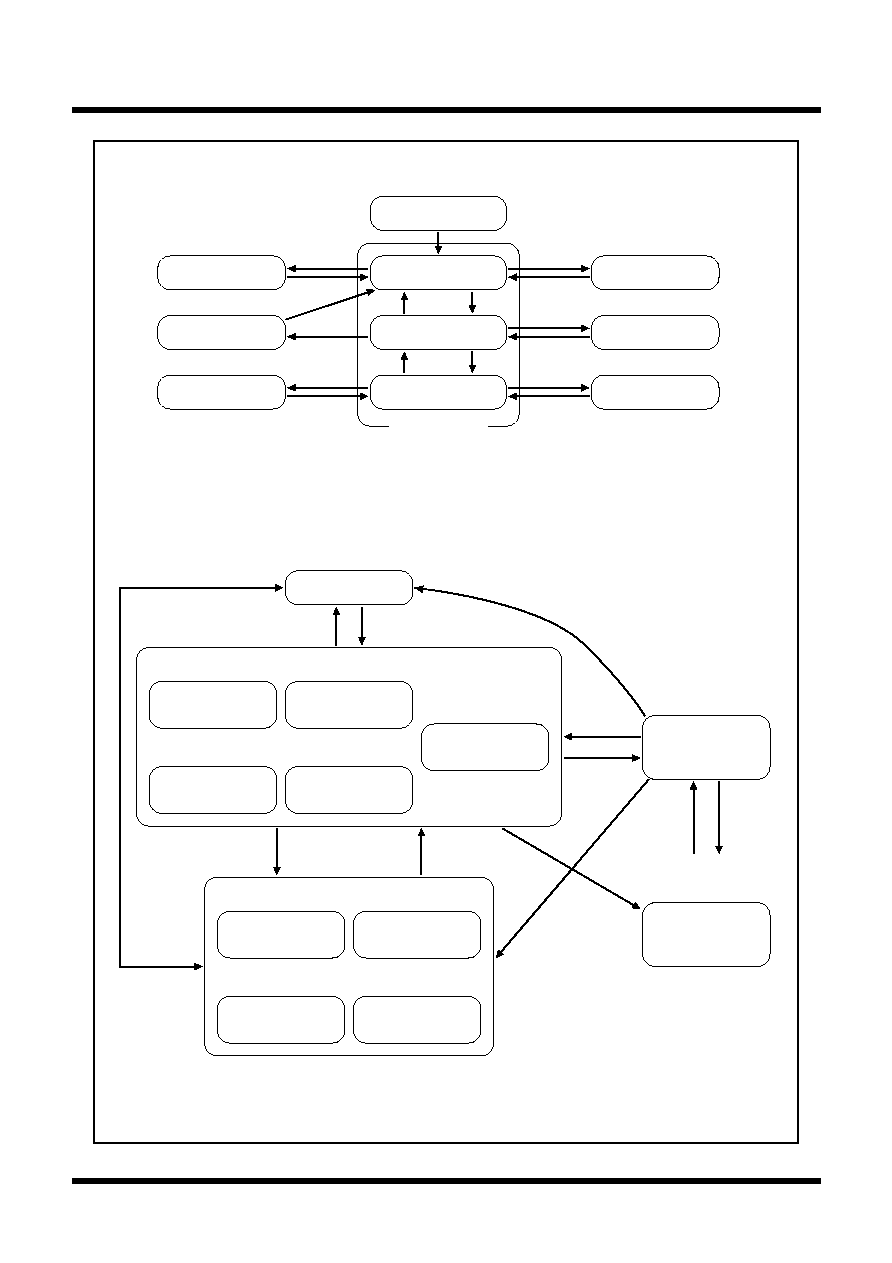
48
Tentative Specifications REV.A
Mitsubishi microcomputers
M16C / 62T Group
SINGLE-CHIP 16-BIT CMOS MICROCOMPUTER
S
pecifications in this manual are tentative and subject to change.
Under
development
Figure 1.13.5. State transition diagram of Power control mode
Transition of stop mode, wait mode
Transition of normal mode
Reset
Medium-speed mode
(divided-by-8 mode)
Interrupt
CM10 = "1"
All oscillators stopped
CPU operation stopped
Medium-speed mode
(divided-by-8 mode)
BCLK : f(X
IN
)/8
CM07 = "0" CM06 = "1"
Low-speed mode
High-speed mode
Main clock is oscillating
Sub clock is stopped
Main clock is oscillating
Sub clock is stopped
Main clock is stopped
Sub clock is oscillating
Main clock is oscillating
Sub clock is oscillating
Low power dissipation mode
High-speed/medium-
speed mode
Low-speed/low power
dissipation mode
Normal mode
Stop mode
Stop mode
Stop mode
All oscillators stopped
All oscillators stopped
Wait mode
Wait mode
Wait mode
CPU operation stopped
CPU operation stopped
Interrupt
WAIT
instruction
Interrupt
WAIT
instruction
Interrupt
WAIT
instruction
CM10 = "1"
Interrupt
Interrupt
CM10 = "1"
BCLK : f(X
IN
)/2
CM07 = "0" CM06 = "0"
CM17 = "0" CM16 = "1"
Medium-speed mode
(divided-by-2 mode)
BCLK : f(X
IN
)/16
CM07 = "0" CM06 = "0"
CM17 = "1" CM16 = "1"
Medium-speed mode
(divided-by-16 mode)
BCLK : f(X
IN
)/4
CM07 = "0" CM06 = "0"
CM17 = "1" CM16 = "0"
Medium-speed mode
(divided-by-4 mode)
BCLK : f(X
IN
)
CM07 = "0" CM06 = "0"
CM17 = "0" CM16 = "0"
BCLK : f(X
IN
)/8
Medium-speed mode
(divided-by-8 mode)
CM07 = "0"
CM06 = "1"
High-speed mode
BCLK : f(X
IN
)/2
CM07 = "0" CM06 = "0"
CM17 = "0" CM16 = "1"
Medium-speed mode
(divided-by-2 mode)
BCLK : f(X
IN
)/16
CM07 = "0" CM06 = "0"
CM17 = "1" CM16 = "1"
Medium-speed mode
(divided-by-16 mode)
BCLK : f(X
IN
)/4
CM07 = "0" CM06 = "0"
CM17 = "1" CM16 = "0"
Medium-speed mode
(divided-by-4 mode)
BCLK : f(X
IN
)
CM07 = "0" CM06 = "0"
CM17 = "0" CM16 = "0"
BCLK : f(X
CIN
)
CM07 = "1"
BCLK : f(X
CIN
)
CM07 = "1"
Main clock is oscillating
Sub clock is oscillating
CM07 = "0"
(Note 1, 3)
CM07 = "0" (Note 1)
CM06 = "1"
CM04 = "0"
CM07 = "1"
(Note 2)
CM07 = "0" (Note 1)
CM06 = "0" (Note 3)
CM04 = "1"
CM07 = "1" (Note 2)
CM05 = "1"
CM05 = "0"
CM05 = "1"
CM04 = "0"
CM04 = "1"
CM06 = "0"
(Notes 1,3)
CM06 = "1"
CM04 = "0"
CM04 = "1"
(Notes 1, 3)
Note 1: Switch clock after oscillation of main clock is sufficiently stable.
Note 2: Switch clock after oscillation of sub clock is sufficiently stable.
Note 3: Change CM06 after changing CM17 and CM16.
Note 4: Transit in accordance with arrow.
(Refer to the following for the transition of normal mode.)
Power control
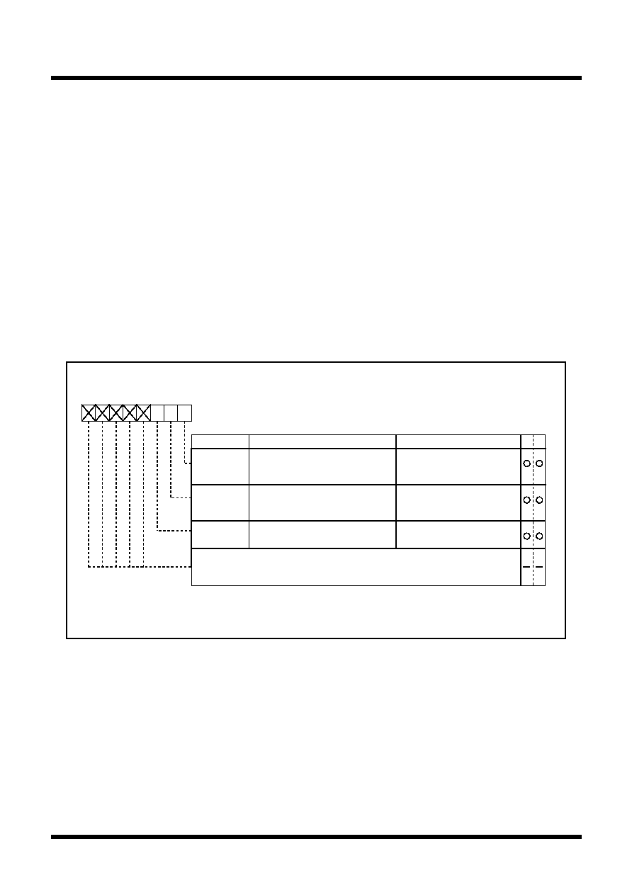
49
Tentative Specifications REV.A
Mitsubishi microcomputers
M16C / 62T Group
SINGLE-CHIP 16-BIT CMOS MICROCOMPUTER
S
pecifications in this manual are tentative and subject to change.
Under
development
Protection
The protection function is provided so that the values in important registers cannot be changed in the event
that the program runs out of control. Figure 1.13.6 shows the protect register. The values in the processor
mode register 0 (address 0004
16
), processor mode register 1 (address 0005
16
), system clock control reg-
ister 0 (address 0006
16
), system clock control register 1 (address 0007
16
), port P9 direction register (ad-
dress 03F3
16
) , SI/O3 control register (address 0362
16
) and SI/O4 control register (address 0366
16
) can
only be changed when the respective bit in the protect register is set to "1". Therefore, important outputs
can be allocated to port P9.
If, after "1" (write-enabled) has been written to the port P9 direction register and SI/Oi control register
(i=3,4) write-enable bit (bit 2 at address 000A
16
), a value is written to any address, the bit automatically
reverts to "0" (write-inhibited). However, the system clock control registers 0 and 1 write-enable bit (bit 0 at
000A
16
) and processor mode register 0 and 1 write-enable bit (bit 1 at 000A
16
) do not automatically return
to "0" after a value has been written to an address. The program must therefore be written to return these
bits to "0".
Protect register
Symbol
Address
When reset
PRCR
000A
16
XXXXX000
2
Bit name
Bit symbol
b7
b6
b5
b4
b3
b2
b1
b0
0 : Write-inhibited
1 : Write-enabled
PRC1
PRC0
PRC2
Enables writing to processor mode
registers 0 and 1 (addresses 0004
16
and 0005
16
)
Function
0 : Write-inhibited
1 : Write-enabled
Enables writing to system clock
control registers 0 and 1 (addresses
0006
16
and 0007
16
)
Enables writing to port P9 direction
register (address 03F3
16
) (Note 1
)
0 : Write-inhibited
1 : Write-enabled
W
R
Nothing is assigned.
In an attempt to write to these bits, write "0". The value, if read, turns out to be
indeterminate.
Note 1: Writing a value to an address after "1" is written to this bit returns the bit
to "0" . Other bits do not automatically return to "0" and they must therefore
be reset by the program.
Figure 1.13.6. Protect register
Protection

50
Tentative Specifications REV.A
Mitsubishi microcomputers
M16C / 62T Group
SINGLE-CHIP 16-BIT CMOS MICROCOMPUTER
S
pecifications in this manual are tentative and subject to change.
Under
development
Interrupt
· Maskable interrupt :
An interrupt which can be enabled (disabled) by the interrupt enable flag
(I flag) or whose interrupt priority can be changed by priority level.
· Non-maskable interrupt : An interrupt which cannot be enabled (disabled) by the interrupt enable flag
(I flag) or whose interrupt priority cannot be changed by priority level.
Figure 1.14.1. Classification of interrupts
Interrupt
Software
Hardware
Special
Peripheral I/O (Note)
Undefined instruction (UND instruction)
Overflow (INTO instruction)
BRK instruction
INT instruction
Reset
_______
NMI
________
DBC
Watchdog timer
Single step
Address matched
Note: Peripheral I/O interrupts are generated by the peripheral functions built into the microcomputer system.
Overview of Interrupt
Type of Interrupts
Figure 1.14.1 lists the types of interrupts.

51
Tentative Specifications REV.A
Mitsubishi microcomputers
M16C / 62T Group
SINGLE-CHIP 16-BIT CMOS MICROCOMPUTER
S
pecifications in this manual are tentative and subject to change.
Under
development
Interrupt
Software Interrupts
A software interrupt occurs when executing certain instructions. Software interrupts are non-maskable
interrupts.
· Undefined instruction interrupt
An undefined instruction interrupt occurs when executing the UND instruction.
· Overflow interrupt
An overflow interrupt occurs when executing the INTO instruction with the overflow flag (O flag) set to
"1". The following are instructions whose O flag changes by arithmetic:
ABS, ADC, ADCF, ADD, CMP, DIV, DIVU, DIVX, NEG, RMPA, SBB, SHA, SUB
· BRK interrupt
A BRK interrupt occurs when executing the BRK instruction.
· INT interrupt
An INT interrupt occurs when assiging one of software interrupt numbers 0 through 63 and executing
the INT instruction. Software interrupt numbers 0 through 31 are assigned to peripheral I/O interrupts,
so executing the INT instruction allows executing the same interrupt routine that a peripheral I/O
interrupt does.
The stack pointer (SP) used for the INT interrupt is dependent on which software interrupt number is
involved.
So far as software interrupt numbers 0 through 31 are concerned, the microcomputer saves the stack
pointer assignment flag (U flag) when it accepts an interrupt request. If change the U flag to "0" and
select the interrupt stack pointer (ISP), and then execute an interrupt sequence. When returning from
the interrupt routine, the U flag is returned to the state it was before the acceptance of interrupt re-
quest. So far as software numbers 32 through 63 are concerned, the stack pointer does not make a
shift.

52
Tentative Specifications REV.A
Mitsubishi microcomputers
M16C / 62T Group
SINGLE-CHIP 16-BIT CMOS MICROCOMPUTER
S
pecifications in this manual are tentative and subject to change.
Under
development
Interrupt
Hardware Interrupts
Hardware interrupts are classified into two types -- special interrupts and peripheral I/O interrupts.
(1) Special interrupts
Special interrupts are non-maskable interrupts.
· Reset
____________
Reset occurs if an "L" is input to the RESET pin.
_______
· NMI interrupt
_______
_______
An NMI interrupt occurs if an "L" is input to the NMI pin.
________
· DBC interrupt
This interrupt is exclusively for the debugger, do not use it in other circumstances.
· Watchdog timer interrupt
Generated by the watchdog timer.
· Single-step interrupt
This interrupt is exclusively for the debugger, do not use it in other circumstances. With the debug
flag (D flag) set to "1", a single-step interrupt occurs after one instruction is executed.
· Address match interrupt
An address match interrupt occurs immediately before the instruction held in the address indicated by
the address match interrupt register is executed with the address match interrupt enable bit set to "1".
If an address other than the first address of the instruction in the address match interrupt register is set,
no address match interrupt occurs. For address match interrupt, see 2.11 Address match Interrupt.
(2) Peripheral I/O interrupts
A peripheral I/O interrupt is generated by one of built-in peripheral functions. Built-in peripheral func-
tions are dependent on classes of products, so the interrupt factors too are dependent on classes of
products. The interrupt vector table is the same as the one for software interrupt numbers 0 through
31 the INT instruction uses. Peripheral I/O interrupts are maskable interrupts.
· Bus collision detection interrupt
This is an interrupt that the serial I/O bus collision detection generates.
· DMA0 interrupt, DMA1 interrupt
These are interrupts that DMA generates.
· Key-input interrupt
___
A key-input interrupt occurs if an "L" is input to the KI pin.
· A-D conversion interrupt
This is an interrupt that the A-D converter generates.
· UART0, UART1, UART2/NACK, SI/O3 and SI/O4 transmission interrupt
These are interrupts that the serial I/O transmission generates.
· UART0, UART1, UART2/ACK, SI/O3 and SI/O4 reception interrupt
These are interrupts that the serial I/O reception generates.
· Timer A0 interrupt through timer A4 interrupt
These are interrupts that timer A generates
· Timer B0 interrupt through timer B5 interrupt
These are interrupts that timer B generates.
________
________
· INT0 interrupt through INT5 interrupt
______
______
An INT interrupt occurs if either a rising edge or a falling edge or a both edge is input to the INT pin.
Note 1:
_______
_______
In M30623 (80-pin package), can not use INT
3
to INT
5
as the interrupt factors, because
_______
_______
P1
5
/D
13
/INT
3
to P1
7
/D
15
/INT
5
have no corresponding external pin.
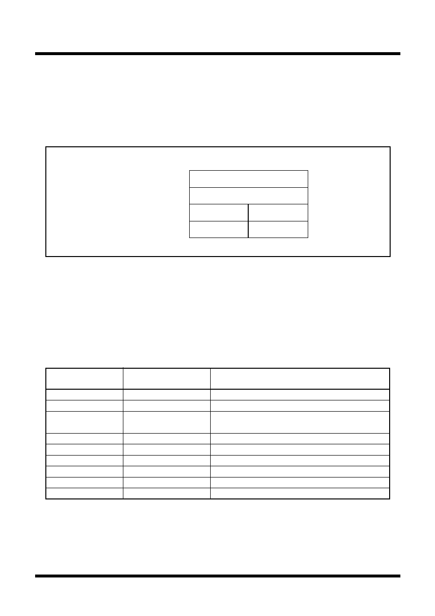
53
Tentative Specifications REV.A
Mitsubishi microcomputers
M16C / 62T Group
SINGLE-CHIP 16-BIT CMOS MICROCOMPUTER
S
pecifications in this manual are tentative and subject to change.
Under
development
Interrupt
Interrupt source
Vector table addresses
Remarks
Address (L) to address (H)
Undefined instruction
FFFDC
16
to FFFDF
16
Interrupt on UND instruction
Overflow
FFFE0
16
to FFFE3
16
Interrupt on INTO instruction
BRK instruction
FFFE4
16
to FFFE7
16
If the vector contains FF
16
, program execution starts from
the address shown by the vector in the variable vector table
Address match
FFFE8
16
to FFFEB
16
There is an address-matching interrupt enable bit
Single step (Note)
FFFEC
16
to FFFEF
16
Do not use
Watchdog timer
FFFF0
16
to FFFF3
16
________
DBC (Note)
FFFF4
16
to FFFF7
16
Do not use
NMI
FFFF8
16
to FFFFB
16
_______
External interrupt by input to NMI pin
Reset
FFFFC
16
to FFFFF
16
Note: Interrupts used for debugging purposes only.
Figure 1.14.2. Format for specifying interrupt vector addresses
Mid address
Low address
0 0 0 0
High address
0 0 0 0
0 0 0 0
Vector address + 0
Vector address + 1
Vector address + 2
Vector address + 3
LSB
MSB
Interrupts and Interrupt Vector Tables
If an interrupt request is accepted, a program branches to the interrupt routine set in the interrupt vector
table. Set the first address of the interrupt routine in each vector table. Figure 1.14.2 shows the format for
specifying the address.
Two types of interrupt vector tables are available -- fixed vector table in which addresses are fixed and
variable vector table in which addresses can be varied by the setting.
· Fixed vector tables
The fixed vector table is a table in which addresses are fixed. The vector tables are located in an area
extending from FFFDC
16
to FFFFF
16
. One vector table comprises four bytes. Set the first address of
interrupt routine in each vector table. Table 1.14.1 shows the interrupts assigned to the fixed vector
tables and addresses of vector tables.
Table 1.14.1. Interrupts assigned to the fixed vector tables and addresses of vector tables
54
Tentative Specifications REV.A
Mitsubishi microcomputers
M16C / 62T Group
SINGLE-CHIP 16-BIT CMOS MICROCOMPUTER
S
pecifications in this manual are tentative and subject to change.
Under
development
Interrupt
Table 1.14.2. Interrupts assigned to the variable vector tables and addresses of vector tables
Software interrupt number
Interrupt source
Vector table address
Address (L) to address (H)
Remarks
Cannot be masked I flag
+0 to +3 (Note 1)
BRK instruction
Software interrupt number 0
+44 to +47 (Note 1)
Software interrupt number 11
+48 to +51 (Note 1)
Software interrupt number 12
+52 to +55 (Note 1)
Software interrupt number 13
+56 to +59 (Note 1)
Software interrupt number 14
+68 to +71 (Note 1)
Software interrupt number 17
+72 to +75 (Note 1)
Software interrupt number 18
+76 to +79 (Note 1)
Software interrupt number 19
+80 to +83 (Note 1)
Software interrupt number 20
+84 to +87 (Note 1)
Software interrupt number 21
+88 to +91 (Note 1)
Software interrupt number 22
+92 to +95 (Note 1)
Software interrupt number 23
+96 to +99 (Note 1)
Software interrupt number 24
+100 to +103 (Note 1)
Software interrupt number 2
5
+104 to +107 (Note 1)
Software interrupt number 26
+108 to +111 (Note 1)
Software interrupt number 27
+112 to +115 (Note 1)
Software interrupt number 28
+116 to +119 (Note 1)
Software interrupt number 29
+120 to +123 (Note 1)
Software interrupt number 30
+124 to +127 (Note 1)
Software interrupt number 31
+128 to +131 (Note 1)
Software interrupt number 32
+252 to +255 (Note 1)
Software interrupt number 63
to
Note 1: Address relative to address in interrupt table register (INTB).
Note 2: It is selected by interrupt request cause bit (bit 6, 7 in address 035F16 ).
Note 3: When IIC mode is selected, NACK and ACK interrupts are selected.
Note 4: In M30623 (80-pin package), can not use INT3 to INT5 as the interrupt factor, because P1
5
/D
13
/INT
3
to
P1
7
/D
15
/INT
5
have no corresponding external pin.
Cannot be masked I flag
+40 to +43 (Note 1)
Software interrupt number 10
+60 to +63 (Note 1)
Software interrupt number 15
+64 to +67 (Note 1)
Software interrupt number 16
+20 to +23 (Note 1)
Software interrupt number 5
+24 to +27 (Note 1)
Software interrupt number 6
+28 to +31 (Note 1)
Software interrupt number 7
+32 to +35 (Note 1)
Software interrupt number 8
+16 to +19 (Note 1)
INT3
Software interrupt number 4
+36 to +39 (Note 1)
SI/O3/INT4
Software interrupt number 9
SI/O4/INT5
Timer B3
Timer B4
Timer B5
(Note 2, Note 4)
(Note 2, Note 4)
to
DMA0
DMA1
Key input interrupt
A-D
UART0 transmit
UART0 receive
UART1 transmit
UART1 receive
Timer A0
Timer A1
Timer A2
Timer A3
Timer A4
Timer B0
Timer B1
Timer B2
INT0
INT1
INT2
Software interrupt
Bus collision detection
UART2 transmit/NACK (Note 3)
UART2 receive/ACK (Note 3)
(Note 4)
· Variable vector tables
The addresses in the variable vector table can be modified, according to the user's settings. Indicate
the first address using the interrupt table register (INTB). The 256-byte area subsequent to the ad-
dress the INTB indicates becomes the area for the variable vector tables. One vector table comprises
four bytes. Set the first address of the interrupt routine in each vector table. Table 1.14.2 shows the
interrupts assigned to the variable vector tables and addresses of vector tables.

55
Tentative Specifications REV.A
Mitsubishi microcomputers
M16C / 62T Group
SINGLE-CHIP 16-BIT CMOS MICROCOMPUTER
S
pecifications in this manual are tentative and subject to change.
Under
development
Interrupt
Interrupt Control
Descriptions are given here regarding how to enable or disable maskable interrupts and how to set the
priority to be accepted. What is described here does not apply to non-maskable interrupts.
Enable or disable a maskable interrupt using the interrupt enable flag (I flag), interrupt priority level selec-
tion bit, or processor interrupt priority level (IPL). Whether an interrupt request is present or absent is
indicated by the interrupt request bit. The interrupt request bit and the interrupt priority level selection bit
are located in the interrupt control register of each interrupt. Also, the interrupt enable flag (I flag) and the
IPL are located in the flag register (FLG).
Figure 1.14.3 shows the memory map of the interrupt control registers.
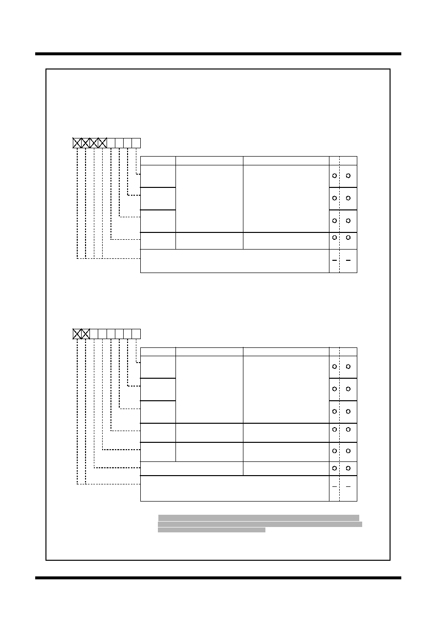
56
Tentative Specifications REV.A
Mitsubishi microcomputers
M16C / 62T Group
SINGLE-CHIP 16-BIT CMOS MICROCOMPUTER
S
pecifications in this manual are tentative and subject to change.
Under
development
Interrupt
Figure 1.14.3. Interrupt control registers
Symbol
Address
When reset
INTiIC (i=3)
0044
16
XX00X000
2
SiIC/INTjIC (i=4, 3)
0048
16
, 0049
16
XX00X000
2
(j=4, 5)
INTiIC (i=0 to 2)
005D
16
to 005F
16
XX00X000
2
Bit
name
Functio
n
Bit
symbol
W
R
b7
b6
b5
b4
b3
b2
b1
b0
ILVL0
IR
POL
Nothing is assigned.
In an attempt to write to these bits, write "0". The value, if read, turns
out to be "0".
Interrupt priority level
select bit
Interrupt request bit
Polarity select bit
Reserved bit
0: Interrupt not requested
1: Interrupt requested
0 : Selects falling edge
1 : Selects rising edge
Always set to "0"
ILVL1
ILVL2
Note 1: This bit can only be accessed for reset (= 0), but cannot be accessed for set (= 1).
Note 2: In M30623(80-pin package), can not use INT3 to INT5 interrupts. Always set INT3IC
to ``00''. Each of INT4IC and INT5IC is shared with S3IC and S4IC, but in case of not
using as S3IC and S4IC, always set to ``00''.
Note 3: To rewrite the interrupt control register, do so at a point that dose not generate the
interrupt request for that register. For details, see the precautions for interrupts.
(Note 1)
Interrupt control register
b7
b6
b5
b4
b3
b2
b1
b0
Bit
name
Functio
n
Bit symbol
W
R
Symbol
Address
When reset
TBiIC(i=3 to 5)
0045
16
to 0047
16
XXXXX000
2
BCNIC
004A
16
XXXXX000
2
DMiIC(i=0, 1)
004B
16
, 004C
16
XXXXX000
2
KUPIC
004D
16
XXXXX000
2
ADIC
004E
16
XXXXX000
2
SiTIC(i=0 to 2)
0051
16
, 0053
16
, 004F
16
XXXXX000
2
SiRIC(i=0 to 2)
0052
16
, 0054
16
, 0050
16
XXXXX000
2
TAiIC(i=0 to 4)
0055
16
to 0059
16
XXXXX000
2
TBiIC(i=0 to 2)
005A
16
to 005C
16
XXXXX000
2
ILVL0
I
R
Interrupt priority level
select bit
Interrupt request bit
0 : Interrupt not requested
1 : Interrupt requested
ILVL1
ILVL2
Nothing is assigned.
In an attempt to write to these bits, write "0". The value, if read, turns
out to be "0".
(Note 1)
Note 1: This bit can only be accessed for reset (= 0), but cannot be accessed for set (= 1).
Note 2: To rewrite the interrupt control register, do so at a point that dose not generate the
interrupt request for that register. For details, see the precautions for interrupts.
0 0 0 : Level 0 (interrupt disabled)
0 0 1 : Level 1
0 1 0 : Level 2
0 1 1 : Level 3
1 0 0 : Level 4
1 0 1 : Level 5
1 1 0 : Level 6
1 1 1 : Level 7
b2 b1 b0
0 0 0 : Level 0 (interrupt disabled)
0 0 1 : Level 1
0 1 0 : Level 2
0 1 1 : Level 3
1 0 0 : Level 4
1 0 1 : Level 5
1 1 0 : Level 6
1 1 1 : Level 7
b2 b1 b0
0
57
Tentative Specifications REV.A
Mitsubishi microcomputers
M16C / 62T Group
SINGLE-CHIP 16-BIT CMOS MICROCOMPUTER
S
pecifications in this manual are tentative and subject to change.
Under
development
Interrupt
Interrupt Enable Flag (I flag)
The interrupt enable flag (I flag) controls the enabling and disabling of maskable interrupts. Setting this
flag to "1" enables all maskable interrupts; setting it to "0" disables all maskable interrupts. This flag is set
to "0" after reset.
Interrupt Request Bit
The interrupt request bit is set to "1" by hardware when an interrupt is requested. After the interrupt is
accepted and jumps to the corresponding interrupt vector, the request bit is set to "0" by hardware. The
interrupt request bit can also be set to "0" by software. (Do not set this bit to "1").
Table 1.14.4. Interrupt levels enabled according
to the contents of the IPL
Table 1.14.3. Settings of interrupt priority
levels
Interrupt priority
level select bit
Interrupt priority
level
Priority
order
0 0 0
0 0 1
0 1 0
0 1 1
1 0 0
1 0 1
1 1 0
1 1 1
Level 0 (interrupt disabled)
Level 1
Level 2
Level 3
Level 4
Level 5
Level 6
Level 7
Low
High
b2 b1 b0
Enabled interrupt priority levels
0 0 0
0 0 1
0 1 0
0 1 1
1 0 0
1 0 1
1 1 0
1 1 1
Interrupt levels 1 and above are enabled
Interrupt levels 2 and above are enabled
Interrupt levels 3 and above are enabled
Interrupt levels 4 and above are enabled
Interrupt levels 5 and above are enabled
Interrupt levels 6 and above are enabled
Interrupt levels 7 and above are enabled
All maskable interrupts are disabled
IPL
2
IPL
1
IPL
0
IPL
Interrupt Priority Level Select Bit and Processor Interrupt Priority Level (IPL)
Set the interrupt priority level using the interrupt priority level select bit, which is one of the component bits
of the interrupt control register. When an interrupt request occurs, the interrupt priority level is compared
with the IPL. The interrupt is enabled only when the priority level of the interrupt is higher than the IPL.
Therefore, setting the interrupt priority level to "0" disables the interrupt.
Table 1.14.3 shows the settings of interrupt priority levels and Table 1.14.4 shows the interrupt levels
enabled, according to the consist of the IPL.
The following are conditions under which an interrupt is accepted:
· interrupt enable flag (I flag) = 1
· interrupt request bit = 1
· interrupt priority level > IPL
The interrupt enable flag (I flag), the interrupt request bit, the interrupt priority select bit, and the IPL are
independent, and they are not affected by one another.

58
Tentative Specifications REV.A
Mitsubishi microcomputers
M16C / 62T Group
SINGLE-CHIP 16-BIT CMOS MICROCOMPUTER
S
pecifications in this manual are tentative and subject to change.
Under
development
Interrupt
Example 1:
INT_SWITCH1:
FCLR
I
; Disable interrupts.
AND.B
#00h, 0055h
; Clear TA0IC int. priority level and int. request bit.
NOP
; Four NOP instructions are required when using HOLD function.
NOP
FSET
I
; Enable interrupts.
Example 2:
INT_SWITCH2:
FCLR
I
; Disable interrupts.
AND.B
#00h, 0055h
; Clear TA0IC int. priority level and int. request bit.
MOV.W MEM, R0
; Dummy read.
FSET
I
; Enable interrupts.
Example 3:
INT_SWITCH3:
PUSHC FLG
; Push Flag register onto stack
FCLR
I
; Disable interrupts.
AND.B
#00h, 0055h
; Clear TA0IC int. priority level and int. request bit.
POPC
FLG
; Enable interrupts.
The reason why two NOP instructions (four when using the HOLD function) or dummy read are inserted
before FSET I in Examples 1 and 2 is to prevent the interrupt enable flag I from being set before the
interrupt control register is rewritten due to effects of the instruction queue.
Rewrite the interrupt control register
To rewrite the interrupt control register, do so at a point that does not generate the interrupt request for
that register. If there is possibility of the interrupt request occur, rewrite the interrupt control register after
the interrupt is disabled. The program examples are described as follow:
When a instruction to rewrite the interrupt control register is executed but the interrupt is disabled, the
interrupt request bit is not set sometimes even if the interrupt request for that register has been gener-
ated. This will depend on the instruction. If this creates problems, use the below instructions to change
the register.
Instructions : AND, OR, BCLR, BSET
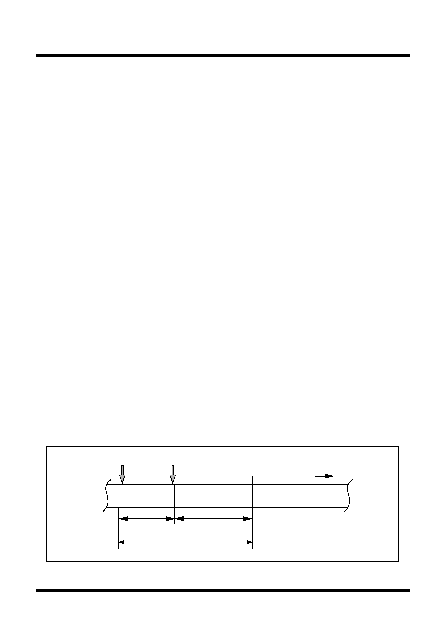
59
Tentative Specifications REV.A
Mitsubishi microcomputers
M16C / 62T Group
SINGLE-CHIP 16-BIT CMOS MICROCOMPUTER
S
pecifications in this manual are tentative and subject to change.
Under
development
Interrupt
Interrupt Sequence
An interrupt sequence -- what are performed over a period from the instant an interrupt is accepted to the
instant the interrupt routine is executed -- is described here.
If an interrupt occurs during execution of an instruction, the processor determines its priority when the
execution of the instruction is completed, and transfers control to the interrupt sequence from the next
cycle. If an interrupt occurs during execution of either the SMOVB, SMOVF, SSTR or RMPA instruction,
the processor temporarily suspends the instruction being executed, and transfers control to the interrupt
sequence.
In the interrupt sequence, the processor carries out the following in sequence given:
(1) CPU gets the interrupt information (the interrupt number and interrupt request level) by reading ad-
dress 00000
16
.
(2) Saves the content of the flag register (FLG) as it was immediately before the start of interrupt sequence
in the temporary register (Note) within the CPU.
(3) Sets the interrupt enable flag (I flag), the debug flag (D flag), and the stack pointer select flag (U flag) to
"0" (the U flag, however does not change if the INT instruction, in software interrupt numbers 32
through 63, is executed)
(4) Saves the content of the temporary register (Note) within the CPU in the stack area.
(5) Saves the content of the program counter (PC) in the stack area.
(6) Sets the interrupt priority level of the accepted instruction in the IPL.
After the interrupt sequence is completed, the processor resumes executing instructions from the first
address of the interrupt routine.
Note: This register cannot be utilized by the user.
Interrupt Response Time
'Interrupt response time' is the period between the instant an interrupt occurs and the instant the first
instruction within the interrupt routine has been executed. This time comprises the period from the
occurrence of an interrupt to the completion of the instruction under execution at that moment (a) and the
time required for executing the interrupt sequence (b). Figure 1.14.4 shows the interrupt response time.
Instruction
Interrupt sequence
Instruction in
interrupt routine
Time
Interrupt response time
(a)
(b)
Interrupt request acknowledged
Interrupt request generated
Figure 1.14.4. Interrupt response time
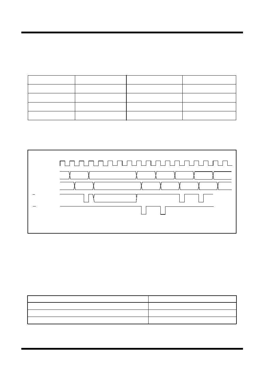
60
Tentative Specifications REV.A
Mitsubishi microcomputers
M16C / 62T Group
SINGLE-CHIP 16-BIT CMOS MICROCOMPUTER
S
pecifications in this manual are tentative and subject to change.
Under
development
Interrupt
Variation of IPL when Interrupt Request is Accepted
If an interrupt request is accepted, the interrupt priority level of the accepted interrupt is set in the IPL.
If an interrupt request, that does not have an interrupt priority level, is accepted, one of the values shown
in Table 1.14.6 is set in the IPL.
Stack pointer (SP) value
Interrupt vector address
16-Bit bus, without wait
8-Bit bus, without wait
Even
Even
Odd (Note 2)
Odd (Note 2)
Even
Odd
Even
Odd
18 cycles (Note 1)
19 cycles (Note 1)
19 cycles (Note 1)
20 cycles (Note 1)
20 cycles (Note 1)
20 cycles (Note 1)
20 cycles (Note 1)
20 cycles (Note 1)
Table 1.14.5. Time required for executing the interrupt sequence
Indeterminate
1
2
3
4
5
6
7
8
9
10
11
12
13
14
15
16
17
18
The indeterminate segment is dependent on the queue buffer.
If the queue buffer is ready to take an instruction, a read cycle occurs.
Indeterminate
SP-2
contents
SP-4
contents
vec
contents
vec+2
contents
Interrupt
information
Address
0000
Indeterminate
SP-2
SP-4
vec
vec+2
PC
BCLK
Address bus
Data bus
W
R
Time (a) is dependent on the instruction under execution. Thirty cycles is the maximum required for the
DIVX instruction (without wait).
Time (b) is as shown in Table 1.14.5.
________
Note 1: Add 2 cycles in the case of a DBC interrupt; add 1 cycle in the case either of an address coincidence
interrupt or of a single-step interrupt.
Note 2: Locate an interrupt vector address in an even address, if possible.
Figure 1.14.5. Time required for executing the interrupt sequence
Table 1.14.6. Relationship between interrupts without interrupt priority levels and IPL
Interrupt sources without priority levels
Value set in the IPL
_______
Watchdog timer, NMI
7
Reset
0
Other
Not changed
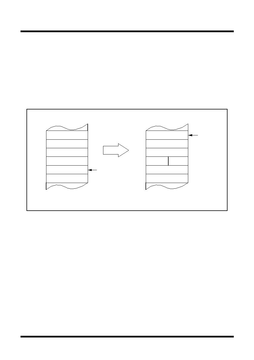
61
Tentative Specifications REV.A
Mitsubishi microcomputers
M16C / 62T Group
SINGLE-CHIP 16-BIT CMOS MICROCOMPUTER
S
pecifications in this manual are tentative and subject to change.
Under
development
Interrupt
Saving Registers
In the interrupt sequence, only the contents of the flag register (FLG) and that of the program counter
(PC) are saved in the stack area.
First, the processor saves the four higher-order bits of the program counter, and 4 upper-order bits and 8
lower-order bits of the FLG register, 16 bits in total, in the stack area, then saves 16 lower-order bits of the
program counter. Figure 1.14.6 shows the state of the stack as it was before the acceptance of the
interrupt request, and the state the stack after the acceptance of the interrupt request.
Save other necessary registers at the beginning of the interrupt routine using software. Using the
PUSHM instruction alone can save all the registers except the stack pointer (SP).
Address
Content of previous stack
Stack area
[SP]
Stack pointer
value before
interrupt occurs
m
m 1
m 2
m 3
m 4
Stack status before interrupt request
is acknowledged
Stack status after interrupt request
is acknowledged
Content of previous stack
m + 1
MSB
LSB
m
m 1
m 2
m 3
m 4
Address
Flag register (FLG
L
)
Content of previous stack
Stack area
Flag register
(FLG
H
)
Program
counter (PC
H
)
[SP]
New stack
pointer value
Content of previous stack
m + 1
MSB
LSB
Program counter (PC
L
)
Program counter (PC
M
)
Figure 1.14.6. State of stack before and after acceptance of interrupt request
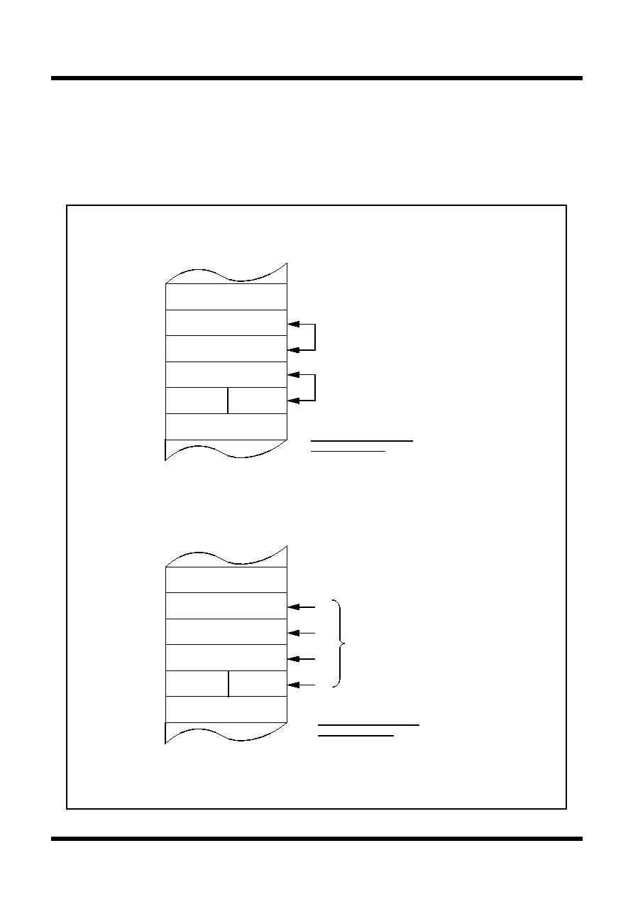
62
Tentative Specifications REV.A
Mitsubishi microcomputers
M16C / 62T Group
SINGLE-CHIP 16-BIT CMOS MICROCOMPUTER
S
pecifications in this manual are tentative and subject to change.
Under
development
Interrupt
Figure 1.14.7. Operation of saving registers
(2) Stack pointer (SP) contains odd number
[SP]
(Odd)
[SP] 1 (Even)
[SP] 2(Odd)
[SP] 3 (Even)
[SP] 4(Odd)
[SP] 5 (Even)
Address
Sequence in which order
registers are saved
(2)
(1)
Finished saving registers
in four operations.
(3)
(4)
(1) Stack pointer (SP) contains even number
[SP]
(Even)
[SP] 1(Odd)
[SP] 2 (Even)
[SP] 3(Odd)
[SP] 4 (Even)
[SP] 5 (Odd)
Note: [SP] denotes the initial value of the stack pointer (SP) when interrupt request is acknowledged.
After registers are saved, the SP content is [SP] minus 4.
Address
Program counter (PC
M
)
Stack area
Flag register (FLG
L
)
Program counter (PC
L
)
Sequence in which order
registers are saved
(2) Saved simultaneously,
all 16 bits
(1) Saved simultaneously,
all 16 bits
Finished saving registers
in two operations.
Program counter (PC
M
)
Stack area
Flag register (FLG
L
)
Program counter (PC
L
)
Saved simultaneously,
all 8 bits
Flag register
(FLG
H
)
Program
counter (PC
H
)
Flag register
(FLG
H
)
Program
counter (PC
H
)
The operation of saving registers carried out in the interrupt sequence is dependent on whether the
content of the stack pointer, at the time of acceptance of an interrupt request, is even or odd. If the
content of the stack pointer (Note) is even, the content of the flag register (FLG) and the content of the
program counter (PC) are saved, 16 bits at a time. If odd, their contents are saved in two steps, 8 bits at
a time. Figure 1.14.7 shows the operation of the saving registers.
Note: Stack pointer indicated by U flag.

63
Tentative Specifications REV.A
Mitsubishi microcomputers
M16C / 62T Group
SINGLE-CHIP 16-BIT CMOS MICROCOMPUTER
S
pecifications in this manual are tentative and subject to change.
Under
development
Interrupt
Interrupt Priority
If there are two or more interrupt requests occurring at a point in time within a single sampling (checking
whether interrupt requests are made), the interrupt assigned a higher priority is accepted.
Assign an arbitrary priority to maskable interrupts (peripheral I/O interrupts) using the interrupt priority level
select bit. If the same interrupt priority level is assigned, however, the interrupt assigned a higher hardware
priority is accepted.
Priorities of the special interrupts, such as Reset (dealt with as an interrupt assigned the highest priority),
watchdog timer interrupt, etc. are regulated by hardware.
Figure 1.14.8 shows the priorities of hardware interrupts.
Software interrupts are not affected by the interrupt priority. If an instruction is executed, control branches
invariably to the interrupt routine.
Returning from an Interrupt Routine
Executing the REIT instruction at the end of an interrupt routine returns the contents of the flag register
(FLG) as it was immediately before the start of interrupt sequence and the contents of the program counter
(PC), both of which have been saved in the stack area. Then control returns to the program that was being
executed before the acceptance of the interrupt request, so that the suspended process resumes.
Return the other registers saved by software within the interrupt routine using the POPM or similar instruc-
tion before executing the REIT instruction.
Interrupt resolution circuit
When two or more interrupts are generated simultaneously, this circuit selects the interrupt with the highest
priority level. Figure 1.14.9 shows the circuit that judges the interrupt priority level.
Figure 1.14.8. Hardware interrupts priorities
_______
________
Reset > NMI > DBC > Watchdog timer > Peripheral I/O > Single step > Address match
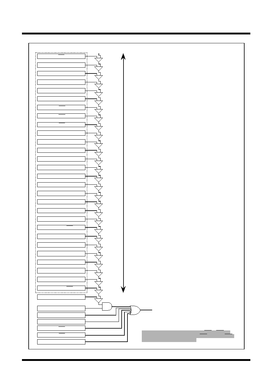
64
Tentative Specifications REV.A
Mitsubishi microcomputers
M16C / 62T Group
SINGLE-CHIP 16-BIT CMOS MICROCOMPUTER
S
pecifications in this manual are tentative and subject to change.
Under
development
Interrupt
Figure 1.14.9. Maskable interrupts priorities (peripheral I/O interrupts)
Timer B2
Timer B0
Timer A3
Timer A1
Timer B1
Timer A4
Timer A2
UART1 reception
UART0
reception
UART2 reception/ACK
A-D conversion
DMA1
Bus collision detection
Timer A0
UART1 transmission
UART0 transmission
UART2 transmission/NACK
Key input interrupt
DMA0
Processor interrupt priority level (IPL)
Interrupt enable flag (I flag)
INT1
INT2
INT0
Watchdog timer
Reset
DBC
NMI
Interrupt
request
accepted
Level 0 (initial value)
Priority level of each interrupt
High
Low
Priority of peripheral I/O interrupts
(if priority levels are same)
Timer B4
INT3
Timer B3
Timer B5
Serial I/O4/INT5
Serial I/O3/INT4
Address match
Note 1: In M30623 (80-pin package), can not use INT3 to INT5 as
the interrupt factors, because P1
5
/D
13
/INT3 to P1
7
/D
15
/INT5
have no corresponding external pin.
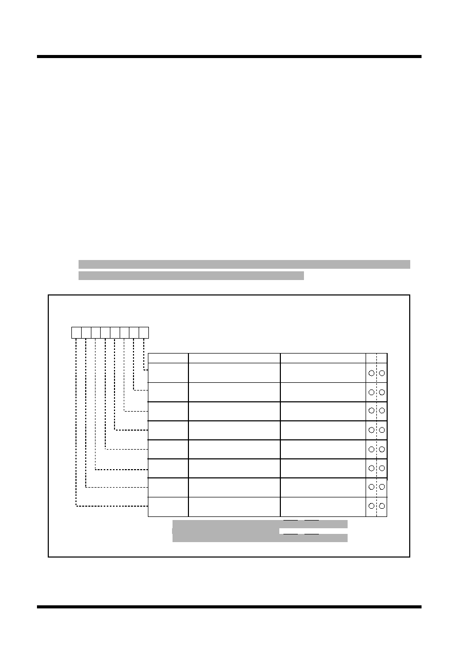
65
Tentative Specifications REV.A
Mitsubishi microcomputers
M16C / 62T Group
SINGLE-CHIP 16-BIT CMOS MICROCOMPUTER
S
pecifications in this manual are tentative and subject to change.
Under
development
______
INT Interrupt
________
________
INT0 to INT5 are triggered by the edges of external inputs. The edge polarity is selected using the polarity
select bit.
________
Of interrupt control registers, 0048
16
is used both as serial I/O4 and external interrupt INT5 input control
________
register, and 0049
16
is used both as serial I/O3 and as external interrupt INT4 input control register. Use the
interrupt request cause select bits - bits 6 and 7 of the interrupt request cause select register (035F
16
) - to
specify which interrupt request cause to select. After having set an interrupt request cause, be sure to clear
the corresponding interrupt request bit before enabling an interrupt.
Either of the interrupt control registers - 0048
16
, 0049
16
- has the polarity-switching bit. Be sure to set this bit
to "0" to select an serial I/O as the interrupt request cause.
As for external interrupt input, an interrupt can be generated both at the rising edge and at the falling edge
by setting "1" in the INTi interrupt polarity switching bit of the interrupt request cause select register
(035F
16
). To select both edges, set the polarity switching bit of the corresponding interrupt control register
to `falling edge' ("0").
Figure 1.14.10 shows the Interrupt request cause select register.
Note 1:
_______
_______
In M30623(80-pin package), can not use INT3
to INT5
as the interrupt factor, because
_______
_______
P1
5
/D
13
/INT
3
to P1
7
/D
15
/INT
5
have no corresponding external pin.
Figure 1.14.10. Interrupt request cause select register
Interrupt request cause select register
Bit name
Fumction
Bit symbol
W
R
Symbol
Address
When reset
IFSR
035F
16
00
16
IFSR0
b7
b6
b5
b4
b3
b2
b1
b0
INT0 interrupt polarity
swiching bit
0 : SIO3
1 : INT4
0 : SIO4
1 : INT5
0 : One edge
1 : Two edges
0 : One edge
1 : Two edges
0 : One edge
1 : Two edges
0 : One edge
1 : Two edges
0 : One edge
1 : Two edges
INT1 interrupt polarity
swiching bit
INT2 interrupt polarity
swiching bit
INT3 interrupt polarity
swiching bit
INT4 interrupt polarity
swiching bit
INT5 interrupt polarity
swiching bit
0 : One edge
1 : Two edges
Interrupt request cause
select bit
Interrupt request cause
select bit
IFSR1
IFSR2
IFSR3
IFSR4
IFSR5
IFSR6
IFSR7
Note 1: In M30623(80-pin package), can not use INT3 to INT5 interrupts,
so setting data of these bits are invalid.
Note 2: In M30623(80-pin package), can not use INT3 to INT5 interrupts.
______
INT Interrupt
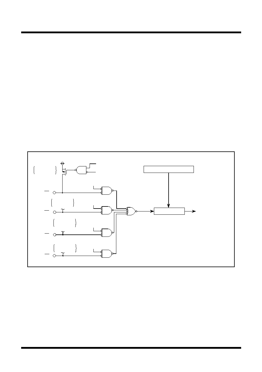
66
Tentative Specifications REV.A
Mitsubishi microcomputers
M16C / 62T Group
SINGLE-CHIP 16-BIT CMOS MICROCOMPUTER
S
pecifications in this manual are tentative and subject to change.
Under
development
Interrupt control circuit
Key input interrupt control register
(address 004D
16
)
Key input interrupt
request
P10
7
/KI
3
P10
6
/KI
2
P10
5
/KI
1
P10
4
/KI
0
Port P10
4
-P10
7
pull-up
select bit
Port P10
7
direction
register
Pull-up
transistor
Port P10
7
direction register
Port P10
6
direction
register
Port P10
5
direction
register
Port P10
4
direction
register
Pull-up
transistor
Pull-up
transistor
Pull-up
transistor
Figure 1.14.11. Block diagram of key input interrupt
______
NMI Interrupt
______
______
______
An NMI interrupt is generated when the input to the P8
5
/NMI pin changes from "H" to "L". The NMI interrupt
is a non-maskable external interrupt. The pin level can be checked in the port P8
5
register (bit 5 at address
03F0
16
).
This pin cannot be used as a normal port input.
Key Input Interrupt
If the direction register of any of P10
4
to P10
7
is set for input and a falling edge is input to that port, a key
input interrupt is generated. A key input interrupt can also be used as a key-on wakeup function for cancel-
ling the wait mode or stop mode. However, if you intend to use the key input interrupt, do not use P10
4
to
P10
7
as A-D input ports. Figure 1.14.11 shows the block diagram of the key input interrupt. Note that if an
"L" level is input to any pin that has not been disabled for input, inputs to the other pins are not detected as
an interrupt.
_______
NMI Interrupt
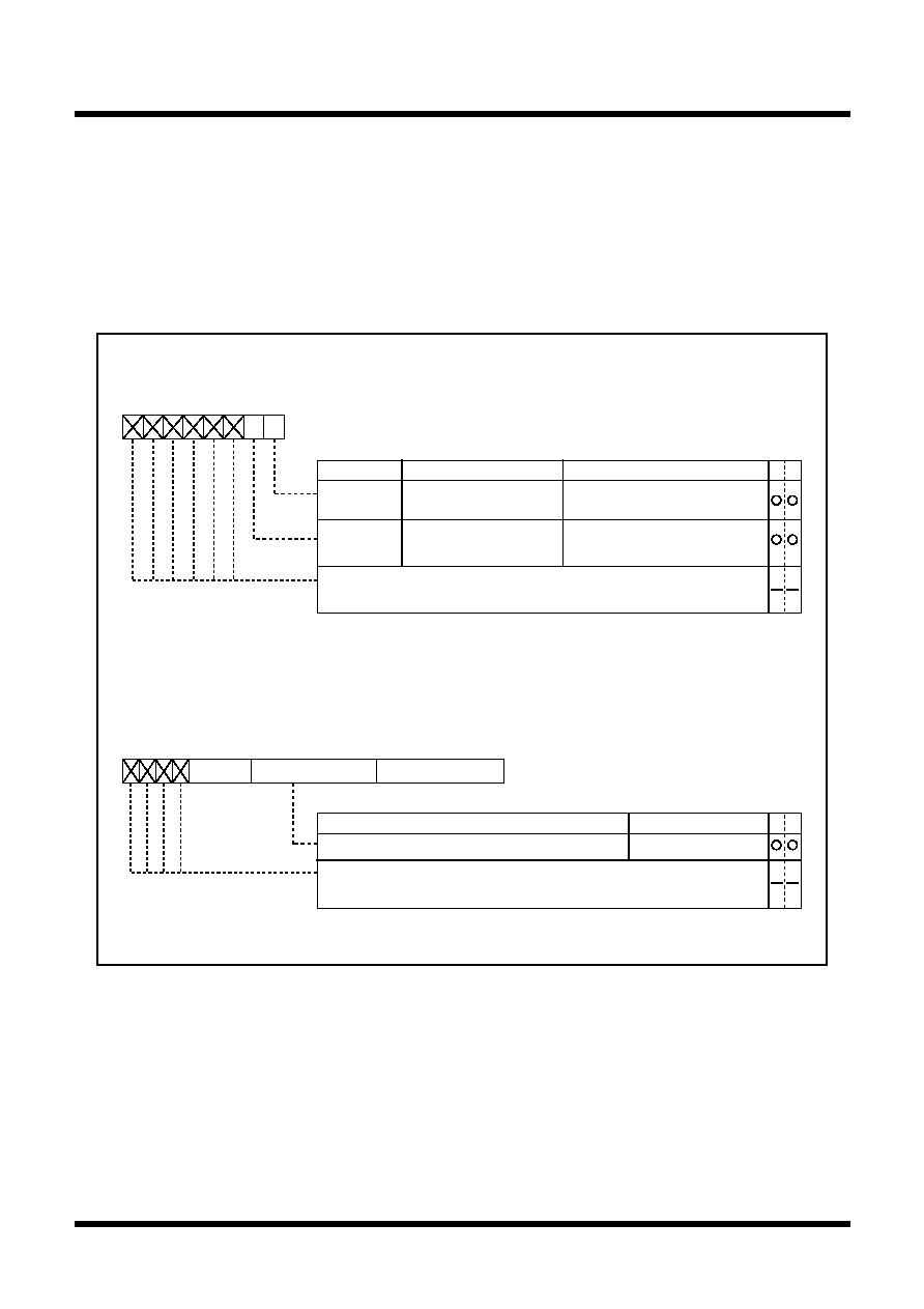
67
Tentative Specifications REV.A
Mitsubishi microcomputers
M16C / 62T Group
SINGLE-CHIP 16-BIT CMOS MICROCOMPUTER
S
pecifications in this manual are tentative and subject to change.
Under
development
Address Match Interrupt
An address match interrupt is generated when the address match interrupt address register contents match
the program counter value. Two address match interrupts can be set, each of which can be enabled and
disabled by an address match interrupt enable bit. Address match interrupts are not affected by the inter-
rupt enable flag (I flag) and processor interrupt priority level (IPL). The value of the program counter (PC)
for an address match interrupt varies depending on the instruction being executed.
Figure 1.14.12 shows the address match interrupt-related registers.
Bit name
Bit symbol
Symbol
Address When
reset
AIER
0009
16
XXXXXX00
2
Address match interrupt enable register
Function
W
R
Address match interrupt 0
enable bit
0 : Interrupt disabled
1 : Interrupt enabled
AIER0
Address match interrupt 1
enable bit
AIER1
Symbol
Address
When reset
RMAD0
0012
16
to 0010
16
X00000
16
RMAD1
0016
16
to 0014
16
X00000
16
Nothing is assigned.
In an attempt to write to these bits, write "0". The value, if read, turns out to
be indeterminated.
b7
b6
b5
b4
b3
b2
b1
b0
W
R
Address setting register for address match interrupt
Function
Values that can be set
Address match interrupt register i (i = 0, 1)
00000
16
to FFFFF
16
Nothing is assigned.
In an attempt to write to these bits, write "0". The value, if read, turns out to
be indeterminated.
0 : Interrupt disabled
1 : Interrupt enabled
b0 b7
b0
b3
(b19)
(b16)
b7
b0
(b15)
(b8)
b7
(b23)
Figure 1.14.12. Address match interrupt-related registers
Address Match Interrupt

68
Tentative Specifications REV.A
Mitsubishi microcomputers
M16C / 62T Group
SINGLE-CHIP 16-BIT CMOS MICROCOMPUTER
S
pecifications in this manual are tentative and subject to change.
Under
development
Precautions for Interrupts
(1) Reading address 00000
16
· When maskable interrupt is occurred, CPU read the interrupt information (the interrupt number and
interrupt request level) in the interrupt sequence.
The interrupt request bit of the certain interrupt written in address 00000
16
will then be set to "0".
Reading address 00000
16
by software sets enabled highest priority interrupt source request bit to "0".
Though the interrupt is generated, the interrupt routine may not be executed.
Do not read address 00000
16
by software.
(2) Setting the stack pointer
· The value of the stack pointer immediately after reset is initialized to 0000
16
. Accepting an interrupt
before setting a value in the stack pointer may become a factor of runaway. Be sure to set a value in
_______
the stack pointer before accepting an interrupt. When using the NMI interrupt, initialize the stack point
at the beginning of a program. Concerning the first instruction immediately after reset, generating any
_______
interrupts including the NMI interrupt is prohibited.
_______
(3) The NMI interrupt
_______
· As for the NMI interrupt pin, an interrupt cannot be disabled. Connect it to the Vcc pin via a resistor
(pull-up) if unused. Be sure to work on it.
_______
· The NMI pin also serves as P8
5
, which is exclusively input. Reading the contents of the P8 register
allows reading the pin value. Use the reading of this pin only for establishing the pin level at the time
_______
when the NMI interrupt is input.
_______
· Do not reset the CPU with the input to the NMI pin being in the "L" state.
_______
· Do not attempt to go into stop mode with the input to the NMI pin being in the "L" state. With the input to
_______
the NMI being in the "L" state, the CM10 is fixed to "0", so attempting to go into stop mode is turned
down.
_______
· Do not attempt to go into wait mode with the input to the NMI pin being in the "L" state. With the input to
_______
the NMI pin being in the "L" state, the CPU stops but the oscillation does not stop, so no power is saved.
In this instance, the CPU is returned to the normal state by a later interrupt.
_______
· Signals input to the NMI pin require an "L" level of 1 clock or more, from the operation clock of the CPU.
(4) External interrupt
________
· Either an "L" level or an "H" level of at least 250 ns width is necessary for the signal input to pins INT
0
________
through INT
5
regardless of the CPU operation clock.
________
________
· When the polarity of the INT
0
to INT
5
pins is changed, the interrupt request bit is sometimes set to "1".
After changing the polarity, set the interrupt request bit to "0". Figure 1.14.13 shows the procedure for
______
changing the INT interrupt generate factor.
Note 1:
_______
_______
In M30623(80-pin package), can not use INT3
to INT5
as the interrupt factor,because
_______
_______
P1
5
/D
13
/INT
3
to P1
7
/D
15
/INT
5
have no corresponding external pin.
Precautions for Interrupts
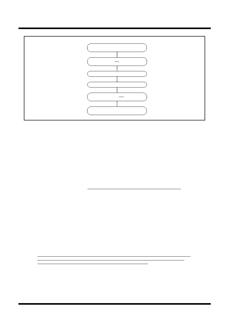
69
Tentative Specifications REV.A
Mitsubishi microcomputers
M16C / 62T Group
SINGLE-CHIP 16-BIT CMOS MICROCOMPUTER
S
pecifications in this manual are tentative and subject to change.
Under
development
______
Figure 1.14.13. Switching condition of INT interrupt request
Set the polarity select bit
Clear the interrupt request bit to "0"
Set the interrupt priority level to level 1 to 7
(Enable the accepting of INTi interrupt request)
Set the interrupt priority level to level 0
(Disable
INTi
interrupt)
Clear the interrupt enable flag to "0"
(Disable interrupt)
Set the interrupt enable flag to "1"
(Enable interrupt)
Precautions for Interrupts
Example 1:
INT_SWITCH1:
FCLR
I
; Disable interrupts.
AND.B
#00h, 0055h
; Clear TA0IC int. priority level and int. request bit.
NOP
; Four NOP instructions are required when using HOLD function.
NOP
FSET
I
; Enable interrupts.
Example 2:
INT_SWITCH2:
FCLR
I
; Disable interrupts.
AND.B
#00h, 0055h
; Clear TA0IC int. priority level and int. request bit.
MOV.W MEM, R0
; Dummy read.
FSET
I
; Enable interrupts.
Example 3:
INT_SWITCH3:
PUSHC FLG
; Push Flag register onto stack
FCLR
I
; Disable interrupts.
AND.B
#00h, 0055h
; Clear TA0IC int. priority level and int. request bit.
POPC
FLG
; Enable interrupts.
The reason why two NOP instructions (four when using the HOLD function) or dummy read are inserted
before FSET I in Examples 1 and 2 is to prevent the interrupt enable flag I from being set before the
interrupt control register is rewritten due to effects of the instruction queue.
(5) Rewrite the interrupt control register
· To rewrite the interrupt control register, do so at a point that does not generate the interrupt request for
that register. If there is possibility of the interrupt request occur, rewrite the interrupt control register after
the interrupt is disabled. The program examples are described as follow:
· When a instruction to rewrite the interrupt control register is executed but the interrupt is disabled, the
interrupt request bit is not set sometimes even if the interrupt request for that register has been gener-
ated. This will depend on the instruction. If this creates problems, use the below instructions to change
the register.
Instructions : AND, OR, BCLR, BSET
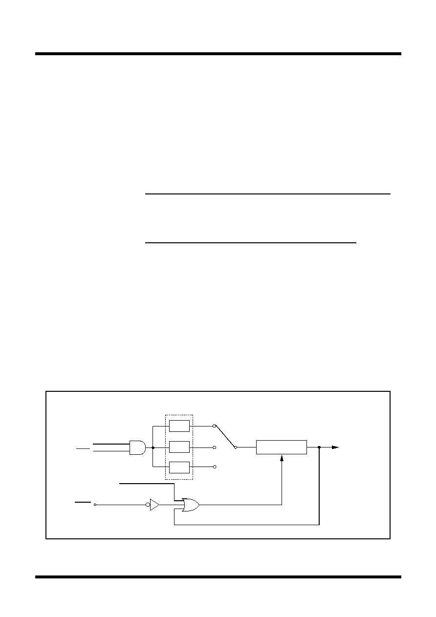
70
Tentative Specifications REV.A
Mitsubishi microcomputers
M16C / 62T Group
SINGLE-CHIP 16-BIT CMOS MICROCOMPUTER
S
pecifications in this manual are tentative and subject to change.
Under
development
Watchdog Timer
Watchdog Timer
The watchdog timer has the function of detecting when the program is out of control. The watchdog timer is
a 15-bit counter which down-counts the clock derived by dividing the BCLK using the prescaler. A watchdog
timer interrupt is generated when an underflow occurs in the watchdog timer. When X
IN
is selected for the
BCLK
,
bit 7 of the watchdog timer control register (address 000F
16
) selects the prescaler division ratio (by
16 or by 128). When X
CIN
is selected as the BCLK, the prescaler is set for division by 2 regardless of bit 7
of the watchdog timer control register (address 000F
16
). Thus the watchdog timer's period can be calcu-
lated as given below. The watchdog timer's period is, however, subject to an error due to the pre-scaler.
BCLK
Write to the watchdog timer
start register
(address 000E
16
)
RESET
Watchdog timer
interrupt request
Watchdog timer
Set to
"7FFF
16
"
1/128
1/16
"CM07 = 0"
"WDC7 = 1"
"CM07 = 0"
"WDC7 = 0"
"CM07 = 1"
HOLD
1/2
Prescaler
For example, suppose that BCLK runs at 10 MHz and that 16 has been chosen for the dividing ratio of the
pre-scaler, then the watchdog timer's period becomes approximately 52.4 ms.
The watchdog timer is initialized by writing to the watchdog timer start register (address 000E
16
) and when
a watchdog timer interrupt request is generated. The prescaler is initialized only when the microcomputer is
reset. After a reset is cancelled, the watchdog timer and prescaler are both stopped. The count is started by
writing to the watchdog timer start register (address 000E
16
).
Figure 1.15.1 shows the block diagram of the watchdog timer. Figure 1.15.2 shows the watchdog timer-
related registers.
With X
IN
chosen for BCLK
Watchdog timer period =
pre-scaler dividing ratio (16 or 128) X watchdog timer count (32768)
BCLK
Figure 1.15.1. Block diagram of watchdog timer
With X
CIN
chosen for BCLK
Watchdog timer period =
pre-scaler dividing ratio (2) X watchdog timer count (32768)
BCLK
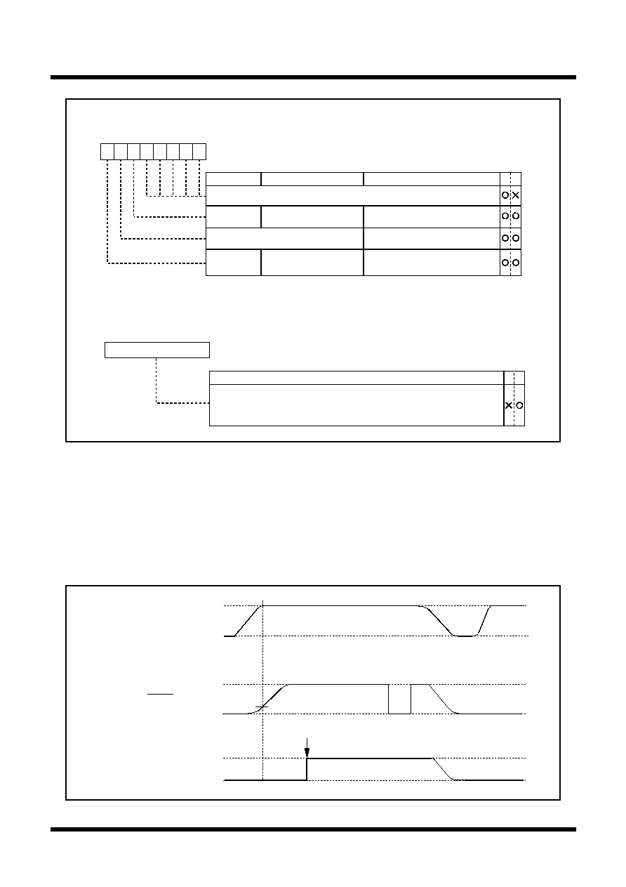
71
Tentative Specifications REV.A
Mitsubishi microcomputers
M16C / 62T Group
SINGLE-CHIP 16-BIT CMOS MICROCOMPUTER
S
pecifications in this manual are tentative and subject to change.
Under
development
Watchdog Timer
Watchdog timer control register
Symbol
Address
When reset
WDC
000F
16
00
V
XXXXX
2
Function
Bit symbol
W
R
b7
b6
b5
b4
b3
b2
b1
b0
High-order bit of watchdog timer
WDC7
Bit name
Prescaler select bit
0 : Divided by 16
1 : Divided by 128
Watchdog timer start register
Symbol
Address
When reset
WDTS
000E
16
Indeterminate
W
R
b7
b0
Function
The watchdog timer is initialized and starts counting after a write instruction to
this register. The watchdog timer value is always initialized to "7FFF
16
"
regardless of whatever value is written.
Reserved bit
Must always be set to "0"
0
0
WDV5
0 : Cold start
1 : Warm start
Note 1: When this flag is written ``0'' or ``1'', it is set ``1'' automatically .
V
: This bit is not under the influence of a reset.
Cold start / warm start
discrimination flag (Note 1)
Figure 1.15.2. Watchdog timer control and start registers
Cold start / Warm start
The cold start/warm start discrimination flag(bit 5 at 000F
16
) indicates the last reset by power on(cold start)
or by reset signal(warm start).
The cold start/warm start discrimination flag is set ``0'' at power on, and is set ``1'' at writing any data to the
watchdog timer control register(address is 000F
16
). The flag is not set to ``0'' by the software reset and the
input of reset signal.
Figure 1.15.3. Cold sgtart / Warm start
Vcc
``5V''
``0V''
``0V''
``5V''
``1''
``0''
Cold start / Warm start
discrimination flag (WDC5)
RESET
0.2Vcc
Set to ``1'' by software
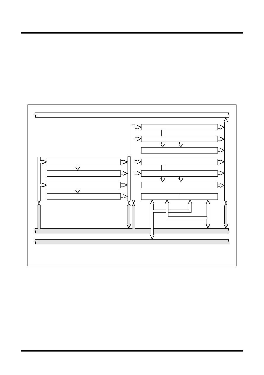
72
Mitsubishi microcomputers
M16C / 62T Group
SINGLE-CHIP 16-BIT CMOS MICROCOMPUTER
DMAC
DMAC
This microcomputer has two DMAC (direct memory access controller) channels that allow data to be sent to
memory without using the CPU. DMAC shares the same data bus with the CPU. The DMAC is given a
higher right of using the bus than the CPU, which leads to working the cycle stealing method. On this
account, the operation from the occurrence of DMA transfer request signal to the completion of 1-word (16-
bit) or 1-byte (8-bit) data transfer can be performed at high speed. Figure 1.16.1 shows the block diagram
of the DMAC. Table 1.16.1 shows the DMAC specifications. Figures 1.16.2 to 1.16.4 show the registers
used by the DMAC.
Figure 1.16.1. Block diagram of DMAC
Data bus low-order bits
DMA latch high-order bits
DMA latch low-order bits
DMA0 source pointer SAR0(20)
DMA0 destination pointer DAR0 (20)
DMA0 forward address pointer (20) (Note)
Data bus high-order bits
Address bus
DMA1 destination pointer DAR1 (20)
DMA1 source pointer SAR1 (20)
DMA1 forward address pointer (20) (Note)
DMA0 transfer counter reload register TCR0 (16)
DMA0 transfer counter TCR0 (16)
DMA1 transfer counter reload register TCR1 (16)
DMA1 transfer counter TCR1 (16)
(addresses 0029
16
, 0028
16
)
(addresses 0039
16
, 0038
16
)
(addresses 0022
16
to 0020
16
)
(addresses 0026
16
to 0024
16
)
(addresses 0032
16
to 0030
16
)
(addresses 0036
16
to 0034
16
)
Note: Pointer is incremented by a DMA request.
Either a write signal to the software DMA request bit or an interrupt request signal is used as a DMA transfer
request signal. But the DMA transfer is affected neither by the interrupt enable flag (I flag) nor by the
interrupt priority level. The DMA transfer doesn't affect any interrupts either.
If the DMAC is active (the DMA enable bit is set to 1), data transfer starts every time a DMA transfer request
signal occurs. If the cycle of the occurrences of DMA transfer request signals is higher than the DMA
transfer cycle, there can be instances in which the number of transfer requests doesn't agree with the
number of transfers. For details, see the description of the DMA request bit.
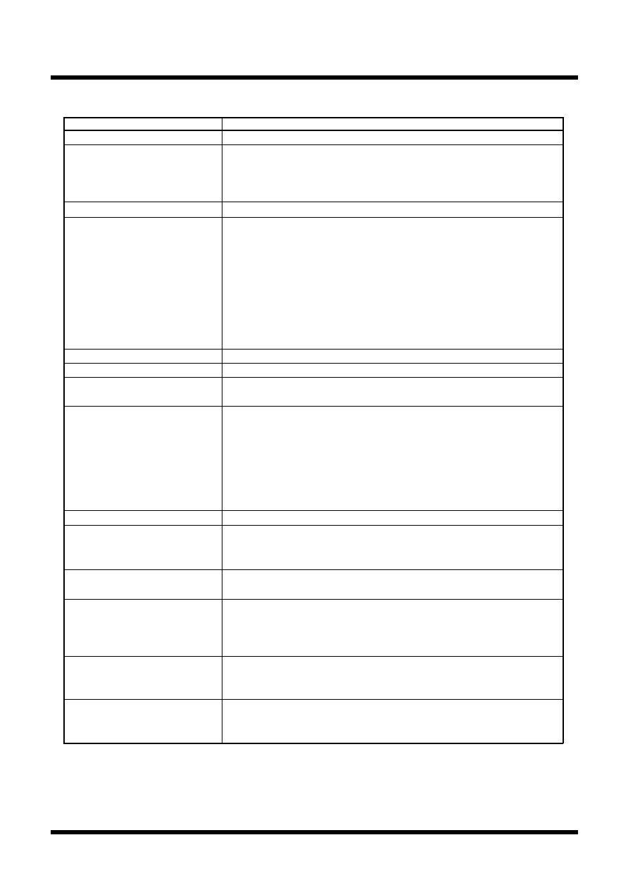
73
Mitsubishi microcomputers
M16C / 62T Group
SINGLE-CHIP 16-BIT CMOS MICROCOMPUTER
DMAC
Item
Specification
No. of channels
2 (cycle steal method)
Transfer memory space
· From any address in the 1M bytes space to a fixed address
· From a fixed address to any address in the 1M bytes space
· From a fixed address to a fixed address
(Note that DMA-related registers [0020
16
to 003F
16
] cannot be accessed)
Maximum No. of bytes transferred
128K bytes (with 16-bit transfers) or 64K bytes (with 8-bit transfers)
DMA request factors (Note)
________
________ ________
________
Falling edge of INT0 or INT1 (INT0 can be selected by DMA0, INT1 by DMA1) or both edge
Timer A0 to timer A4 interrupt requests
Timer B0 to timer B5 interrupt requests
UART0 transfer and reception interrupt requests
UART1 transfer and reception interrupt requests
UART2 transfer and reception interrupt requests
Serial I/O3, 4 interrpt requests
A-D conversion interrupt requests
Software triggers
Channel priority
DMA0 takes precedence if DMA0 and DMA1 requests are generated simultaneously
Transfer unit
8 bits or 16 bits
Transfer address direction
forward/fixed (forward direction cannot be specified for both source and
destination simultaneously)
Transfer mode
· Single transfer mode
After the transfer counter underflows, the DMA enable bit turns to
"0", and the DMAC turns inactive
· Repeat transfer mode
After the transfer counter underflows, the value of the transfer counter
reload register is reloaded to the transfer counter.
The DMAC remains active unless a "0" is written to the DMA enable bit.
DMA interrupt request generation timing When an underflow occurs in the transfer counter
Active
When the DMA enable bit is set to "1", the DMAC is active.
When the DMAC is active, data transfer starts every time a DMA
transfer request signal occurs.
Inactive
· When the DMA enable bit is set to "0", the DMAC is inactive.
· After the transfer counter underflows in single transfer mode
At the time of starting data transfer immediately after turning the DMAC active, the
value of one of source pointer and destination pointer - the one specified for the
forward direction - is reloaded to the forward direction address pointer,and the value
of the transfer counter reload register is reloaded to the transfer counter.
Writing to register
Registers specified for forward direction transfer are always write enabled.
Registers specified for fixed address transfer are write-enabled when
the DMA enable bit is "0".
Reading the register
Can be read at any time.
However, when the DMA enable bit is "1", reading the register set up as the
forward register is the same as reading the value of the forward address pointer.
Table 1.16.1. DMAC specifications
Note: DMA transfer is not effective to any interrupt. DMA transfer is affected neither by the interrupt enable
flag (I flag) nor by the interrupt priority level.
Forward address pointer and
reload timing for transfer
counter
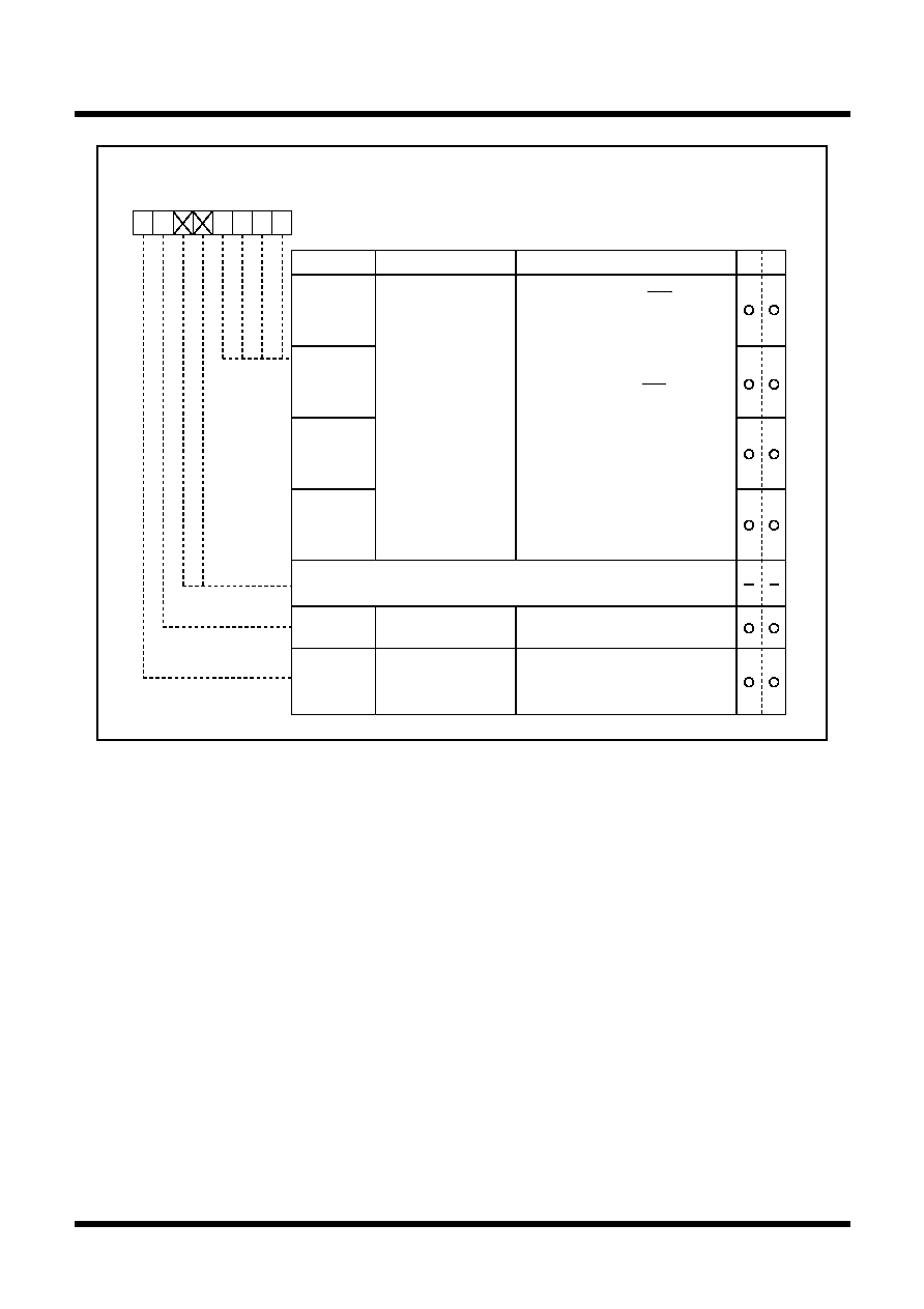
74
Mitsubishi microcomputers
M16C / 62T Group
SINGLE-CHIP 16-BIT CMOS MICROCOMPUTER
DMAC
DMA0 request cause select register
Symbol
Address
When reset
DM0SL
03B8
16
00
16
Function
Bit symbol
b7
b6
b5
b4
b3
b2
b1
b0
DMA request cause
select bit
DSEL0
R
W
DSEL1
DSEL2
DSEL3
Nothing is assigned.
In an attempt to write to these bits, write "0". The value, if read, turns out to be "0".
Software DMA
request bit
If software trigger is selected, a
DMA request is generated by
setting this bit to "1" (When read,
the value of this bit is always "0")
DSR
b3 b2 b1 b0
0 0 0 0 : Falling edge of INT0 pin
0 0 0 1 : Software trigger
0 0 1 0 : Timer A0
0 0 1 1 : Timer A1
0 1 0 0 : Timer A2
0 1 0 1 : Timer A3
0 1 1 0 : Timer A4 (DMS=0)
/two edges of INT0 pin (DMS=1)
0 1 1 1 : Timer B0 (DMS=0)
Timer B3 (DMS=1)
1 0 0 0 : Timer B1 (DMS=0)
Timer B4 (DMS=1)
1 0 0 1 : Timer B2 (DMS=0)
Timer B5 (DMS=1)
1 0 1 0 : UART0 transmit
1 0 1 1 : UART0 receive
1 1 0 0 : UART2 transmit
1 1 0 1 : UART2 receive
1 1 1 0 : A-D conversion
1 1 1 1 : UART1 transmit
Bit name
DMA request cause
expansion bit
DMS
0 : Normal
1 : Expanded cause
Figure 1.16.2. DMAC register (1)
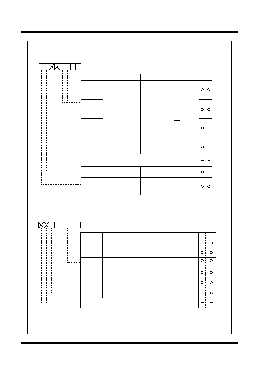
75
Mitsubishi microcomputers
M16C / 62T Group
SINGLE-CHIP 16-BIT CMOS MICROCOMPUTER
DMAC
DMAi control register
Symbol
Address
When reset
DMiCON(i=0,1)
002C
16
, 003C
16
00000X00
2
Bit name
Function
Bit symbol
Transfer unit bit select bit
b7
b6
b5
b4
b3
b2
b1
b0
0 : 16 bits
1 : 8 bits
DMBIT
R
W
DMASL
DMAS
DMAE
Repeat transfer mode
select bit
0 : Single transfer
1 : Repeat transfer
DMA request bit (Note 1)
0 : DMA not requested
1 : DMA requested
0 : Disabled
1 : Enabled
0 : Fixed
1 : Forward
DMA enable bit
Source address direction
select bit (Note 3)
Destination address
direction select bit (Note 3)
0 : Fixed
1 : Forward
DSD
DAD
Nothing is assigned.
In an attempt to write to these bits, write "0". The value, if read, turns out to be "0".
Note 1: DMA request can be cleared by resetting the bit.
Note 2: This bit can only be set to "0".
Note 3: Source address direction select bit and destination address direction select bit
cannot be set to "1" simultaneously.
(Note 2)
DMA1 request cause select register
Symbol
Address
When reset
DM1SL
03BA
16
00
16
Function
Bit symbol
b7
b6
b5
b4
b3
b2
b1
b0
DMA request cause
select bit
DSEL0
R
W
DSEL1
DSEL2
DSEL3
Nothing is assigned.
In an attempt to write to these bits, write "0". The value, if read, turns out to be "0".
Software DMA
request bit
If software trigger is selected, a
DMA request is generated by
setting this bit to "1" (When read,
the value of this bit is always "0")
DSR
b3 b2 b1 b0
0 0 0 0 : Falling edge of INT1 pin
0 0 0 1 : Software trigger
0 0 1 0 : Timer A0
0 0 1 1 : Timer A1
0 1 0 0 : Timer A2
0 1 0 1 : Timer A3(DMS=0)
/serial I/O3 (DMS=1)
0 1 1 0 : Timer A4 (DMS=0)
/serial I/O4 (DMS=1)
0 1 1 1 : Timer B0 (DMS=0)
/two edges of INT1 (DMS=1)
1 0 0 0 : Timer B1
1 0 0 1 : Timer B2
1 0 1 0 : UART0 transmit
1 0 1 1 : UART0 receive
1 1 0 0 : UART2 transmit
1 1 0 1 : UART2 receive
1 1 1 0 : A-D conversion
1 1 1 1 : UART1 receive
Bit name
DMA request cause
expansion bit
DMS
0 : Normal
1 : Expanded cause
Figure 1.16.3. DMAC register (2)
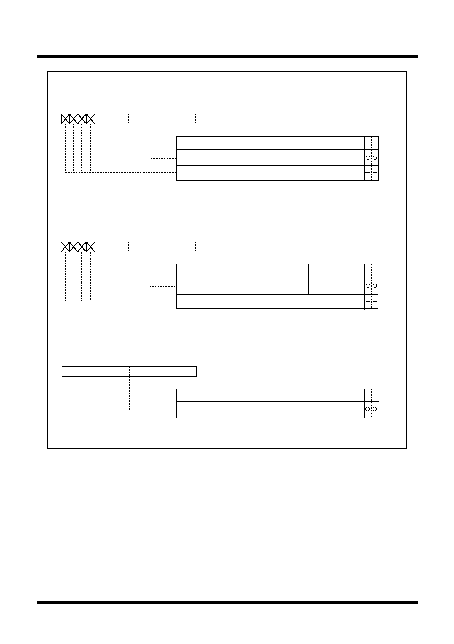
76
Mitsubishi microcomputers
M16C / 62T Group
SINGLE-CHIP 16-BIT CMOS MICROCOMPUTER
DMAC
b7
b0
b7
b0
(b8)
(b15)
Function
R W
· Transfer counter
Set a value one less than the transfer count
Symbol
Address
When reset
TCR0
0029
16
, 0028
16
Indeterminate
TCR1
0039
16
, 0038
16
Indeterminate
DMAi transfer counter (i = 0, 1)
Transfer count
specification
0000
16
to FFFF
16
b7
(b23)
b3
b0
b7
b0
b7
b0
(b8)
(b16)(b15)
(b19)
Function
R W
· Source pointer
Stores the source address
Symbol
Address
When reset
SAR0
0022
16
to 0020
16
Indeterminate
SAR1
0032
16
to 0030
16
Indeterminate
DMAi source pointer (i = 0, 1)
Transfer count
specification
00000
16
to FFFFF
16
Nothing is assigned.
In an attempt to write to these bits, write "0". The value, if read, turns out to be "0".
Symbol
Address
When reset
DAR0
0026
16
to 0024
16
Indeterminate
DAR1
0036
16
to 0034
16
Indeterminate
b3
b0
b7
b0
b7
b0
(b8)
(b15)
(b16)
(b19)
Function
R W
· Destination pointer
Stores the destination address
DMAi destination pointer (i = 0, 1)
Transfer count
specification
00000
16
to FFFFF
16
b7
(b23)
Nothing is assigned.
In an attempt to write to these bits, write "0". The value, if read, turns out to be "0".
Figure 1.16.4. DMAC register (3)

77
Mitsubishi microcomputers
M16C / 62T Group
SINGLE-CHIP 16-BIT CMOS MICROCOMPUTER
DMAC
(1) Transfer cycle
The transfer cycle consists of the bus cycle in which data is read from memory or from the SFR area
(source read) and the bus cycle in which the data is written to memory or to the SFR area (destination
write). The number of read and write bus cycles depends on the source and destination addresses. In
memory expansion mode and microprocessor mode, the number of read and write bus cycles also de-
pends on the level of the BYTE pin. Also, the bus cycle itself is longer when software waits are inserted.
(a) Effect of source and destination addresses
When 16-bit data is transferred on a 16-bit data bus, and the source and destination both start at odd
addresses, there are one more source read cycle and destination write cycle than when the source
and destination both start at even addresses.
(b) Effect of BYTE pin level
When transferring 16-bit data over an 8-bit data bus (BYTE pin = "H") in memory expansion mode and
microprocessor mode, the 16 bits of data are sent in two 8-bit blocks. Therefore, two bus cycles are
required for reading the data and two are required for writing the data. Also, in contrast to when the
CPU accesses internal memory, when the DMAC accesses internal memory (internal ROM, internal
RAM, and SFR), these areas are accessed using the data size selected by the BYTE pin.
(c) Effect of software wait
When the SFR area or a memory area with a software wait is accessed, the number of cycles is
increased for the wait by 1 bus cycle. The length of the cycle is determined by BCLK.
Figure 1.16.5 shows the example of the transfer cycles for a source read. For convenience, the destina-
tion write cycle is shown as one cycle and the source read cycles for the different conditions are shown.
In reality, the destination write cycle is subject to the same conditions as the source read cycle, with the
transfer cycle changing accordingly. When calculating the transfer cycle, remember to apply the respec-
tive conditions to both the destination write cycle and the source read cycle. For example (2) in Figure
1.16.5, if data is being transferred in 16-bit units on an 8-bit bus, two bus cycles are required for both the
source read cycle and the destination write cycle.
Note 1: M30623(80-pin package), in case of access to the external bus area, can be used only when 8-bit
bus mode.
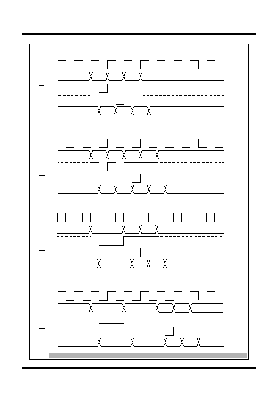
78
Mitsubishi microcomputers
M16C / 62T Group
SINGLE-CHIP 16-BIT CMOS MICROCOMPUTER
DMAC
BCLK
Address
bus
RD signal
WR signal
Data
bus
CPU use
CPU use
CPU use
CPU use
Source
Source
Destination
Destination
Dummy
cycle
Dummy
cycle
(1) 8-bit transfers
16-bit transfers from even address and the source address is even.
BCLK
Address
bus
RD signal
WR signal
Data
bus
CPU use
CPU use
CPU use
CPU use
Source
Source
Destination
Destination
Dummy
cycle
Dummy
cycle
(3) One wait is inserted into the source read under the conditions in (1)
BCLK
Address
bus
RD signal
WR signal
Data
bus
CPU use
CPU use
CPU use
CPU use
Source
Source
Destination
Destination
Dummy
cycle
Dummy
cycle
Source + 1
Source + 1
(2) 16-bit transfers and the source address is odd
Transferring 16-bit data on an 8-bit data bus (In this case, there are also two destination write cycles).
BCLK
Address
bus
RD signal
WR signal
Data
bus
CPU use
CPU use
CPU use
CPU use
Source
Source
Destination
Destination
Dummy
cycle
Dummy
cycle
Source + 1
Source + 1
(4) One wait is inserted into the source read under the conditions in (2)
(When 16-bit data is transferred on an 8-bit data bus, there are two destination write cycles).
Note 1: The same timing changes occur with the respective conditions at the destination as at the source.
Note 2: M30623(80-pin package), in case of access to the external bus area, can be used only when 8-bit bus mode.
Figure 1.16.5. Example of the transfer cycles for a source read
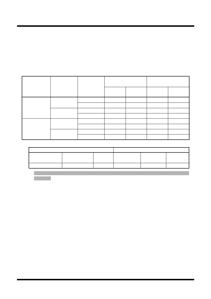
79
Mitsubishi microcomputers
M16C / 62T Group
SINGLE-CHIP 16-BIT CMOS MICROCOMPUTER
DMAC
Single-chip mode
Memory expansion mode
Transfer unit
Bus width
Access address
Microprocessor mode
No. of read
No. of write
No. of read No. of write
cycles
cycles
cycles
cycles
16-bit
Even
1
1
1
1
8-bit transfers
(BYTE= "L")
Odd
1
1
1
1
(DMBIT= "1")
8-bit
Even
--
--
1
1
(BYTE = "H")
Odd
--
--
1
1
16-bit
Even
1
1
1
1
16-bit transfers
(BYTE = "L")
Odd
2
2
2
2
(DMBIT= "0")
8-bit
Even
--
--
2
2
(BYTE = "H")
Odd
--
--
2
2
Table 1.16.2. No. of DMAC transfer cycles
Internal memory
External memory
Internal ROM/RAM
Internal ROM/RAM
SFR area
Separate bus
Separate bus
Multiplex
No wait
With wait
No wait
With wait
bus
1
2
2
1
2
3
Coefficient j, k
(2) DMAC transfer cycles
Any combination of even or odd transfer read and write addresses is possible. Table 1.16.2 shows the
number of DMAC transfer cycles.
The number of DMAC transfer cycles can be calculated as follows:
No. of transfer cycles per transfer unit = No. of read cycles x j + No. of write cycles x k
Note 1: M30623(80-pin package), in case of access to the external bus area, can be used only when 8-bit
bus mode.

80
Mitsubishi microcomputers
M16C / 62T Group
SINGLE-CHIP 16-BIT CMOS MICROCOMPUTER
DMAC
DMA enable bit
Setting the DMA enable bit to "1" makes the DMAC active. The DMAC carries out the following operations
at the time data transfer starts immediately after DMAC is turned active.
(1) Reloads the value of one of the source pointer and the destination pointer - the one specified for the
forward direction - to the forward direction address pointer.
(2) Reloads the value of the transfer counter reload register to the transfer counter.
Thus overwriting "1" to the DMA enable bit with the DMAC being active carries out the operations given
above, so the DMAC operates again from the initial state at the instant "1" is overwritten to the DMA enable
bit.
DMA request bit
The DMAC can generate a DMA transfer request signal triggered by a factor chosen in advance out of DMA
request factors for each channel.
DMA request factors include the following.
* Factors effected by using the interrupt request signals from the built-in peripheral functions and software
DMA factors (internal factors) effected by a program.
* External factors effected by utilizing the input from external interrupt signals.
For the selection of DMA request factors, see the descriptions of the DMAi factor selection register.
The DMA request bit turns to "1" if the DMA transfer request signal occurs regardless of the DMAC's state
(regardless of whether the DMA enable bit is set "1" or to "0"). It turns to "0" immediately before data
transfer starts.
In addition, it can be set to "0" by use of a program, but cannot be set to "1".
There can be instances in which a change in DMA request factor selection bit causes the DMA request bit
to turn to "1". So be sure to set the DMA request bit to "0" after the DMA request factor selection bit is
changed.
The DMA request bit turns to "1" if a DMA transfer request signal occurs, and turns to "0" immediately
before data transfer starts. If the DMAC is active, data transfer starts immediately, so the value of the DMA
request bit, if read by use of a program, turns out to be "0" in most cases. To examine whether the DMAC
is active, read the DMA enable bit.
Here follows the timing of changes in the DMA request bit.
(1) Internal factors
Except the DMA request factors triggered by software, the timing for the DMA request bit to turn to "1" due
to an internal factor is the same as the timing for the interrupt request bit of the interrupt control register to
turn to "1" due to several factors.
Turning the DMA request bit to "1" due to an internal factor is timed to be effected immediately before the
transfer starts.
(2) External factors
An external factor is a factor caused to occur by the leading edge of input from the INTi pin (i depends on
which DMAC channel is used).
Selecting the INTi pins as external factors using the DMA request factor selection bit causes input from
these pins to become the DMA transfer request signals.
The timing for the DMA request bit to turn to "1" when an external factor is selected synchronizes with the
signal's edge applicable to the function specified by the DMA request factor selection bit (synchronizes
with the trailing edge of the input signal to each INTi pin, for example).
With an external factor selected, the DMA request bit is timed to turn to "0" immediately before data
transfer starts similarly to the state in which an internal factor is selected.
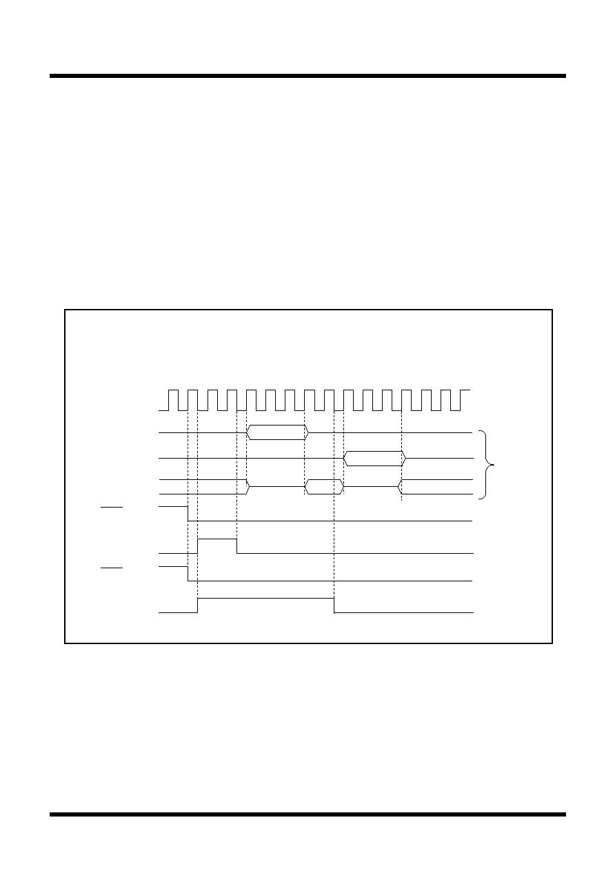
81
Mitsubishi microcomputers
M16C / 62T Group
SINGLE-CHIP 16-BIT CMOS MICROCOMPUTER
DMAC
(3) The priorities of channels and DMA transfer timing
If a DMA transfer request signal falls on a single sampling cycle (a sampling cycle means one period from
the leading edge to the trailing edge of BCLK), the DMA request bits of applicable channels concurrently
turn to "1". If the channels are active at that moment, DMA0 is given a high priority to start data transfer.
When DMA0 finishes data transfer, it gives the bus right to the CPU. When the CPU finishes single bus
access, then DMA1 starts data transfer and gives the bus right to the CPU.
An example in which DMA transfer is carried out in minimum cycles at the time when DMA transfer
request signals due to external factors concurrently occur.
Figure 1.16.6 An example of DMA transfer effected by external factors.
BCLK
DMA0
DMA1
DMA0
request bit
DMA1
request bit
CPU
INT0
INT1
Obtainm
ent of the
bus right
An example in which DMA transmission is carried out in minimum
cycles at the time when DMA transmission request signals due to
external factors concurrently occur.
Figure 1.16.6. An example of DMA transfer effected by external factors
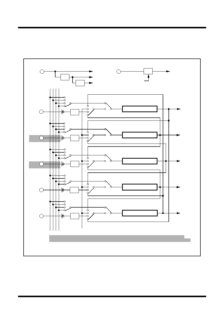
82
Tentative Specifications REV.A
Mitsubishi microcomputers
M16C / 62T Group
SINGLE-CHIP 16-BIT CMOS MICROCOMPUTER
S
pecifications in this manual are tentative and subject to change.
Under
development
Timer
Timer
There are eleven 16-bit timers. These timers can be classified by function into timers A (five) and timers B
(six). All these timers function independently. Figures 1.17.1 and 1.17.2 show the block diagram of timers.
· Timer mode
· One-shot mode
· PWM mode
· Timer mode
· One-shot mode
· PWM mode
· Timer mode
· One-shot mode
· PWM mode
· Timer mode
· One-shot mode
· PWM mode
· Timer mode
· One-shot mode
· PWM mode
· Event counter mode
· Event counter mode
· Event counter mode
· Event counter mode
· Event counter mode
TA0
IN
TA1
IN
TA2
IN
TA3
IN
TA4
IN
Timer A0
Timer A1
Timer A2
Timer A3
Timer A4
f
1
f
8
f
32
f
C32
Timer A0 interrupt
Timer A1 interrupt
Timer A2 interrupt
Timer A3 interrupt
Timer A4 interrupt
Noise
filter
Noise
filter
Noise
filter
Noise
filter
Noise
filter
1/32
f
C32
1/8
1/4
f
1
f
8
f
32
X
IN
X
CIN
Clock prescaler reset flag (bit 7
at address 0381
16
) set to "1"
Reset
Clock prescaler
Timer B2 overflow
Note 1: In M30623(80-pin package), do not use TA1
IN
and TA2
IN
as the event input, because these are not
connected to the external pin. And these pins have to do connection of unused pins (refer to Page 170).
Note 2: The TA0
IN
pin (P7
1
) is shared with RxD
2
and the TB5
IN
pin.
Figure 1.17.1. Timer A block diagram
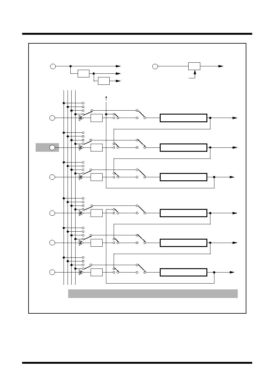
83
Tentative Specifications REV.A
Mitsubishi microcomputers
M16C / 62T Group
SINGLE-CHIP 16-BIT CMOS MICROCOMPUTER
S
pecifications in this manual are tentative and subject to change.
Under
development
Timer
Figure 1.17.2. Timer B block diagram
· Event counter mode
· Event counter mode
· Event counter mode
· Timer mode
· Pulse width measuring mode
· Timer mode
· Pulse width measuring mode
· Timer mode
· Pulse width measuring mode
TB0
IN
TB1
IN
TB2
IN
Timer B0
Timer B1
Timer B2
f
1
f
8
f
32
f
C32
Timer B0 interrupt
Noise
filter
Noise
filter
Noise
filter
1/32
f
C32
1/8
1/4
f
1
f
8
f
32
X
IN
X
CIN
Clock prescaler reset flag (bit 7
at address 0381
16
) set to "1"
Reset
Clock prescaler
Timer A
· Event counter mode
· Event counter mode
· Event counter mode
· Timer mode
· Pulse width measuring mode
· Timer mode
· Pulse width measuring mode
· Timer mode
· Pulse width measuring mode
TB3
IN
TB4
IN
TB5
IN
Timer B3
Timer B4
Timer B5
Timer B3 interrupt
Noise
filter
Noise
filter
Noise
filter
Timer B1 interrupt
Timer B2 interrupt
Timer B4 interrupt
Timer B5 interrupt
Note 1: In M30623(80-pin package), do not use TB1
IN
as the event input, because it is not connected
to the external pin. And these pins have to do connection of unused pins (refer to Page 170).
Note 2: The TB5
IN
pin (P7
1
) is shared with RxD
2
and the TA0
IN
pin.
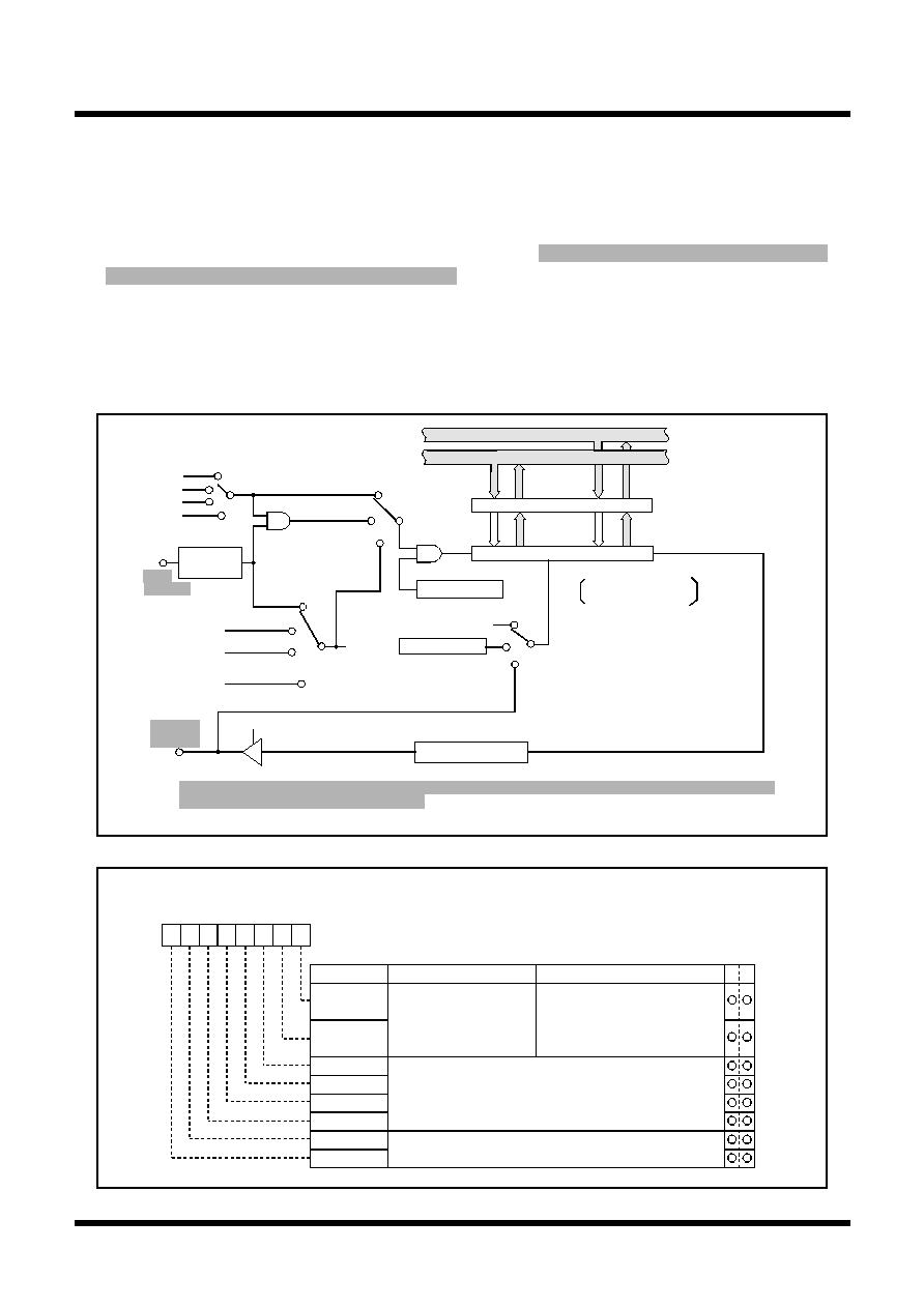
84
Tentative Specifications REV.A
Mitsubishi microcomputers
M16C / 62T Group
SINGLE-CHIP 16-BIT CMOS MICROCOMPUTER
S
pecifications in this manual are tentative and subject to change.
Under
development
Timer A
Timer A
Figure 1.17.3 shows the block diagram of timer A. Figures 1.17.4 to 1.17.6 show the timer A-related
registers.
Except in event counter mode, timers A0 through A4 all have the same function. Use the timer Ai mode
register (i = 0 to 4) bits 0 and 1 to choose the desired mode. But M30623(80-pin package), timer A1 and A2
have no I/O pin, so it operate as only internal timer.
Timer A has the four operation modes listed as follows:
· Timer mode: The timer counts an internal count source.
· Event counter mode: The timer counts pulses from an external source or a timer over flow.
· One-shot timer mode: The timer stops counting when the count reaches "0000
16
".
· Pulse width modulation (PWM) mode: The timer outputs pulses of a given width.
Figure 1.17.4. Timer A-related registers (1)
Count start flag
(Address 0380
16
)
Up count/down count
TAi
Addresses
TAj
TAk
Timer A0
0387
16
0386
16
Timer A4
Timer A1
Timer A1
0389
16
0388
16
Timer A0
Timer A2
Timer A2
038B
16
038A
16
Timer A1
Timer A3
Timer A3
038D
16
038C
16
Timer A2
Timer A4
Timer A4 038F
16
038E
16
Timer A3
Timer A0
Always down count except
in event counter mode
Reload register (16)
Counter (16)
Low-order
8 bits
High-order
8 bits
Clock source
selection
· Timer
(gate function)
· Timer
· One shot
· PWM
f
1
f
8
f
32
External
trigger
TAi
IN
(i = 0 to 4)
TB2 overflow
· Event counter
f
C32
Clock selection
TAj overflow
(j = i 1. Note, however, that j = 4 when i = 0)
Pulse output
Toggle flip-flop
TAi
OUT
(i = 0 to 4)
Data bus low-order bits
Data bus high-order bits
Up/down flag
Down count
(Address 0384
16
)
TAk overflow
(k = i + 1. Note, however, that k = 0 when i = 4)
Polarity
selection
Note 1: In M30623(80-pin package), do not select the function using TA1
IN
,
TA1
OUT
, or TA2
IN
, and
TA2
OUT
because
these are not connected to the external pin.
Note 2: The TA0
IN
pin (P7
1
) is shared with the TB5
IN
pin, RxD
2
, and SCL pin.
Timer Ai mode register
Symbol
Address
When reset
TAiMR(i=0 to 4)
0396
16
to 039A
16
00
16
Bit name
Function
Bit symbol
W
R
b7
b6
b5
b4
b3
b2
b1
b0
0 0 : Timer mode
0 1 : Event counter mode
1 0 : One-shot timer mode
1 1 : Pulse width modulation
(PWM) mode
b1 b0
TCK1
MR3
MR2
MR1
TMOD1
MR0
TMOD0
TCK0
Function varies with each operation mode
Count source select bit
(Function varies with each operation mode)
Operation mode select bit
Figure 1.17.3. Block diagram of timer A
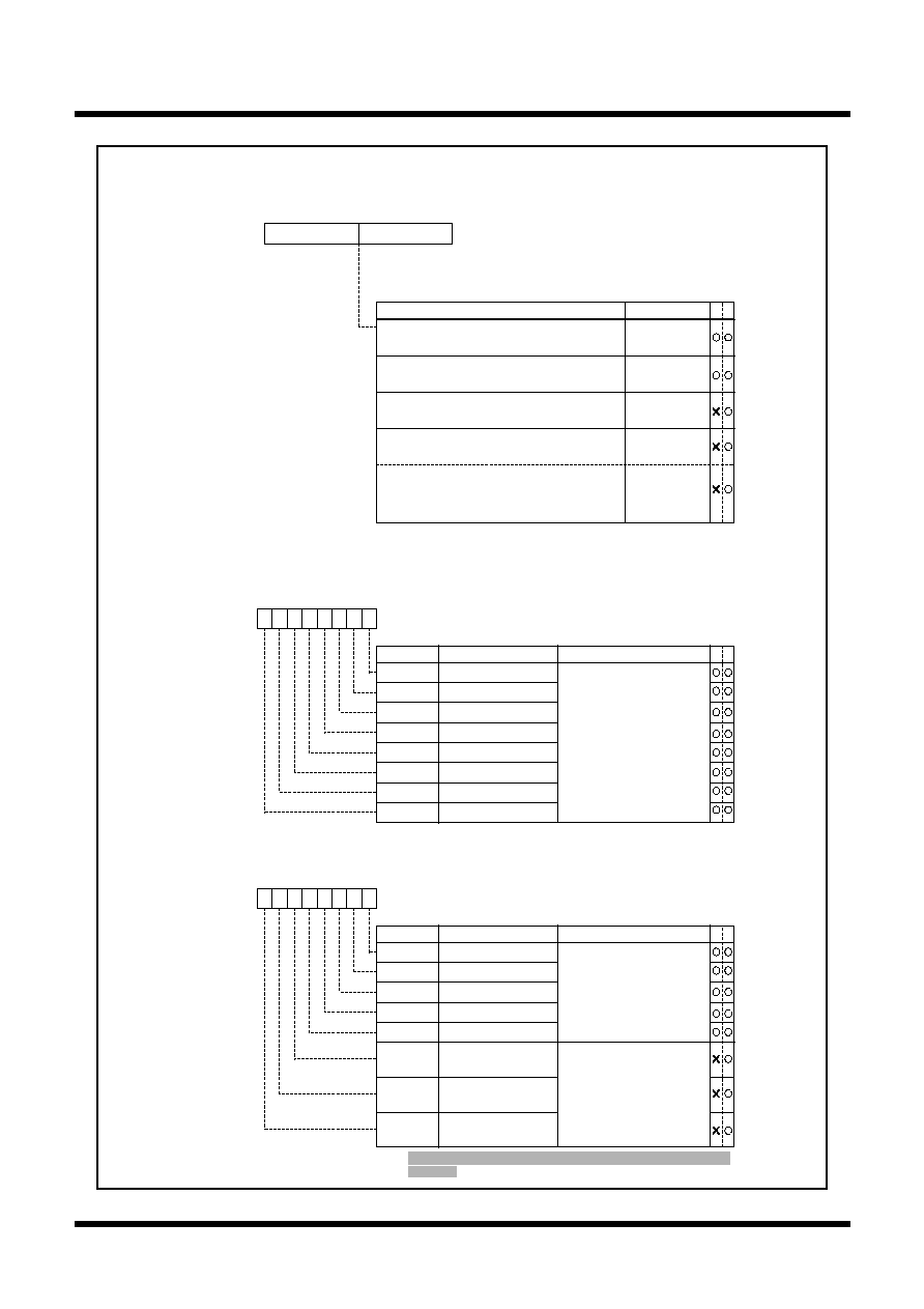
85
Tentative Specifications REV.A
Mitsubishi microcomputers
M16C / 62T Group
SINGLE-CHIP 16-BIT CMOS MICROCOMPUTER
S
pecifications in this manual are tentative and subject to change.
Under
development
Timer A
Figure 1.17.5. Timer A-related registers (2)
Timer A4 up/down flag
Timer A3 up/down flag
Timer A2 up/down flag
Timer A1 up/down flag
Timer A0 up/down flag
Timer A2 two-phase pulse
signal processing select bit
Timer A3 two-phase pulse
signal processing select bit
Timer A4 two-phase pulse
signal processing select bit
Symbol
Address
When reset
UDF
0384
16
00
16
TA4P
TA3P
TA2P
Up/down flag
Bit name
Function
Bit symbol
W
R
b7
b6
b5
b4
b3
b2
b1
b0
TA4UD
TA3UD
TA2UD
TA1UD
TA0UD
0 : Down count
1 : Up count
This specification becomes valid
when the up/down flag content is
selected for up/down switching
cause
0 : two-phase pulse signal
processing disabled
1 : two-phase pulse signal
processing enabled
When not using the two-phase
pulse signal processing function,
set the select bit to "0"
Symbol
Address
When reset
TABSR
0380
16
00
16
Count start flag
Bit name
Function
Bit symbol
W
R
b7
b6
b5
b4
b3
b2
b1
b0
Timer B2 count start flag
Timer B1 count start flag
Timer B0 count start flag
Timer A4 count start flag
Timer A3 count start flag
Timer A2 count start flag
Timer A1 count start flag
Timer A0 count start flag
0 : Stops counting
1 : Starts counting
TB2S
TB1S
TB0S
TA4S
TA3S
TA2S
TA1S
TA0S
Symbol
Address
When reset
TA0
0387
16
,0386
16
Indeterminate
TA1
0389
16
,0388
16
Indeterminate
TA2
038B
16
,038A
16
Indeterminate
TA3
038D
16
,038C
16
Indeterminate
TA4
038F
16
,038E
16
Indeterminate
b7
b0 b7
b0
(b15)
(b8)
Timer Ai register (Note)
W
R
· Timer mode
0000
16
to FFFF
16
Counts an internal count source
Function
Values that can be set
· Event counter mode
0000
16
to FFFF
16
Counts pulses from an external source or timer overflow
· One-shot timer mode
0000
16
to FFFF
16
Counts a one shot width
· Pulse width modulation mode (16-bit PWM)
Functions as a 16-bit pulse width modulator
· Pulse width modulation mode (8-bit PWM)
Timer low-order address functions as an 8-bit
prescaler and high-order address functions as an 8-bit
pulse width modulator
00
16
to FE
16
(Both high-order
and low-order
addresses)
0000
16
to FFFE
16
Note: Read and write data in 16-bit units.
Note 1: M30623(80-pin package) does not have I/O pins for TA2, so set this
bit to "0''.
(Note 1)
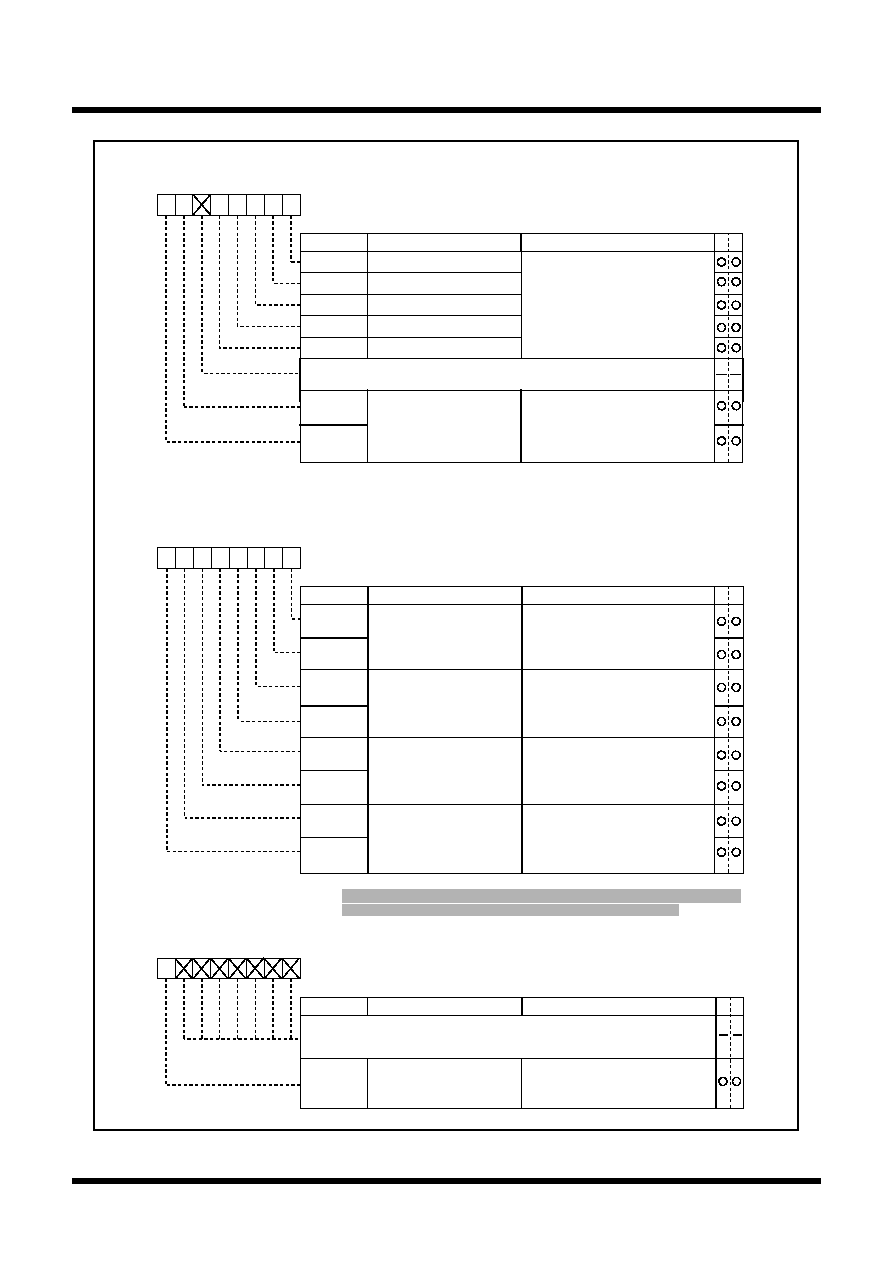
86
Tentative Specifications REV.A
Mitsubishi microcomputers
M16C / 62T Group
SINGLE-CHIP 16-BIT CMOS MICROCOMPUTER
S
pecifications in this manual are tentative and subject to change.
Under
development
Timer A
Symbol
Address
When reset
CPSRF
0381
16
0XXXXXXX
2
Clock prescaler reset flag
Bit name
Function
Bit symbol
b7
b6
b5
b4
b3
b2
b1
b0
Clock prescaler reset flag
0 : No effect
1 : Prescaler is reset
(When read, the value is "0")
CPSR
W
R
Nothing is assigned.
In an attempt to write to these bits, write "0". The value, if read, turns out to be
indeterminate.
TA1TGL
Symbol
Address
When reset
TRGSR
0383
16
00
16
Timer A1 event/trigger
select bit
0 0 :
Input on TA1
IN
is selected
(Note 1, 2)
0 1 : TB2 overflow is selected
1 0 : TA0 overflow is selected
1 1 : TA2 overflow is selected
Trigger select register
Bit name
Function
Bit symbol
b7
b6
b5
b4
b3
b2
b1
b0
0 0 :
Input on TA2
IN
is selected
(Note 1, 2)
0 1 : TB2 overflow is selected
1 0 : TA1 overflow is selected
1 1 : TA3 overflow is selected
0 0 :
Input on TA3
IN
is selected (Note 1)
0 1 : TB2 overflow is selected
1 0 : TA2 overflow is selected
1 1 : TA4 overflow is selected
0 0 :
Input on TA4
IN
is selected (Note 1)
0 1 : TB2 overflow is selected
1 0 : TA3 overflow is selected
1 1 : TA0 overflow is selected
Timer A2 event/trigger
select bit
Timer A3 event/trigger
select bit
Timer A4 event/trigger
select bit
W
R
TA1TGH
TA2TGL
TA2TGH
TA3TGL
TA3TGH
TA4TGL
TA4TGH
b1 b0
b3 b2
b5 b4
b7 b6
Note 1: Set the corresponding port direction register to "0".
Note 2: In M30623(80-pin package), do not select the function using TA1
IN
and
TA2
IN
,
because these are not connected to the external pin.
TA1OS
TA2OS
TA0OS
One-shot start flag
Symbol
Address
When reset
ONSF
0382
16
00X00000
2
Timer A0 one-shot start flag
Timer A1 one-shot start flag
Timer A2 one-shot start flag
Timer A3 one-shot start flag
Timer A4 one-shot start flag
TA3OS
TA4OS
Bit name
Function
Bit symbol
b7
b6
b5
b4
b3
b2
b1
b0
Nothing is assigned.
In an attempt to write to this bit, write "0". The value, if read, turns out to be indeterminate.
TA0TGL
TA0TGH
0 0 :
Input on TA0
IN
is selected (Note)
0 1 : TB2 overflow is selected
1 0 : TA4 overflow is selected
1 1 : TA1 overflow is selected
Timer A0 event/trigger
select bit
b7 b6
Note: Set the corresponding port direction register to "0".
W
R
1 : Timer start
When read, the value is "0"
Figure 1.17.6. Timer A-related registers (3)
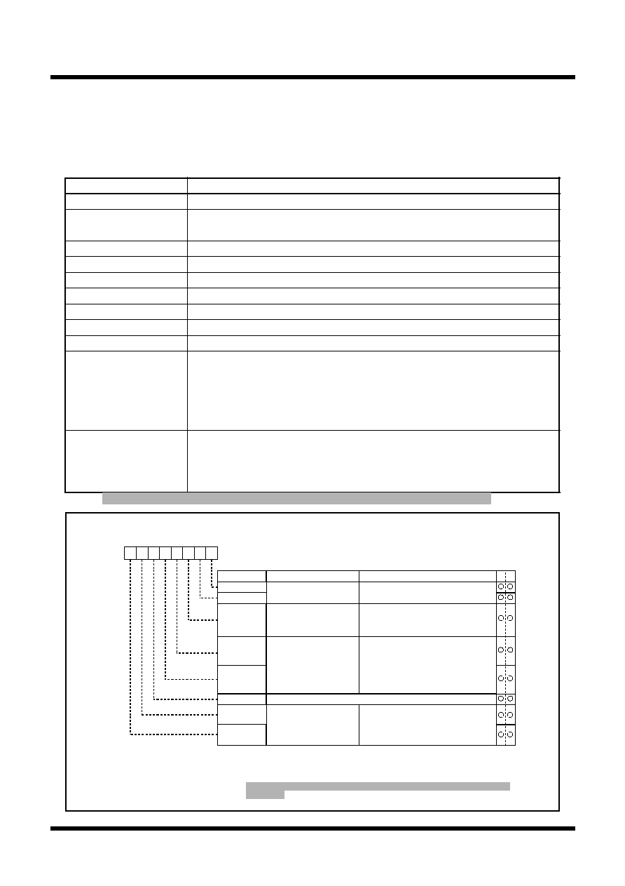
87
Tentative Specifications REV.A
Mitsubishi microcomputers
M16C / 62T Group
SINGLE-CHIP 16-BIT CMOS MICROCOMPUTER
S
pecifications in this manual are tentative and subject to change.
Under
development
Timer A
Item
Specification
Count source
f
1
, f
8
, f
32
, f
C32
Count operation
· Down count
· When the timer underflows, it reloads the reload register contents before continuing counting
Divide ratio
1/(n+1)
n : Set value
Count start condition
Count start flag is set (= 1)
Count stop condition
Count start flag is reset (= 0)
Interrupt request generation timing
When the timer underflows
TAi
IN
pin function
Programmable I/O port or gate input
TAi
OUT
pin function
Programmable I/O port or pulse output
Read from timer
Count value can be read out by reading timer Ai register
Write to timer
· When counting stopped
When a value is written to timer Ai register, it is written to both reload register and counter
· When counting in progress
When a value is written to timer Ai register, it is written to only reload register
(Transferred to counter at next reload time)
Select function
· Gate function
Counting can be started and stopped by the TAi
IN
pin's input signal
· Pulse output function
Each time the timer underflows, the TAi
OUT
pin's polarity is reversed
(1) Timer mode
In this mode, the timer counts an internally generated count source. (See Table 1.17.1.) Figure 1.17.7
shows the timer Ai mode register in timer mode.
Table 1.17.1. Specifications of timer mode
Note 1: The settings of the corresponding port register and port direction register
are invalid.
Note 2: The bit can be "0" or "1".
Note 3: Set the corresponding port direction register to "0".
Note 4: In timer A1 and A2 mode register of M30623(80-pin package), set these
bits to "0".
Timer Ai mode register
Symbol
Address
When reset
TAiMR(i=0 to 4)
0396
16
to 039A
16
00
16
Bit name
Function
Bit symbol
W
R
b7
b6
b5
b4
b3
b2
b1
b0
Operation mode
select bit
0 0 : Timer mode
b1 b0
TMOD1
TMOD0
MR0
Pulse output function
select bit
(Note 4)
0 : Pulse is not output
(TA
iOUT
pin is a normal port pin)
1 : Pulse is output (Note 1)
(TA
iOUT
pin is a pulse output pin)
Gate function select bit
0 X
(Note 2)
: Gate function not available
(TAi
IN
pin is a normal port pin)
1 0 : Timer counts only when TA
iIN
pin is
held "L" (Note 3)
1 1 : Timer counts only when TA
iIN
pin is
held "H" (Note 3)
b4 b3
MR2
MR1
MR3
0 (Must always be fixed to "0" in timer mode)
0 0 : f
1
0 1 : f
8
1 0 : f
32
1 1 : f
C32
b7 b6
TCK1
TCK0
Count source select bit
0
0
0
(Note 4)
Figure 1.17.7. Timer Ai mode register in timer mode
Note 1: M30623(80-pin package) does not have I/O pins(TAi
IN
,TAi
OUT
) for timer A1 and A2.
88
Tentative Specifications REV.A
Mitsubishi microcomputers
M16C / 62T Group
SINGLE-CHIP 16-BIT CMOS MICROCOMPUTER
S
pecifications in this manual are tentative and subject to change.
Under
development
Timer A
(2) Event counter mode
In this mode, the timer counts an external signal or an internal timer's overflow. Timers A0 and A1 can
count a single-phase external signal. Timers A2, A3, and A4 can count a single-phase and a two-phase
external signal. Table 1.17.2 lists timer specifications when counting a single-phase external signal.
Figure 1.17.8 shows the timer Ai mode register in event counter mode.
Table 1.17.3 lists timer specifications when counting a two-phase external signal. Figure 1.17.9 shows
the timer Ai mode register in event counter mode.
Figure 1.17.8. Timer Ai mode register in event counter mode
Timer Ai mode register
Note 1: In event counter mode, the count source is selected by the event / trigger select bit
(addresses 0382
16
and 0383
16
).
Note 2: The settings of the corresponding port register and port direction register are invalid.
Note 3: Valid only when counting an external signal.
Note 4: When an "L" signal is input to the TAi
OUT
pin, the downcount is activated. When "H",
the upcount is activated. Set the corresponding port direction register to "0".
Note 5: In Timer A1 and A2 mode register of M30623(80-pin package), set these bits to "0".
Symbol
Address
When reset
TAiMR(i = 0, 1)
0396
16
, 0397
16
00
16
W
R
b7
b6
b5
b4
b3
b2
b1
b0
Operation mode select bit
0 1 : Event counter mode
(Note 1)
b1 b0
TMOD0
MR0
Pulse output function
select bit (Note 5)
0 : Pulse is not output
(TA
iOUT
pin is a normal port pin)
1 : Pulse is output (Note 2)
(TA
iOUT
pin is a pulse output pin)
Count polarity
select bit (Note 3,Note 5)
MR2
MR1
MR3
0 (Must always be fixed to "0" in event counter mode)
TCK0
Count operation type
select bit
0
1
0
0 : Counts external signal's falling edge
1 : Counts external signal's rising edge
Up/down switching cause
select bit (Note 5)
0 : Up/down flag's content
1 : TA
iOUT
pin's input signal (Note 4)
0 : Reload type
1 : Free-run type
Bit symbol
Bit name
Function
R W
TCK1
Invalid in event counter mode
Can be "0" or "1"
TMOD1
Item
Specification
Count source
· External signals input to TAi
IN
pin (effective edge can be selected by software)
· TB2 overflow, TAj overflow
Count operation
· Up count or down count can be selected by external signal or software
· When the timer overflows or underflows, it reloads the reload register con
tents before continuing counting (Note)
Divide ratio
1/ (FFFF
16
- n + 1) for up count
1/ (n + 1) for down count
n : Set value
Count start condition
Count start flag is set (= 1)
Count stop condition
Count start flag is reset (= 0)
Interrupt request generation timing The timer overflows or underflows
TAi
IN
pin function
Programmable I/O port or count source input
TAi
OUT
pin function
Programmable I/O port, pulse output, or up/down count select input
Read from timer
Count value can be read out by reading timer Ai register
Write to timer
· When counting stopped
When a value is written to timer Ai register, it is written to both reload register and counter
· When counting in progress
When a value is written to timer Ai register, it is written to only reload register
(Transferred to counter at next reload time)
Select function
· Free-run count function
Even when the timer overflows or underflows, the reload register content is not reloaded to it
· Pulse output function
Each time the timer overflows or underflows, the TAi
OUT
pin's polarity is reversed
Note 1: This does not apply when the free-run function is selected.
Note 2: M30623(80-pin package) does not have I/O pins(TAi
IN
,TAi
OUT
) for timer A1 and A2.
Table 1.17.2. Timer specifications in event counter mode (when not processing two-phase pulse signal)
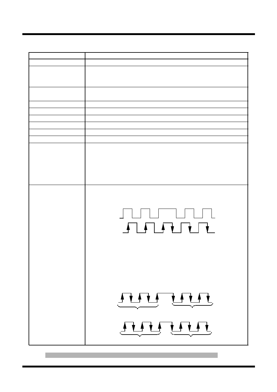
89
Tentative Specifications REV.A
Mitsubishi microcomputers
M16C / 62T Group
SINGLE-CHIP 16-BIT CMOS MICROCOMPUTER
S
pecifications in this manual are tentative and subject to change.
Under
development
Timer A
Item
Specification
Count source
· Two-phase pulse signals input to TAi
IN
or TAi
OUT
pin
Count operation
· Up count or down count can be selected by two-phase pulse signal
· When the timer overflows or underflows, the reload register content is
reloaded and the timer starts over again (Note)
Divide ratio
1/ (FFFF
16
-
n + 1) for up count
1/ (n + 1) for down count
n : Set value
Count start condition
Count start flag is set (= 1)
Count stop condition
Count start flag is reset (= 0)
Interrupt request generation timing
Timer overflows or underflows
TAi
IN
pin function
Two-phase pulse input
TAi
OUT
pin function
Two-phase pulse input
Read from timer
Count value can be read out by reading timer A2, A3, or A4 register
Write to timer
· When counting stopped
When a value is written to timer A2, A3, or A4 register, it is written to both
reload register and counter
· When counting in progress
When a value is written to timer A2, A3, or A4 register, it is written to only
reload register. (Transferred to counter at next reload time.)
Select function
· Normal processing operation
The timer counts up rising edges or counts down falling edges on the TAi
IN
pin when input signal on the TAi
OUT
pin is "H"
· Multiply-by-4 processing operation
If the phase relationship is such that the TAi
IN
pin goes "H" when the input
signal on the TAi
OUT
pin is "H", the timer counts up rising and falling edges
on the TAi
OUT
and TAi
IN
pins. If the phase relationship is such that the
TAi
IN
pin goes "L" when the input signal on the TAi
OUT
pin is "H", the timer
counts down rising and falling edges on the TAi
OUT
and TAi
IN
pins.
Note 1: This does not apply when the free-run function is selected.
Note 2: M30623(80-pin package) does not have I/O pins(TAi
IN
,TAi
OUT
) for timer A1 and A2.
Table 1.17.3. Timer specifications in event counter mode (when processing two-phase pulse signal with timers A2, A3, and A4)
TAi
OUT
Up
count
Up
count
Up
count
Down
count
Down
count
Down
count
TAi
IN
(i=2,3)
TAi
OUT
TAi
IN
(i=3,4)
Count up all edges
Count up all edges
Count down all edges
Count down all edges
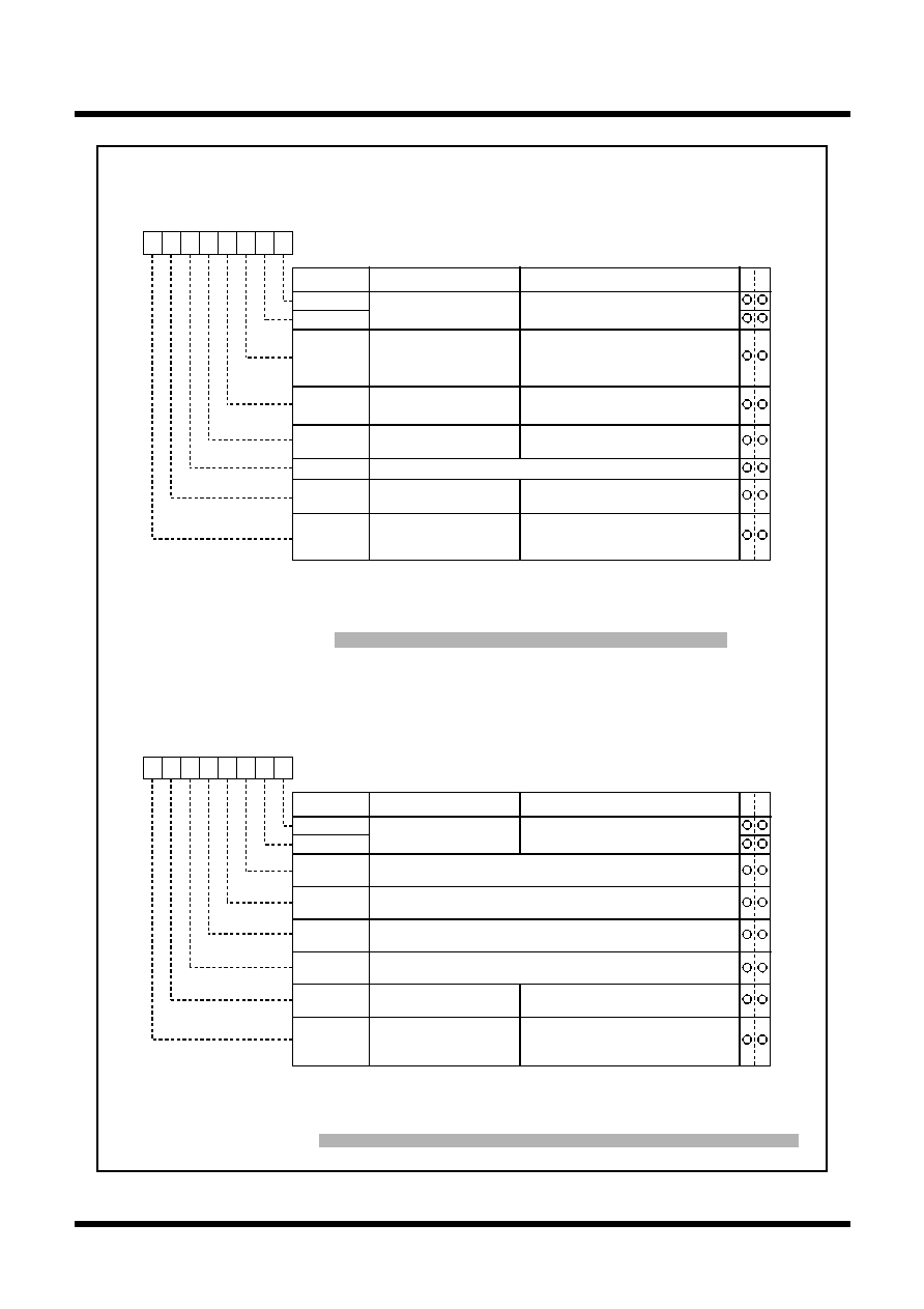
90
Tentative Specifications REV.A
Mitsubishi microcomputers
M16C / 62T Group
SINGLE-CHIP 16-BIT CMOS MICROCOMPUTER
S
pecifications in this manual are tentative and subject to change.
Under
development
Timer A
Note 1: The settings of the corresponding port register and port direction register are invalid.
Note 2: This bit is valid when only counting an external signal.
Note 3: Set the corresponding port direction register to "0".
Note 4: This bit is valid for the timer A3 mode register.
For timer A2 and A4 mode registers, this bit can be "0 "or "1".
Note 5: Set these bits to "0", in timer A2 mode register of M30623(80-pin package).
Timer Ai mode register
(When not using two-phase pulse signal processing)
Symbol
Address
When reset
TAiMR(i = 2 to 4) 0398
16
to 039A
16
00
16
b7
b6
b5
b4
b3
b2
b1
b0
Operation mode select bit
0 1 : Event counter mode
b1 b0
TMOD1
TMOD0
MR0
Pulse output function
select bit (Note 5)
0 : Pulse is not output
(TAi
OUT
pin is a normal port pin)
1 : Pulse is output (Note 1)
(TAi
OUT
pin is a pulse output pin)
Count polarity select bit
(Note 2,Note 5)
MR2
MR1
MR3
0 : (Must always be "0" in event counter mode)
TCK1
TCK0
0 1
0
0 : Counts external signal's falling edges
1 : Counts external signal's rising edges
Up/down switching cause
select bit (Note 5)
0 : Up/down flag's content
1 : TA
iOUT
pin's input signal (Note 3)
Bit symbol
Bit name
Function
W
R
Count operation type
select bit
Two-phase pulse signal
processing operation
select bit (Note 4)
0 : Reload type
1 : Free-run type
0 : Normal processing operation
1 : Multiply-by-4 processing operation
Note 1: This bit is valid for timer A3 mode register.
For timer A2 and A4 mode registers, this bit can be "0" or "1".
Note 2: When performing two-phase pulse signal processing, make sure the two-phase pulse
signal processing operation select bit (address 0384
16
) is set to "1". Also, always be
sure to set the event/trigger select bit (addresses 0382
16
and 0383
16
) to "00".
Note 3: In M30623(80-pin package), do not use timer A2 for the two-phase pulse signal processing.
Timer Ai mode register
(When using two-phase pulse signal processing)
Symbol
Address
When reset
TAiMR(i = 2 to 4) 0398
16
to 039A
16
00
16
b7
b6
b5
b4
b3
b2
b1
b0
Operation mode select bit
0 1 : Event counter mode
b1 b0
TMOD1
TMOD0
MR0
0 (Must always be "0" when using two-phase pulse signal
processing)
0 (Must always be "0" when using two-phase pulse signal
processing)
MR2
MR1
MR3
0 (Must always be "0" when using two-phase pulse signal
processing)
TCK1
TCK0
0 1
0
1 (Must always be "1" when using two-phase pulse signal
processing)
Bit symbol
Bit name
Function
W
R
Count operation type
select bit
Two-phase pulse
processing operation
select bit (Note 1)(Note 2)
0 : Reload type
1 : Free-run type
0 : Normal processing operation
1 : Multiply-by-4 processing operation
0
0
1
Figure 1.17.9. Timer Ai mode register in event counter mode
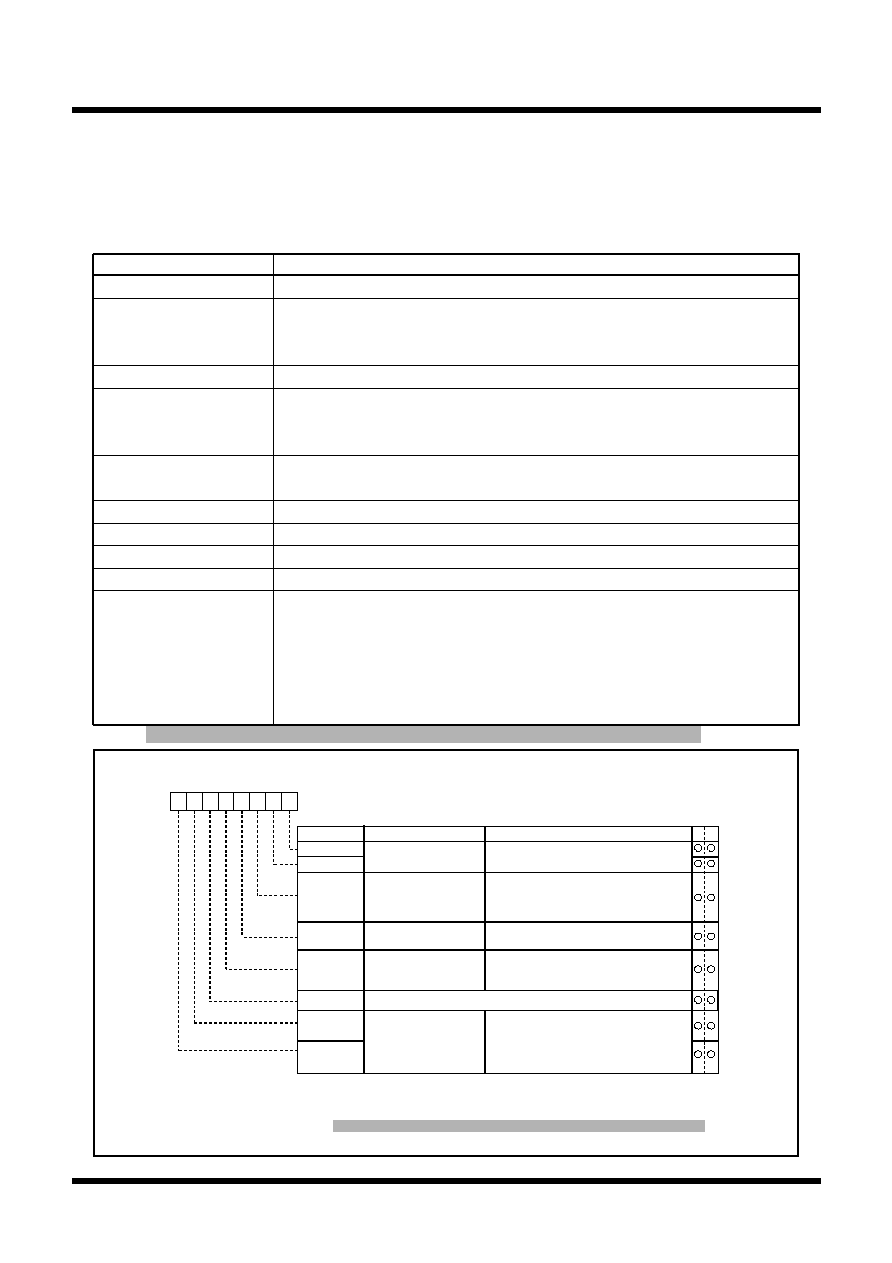
91
Tentative Specifications REV.A
Mitsubishi microcomputers
M16C / 62T Group
SINGLE-CHIP 16-BIT CMOS MICROCOMPUTER
S
pecifications in this manual are tentative and subject to change.
Under
development
Timer A
Item
Specification
Count source
f
1
, f
8
, f
32
, f
C32
Count operation
· The timer counts down
· When the count reaches 0000
16
, the timer stops counting after reloading a new count
· If a trigger occurs when counting, the timer reloads a new count and restarts counting
Divide ratio
1/n n : Set value
Count start condition
· An external trigger is input
· The timer overflows
· The one-shot start flag is set (= 1)
Count stop condition
· A new count is reloaded after the count has reached 0000
16
· The count start flag is reset (= 0)
Interrupt request generation timing
The count reaches 0000
16
TAi
IN
pin function
Programmable I/O port or trigger input
TAi
OUT
pin function
Programmable I/O port or pulse output
Read from timer
When timer Ai register is read, it indicates an indeterminate value
Write to timer
· When counting stopped
When a value is written to timer Ai register, it is written to both reload
register and counter
· When counting in progress
When a value is written to timer Ai register, it is written to only reload register
(Transferred to counter at next reload time)
Table1.17.4. Timer specifications in one-shot timer mode
Figure 1.17.10. Timer Ai mode register in one-shot timer mode
(3) One-shot timer mode
In this mode, the timer operates only once. (See Table 1.17.4.) When a trigger occurs, the timer starts up
and continues operating for a given period. Figure 1.17.10 shows the timer Ai mode register in one-shot
timer mode.
Bit name
Timer Ai mode register
Symbol
Address
When reset
TAiMR(i = 0 to 4) 0396
16
to 039A
16
00
16
Function
Bit symbol
b7
b6
b5
b4
b3
b2
b1
b0
Operation mode select bit
1 0 : One-shot timer mode
b1 b0
TMOD1
TMOD0
MR0
Pulse output function
select bit (Note 4)
0 : Pulse is not output
(TA
iOUT
pin is a normal port pin)
1 : Pulse is output (Note 1)
(TAi
OUT
pin is a pulse output pin)
MR2
MR1
MR3
0 (Must always be "0" in one-shot timer mode)
0 0 : f
1
0 1 : f
8
1 0 : f
32
1 1 : f
C32
b7 b6
TCK1
TCK0
Count source select bit
1 0
0
0 : One-shot start flag is valid
1 : Selected by event/trigger select
register
Trigger select bit
External trigger select
bit (Note 2) (Note 4)
0 : Falling edge of TAi
IN
pin's input signal (Note 3)
1 : Rising edge of TAi
IN
pin's input signal (Note 3)
Note 1: The settings of the corresponding port register and port direction register are invalid.
Note 2: Valid only when the TA
iIN
pin is selected by the event/trigger select bit
(addresses 0382
16
and 0383
16
). If timer overflow is selected, this bit can be "1" or "0".
Note 3: Set the corresponding port direction register to "0".
Note 4: Set these bits to "0", in timer A1 and A2 mode register of M30623(80-pin package).
W
R
Note 1: M30623(80-pin package) does not have I/O pins(TAi
IN
,TAi
OUT
) for timer A1 and A2.
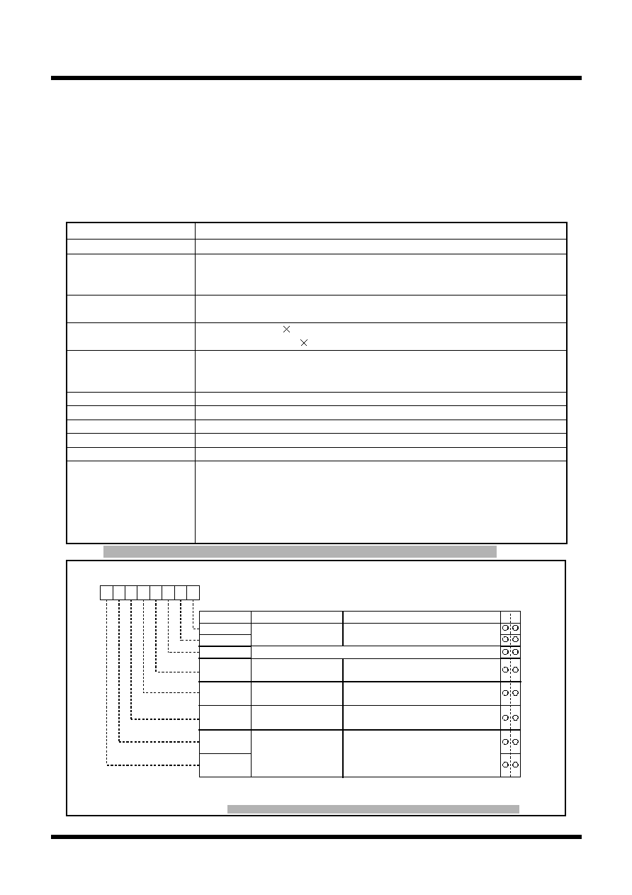
92
Tentative Specifications REV.A
Mitsubishi microcomputers
M16C / 62T Group
SINGLE-CHIP 16-BIT CMOS MICROCOMPUTER
S
pecifications in this manual are tentative and subject to change.
Under
development
Timer A
(4) Pulse width modulation (PWM) mode
In this mode, the timer outputs pulses of a given width in succession. (See Table 1.17.5.) In this mode, the
counter functions as either a 16-bit pulse width modulator or an 8-bit pulse width modulator. Figure
1.17.11 shows the timer Ai mode register in pulse width modulation mode. Figure 1.17.12 shows the
example of how a 16-bit pulse width modulator operates. Figure 1.17.13 shows the example of how an 8-
bit pulse width modulator operates.
Figure 1.17.11. Timer Ai mode register in pulse width modulation mode
Table 1.17.5. Timer specifications in pulse width modulation mode
Bit name
Timer Ai mode register
Symbol
Address
When reset
TAiMR(i=0 to 4)
0396
16
to 039A
16
00
16
Function
Bit symbol
b7
b6
b5
b4
b3
b2
b1
b0
Operation mode
select bit
1 1 : PWM mode
b1 b0
TMOD1
TMOD0
MR0
MR2
MR1
MR3
0 0 : f
1
0 1 : f
8
1 0 : f
32
1 1 : f
C32
b7 b6
TCK1
TCK0
Count source select bit
W
R
1
1
1
1 (Must always be "1" in PWM mode) (Note 3)
16/8-bit PWM mode
select bit
0: Functions as a 16-bit pulse width modulator
1: Functions as an 8-bit pulse width modulator
Trigger select bit
External trigger select
bit (Note 1) (Note 3)
0: Falling edge of TAi
IN
pin's input signal (Note 2)
1: Rising edge of TAi
IN
pin's input signal (Note 2)
0: Count start flag is valid
1: Selected by event/trigger select register
Note 1: Valid only when the TA
iIN
pin is selected by the event/trigger select bit
(addresses 0382
16
and 0383
16
). If timer overflow is selected, this bit can be "1" or "0".
Note 2: Set the corresponding port direction register to "0".
Note 3: Set these bits to "0", in timer A1 and A2 mode register of M30623(80-pin package).
Item
Specification
Count source
f
1
, f
8
, f
32
, f
C32
Count operation
· The timer counts down (operating as an 8-bit or a 16-bit pulse width modulator)
· The timer reloads a new count at a rising edge of PWM pulse and continues counting
· The timer is not affected by a trigger that occurs when counting
16-bit PWM
· High level width
n / fi n : Set value
· Cycle time
(2
16
-1) / fi fixed
8-bit PWM
· High level width n (m+1) / fi
n : values set to timer Ai register's high-order address
· Cycle time
(2
8
-1) (m+1) / fi
m : values set to timer Ai register's low-order address
Count start condition
· External trigger is input
· The timer overflows
· The count start flag is set (= 1)
Count stop condition
· The count start flag is reset (= 0)
Interrupt request generation timing
PWM pulse goes "L"
TAi
IN
pin function
Programmable I/O port or trigger input
TAi
OUT
pin function
Pulse output
Read from timer
When timer Ai register is read, it indicates an indeterminate value
Write to timer
· When counting stopped
When a value is written to timer Ai register, it is written to both reload
register and counter
· When counting in progress
When a value is written to timer Ai register, it is written to only reload register
(Transferred to counter at next reload time)
Note 1: M30623(80-pin package) does not have I/O pins(TAi
IN
,TAi
OUT
) for timer A1 and A2.
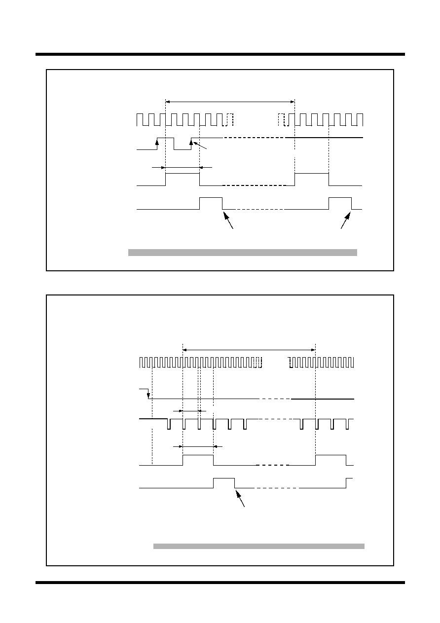
93
Tentative Specifications REV.A
Mitsubishi microcomputers
M16C / 62T Group
SINGLE-CHIP 16-BIT CMOS MICROCOMPUTER
S
pecifications in this manual are tentative and subject to change.
Under
development
Timer A
1 / f
i
X
(2 1)
16
Count source
TA
iIN
pin
input signal
PWM pulse output
from TA
iOUT
pin
Condition : Reload register = 0003
16
, when external trigger
(rising edge of TA
iIN
pin input signal) is selected
Trigger is not generated by this signal
"H"
"H"
"L"
"L"
Timer Ai interrupt
request bit
"1"
"0"
Cleared to "0" when interrupt request is accepted, or cleared by software
f
i
: Frequency of count source
(f
1
, f
8
, f
32
, f
C32
)
Note 1: M30623(80-pin package) does not have I/O pins(TAiIN,TAiOUT) for timer A1 and A2.
Note 2: n = 0000
16
to FFFE
16
.
1 / f
i
X
n
Count source (Note1)
TA
iIN
pin input signal
Underflow signal of
8-bit prescaler (Note2)
PWM pulse output
from TA
iOUT
pin(Note 3)
"H"
"H"
"H"
"L"
"L"
"L"
"1"
"0"
Timer Ai interrupt
request bit
Cleared to "0" when interrupt request is accepted, or cleaerd by software
f
i
: Frequency of count source
(f
1
, f
8
, f
32
, f
C32
)
Note 1: The 8-bit prescaler counts the count source.
Note 2: The 8-bit pulse width modulator counts the 8-bit prescaler's underflow signal.
Note 3: M30623(80-pin package) does not have no I/O pins(TAiIN,TAiOUT) for timer A1 and A2.
Note 4: m = 00
16
to FE
16
; n = 00
16
to FE
16
.
Condition : Reload register high-order 8 bits = 02
16
Reload register low-order 8 bits = 02
16
External trigger (falling edge of TA
iIN
pin input signal) is selected
1 / f
i
X (m
+ 1) X (2 1)
8
1 / f
i
X (m + 1) X n
1 / f
i
X (m + 1)
(Note 3)
Figure 1.17.12. Example of how a 16-bit pulse width modulator operates
Figure 1.17.13. Example of how an 8-bit pulse width modulator operates
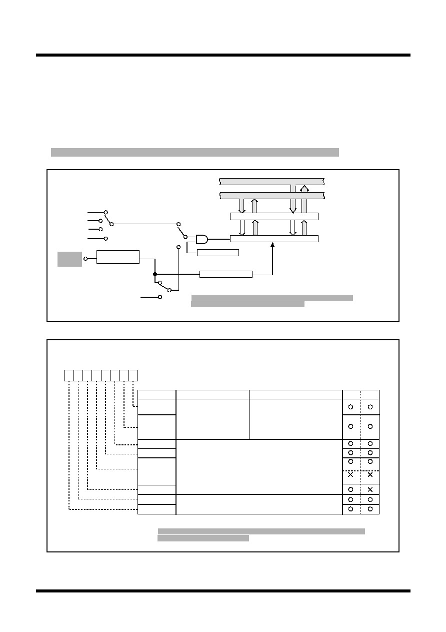
94
Tentative Specifications REV.A
Mitsubishi microcomputers
M16C / 62T Group
SINGLE-CHIP 16-BIT CMOS MICROCOMPUTER
S
pecifications in this manual are tentative and subject to change.
Under
development
Timer B
Timer B
Figure 1.17.14 shows the block diagram of timer B. Figures 1.17.15 and 1.17.16 show the timer B-related
registers.
Use the timer Bi mode register (i = 0 to 2) bits 0 and 1 to choose the desired mode.
Timer B has three operation modes listed as follows:
Figure 1.17.15. Timer B-related registers (1)
Timer Bi mode register
Symbol
Address
When reset
TBiMR(i = 0 to 5) 039B
16
to 039D
16
00XX0000
2
035B
16
to 035D
16
00XX0000
2
Bit name
Function
Bit symbol
W
R
b7
b6
b5
b4
b3
b2
b1
b0
0 0 : Timer mode
0 1 : Event counter mode
1 0 : Pulse period/pulse width
measurement mode (Note 3)
1 1 : Inhibited
b1 b0
TCK1
MR3
MR2
MR1
TMOD1
MR0
TMOD0
TCK0
Function varies with each operation mode
Count source select bit
(Function varies with each operation mode)
Operation mode select bit
(Note 1)
(Note 2)
Note 1: Timer B0, timer B3.
Note 2: Timer B1, timer B2, timer B4, timer B5.
Note 3: In the timer B1 mode register of M30623(80-pin package), do not use this mode,
because timer B1 has no input pin.
Clock source selection
(address 0380
16
)
· Event counter
· Timer
· Pulse period/pulse width measurement
Reload register (16)
Low-order 8 bits
High-order 8 bits
Data bus low-order bits
Data bus high-order bits
f
1
f
8
f
32
TBj overflow
(j = i 1. Note, however,
j = 2 when i = 0,
j = 5 when i = 3)
Can be selected in only
event counter mode
Count start flag
f
C32
Polarity switching
and edge pulse
TBi
IN
(i = 0 to 5)
Counter reset circuit
Counter (16)
TBi Address
TBj
Timer B0 0391
16
0390
16
Timer B2
Timer B1 0393
16
0392
16
Timer B0
Timer B2 0395
16
0394
16
Timer B1
Timer B3 0351
16
0350
16
Timer B5
Timer B4 0353
16
0352
16
Timer B3
Timer B5 0355
16
0354
16
Timer B4
Note 1: In M30623(80-pin package), do not select the function using TB1
IN
,
because it is not connected to the external pin.
Note 2: The TB5
IN
pin is shared with the TA0
IN
pin, RxD
2
, and SCL pin.
· Timer mode: The timer counts an internal count source.
· Event counter mode: The timer counts pulses from an external source or a timer overflow.
· Pulse period/pulse width measuring mode: The timer measures an external signal's pulse period or pulse width.
Figure 1.17.14. Block diagram of timer B
But, M30623(80-pin package), timer B1 has no input pin, so funcs as the internal timer.
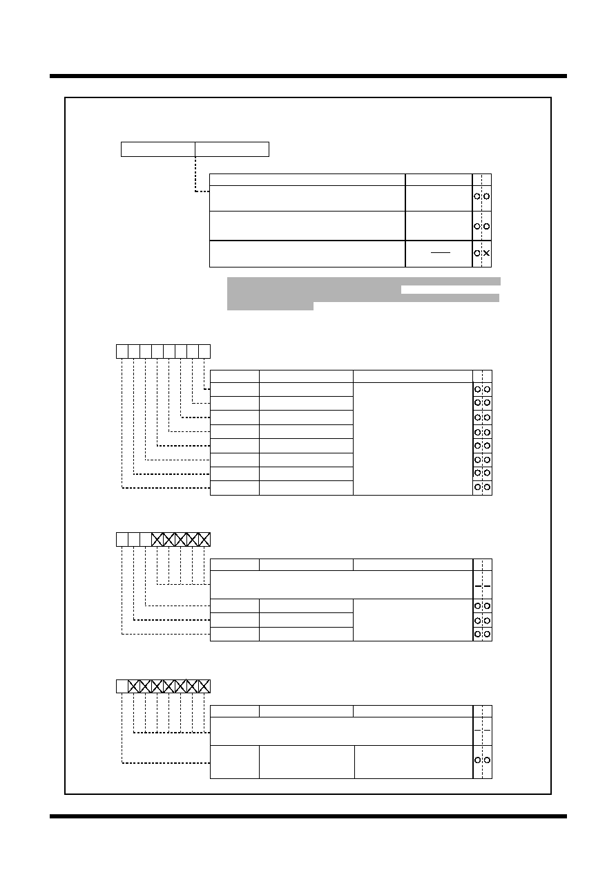
95
Tentative Specifications REV.A
Mitsubishi microcomputers
M16C / 62T Group
SINGLE-CHIP 16-BIT CMOS MICROCOMPUTER
S
pecifications in this manual are tentative and subject to change.
Under
development
Timer B
Note 1: Read and write data in 16-bit units.
Note 2: In the timer B1 of M30623(80-pin package), do not select the external pulses input
as count source, because timer B1 has no input pin.
Note 3: In the timer B1 of M30623(80-pin package), this mode does not function, because
timer B1 has no input pin.
Symbol
Address
When reset
TABSR
0380
16
00
16
Count start flag
Bit name
Bit symbol
W
R
b7
b6
b5
b4
b3
b2
b1
b0
Timer B2 count start flag
Timer B1 count start flag
Timer B0 count start flag
Timer A4 count start flag
Timer A3 count start flag
Timer A2 count start flag
Timer A1 count start flag
Timer A0 count start flag
0 : Stops counting
1 : Starts counting
TB2S
TB1S
TB0S
TA4S
TA3S
TA2S
TA1S
TA0S
Function
Symbol
Address
When reset
CPSRF
0381
16
0XXXXXXX
2
Clock prescaler reset flag
Bit name
Function
Bit symbol
W
R
b7
b6
b5
b4
b3
b2
b1
b0
Clock prescaler reset flag
0 : No effect
1 : Prescaler is reset
(When read, the value is "0")
CPSR
Symbol
Address
When reset
TB0
0391
16
, 0390
16
Indeterminate
TB1
0393
16
, 0392
16
Indeterminate
TB2
0395
16
, 0394
16
Indeterminate
TB3
0351
16
, 0350
16
Indeterminate
TB4
0353
16
, 0352
16
Indeterminate
TB5
0355
16
, 0354
16
Indeterminate
b7
b0 b7
b0
(b15)
(b8)
Timer Bi register (Note)
W
R
· Pulse period / pulse width measurement mode
Measures a pulse period or width
· Timer mode
0000
16
to FFFF
16
Counts the timer's period
Function
Values that can be set
· Event counter mode
0000
16
to FFFF
16
Counts external pulses input or a timer overflow
Symbol
Address
When reset
TBSR
0340
16
00
16
Timer B3, 4, 5 count start flag
Bit name
Bit symbol
W
R
b7
b6
b5
b4
b3
b2
b1
b0
Timer B5 count start flag
Timer B4 count start flag
Timer B3 count start flag
0 : Stops counting
1 : Starts counting
TB5S
TB4S
TB3S
Nothing is assigned.
In an attempt to write to these bits, write "0". The value, if read, turns
out to be "0".
Function
Nothing is assigned.
In an attempt to write to these bits, write "0". The value, if read, turns
out to be "0".
(Note 3)
(Note 2)
Figure 1.17.16. Timer B-related registers (2)
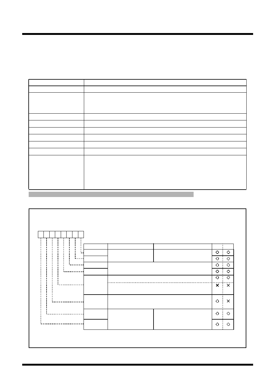
96
Tentative Specifications REV.A
Mitsubishi microcomputers
M16C / 62T Group
SINGLE-CHIP 16-BIT CMOS MICROCOMPUTER
S
pecifications in this manual are tentative and subject to change.
Under
development
Timer B
Count source
f
1
, f
8
, f
32
, f
C32
Count operation
· Counts down
· When the timer underflows, it reloads the reload register contents before
continuing counting
Divide ratio
1/(n+1)
n : Set value
Count start condition
Count start flag is set (= 1)
Count stop condition
Count start flag is reset (= 0)
Interrupt request generation timing
The timer underflows
TBi
IN
pin function
Programmable I/O port
Read from timer
Count value is read out by reading timer Bi register
Write to timer
· When counting stopped
When a value is written to timer Bi register, it is written to both reload register and counter
· When counting in progress
When a value is written to timer Bi register, it is written to only reload register
(Transferred to counter at next reload time)
Note 1: Timer B0, timer B3.
Note 2: Timer B1, timer B2, timer B4, timer B5.
Timer Bi mode register
Symbol
Address
When reset
TBiMR(i=0 to 5)
039B
16
to 039D
16
00XX0000
2
035B
16
to 035D
16
00XX0000
2
Bit name
Function
Bit symbol
W
R
b7
b6
b5
b4
b3
b2
b1
b0
Operation mode select bit
0 0 : Timer mode
b1 b0
TMOD1
TMOD0
MR0
Invalid in timer mode
Can be "0" or "1"
MR2
MR1
MR3
0 0 : f
1
0 1 : f
8
1 0 : f
32
1 1 : f
C32
TCK1
TCK0
Count source select bit
0
Invalid in timer mode.
In an attempt to write to this bit, write "0". The value, if read in
timer mode, turns out to be indeterminate.
0
0 (Fixed to "0" in timer mode ; i = 0, 3)
Nothing is assiigned (i = 1, 2, 4, 5).
In an attempt to write to this bit, write "0". The value, if read, turns out
to be indeterminate.
(Note 1)
(Note 2)
b7 b6
Note 1: M30623(80-pin package) does not have the input pin(TB1
IN
) of timer B1.
(1) Timer mode
In this mode, the timer counts an internally generated count source. (See Table 1.17.6.) Figure 1.17.17
shows the timer Bi mode register in timer mode.
Figure 1.17.17. Timer Bi mode register in timer mode
Table 1.17.6. Timer specifications in timer mode
Item
Specification
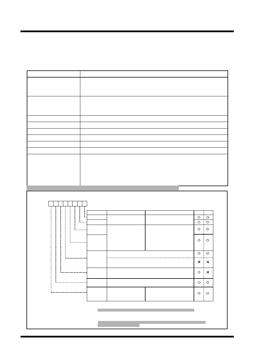
97
Tentative Specifications REV.A
Mitsubishi microcomputers
M16C / 62T Group
SINGLE-CHIP 16-BIT CMOS MICROCOMPUTER
S
pecifications in this manual are tentative and subject to change.
Under
development
Timer B
Item
Specification
Count source
· External signals input to TBi
IN
pin
· Effective edge of count source can be a rising edge, a falling edge, or falling
and rising edges as selected by software
Count operation
· Counts down
· When the timer underflows, it reloads the reload register contents before
continuing counting
Divide ratio
1/(n+1)
n : Set value
Count start condition
Count start flag is set (= 1)
Count stop condition
Count start flag is reset (= 0)
Interrupt request generation timing The timer underflows
TBi
IN
pin function
Count source input
Read from timer
Count value can be read out by reading timer Bi register
Write to timer
· When counting stopped
When a value is written to timer Bi register, it is written to both reload register and counter
· When counting in progress
When a value is written to timer Bi register, it is written to only reload register
(Transferred to counter at next reload time)
(2) Event counter mode
In this mode, the timer counts an external signal or an internal timer's overflow. (See Table 1.17.7.)
Figure 1.17.18 shows the timer Bi mode register in event counter mode.
Table 1.17.7. Timer specifications in event counter mode
Figure 1.17.18. Timer Bi mode register in event counter mode
Timer Bi mode register
Symbol
Address
When reset
TBiMR(i=0 to 5)
039B
16
to 039D
16
00XX0000
2
035B
16
to 035D
16
00XX0000
2
Bit name
Function
Bit symbol
W
R
b7
b6
b5
b4
b3
b2
b1
b0
Operation mode select bit
0 1 : Event counter mode
b1 b0
TMOD1
TMOD0
MR0
Count polarity select
bit
(Note 1)
MR2
MR1
MR3
Invalid in event counter mode.
In an attempt to write to this bit, write "0". The value, if read in
event counter mode, turns out to be indeterminate.
TCK1
TCK0
0
1
0 0 : Counts external signal's
falling edges
0 1 : Counts external signal's
rising edges
1 0 : Counts external signal's
falling and rising edges
1 1 : Inhibited
b3 b2
Nothing is assigned (i = 1, 2, 4, 5).
In an attempt to write to this bit, write "0". The value, if read,
turns out to be indeterminate.
Note 1: Valid only when input from the TBi
IN
pin is selected as the event clock.
If timer's overflow is selected, this bit can be "0" or "1".
In timer B1 mode register of M30623(80-pin package), this bit is invalid.
Note 2: Timer B0, timer B3.
Note 3: Timer B1, timer B2, timer B4, timer B5.
Note 4: Set the corresponding port direction register to "0".
In M30623(80-pin package), do not use the input from TB1
IN
pin as event clock,
because there is no TB1
IN
pin.
Invalid in event counter mode.
Can be "0" or "1".
Event clock select
0 : Input from TBi
IN
pin (Note 4)
1 : TBj overflow
(j = i 1; however, j = 2 when i = 0,
j = 5 when i = 3)
0 (Fixed to "0" in event counter mode; i = 0, 3)
(Note 2)
(Note 3)
Note 1: M30623(80-pin package) does not have the input pin(TB1
IN
) of timer B1.
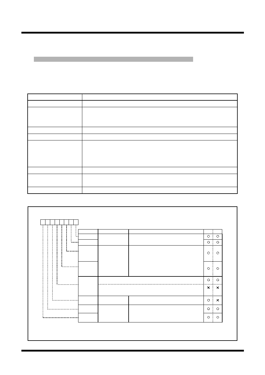
98
Tentative Specifications REV.A
Mitsubishi microcomputers
M16C / 62T Group
SINGLE-CHIP 16-BIT CMOS MICROCOMPUTER
S
pecifications in this manual are tentative and subject to change.
Under
development
Timer B
Item
Specification
Count source
f
1
, f
8
, f
32
, f
C32
Count operation
· Up count
· Counter value "0000
16
" is transferred to reload register at measurement
pulse's effective edge and the timer continues counting
Count start condition
Count start flag is set (= 1)
Count stop condition
Count start flag is reset (= 0)
Interrupt request generation timing · When measurement pulse's effective edge is input
(Note 1)
· When an overflow occurs. (Simultaneously, the timer Bi overflow flag
changes to "1". The timer Bi overflow flag changes to "0" when the count
start flag is "1" and a value is written to the timer Bi mode register.)
TBi
IN
pin function
Measurement pulse input
Read from timer
When timer Bi register is read, it indicates the reload register's content
(measurement result)
(Note 2)
Write to timer
Cannot be written to
Table 1.17.8. Timer specifications in pulse period/pulse width measurement mode
Figure 1.17.19. Timer Bi mode register in pulse period/pulse width measurement mode
Note 1: An interrupt request is not generated when the first effective edge is input after the timer has started counting.
Note 2: The value read out from the timer Bi register is indeterminate until the second effective edge is input after the timer.
Timer Bi mode register
Symbol
Address
When reset
TBiMR(i=0 to 5)
039B
16
to 039D
16
00XX0000
2
035B
16
to 035D
16
00XX0000
2
Bit name
Bit symbol
W
R
b7
b6
b5
b4
b3
b2
b1
b0
Operation mode
select bit
1 0 : Pulse period / pulse width
measurement mode
b1 b0
TMOD1
TMOD0
MR0
Measurement mode
select bit
MR2
MR1
MR3
TCK1
TCK0
0
1
0 0 : Pulse period measurement (Interval between
measurement pulse's falling edge to falling edge)
0 1 : Pulse period measurement (Interval between
measurement pulse's rising edge to rising edge)
1 0 : Pulse width measurement (Interval between
measurement pulse's falling edge to rising edge,
and between rising edge to falling edge)
1 1 : Inhibited
Function
b3 b2
Nothing is assigned (i = 1, 2, 4, 5).
In an attempt to write to this bit, write "0". The value, if read, turns out to be
indeterminate.
Count source
select bit
Timer Bi overflow
flag ( Note 1)
0 : Timer did not overflow
1 : Timer has overflowed
0 0 : f
1
0 1 : f
8
1 0 : f
32
1 1 : f
C32
b7 b6
Note 1: The timer Bi overflow flag changes to "0" when the count start flag is "1" and a value is written to the
timer Bi mode register. This flag cannot be set to "1" by software.
Note 2: Timer B0, timer B3.
Note 3: Timer B1, timer B2, timer B4, timer B5.
0 (Fixed to "0" in pulse period/pulse width measurement mode; i = 0, 3)
(Note 2)
(Note 3)
(3) Pulse period/pulse width measurement mode
In this mode, the timer measures the pulse period or pulse width of an external signal. (See Table 1.17.8.)
M30623(80-pin package), timer B1 has no input pin, so can not use this function.
Figure 1.17.19 shows the timer Bi mode register in pulse period/pulse width measurement mode. Figure
1.17.20 shows the operation timing when measuring a pulse period. Figure 1.17.21 shows the operation
timing when measuring a pulse width
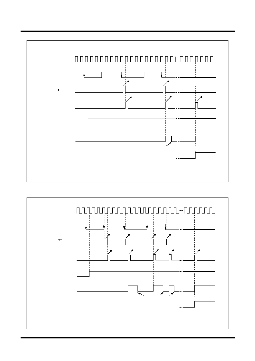
99
Tentative Specifications REV.A
Mitsubishi microcomputers
M16C / 62T Group
SINGLE-CHIP 16-BIT CMOS MICROCOMPUTER
S
pecifications in this manual are tentative and subject to change.
Under
development
Timer B
Figure 1.17.21. Operation timing when measuring a pulse width
Measurement pulse
"H"
Count source
Count start flag
Timer Bi interrupt
request bit
Timing at which counter
reaches "0000
16
"
"1"
"1"
Transfer
(measured value)
Transfer
(measured value)
"L"
"0"
"0"
Timer Bi overflow flag
"1"
"0"
Note 1: Counter is initialized at completion of measurement.
Note 2: Timer has overflowed.
(Note 1)
(Note 1)
(Note 1)
Transfer
(measured
value)
(Note 1)
Cleared to "0" when interrupt request is accepted, or cleared by software.
(Note 2)
Transfer
(indeterminate
value)
Reload register counter
transfer timing
Figure 1.17.20. Operation timing when measuring a pulse period
Count source
Measurement pulse
Count start flag
Timer Bi interrupt
request bit
Timing at which counter
reaches "0000
16
"
"H"
"1"
Transfer
(indeterminate value)
"L"
"0"
"0"
Timer Bi overflow flag
"1"
"0"
Note 1: Counter is initialized at completion of measurement.
Note 2: Timer has overflowed.
(Note 1)
(Note 1)
When measuring measurement pulse time interval from falling edge to falling edge
(Note 2)
Cleared to "0" when interrupt request is accepted, or cleared by software.
Transfer
(measured value)
"1"
Reload register counter
transfer timing
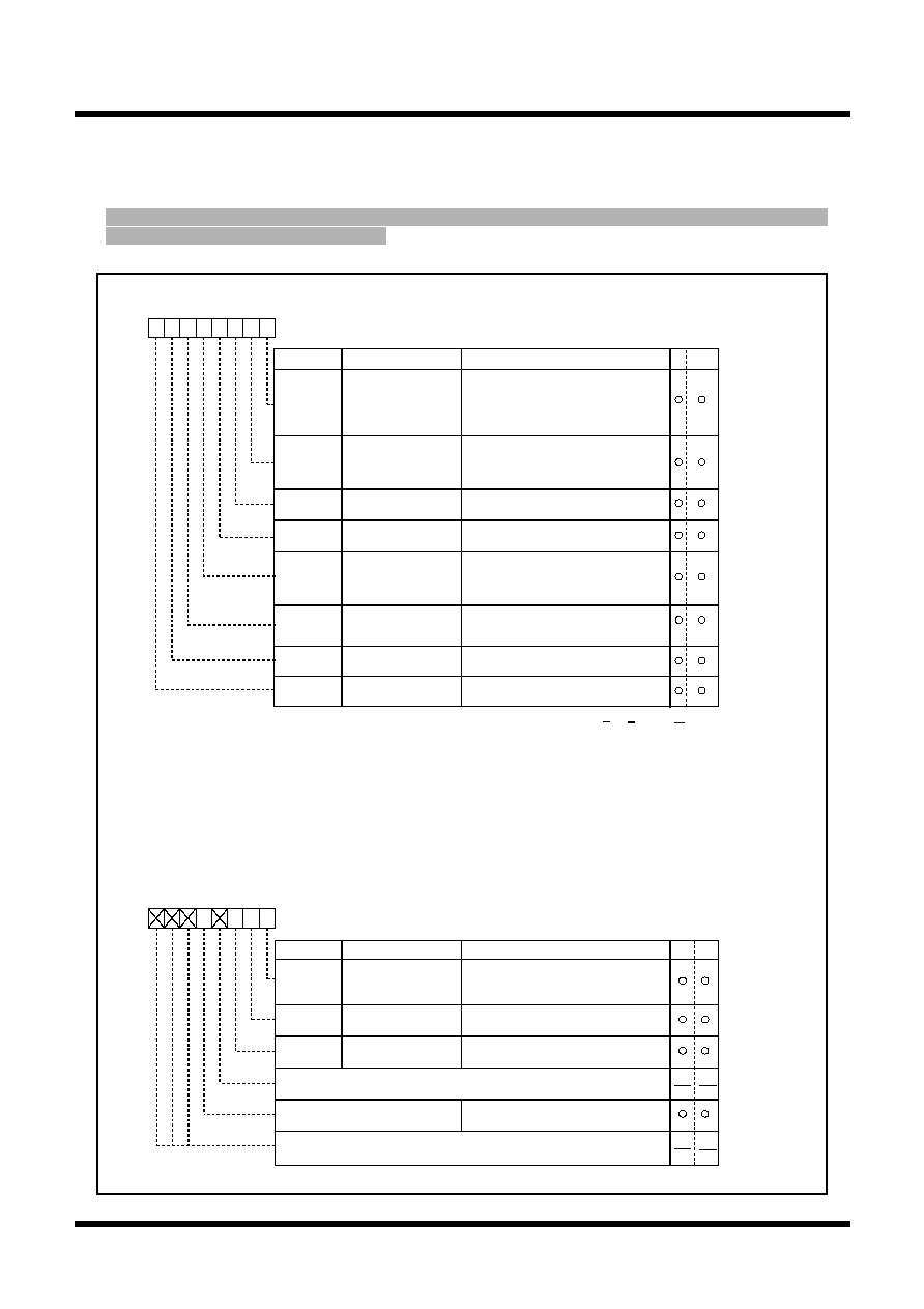
100
Tentative Specifications REV.A
Mitsubishi microcomputers
M16C / 62T Group
SINGLE-CHIP 16-BIT CMOS MICROCOMPUTER
S
pecifications in this manual are tentative and subject to change.
Under
development
Timers' functions for three-phase motor control
Three-phase PWM control register 0
Symbol
Address
When reset
INVC0
0348
16
00
16
b7
b6
b5
b4 b3
b2
b1
b0
Effective interrupt output
polarity select bit
(Note4)
INV00
Bit symbol
Bit name
Description
R
W
INV01
Effective interrupt output
specification bit
(Note4)
INV02
Mode select bit
(Note 2)
INV04
Positive and negative
phases concurrent L
output disable function
enable bit
INV07
Software trigger bit
INV06
Modulation mode select
bit (Note 3)
INV05
Positive and negative
phases concurrent L
output detect flag
INV03
Output control
bit
0: A timer B2 interrupt occurs when the timer
A1 reload control signal is "1".
1: A timer B2 interrupt occurs when the timer
A1 reload control signal is "0".
Effective only in three-phase mode 1
0: Not specified.
1: Selected by the effective interrupt output
polarity selection bit.
Effective only in three-phase mode 1
0: Normal mode
1: Three-phase PWM output mode
0: Output disabled
1: Output enabled
0: Feature disabled
1: Feature enabled
0: Not detected yet
1: Already detected
0: Triangular wave modulation mode
1: Sawtooth wave modulation mode
1: Trigger generated
The value, when read, is "0".
(Note 1)
Note 1:
Note 2:
Note 3:
Note 4:
No value other than "0" can be written.
Selecting three-phase PWM output mode causes P8
0
, P8
1
, and P7
2
through P7
5
to output U, U, V, V, W, and W, and works the
timer for setting short circuit prevention time, the U, V, W phase output control circuits, and the circuit for setting timer B2 interrupt
frequency.
In triangular wave modulation mode:
The short circuit prevention timer starts in synchronization with the falling edge of timer Ai output.
The data transfer from the three-phase buffer register to the three-phase output shift register is made only once in synchronization
with the transfer trigger signal after writing to the three-phase output buffer register.
In sawtooth wave modulation mode:
The short circuit prevention timer starts in synchronization with the falling edge of timer A output and with the transfer trigger signal.
The data transfer from the three-phase output buffer register to the three-phase output shift register is made with respect to every
transfer trigger.
To write "1" both to bit 0 (INV00) and bit 1 (INV01) of the three-phase PWM control register, set in advance the content of the timer
B2 interrupt occurrences frequency set counter.
T
hree-phase PWM control register 1
Symbol
Address When
reset
INVC1
0349
16
00
16
Bit name
Description
Bit symbol
W
R
INV10
INV11
INV12
Timer Ai start trigger
signal select bit
Timer A1-1, A2-1, A4-1
control bit
Short circuit timer count
source select bit
0: Timer B2 overflow signal
1: Timer B2 overflow signal,
signal for writing to timer B2
0: Three-phase mode 0
1: Three-phase mode 1
0 : Not to be used
1 : f
1
/2
b7 b6
b5
b4
b3
b2
b1 b0
Noting is assigned.
In an attempt to write to these bits, write "0". The value, if read, turns out to be "0".
Noting is assigned.
In an attempt to write to this bit, write "0". The value, if read, turns out to be "0".
Reserved bit
Always set to "0"
0
Note 1: To use three-phase PWM output mode, write "1" to INV12.
Figure1.18.1. Registers related to timers for three-phase motor control
Timers' functions for three-phase motor control
Use of more than one built-in timer A and timer B provides the means of outputting three-phase motor
driving waveforms.
__
___
In M30623(80-pin package), the pins V, V, W, and W for three-phase motor control have no corresponding
external pin. So, do not use this function.
Figures 1.18.1 to 1.18.3 show registers related to timers for three-phase motor control.
101
Tentative Specifications REV.A
Mitsubishi microcomputers
M16C / 62T Group
SINGLE-CHIP 16-BIT CMOS MICROCOMPUTER
S
pecifications in this manual are tentative and subject to change.
Under
development
Timers' functions for three-phase motor control
Three-phase output buffer register 0
Symbol
Address
When reset
IDB0
034A
16
00
16
Bit name
Function
Bit Symbol
W
R
b7
b6
b5
b4
b3 b2
b1
b0
Nothing is assigned.
In an attempt to write to these bits, write "0". The value, if read, turns out to be "0".
DU0
DUB0
DV0
DW0
DVB0
DWB0
U phase output buffer 0
Setting in U phase output buffer 0
V phase output buffer 0
W phase output buffer 0
U phase output buffer 0
V phase output buffer 0
W phase output buffer 0
Setting in V phase output buffer 0
Setting in W phase output buffer 0
Setting in W phase output buffer 0
Setting in V phase output buffer 0
Setting in U phase output buffer 0
Three-phase output buffer register 1
Symbol
Address
When reset
IDB1
034B
16
00
16
Bit name
Function
Bit Symbol
W
R
b7
b6 b5
b4
b3
b2
b1
b0
Nothing is assigned.
In an attempt to write to these bits, write "0". The value, if read, turns out to be "0".
DU1
DUB1
DV1
DW1
DVB1
DWB1
U phase output buffer 1
Setting in U phase output buffer 1
V phase output buffer 1
W phase output buffer 1
U phase output buffer 1
V phase output buffer 1
W phase output buffer 1
Setting in V phase output buffer 1
Setting in W phase output buffer 1
Setting in W phase output buffer 1
Setting in V phase output buffer 1
Setting in U phase output buffer 1
Dead time timer
Symbol
Address
When reset
DOT
034C
16
Indeterminate
Function
Values that can be set
W
R
b7
b0
Set dead time timer
1 to 255
Timer B2 interrupt occurrences frequency set counter
Symbol
Address
When reset
ICTB2
034D
16
Indeterminate
Function
Values that can be set
W
R
b3
b0
Set occurrence frequency of timer B2
interrupt request
1 to 15
Note: When executing read instruction of this register, the contents of three-phase shift
register is read out.
Note: When executing read instruction of this register, the contents of three-phase shift
register is read out.
Note1: In setting 1 to bit 1 (INV01) - the effective interrupt output specification bit - of three-
phase PWM control register 0, do not change the B2 interrupt occurrences frequency
set counter to deal with the timer function for three-phase motor control.
Note2: Do not write at the timing of an overflow occurrence in timer B2.
Figure 1.18.2. Registers related to timers for three-phase motor control
102
Tentative Specifications REV.A
Mitsubishi microcomputers
M16C / 62T Group
SINGLE-CHIP 16-BIT CMOS MICROCOMPUTER
S
pecifications in this manual are tentative and subject to change.
Under
development
Timers' functions for three-phase motor control
Figure 1.18.3. Registers related to timers for three-phase motor control
Symbol
Address
When reset
TA11
0343
16
,0342
16
Indeterminate
TA21
0345
16
,0344
16
Indeterminate
TA41
0347
16
,0346
16
Indeterminate
b7
b0 b7
b0
(b15)
(b8)
W
R
Counts an internal count source
0000
16
to FFFF
16
Function
Values that can be set
Timer Ai-1 register (Note)
Note: Read and write data in 16-bit units.
Symbol
Address
When reset
TA1
0389
16
,0388
16
Indeterminate
TA2
038B
16
,038A
16
Indeterminate
TA4
038F
16
,038E
16
Indeterminate
TB2
0395
16
,0394
16
Indeterminate
b7
b0
b7
b0
(b15)
(b8)
W
R
· Timer mode
0000
16
to FFFF
16
Counts an internal count source
Function
Values that can be set
· One-shot timer mode
0000
16
to FFFF
16
Counts a one shot width
Note: Read and write data in 16-bit units.
Timer Ai register (Note)
TA1TGL
Symbol
Address
When reset
TRGSR
0383
16
00
16
Timer A1 event/trigger
select bit
0 0 :
Input on TA1
IN
is selected (Note)
0 1 : TB2 overflow is selected
1 0 : TA0 overflow is selected
1 1 : TA2 overflow is selected
Trigger select register
Bit name
Function
Bit symbol
b0
0 0 :
Input on TA2
IN
is selected (Note)
0 1 : TB2 overflow is selected
1 0 : TA1 overflow is selected
1 1 : TA3 overflow is selected
0 0 :
Input on TA3
IN
is selected (Note)
0 1 : TB2 overflow is selected
1 0 : TA2 overflow is selected
1 1 : TA4 overflow is selected
0 0 :
Input on TA4
IN
is selected (Note)
0 1 : TB2 overflow is selected
1 0 : TA3 overflow is selected
1 1 : TA0 overflow is selected
Timer A2 event/trigger
select bit
Timer A3 event/trigger
select bit
Timer A4 event/trigger
select bit
W
R
TA1TGH
TA2TGL
TA2TGH
TA3TGL
TA3TGH
TA4TGL
TA4TGH
b1 b0
b3 b2
b5 b4
b7 b6
Note: Set the corresponding port direction register to "0".
b7
b6
b5
b4 b3
b2
b1
Symbol
Address
When reset
TABSR
0380
16
00
16
Count start flag
Bit name
Function
Bit symbol
W
R
b7 b6
b5
b4
b3
b2
b1 b0
Timer B2 count start flag
Timer B1 count start flag
Timer B0 count start flag
Timer A4 count start flag
Timer A3 count start flag
Timer A2 count start flag
Timer A1 count start flag
Timer A0 count start flag
0 : Stops counting
1 : Starts counting
TB2S
TB1S
TB0S
TA4S
TA3S
TA2S
TA1S
TA0S
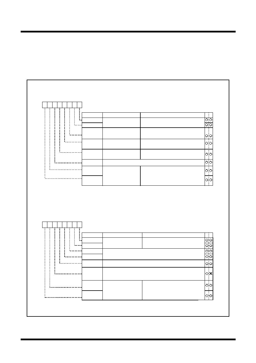
103
Tentative Specifications REV.A
Mitsubishi microcomputers
M16C / 62T Group
SINGLE-CHIP 16-BIT CMOS MICROCOMPUTER
S
pecifications in this manual are tentative and subject to change.
Under
development
Timers' functions for three-phase motor control
Bit name
Timer Ai mode register
Symbol
Address
When reset
TA1MR
0397
16
00
16
TA2MR
0398
16
00
16
TA3MR
039A
16
00
16
Function
Bit symbol
b7
b6
b5
b4
b3
b2 b1
b0
Operation mode
select bit
1 0 : One-shot timer mode
b1 b0
TMOD1
TMOD0
MR0
Pulse output function
select bit
0 (Must always be "0" in three-phase PWM
output mode)
MR2
MR1
MR3
0 (Must always be "0" in one-shot timer mode)
0 0 : f
1
0 1 : f
8
1 0 : f
32
1 1 : f
C32
b7 b6
TCK1
TCK0
Count source select bit
1 0
0
1 : Selected by event/trigger select
register
Trigger select bit
External trigger select
bit
W
R
Timer B2 mode register
Symbol
Address
When reset
TB2MR
039D
16
00XX0000
2
Bit name
Function
Bit symbol
W
R
b7
b6
b5 b4
b3
b2
b1
b0
Operation mode select bit
0 0 : Timer mode
b1 b0
TMOD1
TMOD0
MR0
Invalid in timer mode
Can be "0" or "1"
MR2
MR1
MR3
0 0 : f
1
0 1 : f
8
1 0 : f
32
1 1 : f
C32
TCK1
TCK0
Count source select bit
0
Invalid in timer mode.
This bit can neither be set nor reset. When read in timer mode,
its content is indeterminate.
0
0 (Fixed to "0" in timer mode ; i = 0)
b7 b6
1
0
Invalid in three-phase PWM output mode
Can be "0" or "1"
Figure 1.18.4. Timer mode registers in three-phase waveform mode
Three-phase motor driving waveform output mode (three-phase waveform mode)
Setting "1" in the mode select bit (bit 2 at 0348
16
) shown in Figure 1.18.1 - causes three-phase waveform
mode that uses four timers A1, A2, A4, and B2 to be selected. As shown in Figure 1.18.4, set timers A1,
A2, and A4 in one-shot timer mode, set the trigger in timer B2, and set timer B2 in timer mode using the
respective timer mode registers.

104
Tentative Specifications REV.A
Mitsubishi microcomputers
M16C / 62T Group
SINGLE-CHIP 16-BIT CMOS MICROCOMPUTER
S
pecifications in this manual are tentative and subject to change.
Under
development
Timers' functions for three-phase motor control
Figure 1.18.5 shows the block diagram for three-phase waveform mode. In three-phase waveform mode,
___
___
the positive-phase waveforms (U phase, V phase, and W phase) and negative waveforms (U phase, V
___
phase, and W phase), six waveforms in total, are output from P8
0
,P8
1
, P7
2
, P7
3
, P7
4
, and P7
5
as active
___
on the "L" level. Of the timers used in this mode, timer A4 controls the U phase and U phase, timer A1
___
___
controls the V phase and V phase, and timer A2 controls the W phase and W phase respectively; timer B2
controls the periods of one-shot pulse output from timers A4, A1, and A2.
In outputting a waveform, dead time can be set so as to cause the "L" level of the positive waveform
___
output (U phase, V phase, and W phase) not to lap over the "L" level of the negative waveform output (U
___
___
phase, V phase, and W phase).
To set short circuit time, use three 8-bit timers sharing the reload register for setting dead time. A value
from 1 through 255 can be set as the count of the timer for setting dead time. The timer for setting dead
time works as a one-shot timer. If a value is written to the dead timer (034C
16
), the value is written to the
reload register shared by the three timers for setting dead time.
Any of the timers for setting dead time takes the value of the reload register into its counter, if a start
trigger comes from its corresponding timer, and performs a down count in line with the clock source
selected by the dead time timer count source select bit (bit 2 at 0349
16
). The timer can receive another
trigger again before the workings due to the previous trigger are completed. In this instance, the timer
performs a down count from the reload register's content after its transfer, provoked by the trigger, to the
timer for setting dead time.
Since the timer for setting dead time works as a one-shot timer, it starts outputting pulses if a trigger
comes; it stops outputting pulses as soon as its content becomes 00
16
, and waits for the next trigger to
come.
___
___
The positive waveforms (U phase, V phase, and W phase) and the negative waveforms (U phase, V
___
phase, and W phase) in three-phase waveform mode are output from respective ports by means of
setting "1" in the output control bit (bit 3 at 0348
16
). Setting "0" in this bit causes the ports to be the state
of set by port direction register. This bit can be set to "0" not only by use of the applicable instruction, but
_______
by entering a falling edge in the NMI terminal or by resetting. Also, if "1" is set in the positive and negative
phases concurrent L output disable function enable bit (bit 4 at 0348
16
) causes one of the pairs of U
___
___
___
phase and U phase, V phase and V phase, and W phase and W phase concurrently go to "L", as a result,
the port become the state of set by port direction register.
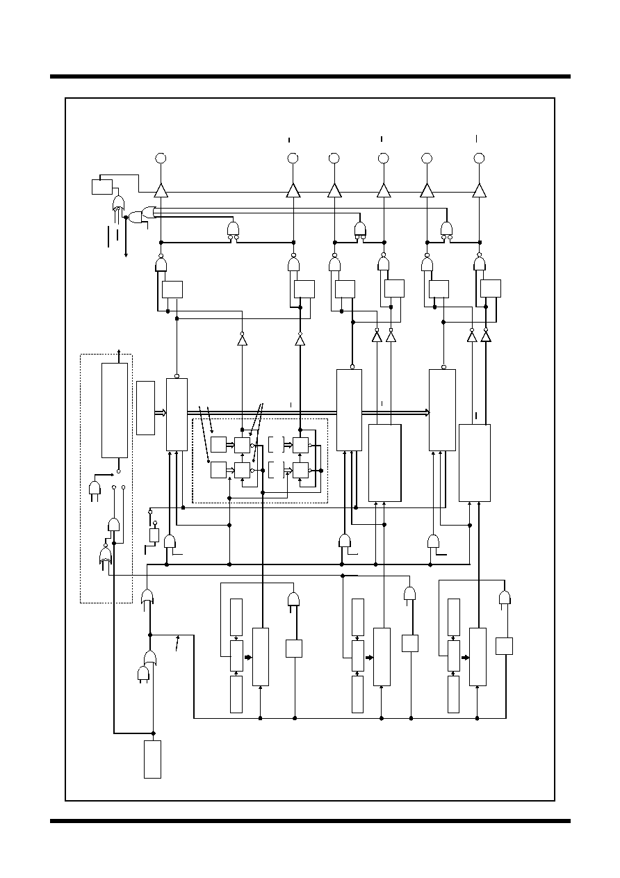
105
Tentative Specifications REV.A
Mitsubishi microcomputers
M16C / 62T Group
SINGLE-CHIP 16-BIT CMOS MICROCOMPUTER
S
pecifications in this manual are tentative and subject to change.
Under
development
Timers' functions for three-phase motor control
Timer B2
(Timer mode)
Overflow
Interrupt occurrence
frequency set counter
Interrupt request bit
U(P8
0
)
U(P8
1
)
V(P7
2
)
V(P7
3
)
W(P7
4
)
W(P7
5
)
NMI
RESET
R
D
D
T
Q
D
T
Q
D
T
Q
D
T
Q
For short circuit
prevention
D
T
Q
D
T
Q
Q
INV03
INV05
Diagram for switching to P8
0
, P8
1
, and to P7
2
- P7
5
is not shown.
INV04
Timer A4 counter
(One-shot timer mode)
(One-shot timer mode)
(One-shot timer mode)
Trigger
Timer A4
Reload
Timer A4-1
Timer A1 counter
Trigger
Timer A1
Reload
Timer A1-1
Timer A2 counter
Trigger
Timer A2
Reload
Timer A2-1
INV0
7
T
Q
INV11
Dead time timer setting (8)
INV00
1
0
INV01
INV11
DU0
DU1
T
DQ
T
DQ
DUB0
DUB1
T
DQ
T
DQ
U phase output control circuit
U phase output signal
U phase output signal
V phase output
control circuit
To be set to "0" when timer A4 stops
T
Q
INV11
To be set to "0" when timer A1 stops
T
Q
INV11
To be set to "0" when timer A2 stops
U phase output
control circuit
V phase output signal
W phase output signal
V phase output signal
W phase output signal
Signal to be
written to B2
Trigger signal for
timer Ai start
Trigger signal for
transfer
INV10
Circuit foriInterrupt occurrence
frequency set counter
Bit 0 at 034B
16
Bit 0 at 034A
16
Three-phase output
shift register
(U phase)
Control signal for timer A4 reload
f
1
INV12
1
1/2
n = 1 to 15
Reload register
n = 1 to 255
Dead time timer setting
n = 1 to 255
Dead time timer setting (8)
n = 1 to 255
n = 1 to 255
Trigger
INV06
Trigger
Trigger
Trigger
Trigger
Trigger
INV06
INV06
(Note)
Note: To use three-phase output mode, write "1" to INV
12
.
Figure 1.18.5. Block diagram for three-phase waveform mode

106
Tentative Specifications REV.A
Mitsubishi microcomputers
M16C / 62T Group
SINGLE-CHIP 16-BIT CMOS MICROCOMPUTER
S
pecifications in this manual are tentative and subject to change.
Under
development
Timers' functions for three-phase motor control
Triangular wave modulation
To generate a PWM waveform of triangular wave modulation, set "0" in the modulation mode select bit
(bit 6 at 0348
16
). Also, set "1" in the timers A4-1, A1-1, A2-1 control bit (bit 1 at 0349
16
). In this mode, each
of timers A4, A1, and A2 has two timer registers, and alternately reloads the timer register's content to the
counter every time timer B2 counter's content becomes 0000
16
. If "1" is set to the effective interrupt
output specification bit (bit 1 at 0348
16
), the frequency of interrupt requests that occur every time the timer
B2 counter's value becomes 0000
16
can be set by use of the timer B2 counter (034D
16
) for setting the
frequency of interrupt occurrences. The frequency of occurrences is given by (setting; setting
0).
Setting "1" in the effective interrupt output specification bit (bit 1 at 0348
16
) provides the means to choose
which value of the timer A1 reload control signal to use, "0" or "1", to cause timer B2's interrupt request to
occur. To make this selection, use the effective interrupt output polarity selection bit (bit 0 at 0348
16
).
An example of U phase waveform is shown in Figure 1.18.6, and the description of waveform output
workings is given below. Set "1" in DU0 (bit 0 at 034A
16
). And set "0" in DUB0 (bit 1 at 034A
16
). In
addition, set "0" in DU1 (bit 0 at 034B
16
) and set "1" in DUB1 (bit 1 at 034B
16
). Also, set "0" in the effective
interrupt output specification bit (bit 1 at 0348
16
) to set a value in the timer B2 interrupt occurrence
frequency set counter. By this setting, a timer B2 interrupt occurs when the timer B2 counter's content
becomes 0000
16
as many as (setting) times. Furthermore, set "1" in the effective interrupt output specifi-
cation bit (bit 1 at 0348
16
), set in the effective interrupt polarity select bit (bit 0 at 0348
16
) and set "1" in the
interrupt occurrence frequency set counter(034D
16
). These settings cause a timer B2 interrupt to occur
every other interval when the U phase output goes to "H".
When the timer B2 counter's content becomes 0000
16
, timer A4 starts outputting one-shot pulses. In this
instance, the content of DU1 (bit 0 at 034B
16
) and that of DU0 (bit 0 at 034A
16
) are set in the three-phase
output shift register (U phase), the content of DUB1 (bit 1 at 034B
16
) and that of DUB0 (bit 1 at 034A
16
)
___
are set in the three-phase shift register (U phase). After triangular wave modulation mode is selected,
however, no setting is made in the shift register even though the timer B2 counter's content becomes
0000
16
.
___
The value of DU0 and that of DUB0 are output to the U terminal (P8
0
) and to the U terminal (P8
1
)
respectively. When the timer A4 counter counts the value written to timer A4 (038F
16
, 038E
16
) and when
timer A4 finishes outputting one-shot pulses, the three-phase shift register's content is shifted one posi-
___
tion, and the value of DU1 and that of DUB1 are output to the U phase output signal and to U phase output
signal respectively. At this time, one-shot pulses are output from the timer for setting dead time used for
___
setting the time over which the "L" level of the U phase waveform does not lap over the "L" level of the U
phase waveform, which has the opposite phase of the former. The U phase waveform output that started
from the "H" level keeps its level until the timer for setting dead time finishes outputting one-shot pulses
even though the three-phase output shift register's content changes from "1" to "0" by the effect of the
one-shot pulses. When the timer for setting dead time finishes outputting one-shot pulses, "0" already
shifted in the three-phase shift register goes effective, and the U phase waveform changes to the "L"
level. When the timer B2 counter's content becomes 0000
16
, the timer A4 counter starts counting the
value written to timer A4-1 (0347
16
, 0346
16
), and starts outputting one-shot pulses. When timer A4 fin-
ishes outputting one-shot pulses, the three-phase shift register's content is shifted one position, but if the
three-phase output shift register's content changes from "0" to "1" as a result of the shift, the output level
changes from "L" to "H" without waiting for the timer for setting dead time to finish outputting one-shot
pulses. A U phase waveform is generated by these workings repeatedly. With the exception that the
three-phase output shift register on the U phase side is used, the workings in generating a U phase
waveform, which has the opposite phase of the U phase waveform, are the same as in generating a U
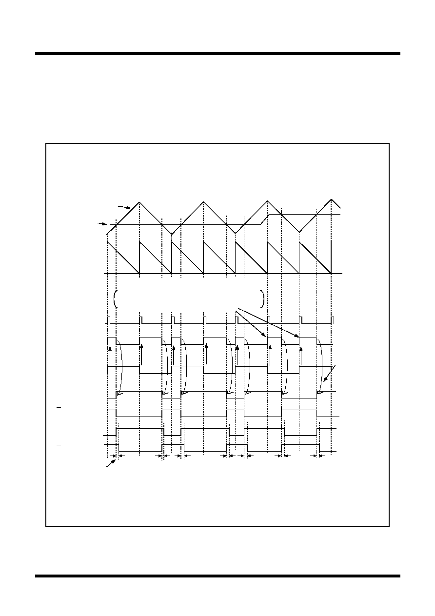
107
Tentative Specifications REV.A
Mitsubishi microcomputers
M16C / 62T Group
SINGLE-CHIP 16-BIT CMOS MICROCOMPUTER
S
pecifications in this manual are tentative and subject to change.
Under
development
Timers' functions for three-phase motor control
Timer A4 output
Trigger signal for
timer Ai start
(timer B2 overflow
signal)
B2
U phase
Dead time
A carrier wave of triangular waveform
Carrier wave
Signal wave
Timber B2 interrupt occurres
Rewriting timer A4 and timer A4-1.
Possible to set the number of overflows to generate an
interrupt by use of the interrupt occurrences frequency
set circuit
U phase
output signal
m
n
n
m
p
o
Note: Set to triangular wave modulation mode and to three-phase mode 1.
Control signal for
timer A4 reload
m
The three-phase
shift register
shifts in
synchronization
with the falling
edge of the A4
output.
U phase
U phase
output signal
Figure 1.18.6. Timing chart of operation (1)
phase waveform. In this way, a waveform can be picked up from the applicable terminal in a manner in
which the "L" level of the U phase waveform doesn't lap over that of the U phase waveform, which has the
opposite phase of the U phase waveform. The width of the "L" level too can be adjusted by varying the
___
___
values of timer B2, timer A4, and timer A4-1. In dealing with the V and W phases, and V and W phases,
the latter are of opposite phase of the former, have the corresponding timers work similarly to dealing with
___
the U and U phases to generate an intended waveform.
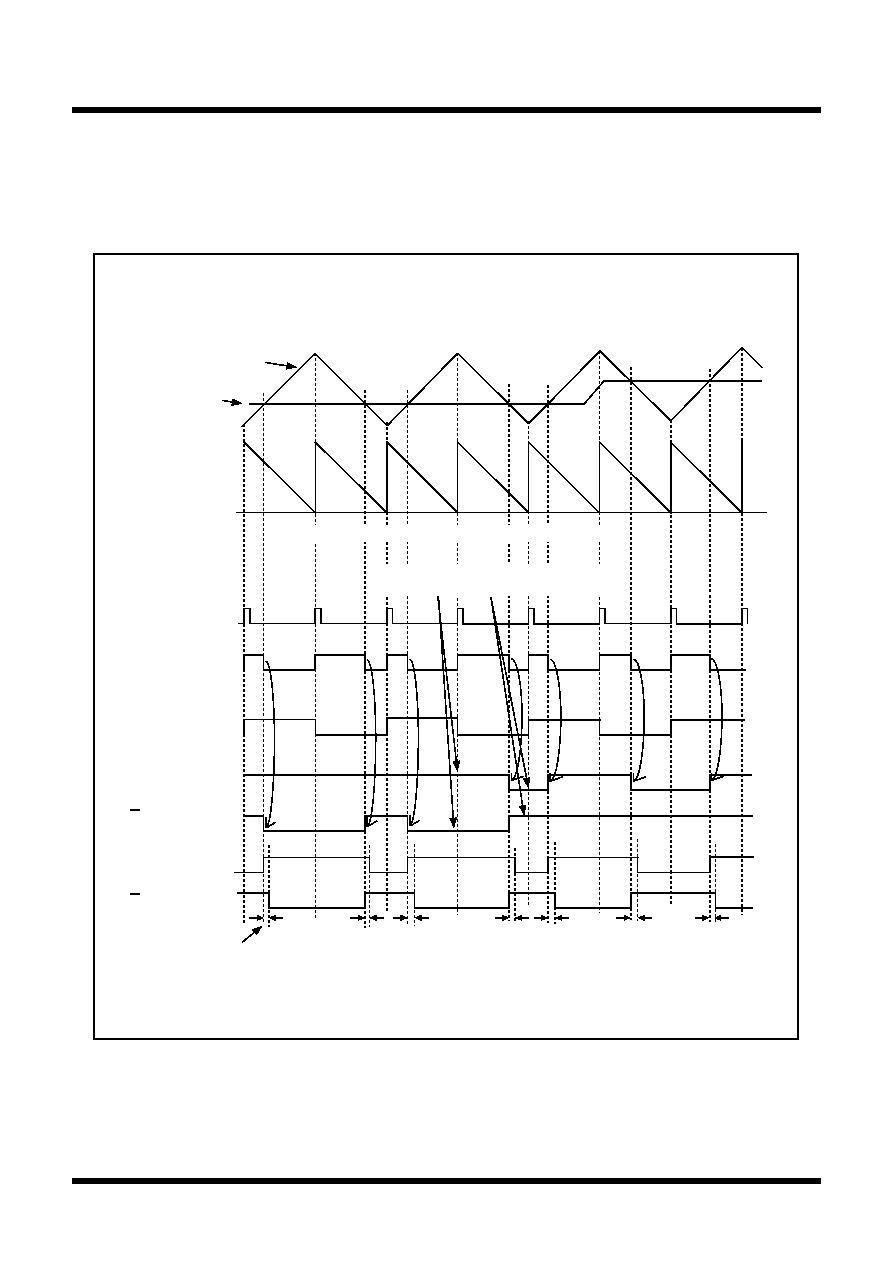
108
Tentative Specifications REV.A
Mitsubishi microcomputers
M16C / 62T Group
SINGLE-CHIP 16-BIT CMOS MICROCOMPUTER
S
pecifications in this manual are tentative and subject to change.
Under
development
Timers' functions for three-phase motor control
Figure 1.18.7. Timing chart of operation (2)
Timer A4 output
Trigger signal for
timer Ai start
(timer B2 overflow
signal)
Timer B2
U phase
Dead time
A carrier wave of triangular waveform
Carrier wave
Signal wave
Rewriting timer A4 every timer B2 interrupt occurres.
U phase
output signal
m
n
n
m
p
o
Note: Set to triangular wave modulation mode and to three-phase mode 0.
Control signal for
timer A4 reload
m
U phase
U phase
output signal
Timer B2 interrupt occurres.
Rewriting three-phase buffer register.
Assigning certain values to DU0 (bit 0 at 034A
16
) and DUB0 (bit 1 at 034A
16
), and to DU1 (bit 0 at 034B
16
)
and DUB1 (bit 1 at 034B
16
) allows the user to output the waveforms as shown in Figure 1.18.7, that is, to
___
___
output the U phase alone, to fix U phase to "H", to fix the U phase to "H," or to output the U phase alone.

109
Tentative Specifications REV.A
Mitsubishi microcomputers
M16C / 62T Group
SINGLE-CHIP 16-BIT CMOS MICROCOMPUTER
S
pecifications in this manual are tentative and subject to change.
Under
development
Timers' functions for three-phase motor control
Sawtooth modulation
To generate a PWM waveform of sawtooth wave modulation, set "1" in the modulation mode select bit (bit
6 at 0348
16
). Also, set "0" in the timers A4-1, A1-1, and A2-1 control bit (bit 1 at 0349
16
). In this mode, the
timer registers of timers A4, A1, and A2 comprise conventional timers A4, A1, and A2 alone, and reload
the corresponding timer register's content to the counter every time the timer B2 counter's content be-
comes 0000
16
. The effective interrupt output specification bit (bit 1 at 0348
16
) and the effective interrupt
output polarity select bit (bit 0 at 0348
16
) go nullified.
An example of U phase waveform is shown in Figure 75, and the description of waveform output workings
is given below. Set "1" in DU0 (bit 0 at 034A
16
), and set "0" in DUB0 (bit 1 at 034A
16
). In addition, set "0"
in DU1 (bit 0 at 034A
16
) and set "1" in DUB1 (bit 1 at 034A
16
).
When the timber B2 counter's content becomes 0000
16
, timer B2 generates an interrupt, and timer A4
starts outputting one-shot pulses at the same time. In this instance, the contents of the three-phase buffer
registers DU1 and DU0 are set in the three-phase output shift register (U phase), and the contents of
DUB1 and DUB0 are set in the three-phase output register (U phase). After this, the three-phase buffer
register's content is set in the three-phase shift register every time the timer B2 counter's content be-
comes 0000
16
.
___
The value of DU0 and that of DUB0 are output to the U terminal (P8
0
) and to the U terminal (P8
1
)
respectively. When the timer A4 counter counts the value written to timer A4 (038F
16
, 038E
16
) and when
timer A4 finishes outputting one-shot pulses, the three-phase output shift register's content is shifted one
___
position, and the value of DU1 and that of DUB1 are output to the U phase output signal and to the U
output signal respectively. At this time, one-shot pulses are output from the timer for setting dead time
used for setting the time over which the "L" level of the U phase waveform doesn't lap over the "L" level of
___
the U phase waveform, which has the opposite phase of the former. The U phase waveform output that
started from the "H" level keeps its level until the timer for setting dead time finishes outputting one-shot
pulses even though the three-phase output shift register's content changes from "1" to "0 "by the effect of
the one-shot pulses. When the timer for setting dead time finishes outputting one-shot pulses, 0 already
shifted in the three-phase shift register goes effective, and the U phase waveform changes to the "L"
level. When the timer B2 counter's content becomes 0000
16
, the contents of the three-phase buffer
registers DU1 and DU0 are set in the three-phase shift register (U phase), and the contents of DUB1 and
___
DUB0 are set in the three-phase shift register (U phase) again.
A U phase waveform is generated by these workings repeatedly. With the exception that the three-phase
___
___
output shift register on the U phase side is used, the workings in generating a U phase waveform, which
has the opposite phase of the U phase waveform, are the same as in generating a U phase waveform. In
this way, a waveform can be picked up from the applicable terminal in a manner in which the "L" level of
the U phase waveform doesn't lap over that of the U phase waveform, which has the opposite phase of
the U phase waveform. The width of the "L" level too can be adjusted by varying the values of timer B2
___
___
and timer A4. In dealing with the V and W phases, and V and W phases, the latter are of opposite phase
___
of the former, have the corresponding timers work similarly to dealing with the U and U phases to gener-
ate an intended waveform.
___
Setting "1" both in DUB0 and in DUB1 provides a means to output the U phase alone and to fix the U
phase output to "H" as shown in Figure 1.18.8.
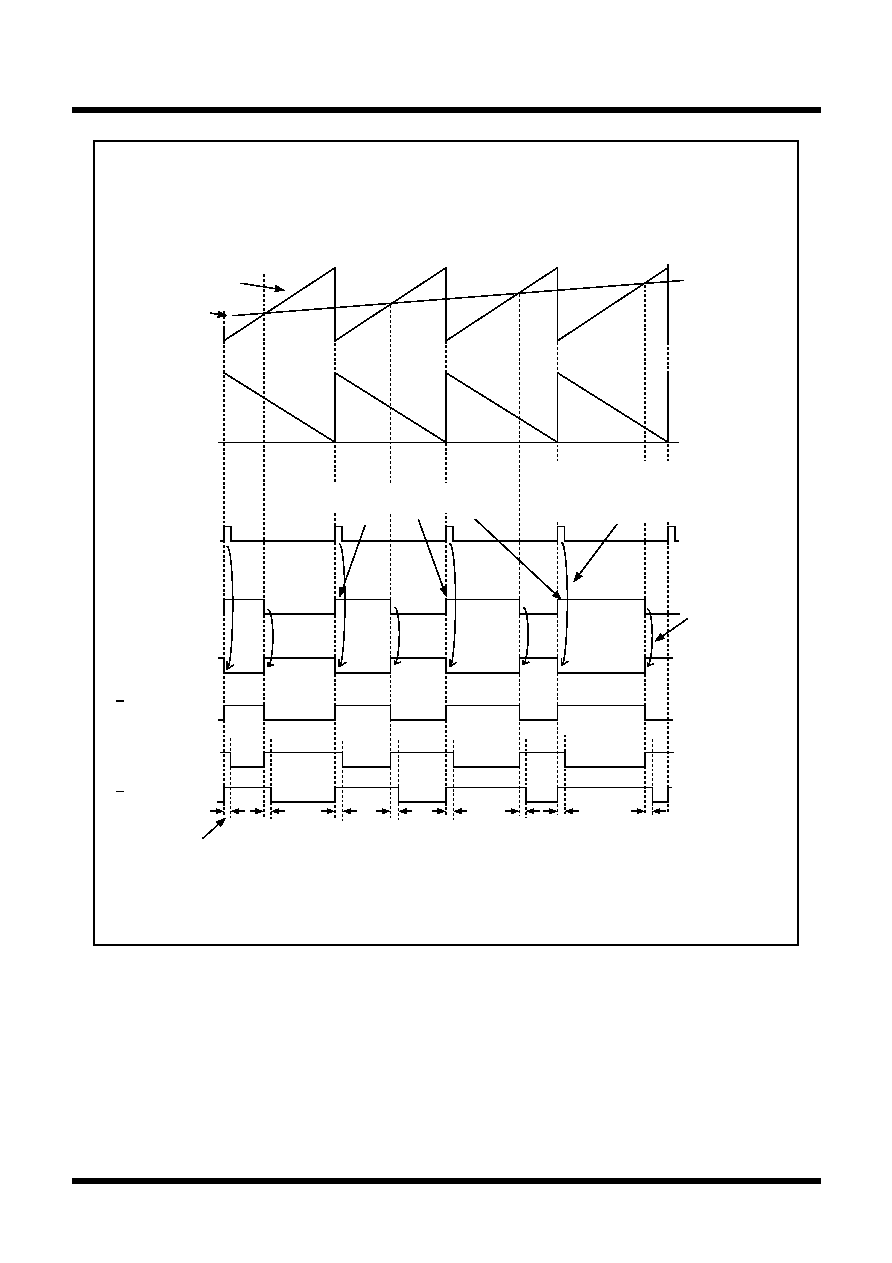
110
Tentative Specifications REV.A
Mitsubishi microcomputers
M16C / 62T Group
SINGLE-CHIP 16-BIT CMOS MICROCOMPUTER
S
pecifications in this manual are tentative and subject to change.
Under
development
Timers' functions for three-phase motor control
Timer B2
Timer A4 output
U phase
U phase
Dead time
Carrier wave
Signal wave
A carrier wave of sawtooth waveform
m
n
o
p
Note: Set to sawtooth modulation mode and to three-phase mode 0.
Interrupt occurres.
Rewriting the value of timer A4.
U phase output
signal
U phase
output signal
The three-phase
shift register
shifts in
synchronization
with the falling
edge of timer A4.
Data transfer is made from the three-
phase buffer register to the three-
phase shift register in step with the
timing of the timer B overflow.
Trigger signal for
timer Ai start
(timer B2 overflow
signal)
Figure 1.18.8. Timing chart of operation (3)
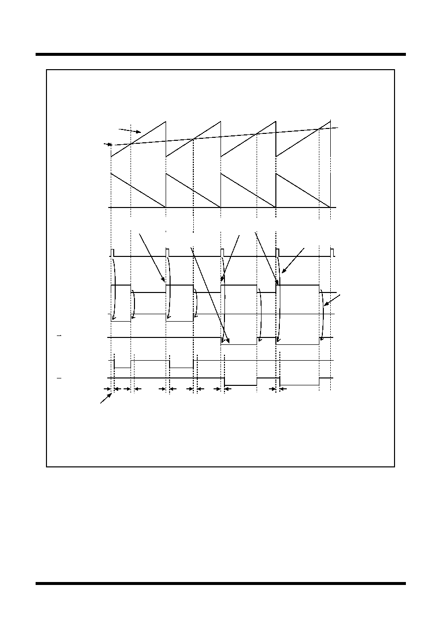
111
Tentative Specifications REV.A
Mitsubishi microcomputers
M16C / 62T Group
SINGLE-CHIP 16-BIT CMOS MICROCOMPUTER
S
pecifications in this manual are tentative and subject to change.
Under
development
Timers' functions for three-phase motor control
Timer B2
Timer A4 output
U phase
U phase
Dead time
Carrier wave
Signal wave
A carrier wave of sawtooth waveform
m
n
p
Note: Set to sawtooth modulation mode and to three-phase mode 0.
U phase
output signal
U phase
output signal
The three-phase
shift register shifts
in synchronization
with the falling
edge of timer A4.
Trigger signal for
timer Ai start
(timer B2 overflow
signal)
Interrupt occurres.
Rewriting the value of timer A4.
Rewriting three-phase
output buffer register
Data transfer is made from the three-
phase buffer register to the three-
phase shift register in step with the
timing of the timer B overflow.
Interrupt occurres.
Rewriting the value of timer A4.
Figure 1.18.9. Timing chart of operation (4)
112
Tentative Specifications REV.A
Mitsubishi microcomputers
M16C / 62T Group
SINGLE-CHIP 16-BIT CMOS MICROCOMPUTER
S
pecifications in this manual are tentative and subject to change.
Under
development
Serial I/O
Serial I/O
Serial I/O is configured as five channels: UART0, UART1, UART2, S I/O3 and S I/O4.
UART0 to 2
UART0, UART1 and UART2 each have an exclusive timer to generate a transfer clock, so they operate
independently of each other.
Figure 1.19.1 shows the block diagram of UART0, UART1 and UART2. Figures 1.19.2 and 1.19.3 show
the block diagram of the transmit/receive unit.
UARTi (i = 0 to 2) has two operation modes: a clock synchronous serial I/O mode and a clock asynchronous
serial I/O mode (UART mode). The contents of the serial I/O mode select bits (bits 0 to 2 at addresses
03A0
16
, 03A8
16
and 0378
16
) determine whether UARTi is used as a clock synchronous serial I/O or as a
UART. Although a few functions are different, UART0, UART1 and UART2 have almost the same functions.
UART0 through UART2 are almost equal in their functions with minor exceptions. UART2, in particular, is
compliant with the SIM interface with some extra settings added in clock-asynchronous serial I/O mode
(Note). It also has the bus collision detection function that generates an interrupt request if the TxD pin and
the RxD pin are different in level.
In M30623(80-pin package), UART2 has the clock-asynchronous serial I/O mode and IIC mode.
Table 1.19.1 shows the comparison of functions of UART0 through UART2, and Figures 1.19.4 to 1.19.8
show the registers related to UARTi.
Note: SIM : Subscriber Identity Module
Table 1.19.1. Comparison of functions of UART0 through UART2
Note 1: Only when clock synchronous serial I/O mode.
Note 2: Only when clock synchronous serial I/O mode and 8-bit UART mode.
Note 3: Only when UART mode.
Note 4: Using for SIM interface.
Note 5: In M30623(80-pin package), do not use this function, because CLK
2
and CTS
2
/RTS
2
have no external pin.
Note 6: Connect via pull-up resistor to V
CC
outside.
Note 7: Generally, it use in case of IE bus-emulation.
UART0
UART1
UART2
Function
CLK polarity selection
Continuous receive mode selection
LSB first / MSB first selection
Impossible
Transfer clock output from multiple
pins selection
Impossible
Impossible
Impossible
Impossible
Serial data logic switch
Impossible
Sleep mode selection
Impossible
Impossible
TxD, RxD I/O polarity switch
Impossible
Possible
CMOS output
TxD, RxD port output format
CMOS output
N-channel open-drain
output (Note 6)
Impossible
Parity error signal output
Impossible
Impossible
Bus collision detection
Impossible
Possible (Note 7)
Possible (Note 1)
Separate CTS/RTS pins
Possible (Note 1)
Possible (Note 1)
Possible (Note 3)
Possible (Note 1)
Possible (Note 1)
Possible
(Note 1)
Possible
(Note 1)
Possible
(Note 3)
Possible
Possible (Note 1)
Possible
(Note 2)
Possible
(Note 1)
Possible
(Note 4)
Possible
(Note 4)
Impossible (Note 5)
M30623
(80pin-package)
M30622
(100pin-package)
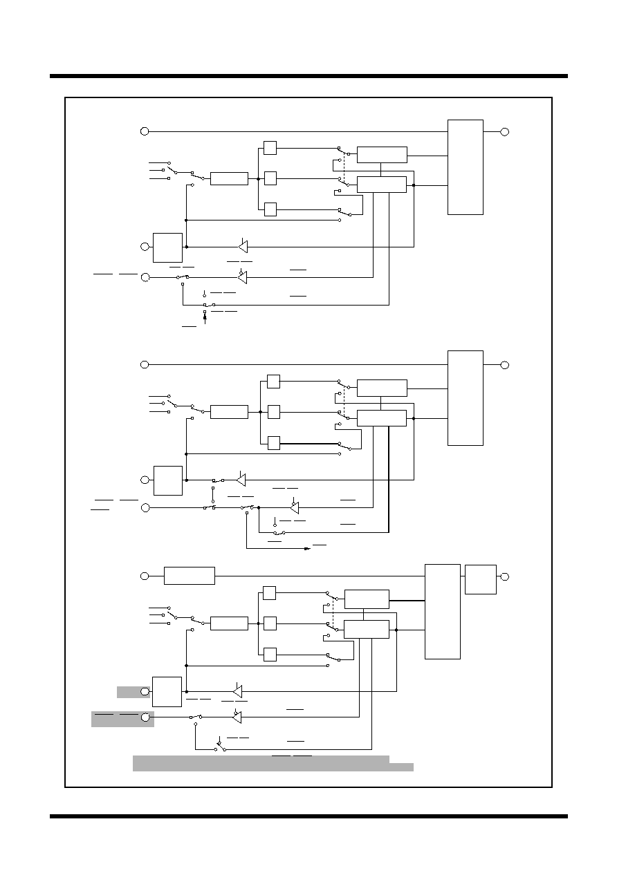
113
Tentative Specifications REV.A
Mitsubishi microcomputers
M16C / 62T Group
SINGLE-CHIP 16-BIT CMOS MICROCOMPUTER
S
pecifications in this manual are tentative and subject to change.
Under
development
Serial I/O
Figure 1.19.1. Block diagram of UARTi (i = 0 to 2)
n0 : Values set to UART0 bit rate generator (BRG0)
n1 : Values set to UART1 bit rate generator (BRG1)
n2 : Values set to UART2 bit rate generator (BRG2)
RxD
2
Reception
control circuit
Transmission
control circuit
1 / (n
2
+1)
1/16
1/16
1/2
Bit rate generator
(address 0379
16
)
Clock synchronous type
(when internal clock is selected)
UART reception
Clock synchronous type
UART transmission
Clock synchronous type
Clock synchronous type
(when internal clock is selected)
Clock synchronous type
(when external clock is
selected)
Receive
clock
Transmit
clock
CLK
2
CTS
2
/ RTS
2
f
1
f
8
f
32
Vcc
RTS
2
CTS
2
TxD
2
(UART2)
RxD polarity
reversing circuit
TxD
polarity
reversing
circuit
RxD
0
1 / (n
0
+1)
1/2
Bit rate generator
(address 03A1
16
)
Clock synchronous type
(when internal clock is selected)
UART reception
Clock synchronous type
UART transmission
Clock synchronous type
Clock synchronous type
(when internal clock is selected)
Clock synchronous type
(when external clock is
selected)
Receive
clock
Transmit
clock
CLK
0
Clock source selection
CTS
0
/ RTS
0
f
1
f
8
f
32
Reception
control circuit
Transmission
control circuit
Internal
External
Vcc
RTS
0
CTS
0
TxD
0
Transmit/
receive
unit
RxD
1
1 / (n
1
+1)
1/16
1/16
1/2
Bit rate generator
(address 03A9
16
)
Clock synchronous type
(when internal clock is selected)
UART reception
Clock synchronous type
UART transmission
Clock synchronous type
Clock synchronous type
(when internal clock is selected)
Clock synchronous type
(when external clock is
selected)
Receive
clock
Transmit
clock
CLK
1
Clock source selection
f
1
f
8
f
32
Reception
control circuit
Transmission
control circuit
Internal
External
RTS
1
CTS
1
TxD
1
(UART1)
(UART0)
CLK
polarity
reversing
circuit
CLK
polarity
reversing
circuit
CTS/RTS disabled
CTS/RTS separated
Clock output pin
select switch
CTS
1
/ RTS
1
/ CTS
0
/ CLKS
1
CTS/RTS disabled
CTS0 from UART1
CTS/RTS selected
CTS/RTS disabled
V
CC
CTS0 to UART0
CTS
0
CTS/RTS disabled
CTS/RTS separated
CTS/RTS disabled
CTS/RTS disabled
CTS/RTS
selected
CLK
polarity
reversing
circuit
Internal
External
Clock source selection
Transmit/
receive
unit
Transmit/
receive
unit
1/16
1/16
Note 1: In M30623(80-pin package), CLK
2
and CTS
2
/RTS
2
have no external pin.
Note 2: In M30623(80-pin package), do not use UART2 as clock synchronous serial I/O.
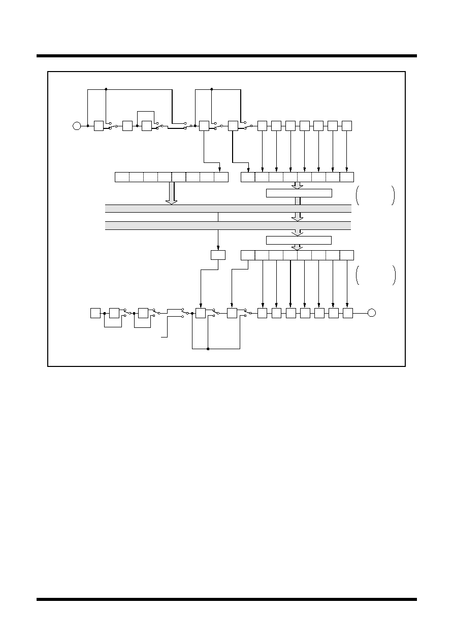
114
Tentative Specifications REV.A
Mitsubishi microcomputers
M16C / 62T Group
SINGLE-CHIP 16-BIT CMOS MICROCOMPUTER
S
pecifications in this manual are tentative and subject to change.
Under
development
Serial I/O
Figure 1.19.2. Block diagram of UARTi (i = 0, 1) transmit/receive unit
SP
SP
PAR
2SP
1SP
UART
UART (7 bits)
UART (8 bits)
UART (7 bits)
UART (9 bits)
Clock
synchronous
type
Clock synchronous
type
TxDi
UARTi transmit register
PAR
enabled
PAR
disabled
D
8
D
7
D
6
D
5
D
4
D
3
D
2
D
1
D
0
SP: Stop bit
PAR: Parity bit
UARTi transmit
buffer register
MSB/LSB conversion circuit
UART (8 bits)
UART (9 bits)
Clock synchronous
type
UARTi receive
buffer register
UARTi receive register
2SP
1SP
PAR
enabled
PAR
disabled
UART
UART (7 bits)
UART (9 bits)
Clock
synchronous
type
Clock
synchronous type
UART (7 bits)
UART (8 bits)
RxDi
Clock
synchronous type
UART (8 bits)
UART (9 bits)
Address 03A6
16
Address 03A7
16
Address 03AE
16
Address 03AF
16
Address 03A2
16
Address 03A3
16
Address 03AA
16
Address 03AB
16
Data bus low-order bits
MSB/LSB conversion circuit
D
7
D
6
D
5
D
4
D
3
D
2
D
1
D
0
D
8
0
0
0
0
0
0
0
SP
SP
PAR
"0"
Data bus high-order bits
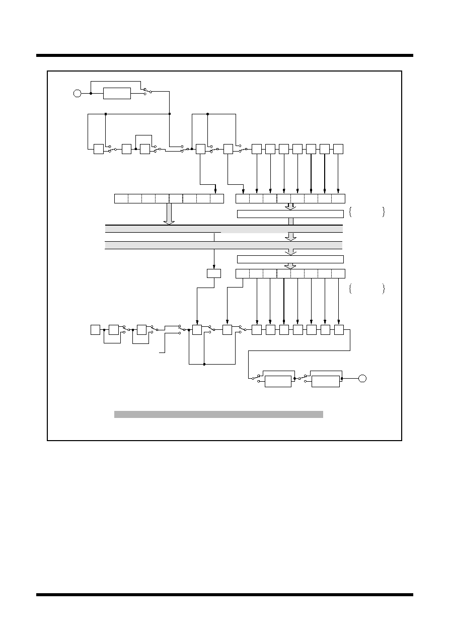
115
Tentative Specifications REV.A
Mitsubishi microcomputers
M16C / 62T Group
SINGLE-CHIP 16-BIT CMOS MICROCOMPUTER
S
pecifications in this manual are tentative and subject to change.
Under
development
Serial I/O
SP
SP
PAR
2SP
1SP
UART
UART
(7 bits)
UART
(8 bits)
UART(7 bits)
UART
(9 bits)
Clock
synchronous
type
Clock
synchronous type
Data bus low-order bits
TxD2
UART2 transmit register
PAR
disabled
PAR
enabled
D
8
D
7
D
6
D
5
D
4
D
3
D
2
D
1
D
0
UART2 transmit
buffer register
UART
(8 bits)
UART
(9 bits)
Clock
synchronous type
UART2 receive
buffer register
UART2 receive register
2SP
1SP
UART
(7 bits)
UART
(8 bits)
UART(7 bits)
UART
(9 bits)
Clock
synchronous type
Clock
synchronous type
RxD2
UART
(8 bits)
UART
(9 bits)
Address 037E
16
Address 037F
16
Address 037A
16
Address 037B
16
Data bus high-order bits
D
7
D
6
D
5
D
4
D
3
D
2
D
1
D
0
D
8
0
0
0
0
0
0
0
SP
SP
PAR
"0"
Reverse
No reverse
Error signal
output circuit
RxD data
reverse circuit
Error signal output
enable
Error signal output
disable
Reverse
No reverse
Logic reverse circuit + MSB/LSB conversion circuit
Logic reverse circuit + MSB/LSB conversion circuit
PAR
enabled
PAR
disabled
UART
Clock
synchronous
type
TxD data
reverse circuit
SP: Stop bit
PAR: Parity bit
Note 1: In M30623(80-pin package), do not use UART2 as clock synchronous serial I/O.
Figure 1.19.3. Block diagram of UART2 transmit/receive unit
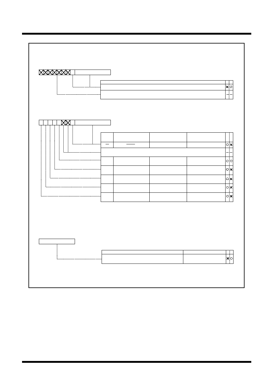
116
Tentative Specifications REV.A
Mitsubishi microcomputers
M16C / 62T Group
SINGLE-CHIP 16-BIT CMOS MICROCOMPUTER
S
pecifications in this manual are tentative and subject to change.
Under
development
Serial I/O
Figure 1.19.4. Serial I/O-related registers (1)
b7
UARTi bit rate generator
b0
Symbol
Address
When reset
U0BRG
03A1
16
Indeterminate
U1BRG
03A9
16
Indeterminate
U2BRG
0379
16
Indeterminate
Function
Assuming that set value = n, BRGi divides the count source by
n + 1
00
16
to FF
16
Values that can be set
W
R
b7
b0
(b15)
(b8)
b7
b0
UARTi transmit buffer register
Function
Transmit data
Nothing is assigned.
In an attempt to write to these bits, write "0". The value, if read, turn out to be indeterminate.
Symbol
Address
When reset
U0TB
03A3
16
, 03A2
16
Indeterminate
U1TB
03AB
16
, 03AA
16
Indeterminate
U2TB
037B
16
, 037A
16
Indeterminate
W
R
(b15)
Symbol
Address
When reset
U0RB
03A7
16
, 03A6
16
Indeterminate
U1RB
03AF
16
, 03AE
16
Indeterminate
U2RB
037F
16
, 037E
16
Indeterminate
b7
b0
(b8)
b7
b0
UARTi receive buffer register
Function
(During UART mode)
Function
(During clock synchronous
serial I/O mode)
Bit name
Bit
symbol
0 : No framing error
1 : Framing error found
0 : No parity error
1 : Parity error found
0 : No error
1 : Error found
Note 1: Bits 15 through 12 are set to "0" when the serial I/O mode select bit (bits 2 to 0 at addresses 03A0
16
,
03A8
16
and 0378
16
) are set to "000
2
" or the receive enable bit is set to "0".
(Bit 15 is set to "0" when bits 14 to 12 all are set to "0".) Bits 14 and 13 are also set to "0" when the
lower byte of the UARTi receive buffer register (addresses 03A6
16
, 03AE
16
and 037E
16
) is read out.
Note 2: Arbitration lost detecting flag is allocated to U2RB and noting but "0" may be written. Nothing is
assigned in bit 11 of U0RB and U1RB. These bits can neither be set or reset. When read, the value
of this bit is "0".
Invalid
Invalid
Invalid
OER
FER
PER
SUM
Overrun error flag (Note 1)
Framing error flag (Note 1)
Parity error flag (Note 1)
Error sum flag (Note 1)
0 : No overrun error
1 : Overrun error found
0 : No overrun error
1 : Overrun error found
Nothing is assigned.
In an attempt to write to these bits, write "0". The value, if read, turns out to be "0".
Receive data
W
R
Receive data
ABT
Arbitration lost detecting
flag (Note 2)
Invalid
0 : Not detected
1 : Detected
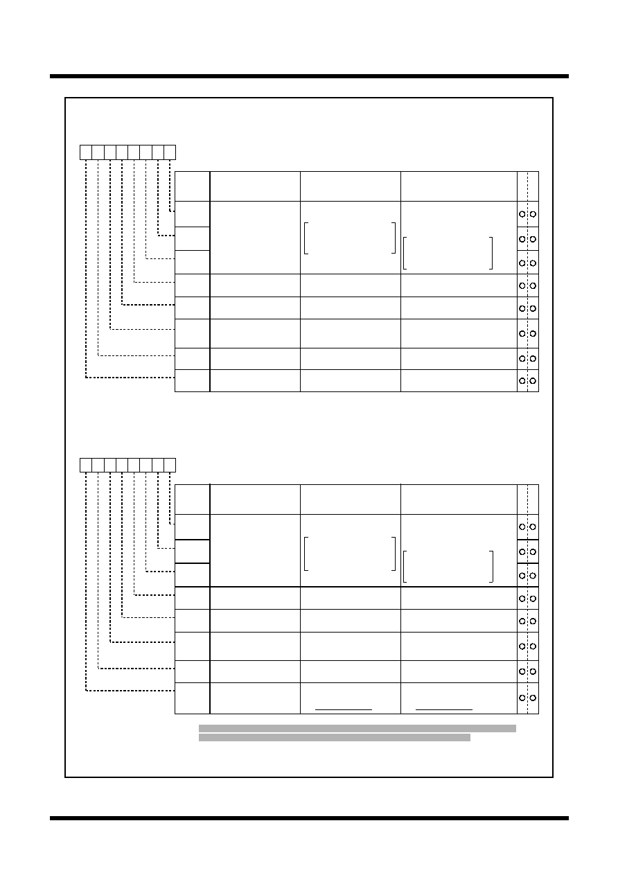
117
Tentative Specifications REV.A
Mitsubishi microcomputers
M16C / 62T Group
SINGLE-CHIP 16-BIT CMOS MICROCOMPUTER
S
pecifications in this manual are tentative and subject to change.
Under
development
Serial I/O
UARTi transmit/receive mode register
Symbol
Address
When reset
UiMR(i=0,1)
03A0
16
, 03A8
16
00
16
b7
b6
b5
b4
b3
b2
b1
b0
Bit name
Bit
symbol
W
R
Must be fixed to 001
0 0 0 : Serial I/O invalid
0 1 0 : Inhibited
0 1 1 : Inhibited
1 1 1 : Inhibited
b2 b1 b0
CKDIR
SMD1
SMD0
Serial I/O mode select bit
SMD2
Internal/external clock
select bit
STPS
PRY
PRYE
SLEP
Parity enable bit
0 : Internal clock
1 : External clock
Stop bit length select bit
Odd/even parity select bit
Sleep select bit
0 : One stop bit
1 : Two stop bits
0 : Parity disabled
1 : Parity enabled
0 : Sleep mode deselected
1 : Sleep mode selected
1 0 0 : Transfer data 7 bits long
1 0 1 : Transfer data 8 bits long
1 1 0 : Transfer data 9 bits long
0 0 0 : Serial I/O invalid
0 1 0 : Inhibited
0 1 1 : Inhibited
1 1 1 : Inhibited
b2 b1 b0
0 : Internal clock
1 : External clock
Invalid
Valid when bit 6 = "1"
0 : Odd parity
1 : Even parity
Invalid
Invalid
Must always be "0"
Function
(During UART mode)
Function
(During clock synchronous
serial I/O mode)
UART2 transmit/receive mode register
Symbol
Address
When reset
U2MR
0378
16
00
16
b7
b6
b5
b4
b3
b2
b1
b0
Bit name
Bit
symbol
W
R
Must be fixed to 001
0 0 0 : Serial I/O invalid
0 1 0 : (Note)
0 1 1 : Inhibited
1 1 1 : Inhibited
b2 b1 b0
CKDIR
SMD1
SMD0
Serial I/O mode select bit
SMD2
Internal/external clock
select bit
STPS
PRY
PRYE
IOPOL
Parity enable bit
0 : Internal clock
1 : External clock
Stop bit length select bit
Odd/even parity select bit
TxD, RxD I/O polarity
reverse bit
0 : One stop bit
1 : Two stop bits
0 : Parity disabled
1 : Parity enabled
0 : No reverse
1 : Reverse
Usually set to "0"
1 0 0 : Transfer data 7 bits long
1 0 1 : Transfer data 8 bits long
1 1 0 : Transfer data 9 bits long
0 0 0 : Serial I/O invalid
0 1 0 : Inhibited
0 1 1 : Inhibited
1 1 1 : Inhibited
b2 b1 b0
0 : Internal clock
1 : External clock
Invalid
Valid when bit 6 = "1"
0 : Odd parity
1 : Even parity
Invalid
Invalid
0 : No reverse
1 : Reverse
Usually set to "0"
Function
(During UART mode)
Function
(During clock synchronous
serial I/O mode)
Note 1: Bit 2 to bit 0 are set to "010
2
" when IIC mode is used.
Note 2: In M30623(80-pin package), do not select the external clock, because there is no external pin.
Note 3: In M30623(80-pin package), do not use UART2 as clock synchronous serial I/O.
(Note 3)
(Note 2)
Figure 1.19.5. Serial I/O-related registers (2)
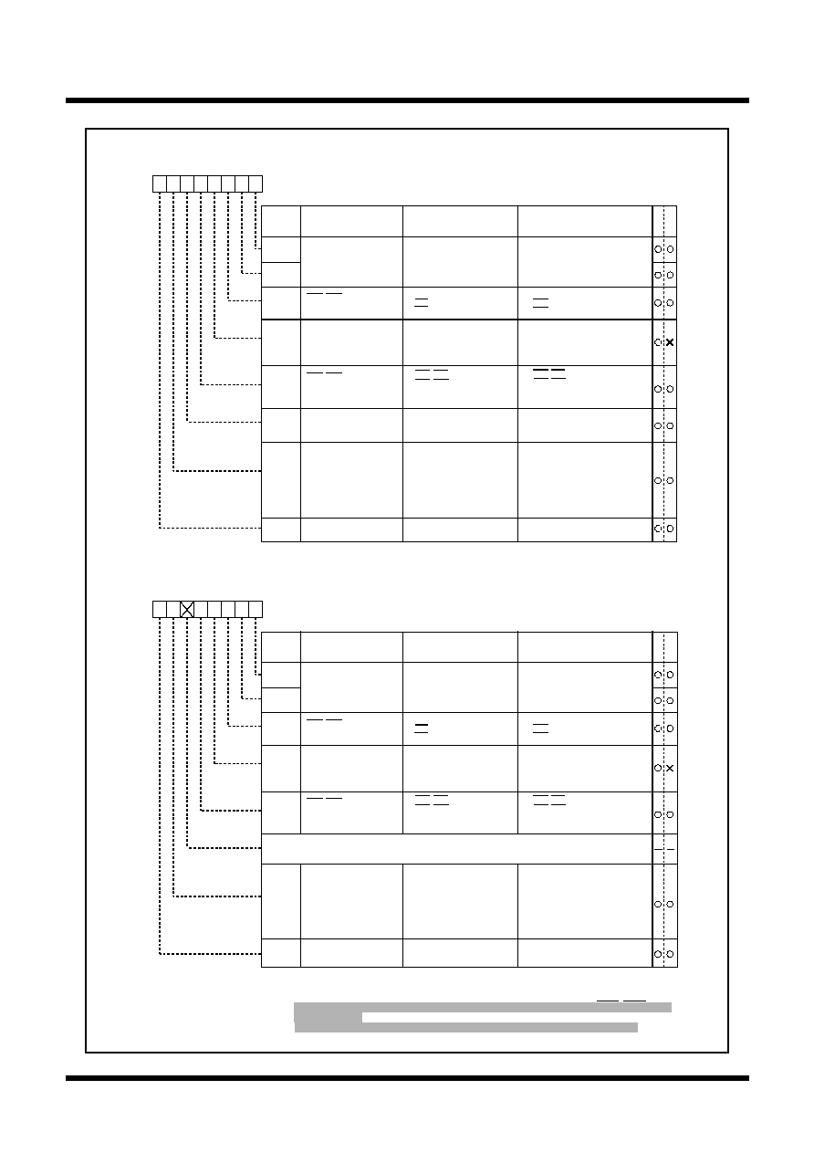
118
Tentative Specifications REV.A
Mitsubishi microcomputers
M16C / 62T Group
SINGLE-CHIP 16-BIT CMOS MICROCOMPUTER
S
pecifications in this manual are tentative and subject to change.
Under
development
Serial I/O
UARTi transmit/receive control register 0
Symbol
Address
When reset
UiC0(i=0,1)
03A4
16
, 03AC
16
08
16
b7
b6
b5
b4
b3
b2
b1
b0
Function
(During UART mode)
W
R
Function
(During clock synchronous
serial I/O mode)
TXEPT
CLK1
CLK0
CRS
CRD
NCH
CKPOL
BRG count source
select bit
Transmit register empty
flag
0 : Transmit data is output at
falling edge of transfer clock
and receive data is input at
rising edge
1 : Transmit data is output at
rising edge of transfer clock
and receive data is input at
falling edge
CLK polarity select bit
CTS/RTS function
select bit
CTS/RTS disable bit
Data output select bit
0 0 : f
1
is selected
0 1 : f
8
is selected
1 0 : f
32
is selected
1 1 : Inhibited
b1 b0
0 : LSB first
1 : MSB first
0 : Data present in transmit
register (during transmission)
1 : No data present in transmit
register (transmission
completed)
0 : CTS/RTS function enabled
1 : CTS/RTS function disabled
(P6
0
and P6
4
function as
programmable I/O port)
0 : TXDi pin is CMOS output
1 : TXDi pin is N-channel
open-drain output
UFORM Transfer format select bit
0 0 : f
1
is selected
0 1 : f
8
is selected
1 0 : f
32
is selected
1 1 : Inhibited
b1 b0
Valid when bit 4 = "0"
0 : CTS function is selected (Note 1)
1 : RTS function is selected (Note 2)
Valid when bit 4 = "0"
0 : CTS function is selected (Note 1)
1 : RTS function is selected (Note 2)
0 : Data present in transmit register
(during transmission)
1 : No data present in transmit
register (transmission completed)
0: TXDi pin is CMOS output
1: TXDi pin is N-channel
open-drain output
Must always be "0"
Bit name
Bit
symbol
Must always be "0"
Note 1: Set the corresponding port direction register to "0".
Note 2: The settings of the corresponding port register and port direction register are invalid.
0 : CTS/RTS function enabled
1 : CTS/RTS function disabled
(P6
0
and P6
4
function as
programmable I/O port)
UART2 transmit/receive control register 0
Symbol
Address
When reset
U2C0
037C
16
08
16
b7
b6
b5
b4
b3
b2
b1
b0
Function
(During UART mode)
W
R
Function
(During clock synchronous
serial I/O mode)
TXEPT
CLK1
CLK0
CRS
CRD
CKPOL
BRG count source
select bit
Transmit register empty
flag
0 : Transmit data is output at
falling edge of transfer clock
and receive data is input at
rising edge
1 : Transmit data is output at
rising edge of transfer clock
and receive data is input at
falling edge
CLK polarity select bit
CTS/RTS function
select bit
CTS/RTS disable bit
0 0 : f
1
is selected
0 1 : f
8
is selected
1 0 : f
32
is selected
1 1 : Inhibited
b1 b0
0 : LSB first
1 : MSB first
0 : Data present in transmit
register (during transmission)
1 : No data present in transmit
register (transmission
completed)
0 : CTS/RTS function enabled
1 : CTS/RTS function disabled
(P7
3
functions
programmable I/O port)
0 : TXDi pin is CMOS output
1 : TXDi pin is N-channel
open-drain output
UFORM Transfer format select bit
(Note 3)
0 0 : f
1
is selected
0 1 : f
8
is selected
1 0 : f
32
is selected
1 1 : Inhibited
b1 b0
Valid when bit 4 = "0"
0 : CTS function is selected (Note 1)
1 : RTS function is selected (Note 2)
Valid when bit 4 = "0"
0 : CTS function is selected (Note 1)
1 : RTS function is selected (Note 2)
0 : Data present in transmit register
(during transmission)
1 : No data present in transmit
register (transmission completed)
0: TXDi pin is CMOS output
1: TXDi pin is N-channel
open-drain output
Must always be "0"
Bit name
Bit
symbol
Note 1: Set the corresponding port direction register to "0".
Note 2: The settings of the corresponding port register and port direction register are invalid.
Note 3: Only clock synchronous serial I/O mode and 8-bit UART mode are valid.
Note 4: In M30623(80-pin package), these bits are invalid, because CLK
2
and CTS
2
/RTS
2
have
no external pin.
Note 5: In M30623(80-pin package), do not use UART2 as clock synchronous serial I/O.
0 : CTS/RTS function enabled
1 : CTS/RTS function disabled
(P7
3
functions programmable
I/O port)
Nothing is assigned.
In an attempt to write to this bit, write "0". The value, if read, turns out to be "0".
0 : LSB first
1 : MSB first
(Note 5)
(Note 4)
(Note 4)
(Note 4)
Figure 1.19.6. Serial I/O-related registers (3)
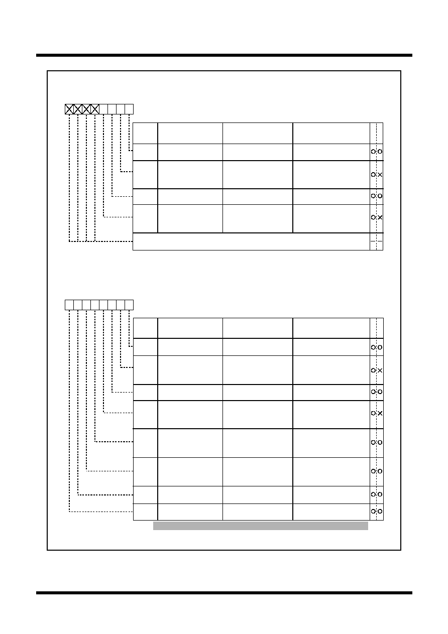
119
Tentative Specifications REV.A
Mitsubishi microcomputers
M16C / 62T Group
SINGLE-CHIP 16-BIT CMOS MICROCOMPUTER
S
pecifications in this manual are tentative and subject to change.
Under
development
Serial I/O
Figure 1.19.7. Serial I/O-related registers (4)
UARTi transmit/receive control register 1
Symbol
Address
When reset
UiC1(i=0,1)
03A5
16
,
03AD
16
02
16
b7
b6
b5
b4
b3
b2
b1
b0
Bit name
Bit
symbol
W
R
Function
(During UART mode)
Function
(During clock synchronous
serial I/O mode)
TE
TI
RE
RI
Transmit enable bit
Receive enable bit
Receive complete flag
Transmit buffer
empty flag
0 : Transmission disabled
1 : Transmission enabled
0 : Data present in
transmit buffer register
1 : No data present in
transmit buffer register
0 : Reception disabled
1 : Reception enabled
0 : Transmission disabled
1 : Transmission enabled
0 : Data present in
transmit buffer register
1 : No data present in
transmit buffer register
0 : Reception disabled
1 : Reception enabled
0 : No data present in
receive buffer register
1 : Data present in
receive buffer register
0 : No data present in
receive buffer register
1 : Data present in
receive buffer register
Nothing is assigned.
In an attempt to write to these bits, write "0". The value, if read, turns out to be "0".
UART2 transmit/receive control register 1
Symbol
Address
When reset
U2C1
037D
16
02
16
b7
b6
b5
b4
b3
b2
b1
b0
Bit name
Bit
symbol
W
R
Function
(During UART mode)
Function
(During clock synchronous
serial I/O mode)
TE
TI
RE
RI
Transmit enable bit
Receive enable bit
Receive complete flag
Transmit buffer
empty flag
0 : Transmission disabled
1 : Transmission enabled
0 : Data present in
transmit buffer register
1 : No data present in
transmit buffer register
0 : Reception disabled
1 : Reception enabled
0 : Transmission disabled
1 : Transmission enabled
0 : Data present in
transmit buffer register
1 : No data present in
transmit buffer register
0 : Reception disabled
1 : Reception enabled
0 : No data present in
receive buffer register
1 : Data present in
receive buffer register
0 : No data present in
receive buffer register
1 : Data present in
receive buffer register
U2IRS
UART2 transmit interrupt
cause select bit
0 : Transmit buffer empty
(TI = 1)
1 : Transmit is completed
(TXEPT = 1)
0 : Transmit buffer empty
(TI = 1)
1 : Transmit is completed
(TXEPT = 1)
U2RRM UART2 continuous
receive mode enable bit
0 : Continuous receive
mode disabled
1 : Continuous receive
mode enabled
Invalid
Data logic select bit
0 : No reverse
1 : Reverse
0 : No reverse
1 : Reverse
U2LCH
U2ERE Error signal output
enable bit
Must be fixed to "0"
0 : Output disabled
1 : Output enabled
Note 1: In M30623(80-pin package), do not use UART2 as clock synchronous serial I/O.
(Note 1)
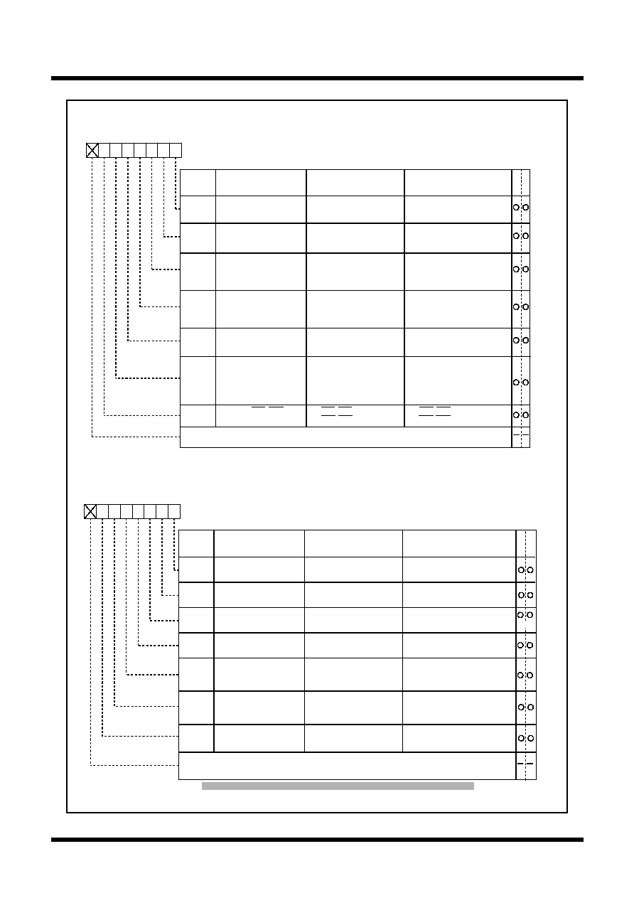
120
Tentative Specifications REV.A
Mitsubishi microcomputers
M16C / 62T Group
SINGLE-CHIP 16-BIT CMOS MICROCOMPUTER
S
pecifications in this manual are tentative and subject to change.
Under
development
Serial I/O
Note: When using multiple pins to output the transfer clock, the following requirements must be met:
· UART1 internal/external clock select bit (bit 3 at address 03A8
16
) = "0".
UART transmit/receive control register 2
Symbol
Address
When reset
UCON
03B0
16
X0000000
2
b7
b6
b5
b4
b3
b2
b1
b0
Bit
name
Bit
symbol
W
R
Function
(During UART mode)
Function
(During clock synchronous
serial I/O mode)
CLKMD0
CLKMD1
RCSP
UART0 transmit
interrupt cause select bit
UART0 continuous
receive mode enable bit
0 : Continuous receive
mode disabled
1 : Continuous receive
mode enable
UART1 continuous
receive mode enable bit
CLK/CLKS select bit 0
UART1 transmit
interrupt cause select bit
0 :
Transmit buffer empty (Tl = 1)
1 : Transmission completed
(TXEPT = 1)
0 :
Transmit buffer empty (Tl = 1)
1 : Transmission completed
(TXEPT = 1)
0 : Normal mode
(CLK output is CLK1 only)
1 : Transfer clock output
from multiple pins
function selected
0 : Continuous receive
mode disabled
1 : Continuous receive
mode enabled
Nothing is assigned.
In an attempt to write to this bit, write "0". The value, if read, turns out to be indeterminate.
0 : Transmit buffer empty (Tl = 1)
1 : Transmission completed
(TXEPT = 1)
0 : Transmit buffer empty (Tl = 1)
1 : Transmission completed
(TXEPT = 1)
Must always be "0"
U0IRS
U1IRS
U0RRM
U1RRM
0 : CTS/RTS shared pin
1 : CTS/RTS separated
0 : CTS/RTS shared pin
1 : CTS/RTS separated
Separate CTS/RTS bit
Invalid
Invalid
Invalid
CLK/CLKS select
bit 1 (Note)
Valid when bit 5 = "1"
0 : Clock output to CLK1
1 : Clock output to CLKS1
UART2 special mode register
Symbol
Address
When reset
U2SMR
0377
16
00
16
b7
b6
b5
b4 b3
b2
b1
b0
Bit
name
Bit
symbol
W
R
Function
(During UART mode)
Function
(During clock synchronous
serial I/O mode)
ABSCS
ACSE
SSS
IIC mode selection bit
Bus busy flag
0 : STOP condition detected
1 : START condition detected
SCLL sync output
enable bit
Bus collision detect
sampling
clock select bit
Arbitration lost detecting
flag control bit
0 : Normal mode
1 : IIC mode
0 : Update per bit
1 : Update per byte
IICM
ABC
BBS
LSYN
0 : Ordinary
1 : Falling edge of RxD2
0 : Disabled
1 : Enabled
Transmit start condition
select bit
Must always be "0"
0 : Rising edge of transfer
clock
1 : Underflow signal of timer A0
Auto clear function
select bit of transmit
enable bit
0 : No auto clear function
1 : Auto clear at occurrence of
bus collision
Must always be "0"
Must always be "0"
Must always be "0"
Must always be "0"
Must always be "0"
Must always be "0"
Nothing is assigned.
In an attempt to write to this bit, write "0". The value, if read, turns out to be "0".
(Note 2)
Note 1: In M30623(80-pin package), do not use UART2 as clock synchronous serial I/O.
Note 2: Nothing but "0" may be written.
(Note 1)
Figure 1.19.8. Serial I/O-related registers (5)
121
Tentative Specifications REV.A
Mitsubishi microcomputers
M16C / 62T Group
SINGLE-CHIP 16-BIT CMOS MICROCOMPUTER
S
pecifications in this manual are tentative and subject to change.
Under
development
Clock synchronous serial I/O mode
Item
Specification
Transfer data format
· Transfer data length: 8 bits
Transfer clock
· When internal clock is selected (bit 3 at addresses 03A0
16
, 03A8
16
, 0378
16
= "0") : fi/ 2(n+1)
(Note 1) fi = f
1
, f
8
, f
32
· When external clock is selected (bit 3 at addresses 03A0
16
, 03A8
16
, 0378
16
= "1") : Input from CLKi pin
Transmission/reception control
_______
_______
_______
_______
·
CTS
function/
RTS
function/
CTS
,
RTS
function chosen to be invalid
Transmission start condition
· To start transmission, the following requirements must be met:
_
Transmit enable bit (bit 0 at addresses 03A5
16
, 03AD
16
, 037D
16
) = "1"
_
Transmit buffer empty flag (bit 1 at addresses 03A5
16
, 03AD
16
, 037D
16
) = "0"
_______
_______
_
When CTS function selected, CTS input level = "L"
· Furthermore, if external clock is selected, the following requirements must also be met:
_
CLKi polarity select bit (bit 6 at addresses 03A4
16
, 03AC
16
, 037C
16
) = "0":
CLKi input level = "H"
_
CLKi polarity select bit (bit 6 at addresses 03A4
16
, 03AC
16
, 037C
16
) = "1":
CLKi input level = "L"
Reception start condition
· To start reception, the following requirements must be met:
_
Receive enable bit (bit 2 at addresses 03A5
16
, 03AD
16
, 037D
16
) = "1"
_
Transmit enable bit (bit 0 at addresses 03A5
16
, 03AD
16
, 037D
16
) = "1"
_
Transmit buffer empty flag (bit 1 at addresses 03A5
16
, 03AD
16
, 037D
16
) = "0"
· Furthermore, if external clock is selected, the following requirements must
also be met:
_
CLKi polarity select bit (bit 6 at addresses 03A4
16
, 03AC
16
, 037C
16
) = "0":
CLKi input level = "H"
_
CLKi polarity select bit (bit 6 at addresses 03A4
16
, 03AC
16
, 037C
16
) = "1":
CLKi input level = "L"
· When transmitting
_
Transmit interrupt cause select bit (bits 0, 1 at address 03B0
16
, bit 4 at
address 037D
16
) = "0": Interrupts requested when data transfer from UARTi
transfer buffer register to UARTi transmit register is completed
_
Transmit interrupt cause select bit (bits 0, 1 at address 03B0
16
, bit 4 at
address 037D
16
) = "1": Interrupts requested when data transmission from
UARTi transfer register is completed
· When receiving
_
Interrupts requested when data transfer from UARTi receive register to
UARTi receive buffer register is completed
Error detection
· Overrun error (Note 2)
This error occurs when the next data is ready before contents of UARTi
receive buffer register are read out
Interrupt request
generation timing
Note 1: "n" denotes the value 00
16
to FF
16
that is set to the UART bit rate generator.
Note 2: If an overrun error occurs, the UARTi receive buffer will have the next data written in. Note also that
the UARTi receive interrupt request bit is not set to "1".
(1) Clock synchronous serial I/O mode
The clock synchronous serial I/O mode uses a transfer clock to transmit and receive data. Tables 1.19.2
and 1.19.3 list the specifications of the clock synchronous serial I/O mode. Figure 1.19.9 shows the
UARTi transmit/receive mode register.
In M30623(80-pin package), do not use UART2 as clock synchronous serial I/O.
Table 1.19.2. Specifications of clock synchronous serial I/O mode (1)

122
Tentative Specifications REV.A
Mitsubishi microcomputers
M16C / 62T Group
SINGLE-CHIP 16-BIT CMOS MICROCOMPUTER
S
pecifications in this manual are tentative and subject to change.
Under
development
Clock synchronous serial I/O mode
Item
Specification
Select function
· CLK polarity selection
Whether transmit data is output/input at the rising edge or falling edge of the
transfer clock can be selected
· LSB first/MSB first selection
Whether transmission/reception begins with bit 0 or bit 7 can be selected
· Continuous receive mode selection
Reception is enabled simultaneously by a read from the receive buffer register
· Transfer clock output from multiple pins selection (UART1) (Note)
UART1 transfer clock can be chosen by software to be output from one of
the two pins set
_______ _______
· Separate CTS/RTS pins
(UART0) (Note)
_______
_______
UART0 CTS and RTS pins each can be assigned to separate pins
· Switching serial data logic (UART2)
Whether to reverse data in writing to the transmission buffer register or
reading the reception buffer register can be selected.
· TxD, RxD I/O polarity reverse (UART2)
This function is reversing TxD port output and RxD port input. All I/O data
level is reversed.
Table 1.19.4. Specifications of clock synchronous serial I/O mode (2)
_______ _______
Note: The transfer clock output from multiple pins and the separate CTS/RTS pins functions cannot be
selected simultaneously.

123
Tentative Specifications REV.A
Mitsubishi microcomputers
M16C / 62T Group
SINGLE-CHIP 16-BIT CMOS MICROCOMPUTER
S
pecifications in this manual are tentative and subject to change.
Under
development
Clock synchronous serial I/O mode
Figure 1.19.9. UARTi transmit/receive mode register in clock synchronous serial I/O mode
Symbol
Address
When reset
UiMR(i=0,1)
03A0
16
, 03A8
16
00
16
CKDIR
UARTi transmit/receive mode registers
Internal/external clock
select bit
STPS
PRY
PRYE
SLEP
0 : Internal clock
1 : External clock
Bit name
Function
Bit symbol
W
R
b7
b6
b5
b4
b3
b2
b1
b0
0 (Must always be "0" in clock synchronous serial I/O mode)
0 1
0
SMD0
SMD1
SMD2
Serial I/O mode select bit
0 0 1 : Clock synchronous serial
I/O mode
b2 b1 b0
0
Invalid in clock synchronous serial I/O mode
Symbol
Address
When reset
U2MR
0378
16
00
16
CKDIR
UART2 transmit/receive mode register
Internal/external clock
select bit
STPS
PRY
PRYE
IOPOL
0 : Internal clock
1 : External clock
Bit name
Function
Bit symbol
W
R
b7
b6
b5
b4
b3
b2
b1
b0
0 1
0
SMD0
SMD1
SMD2
Serial I/O mode select bit
0 0 1 : Clock synchronous serial
I/O mode
b2 b1 b0
0
Invalid in clock synchronous serial I/O mode
TxD, RxD I/O polarity
reverse bit (Note)
0 : No reverse
1 : Reverse
Note: Usually set to "0".
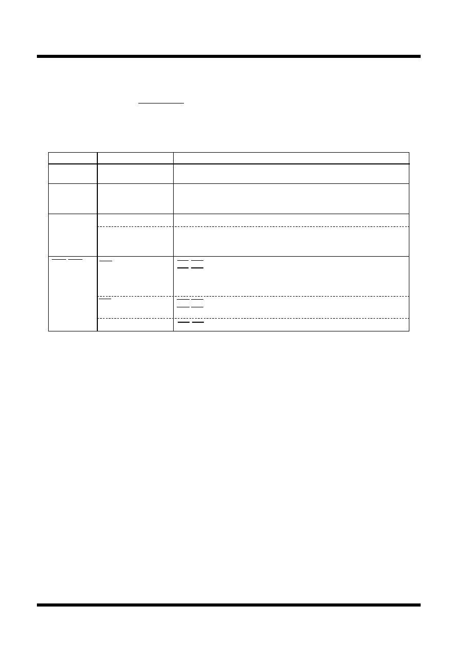
124
Tentative Specifications REV.A
Mitsubishi microcomputers
M16C / 62T Group
SINGLE-CHIP 16-BIT CMOS MICROCOMPUTER
S
pecifications in this manual are tentative and subject to change.
Under
development
Clock synchronous serial I/O mode
Table 1.19.4 lists the functions of the input/output pins during clock synchronous serial I/O mode. This
_______
table shows the pin functions when the transfer clock output from multiple pins and the separate CTS/
_______
RTS pins functions are not selected. Note that for a period from when the UARTi operation mode is
selected to when transfer starts, the TxDi pin outputs a "H". (If the N-channel open-drain is selected, this
pin is in floating state.)
Table 1.19.4. Input/output pin functions in clock synchronous serial I/O mode
Pin name
Function
Method of selection
TxDi
(P6
3
, P6
7
, P7
0
)
Serial data output
Serial data input
Transfer clock output
Transfer clock input
Programmable I/O port
(Outputs dummy data when performing reception only)
RxDi
(P6
2
, P6
6
, P7
1
)
CLKi
(P6
1
, P6
5
, P7
2
)
Internal/external clock select bit (bit 3 at address 03A0
16
, 03A8
16
, 0378
16
) = "0"
Internal/external clock select bit (bit 3 at address 03A0
16
, 03A8
16
, 0378
16
) = "1"
Port P6
1
, P6
5
and P7
2
direction register (bits 1 and 5 at address 03EE
16
,
bit 2 at address 03EF
16
) = "0"
Port P6
2
, P6
6
and P7
1
direction register (bits 2 and 6 at address 03EE
16
,
bit 1 at address 03EF
16
)= "0"
(Can be used as an input port when performing transmission only)
CTS/RTS disable bit (bit 4 at address 03A4
16
, 03AC
16
, 037C
16
) ="0"
CTS/RTS function select bit (bit 2 at address 03A4
16
, 03AC
16
, 037C
16
) = "0"
Port P6
0
, P6
4
and P7
3
direction register (bits 0 and 4 at address 03EE
16
,
bit 3 at address 03EF
16
) = "0"
CTS/RTS disable bit (bit 4 at address 03A4
16
, 03AC
16
, 037C
16)
= "0"
CTS/RTS function select bit (bit 2 at address 03A4
16
, 03AC
16
, 037C
16
) = "1"
CTS/RTS disable bit (bit 4 at address 03A4
16
, 03AC
16
, 037C
16
) = "1"
CTS input
RTS output
CTSi/RTSi
(P6
0
, P6
4
, P7
3
)
_______ _______
(when transfer clock output from multiple pins and separate CTS/RTS pins functions are not selected)
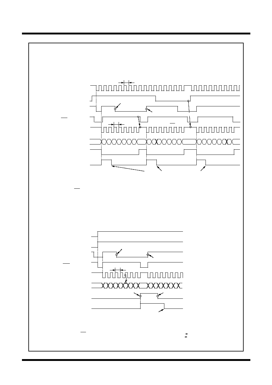
125
Tentative Specifications REV.A
Mitsubishi microcomputers
M16C / 62T Group
SINGLE-CHIP 16-BIT CMOS MICROCOMPUTER
S
pecifications in this manual are tentative and subject to change.
Under
development
Clock synchronous serial I/O mode
Figure 1.19.10. Typical transmit/receive timings in clock synchronous serial I/O mode
· Example of transmit timing (when internal clock is selected)
D
0
D
1
D
2
D
3
D
4
D
5
D
6
D
7
D
0
D
1
D
2
D
3
D
4
D
5
D
6
D
7
D
0
D
1
D
2
D
3
D
4
D
5
D
6
D
7
Tc
T
CLK
Stopped pulsing because transfer enable bit = "0"
Data is set in UARTi transmit buffer register
Tc = TCLK = 2(n + 1) / fi
fi: frequency of BRGi count source (f
1
, f
8
, f
32
)
n: value set to BRGi
Transfer clock
Transmit enable
bit (TE)
Transmit buffer
empty flag (Tl)
CLKi
TxDi
Transmit
register empty
flag (TXEPT)
"H"
"L"
"0"
"1"
"0"
"1"
"0"
"1"
CTSi
The above timing applies to the following settings:
· Internal clock is selected.
· CTS function is selected.
· CLK polarity select bit = "0".
· Transmit interrupt cause select bit = "0"
Transmit interrupt
request bit (IR)
"0"
"1"
Stopped pulsing because CTS = "H"
Transferred from UARTi transmit buffer register to UARTi transmit register
Shown in ( ) are bit symbols.
Cleared to "0" when interrupt request is accepted, or cleared by software
1 / f
EXT
Dummy data is set in UARTi transmit buffer register
Transmit enable
bit (TE)
Transmit buffer
empty flag (Tl)
CLKi
RxDi
Receive complete
flag (Rl)
RTSi
"H"
"L"
"0"
"1"
"0"
"1"
"0"
"1"
Receive enable
bit (RE)
"0"
"1"
Receive data is taken in
Transferred from UARTi transmit buffer register to UARTi transmit register
Read out from UARTi receive buffer register
The above timing applies to the following settings:
· External clock is selected.
· RTS function is selected.
· CLK polarity select bit = "0".
f
EXT
: frequency of external clock
Transferred from UARTi receive register
to UARTi receive buffer register
Receive interrupt
request bit (IR)
"0"
"1"
D
0
D
1
D
2
D
3
D
4
D
5
D
6
D
7
D
0
D
1
D
2
D
3
D
4
D
5
Shown in ( ) are bit symbols.
Cleared to "0" when interrupt request is accepted, or cleared by software
Meet the following conditions are met when the CLK
input before data reception = "H"
· Transmit enable bit "1"
· Receive enable bit "1"
· Dummy data write to UARTi transmit buffer register
· Example of receive timing (when external clock is selected)
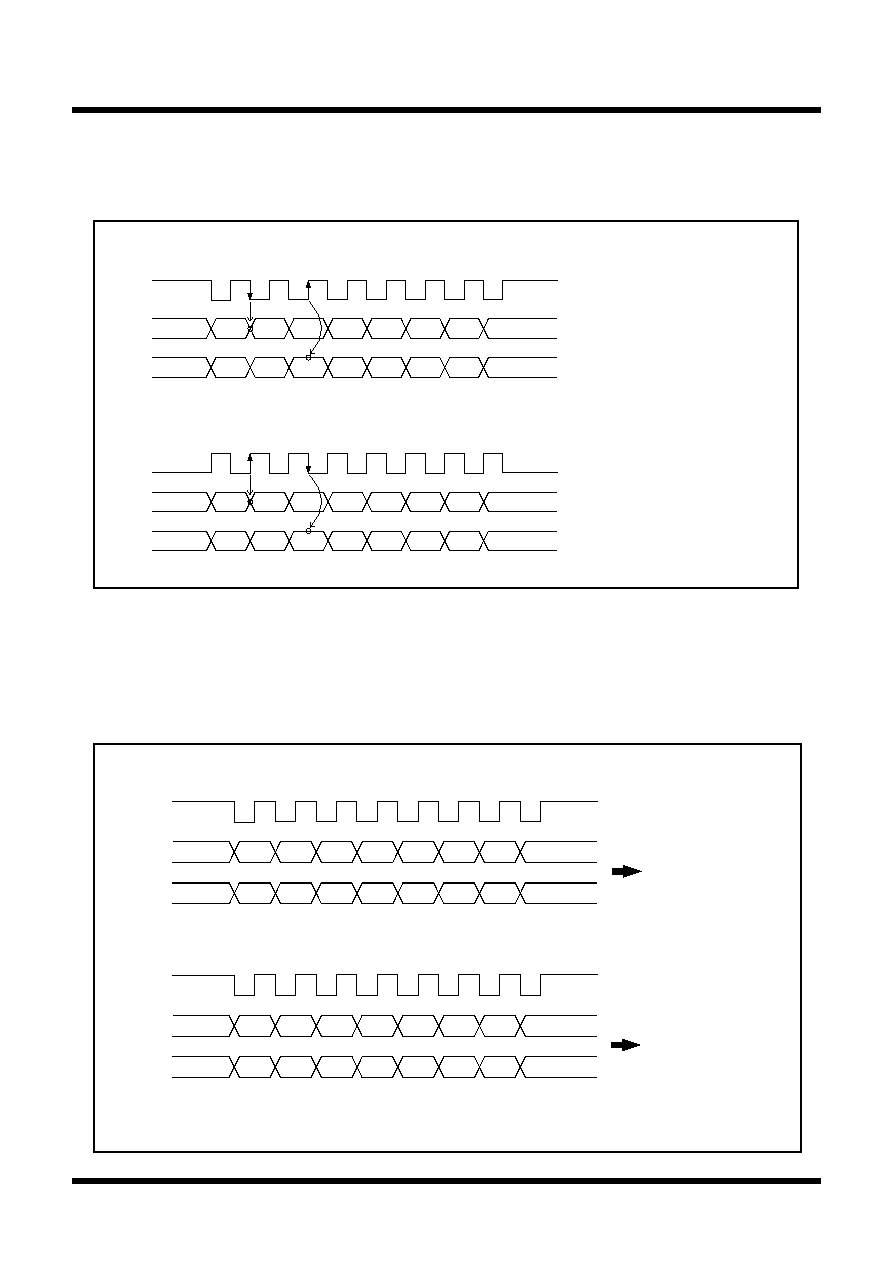
126
Tentative Specifications REV.A
Mitsubishi microcomputers
M16C / 62T Group
SINGLE-CHIP 16-BIT CMOS MICROCOMPUTER
S
pecifications in this manual are tentative and subject to change.
Under
development
Clock synchronous serial I/O mode
(a) Polarity select function
As shown in Figure 1.19.11, the CLK polarity select bit (bit 6 at addresses 03A4
16
, 03AC
16
, 037C
16
)
allows selection of the polarity of the transfer clock.
· When CLK polarity select bit = "1"
Note 2: The CLK pin level when not
transferring data is "L".
D
1
D
2
D
3
D
4
D
5
D
6
D
7
D
1
D
2
D
3
D
4
D
5
D
6
D
7
D
0
D
0
T
X
D
i
R
X
D
i
CLK
i
· When CLK polarity select bit = "0"
Note 1: The CLK pin level when not
transferring data is "H".
D
1
D
2
D
3
D
4
D
5
D
6
D
7
D0
D
1
D
2
D
3
D
4
D
5
D
6
D
7
D
0
T
X
D
i
R
X
D
i
CLK
i
Figure 1.19.11. Polarity of transfer clock
(b) LSB first/MSB first select function
As shown in Figure 1.19.12, when the transfer format select bit (bit 7 at addresses 03A4
16
, 03AC
16
,
037C
16
) = "0", the transfer format is "LSB first"; when the bit = "1", the transfer format is "MSB first".
Figure 1.19.12. Transfer format
LSB first
· When transfer format select bit = "0"
D0
D
0
D
1
D
2
D
3
D
4
D
5
D
6
D
7
D
1
D
2
D
3
D
4
D
5
D
6
D
7
T
X
D
i
R
X
D
i
CLK
i
· When transfer format select bit = "1"
D
6
D
5
D
4
D
3
D
2
D
1
D
0
D
7
D
7
D
6
D
5
D
4
D
3
D
2
D
1
D
0
T
X
D
i
R
X
D
i
CLK
i
MSB first
Note: This applies when the CLK polarity select bit = "0".
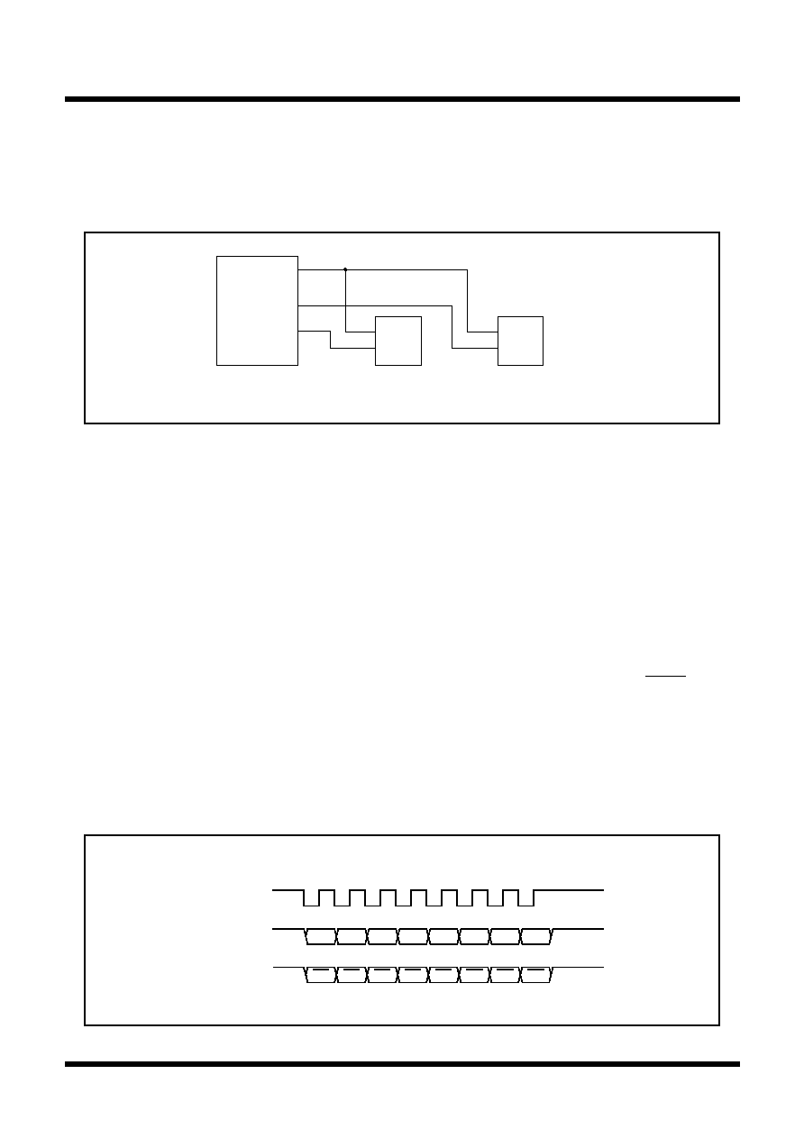
127
Tentative Specifications REV.A
Mitsubishi microcomputers
M16C / 62T Group
SINGLE-CHIP 16-BIT CMOS MICROCOMPUTER
S
pecifications in this manual are tentative and subject to change.
Under
development
Clock synchronous serial I/O mode
(c) Transfer clock output from multiple pins function (UART1)
This function allows the setting two transfer clock output pins and choosing one of the two to output a
clock by using the CLK and CLKS select bit (bits 4 and 5 at address 03B0
16
). (See Figure 1.19.3.)
The multiple pins function is valid only when the internal clock is selected for UART1. Note that when
_______ _______
this function is selected, UART1 CTS/RTS function cannot be used.
Figure 1.19.13. The transfer clock output from the multiple pins function usage
Microcomputer
T
X
D
1
(P6
7
)
CLKS
1
(P6
4
)
CLK
1
(P6
5
)
IN
CLK
IN
CLK
Note: This applies when the internal clock is selected and transmission
is performed only in clock synchronous serial I/O mode.
(d) Continuous receive mode
If the continuous receive mode enable bit (bits 2 and 3 at address 03B0
16
, bit 5 at address 037D
16
) is
set to "1", the unit is placed in continuous receive mode. In this mode, when the receive buffer register
is read out, the unit simultaneously goes to a receive enable state without having to set dummy data to
the transmit buffer register back again.
_______ _______
(e) Separate CTS/RTS pins function (UART0)
This function works the same way as in the clock asynchronous serial I/O (UART) mode. The method
of setting and the input/output pin functions are both the same, so refer to select function in the next
section, "(2) Clock asynchronous serial I/O (UART) mode." Note that this function is invalid if the
transfer clock output from the multiple pins function is selected.
(f) Serial data logic switch function (UART2)
When the data logic select bit (bit6 at address 037D
16
) = "1", and writing to transmit buffer register or
reading from receive buffer register, data is reversed. Figure 1.19.14 shows the example of serial data
logic switch timing.
Figure 1.19.14. Serial data logic switch timing
D0
D1
D2
D3
D4
D5
D6
D7
D0
D1
D2
D3
D4
D5
D6
D7
Transfer clock
TxD
2
(no reverse)
TxD
2
(reverse)
"H"
"L"
"H"
"L"
"H"
"L"
·When LSB first
128
Tentative Specifications REV.A
Mitsubishi microcomputers
M16C / 62T Group
SINGLE-CHIP 16-BIT CMOS MICROCOMPUTER
S
pecifications in this manual are tentative and subject to change.
Under
development
Clock asynchronous serial I/O (UART) mode
Item
Specification
Transfer data format
· Character bit (transfer data): 7 bits, 8 bits, or 9 bits as selected
· Start bit: 1 bit
· Parity bit: Odd, even, or nothing as selected
· Stop bit: 1 bit or 2 bits as selected
Transfer clock
· When internal clock is selected (bit 3 at addresses 03A0
16
, 03A8
16
, 0378
16
= "0") :
fi/16(n+1) (Note 1)
fi = f
1
, f
8
, f
32
· When external clock is selected (bit 3 at addresses 03A0
16
, 03A8
16
, 0378
16
="1") :
f
EXT
/16(n+1) (Note 1) (Note 2)
Transmission/reception control
_______
_______
_______
_______
· CTS function/RTS function/CTS, RTS function chosen to be invalid (Note 4)
Transmission start condition
· To start transmission, the following requirements must be met:
- Transmit enable bit (bit 0 at addresses 03A5
16
, 03AD
16
, 037D
16
) = "1"
- Transmit buffer empty flag (bit 1 at addresses 03A5
16
, 03AD
16
, 037D
16
) = "0"
_______
_______
- When CTS function selected, CTS input level = "L" (Note 4)
Reception start condition
· To start reception, the following requirements must be met:
- Receive enable bit (bit 2 at addresses 03A5
16
, 03AD
16
, 037D
16
) = "1"
- Start bit detection
Interrupt request
· When transmitting
generation timing
-
T
ransmit interrupt cause select bits (bits 0,1 at address 03B0
16
, bit4 at
address 037D
16
) = "0": Interrupts requested when data transfer from UARTi
transfer buffer register to UARTi transmit register is completed
- Transmit interrupt cause select bits (bits 0, 1 at address 03B0
16
, bit4 at
address 037D
16
) = "1": Interrupts requested when data transmission from
UARTi transfer register is completed
·
When receiving
- Interrupts requested when data transfer from UARTi receive register to
UARTi receive buffer register is completed
Error detection
· Overrun error (Note 3)
This error occurs when the next data is ready before contents of UARTi
receive buffer register are read out
· Framing error
This error occurs when the number of stop bits set is not detected
· Parity error
This error occurs when if parity is enabled, the number of 1's in parity and
character bits does not match the number of 1's set
· Error sum flag
This flag is set (= 1) when any of the overrun, framing, and parity errors is
encountered
(2) Clock asynchronous serial I/O (UART) mode
The UART mode allows transmitting and receiving data after setting the desired transfer rate and transfer
data format. Tables 1.19.5 and 1.19.6 list the specifications of the UART mode. Figure 1.19.15 shows
the UARTi transmit/receive mode register.
Table 1.19.5. Specifications of UART Mode (1)
Note 1: `n' denotes the value 00
16
to FF
16
that is set to the UARTi bit rate generator.
Note 2: f
EXT
is input from the CLKi pin. In M30623(80-pin package), do not select the external clock as transfer clock,
because there is no external pin of CLK
2
.
Note 3: If an overrun error occurs, the UARTi receive buffer will have the next data written in. Note also that
the UARTi receive interrupt request bit is not set to "1".
________
________
Note 4: In M30623(80-pin package), do not use these functions, because there is no external pin of CTS
2
/RTS
2
.

129
Tentative Specifications REV.A
Mitsubishi microcomputers
M16C / 62T Group
SINGLE-CHIP 16-BIT CMOS MICROCOMPUTER
S
pecifications in this manual are tentative and subject to change.
Under
development
Clock asynchronous serial I/O (UART) mode
Table 1.19.6. Specifications of UART Mode (2)
Item
Specification
Select function
_______ _______
· Separate CTS/RTS pins (UART0)
_______
_______
UART0 CTS and RTS pins each can be assigned to separate pins
· Sleep mode selection (UART0, UART1)
This mode is used to transfer data to and from one of multiple slave micro-
computers
· Serial data logic switch (UART2)
This function is reversing logic value of transferring data. Start bit, parity bit
and stop bit are not reversed.
· T
X
D, R
X
D I/O polarity switch
This function is reversing T
X
D port output and R
X
D port input. All I/O data
level is reversed.
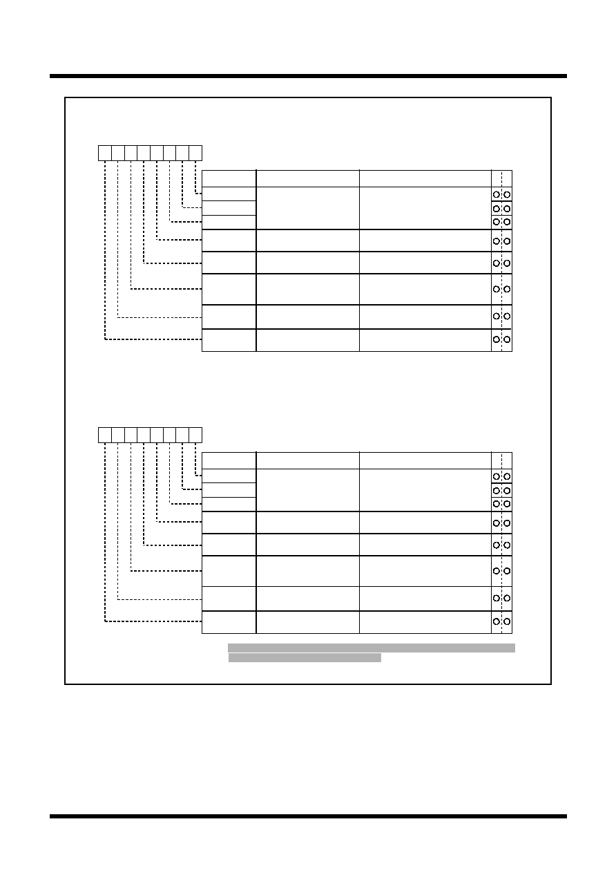
130
Tentative Specifications REV.A
Mitsubishi microcomputers
M16C / 62T Group
SINGLE-CHIP 16-BIT CMOS MICROCOMPUTER
S
pecifications in this manual are tentative and subject to change.
Under
development
Clock asynchronous serial I/O (UART) mode
Figure 1.19.15. UARTi transmit/receive mode register in UART mode
Symbol
Address
When reset
UiMR(i=0,1)
03A0
16
, 03A8
16
00
16
CKDIR
UARTi transmit / receive mode registers
Internal / external clock
select bit
STPS
PRY
PRYE
SLEP
0 : Internal clock
1 : External clock
Bit name
Function
Bit symbol
W
R
b7
b6
b5
b4
b3
b2
b1
b0
SMD0
SMD1
SMD2
Serial I/O mode select bit
b2 b1 b0
0 : One stop bit
1 : Two stop bits
0 : Parity disabled
1 : Parity enabled
0 : Sleep mode deselected
1 : Sleep mode selected
1 0 0 : Transfer data 7 bits long
1 0 1 : Transfer data 8 bits long
1 1 0 : Transfer data 9 bits long
Valid when bit 6 = "1"
0 : Odd parity
1 : Even parity
Stop bit length select bit
Odd / even parity
select bit
Parity enable bit
Sleep select bit
Symbol
Address
When reset
U2MR
0378
16
00
16
CKDIR
UART2 transmit / receive mode register
Internal / external clock
select bit
STPS
PRY
PRYE
IOPOL
0 : Internal clock
1 : External clock (Note 2)
Bit name
Function
Bit symbol
W
R
b7
b6
b5
b4
b3
b2
b1
b0
SMD0
SMD1
SMD2
Serial I/O mode select bit
b2 b1 b0
0 : One stop bit
1 : Two stop bits
0 : Parity disabled
1 : Parity enabled
0 : No reverse
1 : Reverse
1 0 0 : Transfer data 7 bits long
1 0 1 : Transfer data 8 bits long
1 1 0 : Transfer data 9 bits long
Valid when bit 6 = "1"
0 : Odd parity
1 : Even parity
Stop bit length select bit
Odd / even parity
select bit
Parity enable bit
TxD, RxD I/O polarity
reverse bit (Note 1)
Note 1: Usually set to "0".
Note 2: In M30623(80-pin package), do not select the external clock as transfer clock,
because there is no external pin of CLK
2
.
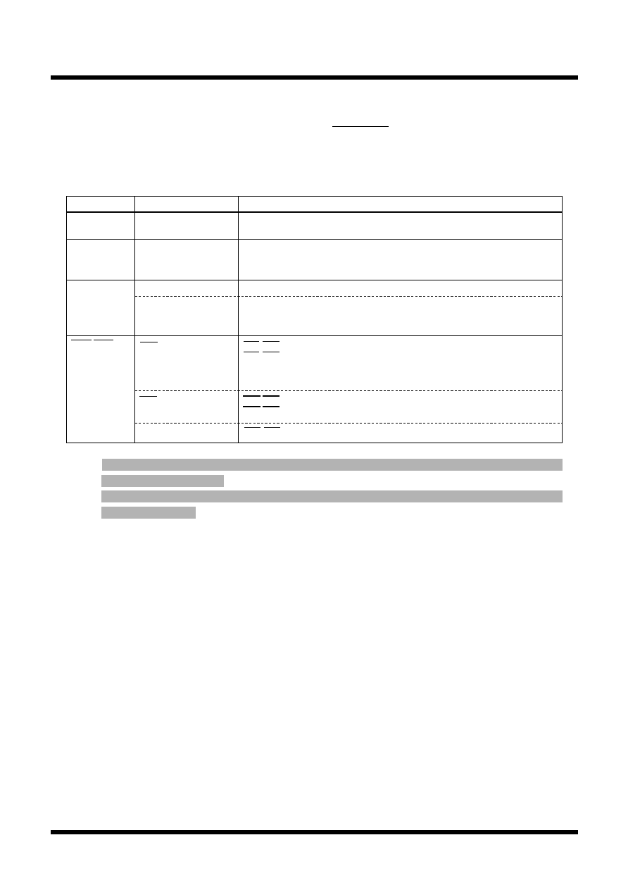
131
Tentative Specifications REV.A
Mitsubishi microcomputers
M16C / 62T Group
SINGLE-CHIP 16-BIT CMOS MICROCOMPUTER
S
pecifications in this manual are tentative and subject to change.
Under
development
Clock asynchronous serial I/O (UART) mode
Table 1.19.7 lists the functions of the input/output pins during UART mode. This table shows the pin
_______ _______
functions when the separate CTS/RTS pins function is not selected. Note that for a period from when the
UARTi operation mode is selected to when transfer starts, the TxDi pin outputs a "H". (If the N-channel
open-drain is selected, this pin is in floating state.)
Table 1.19.7. Input/output pin functions in UART mode
Pin name
Function
Method of selection
TxDi
(P6
3
, P6
7
, P7
0
)
Serial data output
Serial data input
Programmable I/O port
Transfer clock input
Programmable I/O port
RxDi
(P6
2
, P6
6
, P7
1
)
CLKi
(P6
1
, P6
5
, P7
2
)
Internal/external clock select bit (bit 3 at address 03A0
16
, 03A8
16
, 0378
16
) = "0"
Internal/external clock select bit (bit 3 at address 03A0
16
, 03A8
16
, 0378
16
) = "1"
Port P6
1
, P6
5
and P7
2
direction register (bits 1 and 5 at address 03EE
16
,
bit 2 at address 03EF
16
) = "0"
Port P6
2
, P6
6
and P7
1
direction register (bits 2 and 6 at address 03EE
16
,
bit 1 at address 03EF
16
)= "0"
(Can be used as an input port when performing transmission only)
CTS/RTS disable bit (bit 4 at address 03A4
16
, 03AC
16
, 037C
16
) ="0"
CTS/RTS function select bit (bit 2 at address 03A4
16
, 03AC
16
, 037C
16
) = "0"
Port P6
0
, P6
4
and P7
3
direction register (bits 0 and 4 at address 03EE
16
,
bit 3 at address 03EF
16
) = "0"
CTS/RTS disable bit (bit 4 at address 03A4
16
, 03AC
16
, 037C
16)
= "0"
CTS/RTS function select bit (bit 2 at address 03A4
16
, 03AC
16
, 037C
16
) = "1"
CTS/RTS disable bit (bit 4 at address 03A4
16
, 03AC
16
, 037C
16
) = "1"
CTS input
RTS output
CTSi/RTSi
(P6
0
, P6
4
, P7
3
)
(Note 1)
(Note 2)
________ _______
(when separate CTS/RTS pins function is not selected)
Note 1: In M30623(80-pin package), use the internal clock as transfer clock of UART2, because there is no
external pin of CLK
2
(P7
2
).
Note 2: In M30623(80-pin package), UART2 does not have these functions, because there is no external pin
________
_______
of CTS
2
/RTS
2
(P7
3
).
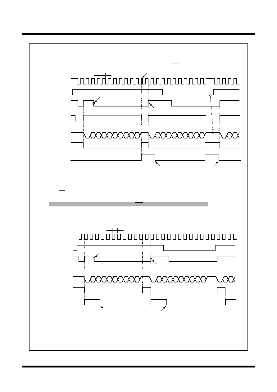
132
Tentative Specifications REV.A
Mitsubishi microcomputers
M16C / 62T Group
SINGLE-CHIP 16-BIT CMOS MICROCOMPUTER
S
pecifications in this manual are tentative and subject to change.
Under
development
Clock asynchronous serial I/O (UART) mode
Transmit enable
bit(TE)
Transmit buffer
empty flag(TI)
Transmit register
empty flag (TXEPT)
Start
bit
Parity
bit
TxDi
CTSi
The above timing applies to the following settings :
· Parity is enabled.
· One stop bit.
· CTS function is selected.
· Transmit interrupt cause select bit = "1".
"1"
"0"
"1"
"L"
"H"
"0"
"1"
Tc = 16 (n + 1) / fi or 16 (n + 1) / f
EXT
fi : frequency of BRGi count source (f
1
, f
8
, f
32
)
f
EXT
: frequency of BRGi count source (external clock)
n : value set to BRGi
Transmit interrupt
request bit (IR)
"0"
"1"
Cleared to "0" when interrupt request is accepted, or cleared by software
Transmit enable
bit(TE)
Transmit buffer
empty flag(TI)
TxDi
Transmit register
empty flag (TXEPT)
"0"
"1"
"0"
"1"
"0"
"1"
The above timing applies to the following settings :
· Parity is disabled.
· Two stop bits.
· CTS function is disabled.
· Transmit interrupt cause select bit = "0".
Transfer clock
Tc
Tc = 16 (n + 1) / fi or 16 (n + 1) / f
EXT
fi : frequency of BRGi count source (f
1
, f
8
, f
32
)
f
EXT
: frequency of BRGi count source (external clock)
n : value set to BRGi
Transmit interrupt
request bit (IR)
"0"
"1"
Shown in ( ) are bit symbols.
Shown in ( ) are bit symbols.
Tc
Transfer clock
D
0
D
1
D
2
D
3
D
4
D
5
D
6
D
7
ST
P
D
0
D
1
D
2
D
3
D
4
D
5
D
6
D
7
SP
ST
P
SP
D
0
D
1
ST
Stopped pulsing because transmit enable bit = "0"
Stop
bit
Transferred from UARTi transmit buffer register to UARTi transmit register
Start
bit
The transfer clock stops momentarily as CTS is "H" when the stop bit is checked.
The transfer clock starts as the transfer starts immediately CTS changes to "L".
Data is set in UARTi transmit buffer register
D
0
D
1
D
2
D
3
D
4
D
5
D
6
D
7
ST
SP
D
8
D
0
D
1
D
2
D
3
D
4
D
5
D
6
D
7
ST
D
8
D
0
D
1
ST
SPSP
Transferred from UARTi transmit buffer register to UARTi transmit register
Stop
bit
Stop
bit
Data is set in UARTi transmit buffer register.
"0"
SP
Cleared to "0" when interrupt request is accepted, or cleared by software
Note 1: In M30623(80-pin package), there is no external pin of CTS
2
, so do not use the function using this pin.
· Example of transmit timing when transfer data is 8 bits long (parity enabled, one stop bit)
· Example of transmit timing when transfer data is 9 bits long (parity disabled, two stop bits)
Figure 1.19.16. Typical transmit timings in UART mode
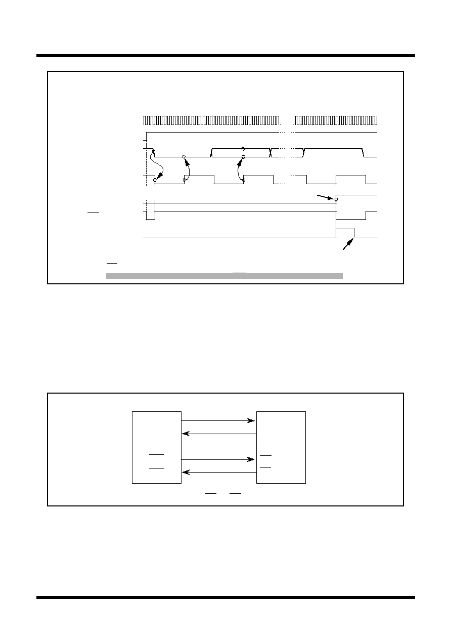
133
Tentative Specifications REV.A
Mitsubishi microcomputers
M16C / 62T Group
SINGLE-CHIP 16-BIT CMOS MICROCOMPUTER
S
pecifications in this manual are tentative and subject to change.
Under
development
Clock asynchronous serial I/O (UART) mode
· Example of receive timing when transfer data is 8 bits long (parity disabled, one stop bit)
Figure 1.19.17. Typical receive timing in UART mode
_______ _______
(a) Separate CTS/RTS pins function (UART0)
_______ _______
_______
Setting the CTS/RTS separate bit (bit 6 of address 03B0
16
) to "1" inputs/outputs the CTS signal and
_______
_______
_______
_______ _______
RTS signal from different pins. Choose which to use, CTS or RTS, by use of the CTS/RTS function
select bit (bit 2 of address 03A4
16
). This function is effective in UART0 only. With this function cho-
_______ _______
_______ _______
sen, the user cannot use the CTS/RTS function. Set "0" both to the CTS/RTS function select bit (bit
_______ _______
2 of address 03AC
16
) and to the CTS/RTS disable bit (bit 4 of address 03AC
16
).
(b) Sleep mode (UART0, UART1)
This mode is used to transfer data between specific microcomputers among multiple microcomputers
connected using UARTi. The sleep mode is selected when the sleep select bit (bit 7 at addresses
03A0
16
, 03A8
16
) is set to "1" during reception. In this mode, the unit performs receive operation when
the MSB of the received data = "1" and does not perform receive operation when the MSB = "0".
D
0
Start bit
Sampled "L"
Receive data taken in
BRGi count
source
Receive enable bit
RxDi
Transfer clock
Receive
complete flag
RTSi
Stop bit
"1"
"0"
"0"
"1"
"H"
"L"
The above timing applies to the following settings :
·Parity is disabled.
·One stop bit.
·RTS function is selected.
Receive interrupt
request bit
"0"
"1"
Transferred from UARTi receive register to
UARTi receive buffer register
Reception triggered when transfer clock
is generated by falling edge of start bit
D
7
D
1
Cleared to "0" when interrupt request is accepted, or cleared by software
Note 1: In M30623(80-pin package), there is no external pin of RTS
2
, so do not use the function using this pin.
_______ _______
Figure 1.19.18. The separate CTS/RTS pins function usage
Microcomputer
T
X
D
0
(P6
3
)
R
X
D
0
(P6
2
)
IN
OUT
CTS
RTS
CTS0 (P6
4
)
RTS0 (P6
0
)
IC
Note : The user cannot use CTS and RTS at the same time.
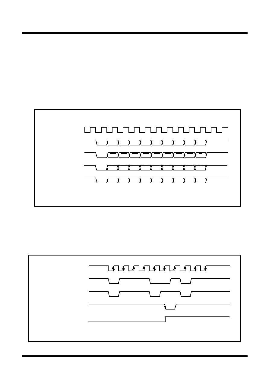
134
Tentative Specifications REV.A
Mitsubishi microcomputers
M16C / 62T Group
SINGLE-CHIP 16-BIT CMOS MICROCOMPUTER
S
pecifications in this manual are tentative and subject to change.
Under
development
Clock asynchronous serial I/O (UART) mode
(c) Function for switching serial data logic (UART2)
When the data logic select bit (bit 6 of address 037D
16
) is assigned 1, data is inverted in writing to the
transmission buffer register or reading the reception buffer register. Figure 1.19.19 shows the ex-
ample of timing for switching serial data logic.
Figure 1.19.19. Timing for switching serial data logic, and I/O polarity reverse
ST : Start bit
P : Even parity
SP : Stop bit
Transfer clock
"H"
"L"
D0
D1
D2
D3
D4
D5
D6
D7
P
SP
ST
"H"
"L"
SP
ST
D3
D4
D5
D6
D7
P
D0
D1
D2
"H"
"L"
· When LSB first, parity enabled, one stop bit
No logic reverse
No polarity reverse
TxD
2
Logic reverse
No polarity reverse
TxD
2
Logic reverse
Polarity reverse
TxD
2
No logic reverse
Polarity reverse
TxD
2
SP
ST
D3
D4
D5
D6
D7
P
D0
D1
D2
"H"
"L"
D0
D1
D2
D3
D4
D5
D6
D7
P
SP
ST
"H"
"L"
(d) TxD, RxD I/O polarity reverse function (UART2)
This function is to reverse T
X
D pin output and R
X
D pin input. The level of any data to be input or output
(including the start bit, stop bit(s), and parity bit) is reversed. Set this function to "0" (not to reverse) for
usual use. Figure 1.19.19 shows the example of timing for I/O polarity reverse.
(e) Bus collision detection function (UART2)
This function is to sample the output level of the T
X
D pin and the input level of the R
X
D pin at the rising
edge of the transfer clock; if their values are different, then an interrupt request occurs. Figure 1.19.20
shows the example of detection timing of a buss collision (in UART mode).
Figure 1.19.20. Detection timing of a bus collision (in UART mode)
ST : Start bit
SP : Stop bit
ST
ST
SP
SP
Transfer clock
TxD
2
RxD
2
Bus collision detection
interrupt request signal
"H"
"L"
"H"
"L"
"H"
"L"
"1"
"0"
Bus collision detection
interrupt request bit
"1"
"0"
135
Tentative Specifications REV.A
Mitsubishi microcomputers
M16C / 62T Group
SINGLE-CHIP 16-BIT CMOS MICROCOMPUTER
S
pecifications in this manual are tentative and subject to change.
Under
development
Clock asynchronous serial I/O (UART) mode
Item
Specification
Transfer data format
· Transfer data 8-bit UART mode (bit 2 through bit 0 of address 0378
16
= "101
2
")
· One stop bit (bit 4 of address 0378
16
= "0")
· With the direct format chosen
Set parity to "even" (bit 5 and bit 6 of address 0378
16
= "1" and "1" respectively)
Set data logic to "direct" (bit 6 of address 037D
16
= "0").
Set transfer format to LSB (bit 7 of address 037C
16
= "0").
· With the inverse format chosen
Set parity to "odd" (bit 5 and bit 6 of address 0378
16
= "0" and "1" respectively)
Set data logic to "inverse" (bit 6 of address 037D
16
= "1")
Set transfer format to MSB (bit 7 of address 037C
16
= "1")
Transfer clock
· With the internal clock chosen (bit 3 of address 0378
16
= "0") : fi / 16 (n + 1) (Note 1) : fi=f
1
, f
8
, f
32
· With an external clock chosen (bit 3 of address 0378
16
= "1") : f
EXT
/ 16 (n+1) (Note 1) (Note 2)
Transmission / reception control
_______
_______
· Disable the CTS and RTS function (bit 4 of address 037C
16
= "1")
Other settings
· The sleep mode select function is not available for UART2
· Set transmission interrupt factor to "transmission completed" (bit 4 of address 037D
16
= "1")
Transmission start condition · To start transmission, the following requirements must be met:
- Transmit enable bit (bit 0 of address 037D
16
) = "1"
- Transmit buffer empty flag (bit 1 of address 037D
16
) = "0"
Reception start condition
· To start reception, the following requirements must be met:
- Reception enable bit (bit 2 of address 037D
16
) = "1"
- Detection of a start bit
· When transmitting
When data transmission from the UART2 transfer register is completed
(bit 4 of address 037D
16
= "1")
· When receiving
When data transfer from the UART2 receive register to the UART2 receive
buffer register is completed
Error detection
· Overrun error (see the specifications of clock-asynchronous serial I/O) (Note 3)
· Framing error (see the specifications of clock-asynchronous serial I/O)
· Parity error (see the specifications of clock-asynchronous serial I/O)
- On the reception side, an "L" level is output from the T
X
D
2
pin by use of the parity error
signal output function (bit 7 of address 037D
16
= "1") when a parity error is detected
- On the transmission side, a parity error is detected by the level of input to
the R
X
D
2
pin when a transmission interrupt occurs
· The error sum flag (see the specifications of clock-asynchronous serial I/O)
(3) Clock-asynchronous serial I/O mode (compliant with the SIM interface)
The SIM interface is used for connecting the microcomputer with a memory card or the like; adding some
extra settings in UART2 clock-asynchronous serial I/O mode allows the user to effect this function. Table
1.19.8 shows the specifications of clock-asynchronous serial I/O mode (compliant with the SIM interface).
Interrupt request
generation timing
Note 1: `n' denotes the value 00
16
to FF
16
that is set to the UARTi bit rate generator.
Note 2: f
EXT
is input from the CLK
2
pin. In M30623(80-pin package), do not select the external clock as transfer clock of
UART2, because there is no external pin of CLK
2
.
Note 3: If an overrun error occurs, the UART2 receive buffer will have the next data written in. Note also that the UARTi
receive interrupt request bit is not set to "1".
Table 1.19.8. Specifications of clock-asynchronous serial I/O mode (compliant with the SIM interface)
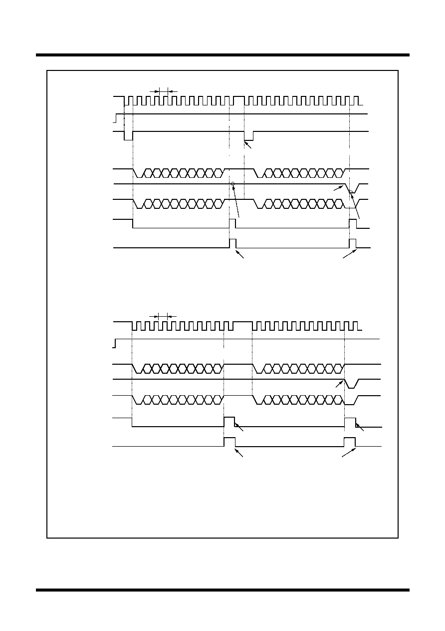
136
Tentative Specifications REV.A
Mitsubishi microcomputers
M16C / 62T Group
SINGLE-CHIP 16-BIT CMOS MICROCOMPUTER
S
pecifications in this manual are tentative and subject to change.
Under
development
Clock asynchronous serial I/O (UART) mode
Figure 1.19.21. Typical transmit/receive timing in UART mode (compliant with the SIM interface)
Transmit enable
bit(TE)
Transmit buffer
empty flag(TI)
Transmit register
empty flag (TXEPT)
D
0
D
1
D
2
D
3
D
4
D
5
D
6
D
7
ST
P
Start
bit
Parity
bit
The above timing applies to the following settings :
· Parity is enabled.
· One stop bit.
· Transmit interrupt cause select bit = "1".
"0"
"1"
"0"
"1"
"0"
"1"
Tc = 16 (n + 1) / fi or 16 (n + 1) / f
EXT
fi : frequency of BRGi count source (f
1
, f
8
, f
32
)
f
EXT
: frequency of BRGi count source (external clock)
n : value set to BRGi
Transmit interrupt
request bit (IR)
"0"
"1"
D
0
D
1
D
2
D
3
D
4
D
5
D
6
D
7
ST
P
Shown in ( ) are bit symbols.
Tc
Transfer clock
SP
Stop
bit
Data is set in UARTi transmit buffer register
SP
A "L" level returns from TxD
2
due to
the occurrence of a parity error.
The level is detected by the
interrupt routine.
The level is
detected by the
interrupt routine.
Receive enable
bit (RE)
Receive complete
flag (RI)
D
0
D
1
D
2
D
3
D
4
D
5
D
6
D
7
ST
P
Start
bit
Parity
bit
TxD
2
The above timing applies to the following settings :
· Parity is enabled.
· One stop bit.
· Transmit interrupt cause select bit = "0".
"0"
"1"
"0"
"1"
Tc = 16 (n + 1) / fi or 16 (n + 1) / f
EXT
fi : frequency of BRGi count source (f
1
, f
8
, f
32
)
f
EXT
: frequency of BRGi count source (external clock)
n : value set to BRGi
Receive interrupt
request bit (IR)
"0"
"1"
D
0
D
1
D
2
D
3
D
4
D
5
D
6
D
7
ST
P
SP
Shown in ( ) are bit symbols.
Tc
Transfer clock
SP
Stop
bit
A "L" level returns from TxD
2
due to
the occurrence of a parity error.
RxD
2
Read to receive buffer
Read to receive buffer
D
0
D
1
D
2
D
3
D
4
D
5
D
6
D
7
ST
P
Signal conductor level
(Note 1)
D
0
D
1
D
2
D
3
D
4
D
5
D
6
D
7
ST
P
SP
SP
D
0
D
1
D
2
D
3
D
4
D
5
D
6
D
7
ST
P
D
0
D
1
D
2
D
3
D
4
D
5
D
6
D
7
ST
P
SP
SP
TxD
2
RxD
2
Signal conductor level
(Note 1)
Note: Equal in waveform because TxD
2
and RxD
2
are connected.
Transferred from UARTi transmit buffer register to UARTi transmit register
Cleared to "0" when interrupt request is accepted, or cleared by software
Cleared to "0" when interrupt request is accepted, or cleared by software
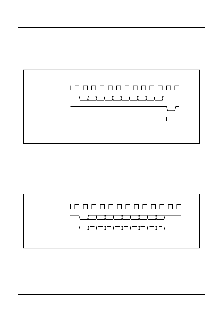
137
Tentative Specifications REV.A
Mitsubishi microcomputers
M16C / 62T Group
SINGLE-CHIP 16-BIT CMOS MICROCOMPUTER
S
pecifications in this manual are tentative and subject to change.
Under
development
Clock asynchronous serial I/O (UART) mode
(a) Function for outputting a parity error signal
With the error signal output enable bit (bit 7 of address 037D
16
) assigned "1", you can output an "L"
level from the TxD
2
pin when a parity error is detected. In step with this function, the generation timing
of a transmission completion interrupt changes to the detection timing of a parity error signal. Figure
1.19.22 shows the output timing of the parity error signal.
Figure 1.19.22. Output timing of the parity error signal
ST : Start bit
P : Even Parity
SP : Stop bit
D0
D1
D2
D3
D4
D5
D6
D7
P
SP
ST
Hi-Z
Transfer
clock
RxD
2
TxD
2
Receive
complete flag
"H"
"L"
"H"
"L"
"H"
"L"
"1"
· LSB first
"0"
(b) Direct format/inverse format
Connecting the SIM card allows you to switch between direct format and inverse format. If you choose
the direct format, D
0
data is output from TxD
2
. If you choose the inverse format, D
7
data is inverted
and output from TxD
2
.
Figure 1.19.23 shows the SIM interface format.
Figure 1.19.23. SIM interface format
P : Even parity
D0
D1
D2
D3
D4
D5
D6
D7
P
Transfer
clcck
TxD
2
(direct)
TxD
2
(inverse)
D7
D6
D5
D4
D3
D2
D1
D0
P
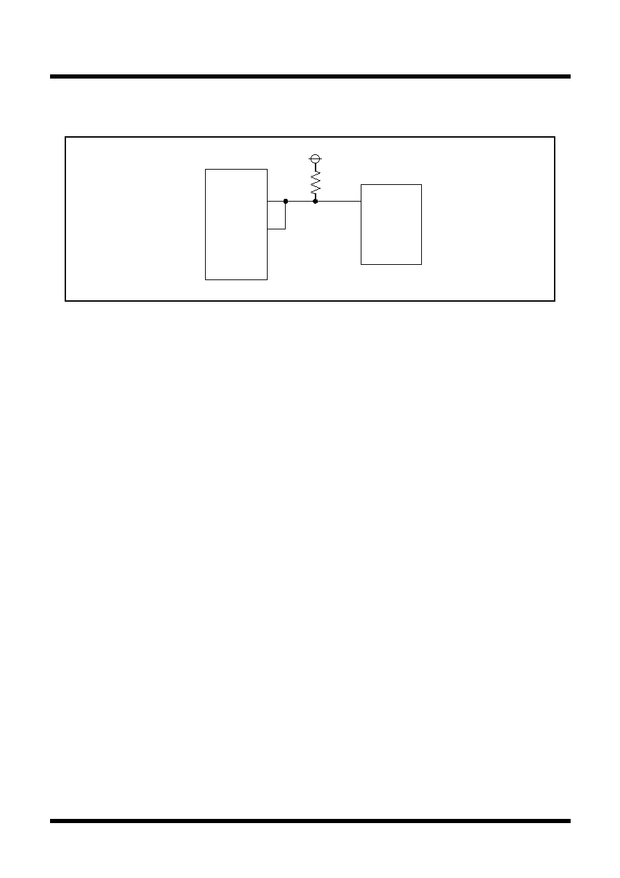
138
Tentative Specifications REV.A
Mitsubishi microcomputers
M16C / 62T Group
SINGLE-CHIP 16-BIT CMOS MICROCOMPUTER
S
pecifications in this manual are tentative and subject to change.
Under
development
Clock asynchronous serial I/O (UART) mode
Figure 1.19.24 shows the example of connecting the SIM interface. Connect T
X
D
2
and R
X
D
2
and apply
pull-up.
Figure 1.19.24. Connecting the SIM interface
Microcomputer
SIM card
TxD
2
RxD
2
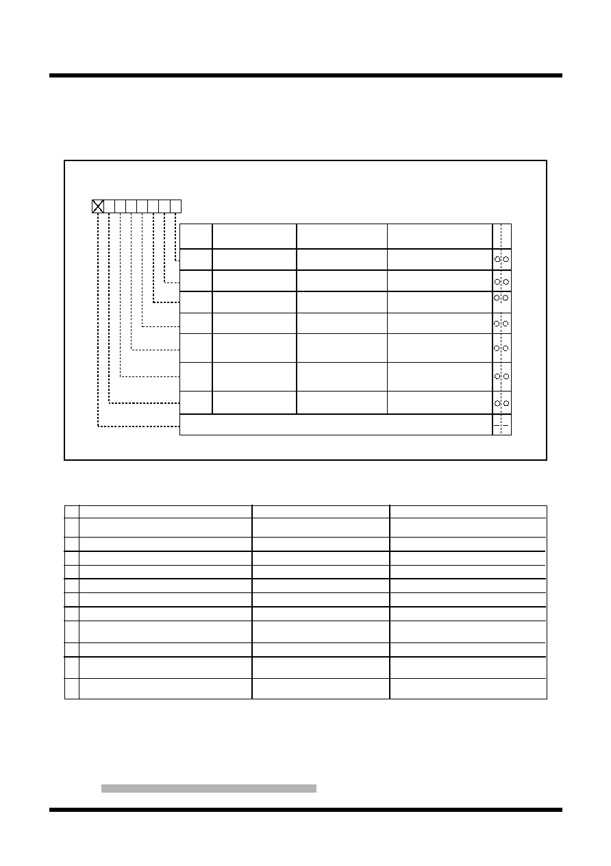
139
Tentative Specifications REV.A
Mitsubishi microcomputers
M16C / 62T Group
SINGLE-CHIP 16-BIT CMOS MICROCOMPUTER
S
pecifications in this manual are tentative and subject to change.
Under
development
UART2 Special Mode Register
UART2 Special Mode Register
The UART2 special mode register (address 0377
16
) is used to control UART2 in various ways.
Figure 1.19.25 shows the UART2 special mode register.
UART2 special mode register
Symbol
Address
When reset
U2SMR
0377
16
00
16
b7
b6 b5
b4
b3
b2
b1
b0
Bit name
Bit
symbol
W
R
Function
(During UART mode)
Function
(During clock synchronous
serial I/O mode)
ABSCS
ACSE
SSS
IIC mode selection bit
Bus busy flag
0 : STOP condition detected
1 : START condition detected
SCLL sync output
enable bit
Bus collision detect
sampling clock select bit
Arbitration lost detecting
flag control bit
0 : Normal mode
1 : IIC mode
0 : Update per bit
1 : Update per byte
IICM
ABC
BBS
LSYN
0 : Ordinary
1 : Falling edge of RxD2
0 : Disabled
1 : Enabled
Transmit start condition
select bit
Must always be "0"
0 : Rising edge of transfer
clock
1 : Underflow signal of timer A0
Auto clear function
select bit of transmit
enable bit
0 : No auto clear function
1 : Auto clear at occurrence of
bus collision
Must always be "0"
Must always be "0"
Must always be "0"
Must always be "0"
Must always be "0"
Must always be "0"
Nothing is assigned.
In an attempt to write to this bit, write "0". The value, if read, turns out to be "0".
Note: Nothing but "0" may be written.
(Note)
Figure 1.19.25. UART2 special mode register
Function
Normal mode
IIC mode (Note 1)
Factor of interrupt number 15 (Note 2)
UART2 transmission
No acknowledgment detection (NACK)
Factor of interrupt number 16 (Note 2)
UART2 reception
Start condition detection or stop
condition detection
UART2 transmission output delay
Not delayed
Delayed
P7
0
at the time when UART2 is in use
TxD
2
(output)
SDA (input/output) (Note 3)
P7
1
at the time when UART2 is in use
RxD
2
(input)
SCL (input/output)
P7
2
at the time when UART2 is in use
(Note 4)
CLK
2
P7
2
DMA1 factor at the time when 1 1 0 1 is assigned
to the DMA request factor selection bits
UART2 reception
Acknowledgment detection (ACK)
Noise filter width
15ns
50ns
Reading P7
1
Reading the terminal when 0 is
assigned to the direction register
Reading the terminal regardless of the
value of the direction register
1
2
3
4
5
6
7
8
9
Note 1: Make the settings given below when IIC mode is in use.
Set 0 1 0 in bits 2, 1, 0 of the UART2 transmission/reception mode register.
Disable the RTS/CTS function. Choose the LSB First function.
Note 2: Follow the steps given below to switch from a factor to another.
1. Disable the interrupt of the corresponding number.
2. Switch from a factor to another.
3. Reset the interrupt request flag of the corresponding number.
4. Set an interrupt level of the corresponding number.
Note 3: Set an initial value of SDA transmission output when serial I/O is invalid.
Note 4: In M30623(80-pin package), P7
2
is not connected to external pin.
Factor of interrupt number 10 (Note 2)
Bus collision detection
Acknowledgment detection (ACK)
10
Initial value of UART2 output
H level (when 0 is assigned to
the CLK polarity select bit)
The value set in latch P7
0
when the port is
selected
11
Table 1.19.9. Features in IIC mode
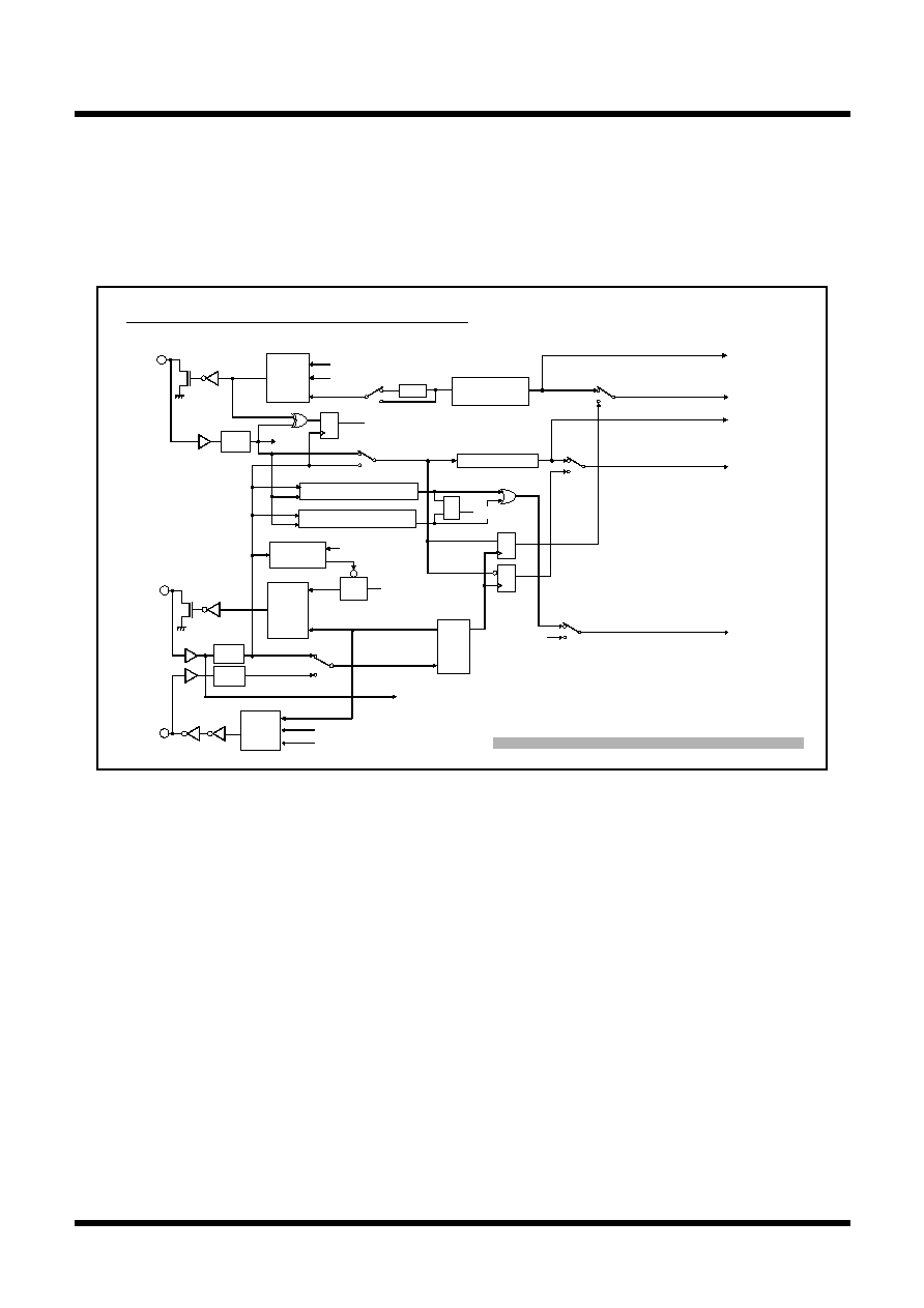
140
Tentative Specifications REV.A
Mitsubishi microcomputers
M16C / 62T Group
SINGLE-CHIP 16-BIT CMOS MICROCOMPUTER
S
pecifications in this manual are tentative and subject to change.
Under
development
UART2 Special Mode Register
Figure 1.19.26 shows the functional block diagram for IIC mode. Setting "1" in the IIC mode selection bit
(IICM) causes ports P7
0
, P7
1
, and P7
2
to work as data transmission-reception terminal SDA, clock input-
output terminal SCL, and port P7
2
respectively. A delay circuit is added to the SDA transmission output,
so the SDA output changes after SCL fully goes to "L". An attempt to read Port P7
1
(SCL) results in
getting the terminal's level regardless of the content of the port direction register. The initial value of SDA
transmission output in this mode goes to the value set in port P7
0
. The interrupt factors of the bus collision
detection interrupt, UART2 transmission interrupt, and of UART2 reception interrupt turn to the start/stop
condition detection interrupt, acknowledgment non-detection interrupt, and acknowledgment detection
interrupt respectively.
The start condition detection interrupt refers to the interrupt that occurs when the falling edge of the SDA
terminal (P7
0
) is detected with the SCL terminal (P7
1
) staying "H". The stop condition detection interrupt
refers to the interrupt that occurs when the rising edge of the SDA terminal (P7
0
) is detected with the SCL
terminal (P7
1
) staying "H". The bus busy flag (bit 2 of the UART2 special mode register) is set to "1" by the
start condition detection, and set to "0" by the stop condition detection.
In the first place, the control bits related to the IIC bus(simplified IIC bus) interface are explained.
Bit 0 of the UART special mode register (0377
16
) is used as the IIC mode selection bit.
Setting "1" in the IIC mode select bit (bit 0) goes the circuit to achieve the IIC bus interface effective.
Table 1.19.9 shows the relation between the IIC mode select bit and respective control workings.
Since this function uses clock-synchronous serial I/O mode, set this bit to "0" in UART mode.
P7
0
through P7
2
conforming to the simplified IIC bus
Selector
I/O
Timer
delay
Noize
Filter
Timer
UART2
Selector
(Port P7
1
output data latch)
I/O
P7
0
/TxD
2
/SDA
P7
1
/RxD
2
/SCL
Reception register
CLK
Internal clock
UART2
External clock
Selector
UART2
I/O
Timer
P7
2
/CLK
2
Arbitration
Start condition detection
Stop condition detection
Data bus
Falling edge
detection
D
T
Q
D
T
Q
D
T
Q
NACK
ACK
UART2
UART2
UART2
R
UART2 transmission/
NACK interrupt
request
UART2 reception/ACK
interrupt request
DMA1 request
9th pulse
IICM=1
IICM=0
IICM=1
IICM=0
IICM=1
IICM=0
IICM=0
IICM=1
IICM=0
IICM=1
IICM=1
IICM=0
Port reading
*
With IICM set to 1, the port terminal is to be readable
even if 1 is assigned to P7
1
of the direction register.
L-synchronous
output enabling bit
S
R Q
Bus busy
IICM=1
IICM=0
Bus collision/start, stop
condition detection
interrupt request
Bus collision
detection
Noize
Filter
Transmission
register
To DMA0, DMA1
Q
Noize
Filter
To DMA0
Note 1: In M30623(80-pin package), P7
2
/CLK
2
is not connected to external pin.
Figure 1.19.26. Functional block diagram for IIC mode

141
Tentative Specifications REV.A
Mitsubishi microcomputers
M16C / 62T Group
SINGLE-CHIP 16-BIT CMOS MICROCOMPUTER
S
pecifications in this manual are tentative and subject to change.
Under
development
UART2 Special Mode Register
The acknowledgment non-detection interrupt refers to the interrupt that occurs when the SDA terminal
level is detected still staying "H" at the rising edge of the 9th transmission clock. The acknowledgment
detection interrupt refers to the interrupt that occurs when SDA terminal's level is detected already went
to "L" at the 9th transmission clock. Also, assigning 1 1 0 1 (UART2 reception) to the DMA1 request factor
select bits provides the means to start up the DMA transfer by the effect of acknowledgment detection.
Bit 1 of the UART2 special mode register (0377
16
) is used as the arbitration loss detecting flag control bit.
Arbitration means the act of detecting the nonconformity between transmission data and SDA terminal
data at the timing of the SCL rising edge. This detecting flag is located at bit 3 of the UART2 reception
buffer register (037F
16
), and "1" is set in this flag when nonconformity is detected. Use the arbitration lost
detecting flag control bit to choose which way to use to update the flag, bit by bit or byte by byte. When
setting this bit to "1" and updated the flag byte by byte if nonconformity is detected, the arbitration lost
detecting flag is set to "1" at the falling edge of the 9th transmission clock.
If update the flag byte by byte, must judge and clear ("0") the arbitration lost detecting flag after complet-
ing the first byte acknowledge detect and before starting the next one byte transmission.
Bit 3 of the UART2 special mode register is used as SCL- and L-synchronous output enable bit. Setting
this bit to "1" goes the P7
1
data register to "0" in synchronization with the SCL terminal level going to "L".
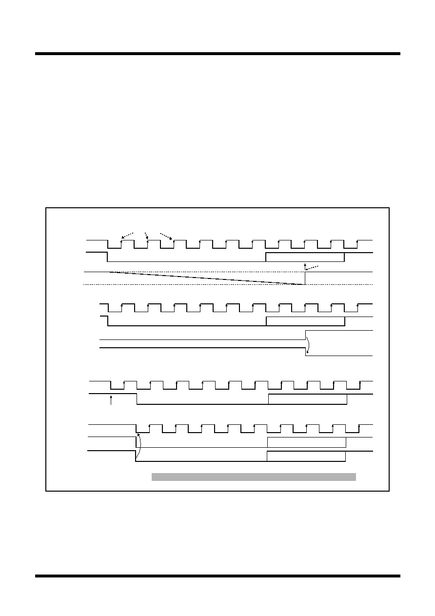
142
Tentative Specifications REV.A
Mitsubishi microcomputers
M16C / 62T Group
SINGLE-CHIP 16-BIT CMOS MICROCOMPUTER
S
pecifications in this manual are tentative and subject to change.
Under
development
UART2 Special Mode Register
1. Bus collision detect sampling clock select bit (Bit 4 of the UART2 special mode register)
0: Rising edges of the transfer clock
CLK
Timer A0
1: Timer A0 overflow
2. Auto clear function select bit of transmt enable bit (Bit 5 of the UART2 special mode register)
CLK
TxD/RxD
Bus collision
detect interrupt
request bit
Transmit
enable bit
3. Transmit start condition select bit (Bit 6 of the UART2 special mode register)
CLK
TxD
Enabling transmission
CLK
TxD
RxD
With "1: falling edge of RxD
2
" selected
0: In normal state
TxD/RxD
Note 1: In M30623(80-pin package), P7
2
/CLK
2
is not connected to external pin.
Figure 1.19.27. Some other functions added
Some other functions added are explained here. Figure 1.19.27 shows their workings.
Bit 4 of the UART2 special mode register is used as the bus collision detect sampling clock select bit. The
bus collision detect interrupt occurs when the RxD
2
level and TxD
2
level do not match, but the nonconfor-
mity is detected in synchronization with the rising edge of the transfer clock signal if the bit is set to "0". If
this bit is set to "1", the nonconformity is detected at the timing of the overflow of timer A0 rather than at
the rising edge of the transfer clock.
Bit 5 of the UART2 special mode register is used as the auto clear function select bit of transmit enable
bit. Setting this bit to "1" automatically resets the transmit enable bit to "0" when "1" is set in the bus
collision detect interrupt request bit (nonconformity).
Bit 6 of the UART2 special mode register is used as the transmit start condition select bit. Setting this bit
to "1" starts the TxD transmission in synchronization with the falling edge of the RxD terminal.
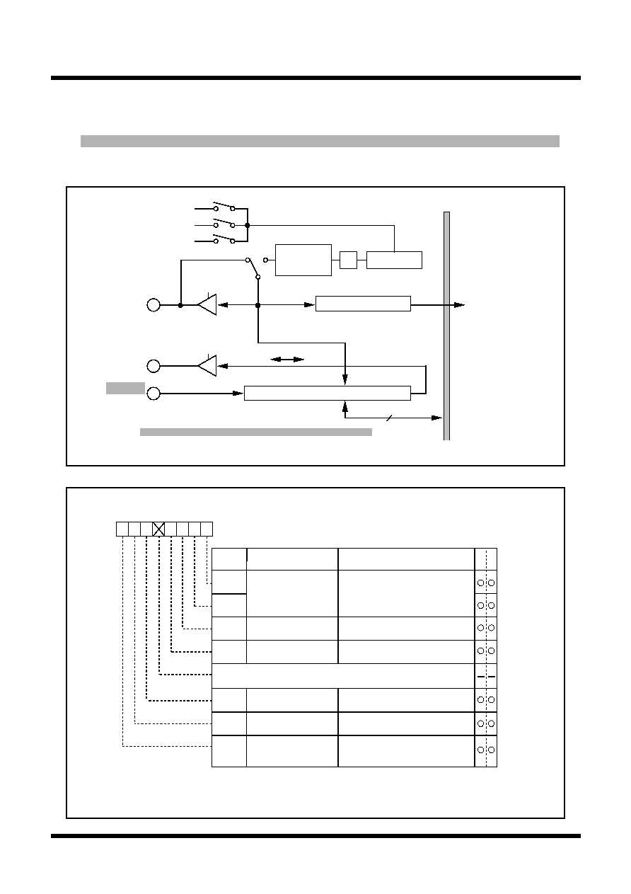
143
Tentative Specifications REV.A
Mitsubishi microcomputers
M16C / 62T Group
SINGLE-CHIP 16-BIT CMOS MICROCOMPUTER
S
pecifications in this manual are tentative and subject to change.
Under
development
UART2 Special Mode Register
S I/O3, 4
S I/O3 and S I/O4 are exclusive clock-synchronous serial I/Os.
In M30623(80-pin package), S
IN3
is not connected to external pin, so S I/O3 is exclusive transmission.
Figure 1.19.28 shows the S I/O3, 4 block diagram, and Figure 1.19.29 shows the S I/O3, 4 control register.
Table 1.19.10 shows the specifications of S I/O3, 4.
Figure 1.19.28. S I/O3, 4 block diagram
Figure 1.19.29. S I/O3, 4 control register
S I/O3, 4
S I/Oi transmission/reception register (8)
S I/O counter i (3)
Synchronous
circuit
f
1
f
8
f
32
Data bus
8
S I/Oi
interrupt request
SMi5 LSB MSB
SMi2
SMi3
SMi3
SMi6
SMi1
SMi0
P9
0/
CLK
3
(P9
5/
CLK
4
)
P9
2/
S
OUT3
(P9
6/
S
OUT4
)
P9
1/
S
IN3
(P9
7/
S
IN4
)
Transfer rate register (8)
SMi6
Note 1: In M30623(80-pin package), P9
1
/S
IN3
is not connected to external pin.
Note 2: i = 3, 4.
ni = A value set in the S I/O transfer rate register i (0363
16
, 0367
16
).
1/(ni+1)
1/2
S I/Oi control register (i = 3, 4) (Note 1)
Symbol
Address
When reset
SiC
0362
16
, 0366
16
40
16
b7
b6
b5
b4
b3
b2 b1
b0
W
R
Description
SMi5
SMi1
SMi0
SMi3
SMi6
SMi7
Internal synchronous
clock select bit
Transfer direction lect bit
S I/Oi port select bit
(Note 2)
S
OUT
i initial value
set bit
0 0 : Selecting f
1
0 1 : Selecting f
8
1 0 : Selecting f
32
1 1 : Not to be used
b1 b0
0 : External clock
1 : Internal clock
Effective when SMi3 = 0
0 : L output
1 : H output
0 : Input-output port
1 : S
OUT
i output, CLK function
Bit name
Bit
symbol
Synchronous clock
select bit (Note 2)
0 : LSB first
1 : MSB first
SMi2
S
OUT
i high impedance
control bit
0 : S
OUT
i output
1 : S
OUT
i high impedance
Note 1: Set "1" in bit 2 of the protection register (000A
16
) in advance to write to the
S I/Oi control register (i = 3, 4).
Note 2: When set "0" to SMi3 (i = 3, 4) and select input - output port, set "1" to SMi6
(i = 3, 4) and select internal clock, or input "H" to P9
0
and P9
5
.
Nothing is assigned.
In an attempt to write to this bit, write "0". The value, if read, turns out to be "0".
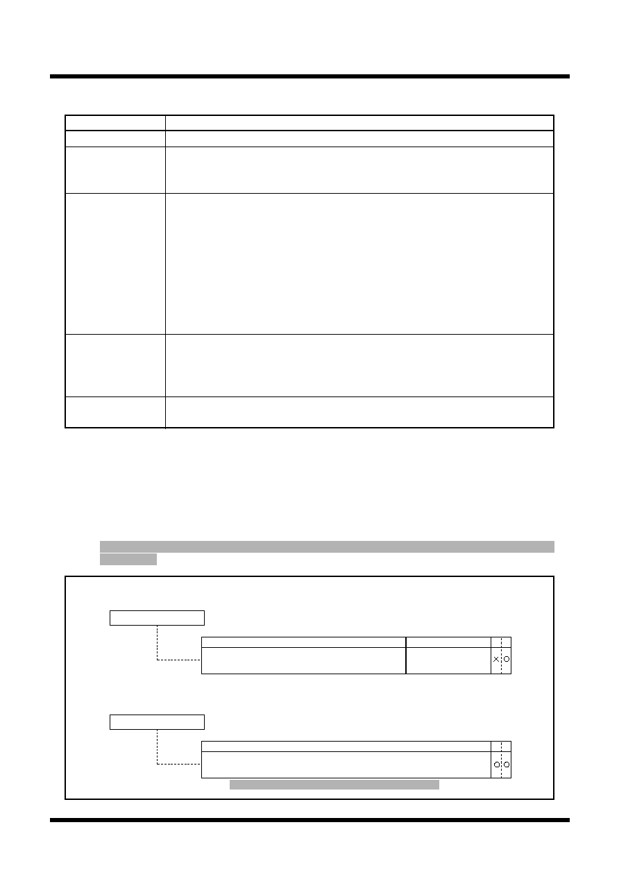
144
Tentative Specifications REV.A
Mitsubishi microcomputers
M16C / 62T Group
SINGLE-CHIP 16-BIT CMOS MICROCOMPUTER
S
pecifications in this manual are tentative and subject to change.
Under
development
UART2 Special Mode Register
Table 1.19.10. Specifications of S I/O3, 4
Note 1: n is a value from 00
16
through FF
16
set in the S I/Oi transfer rate register (i = 3, 4).
Note 2: With the external clock selected:
· To write to the S I/Oi transmission/reception register (0360
16
, 0364
16
), enter the "H" level to the CLKi
terminal. Also, to write to the bit 7 (S
OUT
i initial value set bit) of SI/Oi control register (0362
16
,
0366
16
), enter the "H" level to the CLKi terminal.
· The S I/Oi circuit keeps on with the shift operation as long as the synchronous clock is entered in it,
so stop the synchronous clock at the instant when it counts to eight. The internal clock, if selected,
automatically stops.
Note 3: If the internal clock is used for the synchronous clock, the transfer clock signal stops at the "H" state.
Note 4: In M30623(80-pin package), S I/O3 is exclusive transmission, because S
IN3
is not connected to
external pin.
Figure 1.19.30. SI/Oi related register
Item
Transfer data format
Transfer clock
Conditions for
transmission/
reception start
Interrupt request
generation timing
Select function
Specifications
· Transfer data length: 8 bits
· With the internal clock selected (bit 6 of 0362
16
, 0366
16
= "1"): f1/2(ni+1),
f8/2(ni+1), f32/2(ni+1) (Note 1)
· With the external clock selected (bit 6 of 0362
16
, 0366
16
= 0):Input from the CLKi terminal (Note 2)
· To start transmit/reception, the following requirements must be met:
- Select the synchronous clock (use bit 6 of 036216, 036616).
Select a frequency dividing ratio if the internal clock has been selected (use bits
0 and 1 of 0362
16
, 0366
16
).
- S
OUT
i initial value set bit (use bit 7 of 0362
16
, 0366
16
)= 1.
- S I/Oi port select bit (bit 3 of 0362
16
, 0366
16
) = 1.
- Select the transfer direction (use bit 5 of 0362
16
, 0366
16
)
· To use S I/Oi interrupts, the following requirements must be met:
- S I/Oi interrupt request bit (bit 3 of 0049
16
, 0048
16
) = 0.
· An interrupt occurs after counting eight transfer clock either in transmitting or
receiving data. (Note 3)
- In transmitting: At the time data transfer from the S I/Oi transmission/reception register finishes.
- In receiving: At the time data reception to the S I/Oi transmission/reception register finishes.
· LSB first or MSB first selection
Whether transmission/reception begins with bit 0 or bit 7 can be selected.
S I/O3, 4
SI/Oi bit rate generator
b7
b0
Symbol
Address
When reset
S3BRG
0363
16
Indeterminate
S4BRG
0367
16
Indeterminate
Indeterminate
Assuming that set value = n, BRGi divides the count
source by n + 1
00
16
to FF
16
Values that can be set
W
R
SI/Oi transmit/receive register
b7
b0
Symbol
Address
When reset
S3TRR
0360
16
Indeterminate
S4TRR
0364
16
Indeterminate
Indeterminate
Transmission/reception starts by writing data to this register.
After transmission/reception finishes, reception data is input. (Note 1)
W
R
Note 1: In M30623(80-package), S I/O3 is exclusive
transmission.
b7
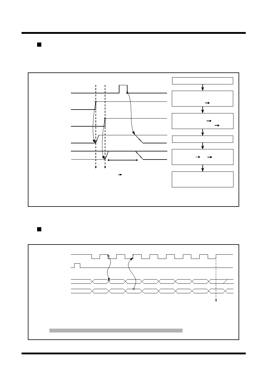
145
Tentative Specifications REV.A
Mitsubishi microcomputers
M16C / 62T Group
SINGLE-CHIP 16-BIT CMOS MICROCOMPUTER
S
pecifications in this manual are tentative and subject to change.
Under
development
UART2 Special Mode Register
Functions for setting an S
OUT
i initial value
In carrying out transmission, the output level of the SOUTi terminal as it is before transmitting 1-bit
data can be set either to "H" or to "L". Figure 1.19.31 shows the timing chart for setting an SOUTi initial
value and how to set it.
Figure 1.19.31. Timing chart for setting SOUTi's initial value and how to set it
S I/Oi operation timing
Figure 1.19.32 shows the S I/Oi operation timing
Figure 1.19.32. S I/Oi operation timing chart
S I/O3, 4
S I/Oi port select bit SMi3 = 0
SOUTi initial value select bit
SMi7 = 1
(S
OUT
i: Internal "H" level)
S I/Oi port select bit
SMi3 = 0 1
(Port select: Normal port S
OUT
i)
S
OUT
i terminal = "H" output
Signal written to the S I/Oi register
="L" "H" "L"
(Falling edge)
S
OUT
i terminal = Outputting
stored data in the S I/Oi transmission/
reception register
Signal written to the S I/Oi
transmission/reception
register
S
OUT
i (internal)
S
OUT
i's initial value
set bit (SMi7)
S
OUT
i terminal output
S I/Oi port select bit
(SMi3)
Setting the S
OUT
i
initial value to H
Port selection
(normal port S
OUT
i)
D0
(i = 3, 4)
Initial value = "H" (Note)
Port output
D0
(Example) With "H" selected for S
OUT
i:
Note: The set value is output only when the external clock has been selected. When
initializing S
OUT
i, input "H" level to CLKi pin.
If the internal clock has been selected or if S
OUT
high impedance has been set,
this output goes to the high-impedance state.
D
7
D
0
D
1
D
2
D
3
D
4
D
5
D
6
Transfer clock
(Note 1)
S I/Oi output S
OUT
i
S I/Oi input S
IN
i
Signal written to the
S I/Oi register
(Note 2)
Setting the S I/Oi interrupt request bit
Note 1: With the internal clock selected for the transfer clock, the frequency dividing ratio can be selected using
bits 0 and 1 of the S I/Oi control register. (No frequency division, 8-division frequency, 32-division frequency.)
Note 2: With the internal clock selected for the transfer clock, the S
OUT
i terminal becomes to the high-impedance
state after the transfer finishes.
Note 3: In M30623(80-pin package), the input pin S
IN3
of S
I/O3 is not connected to external pin.
(i= 3, 4)
(Note 3)
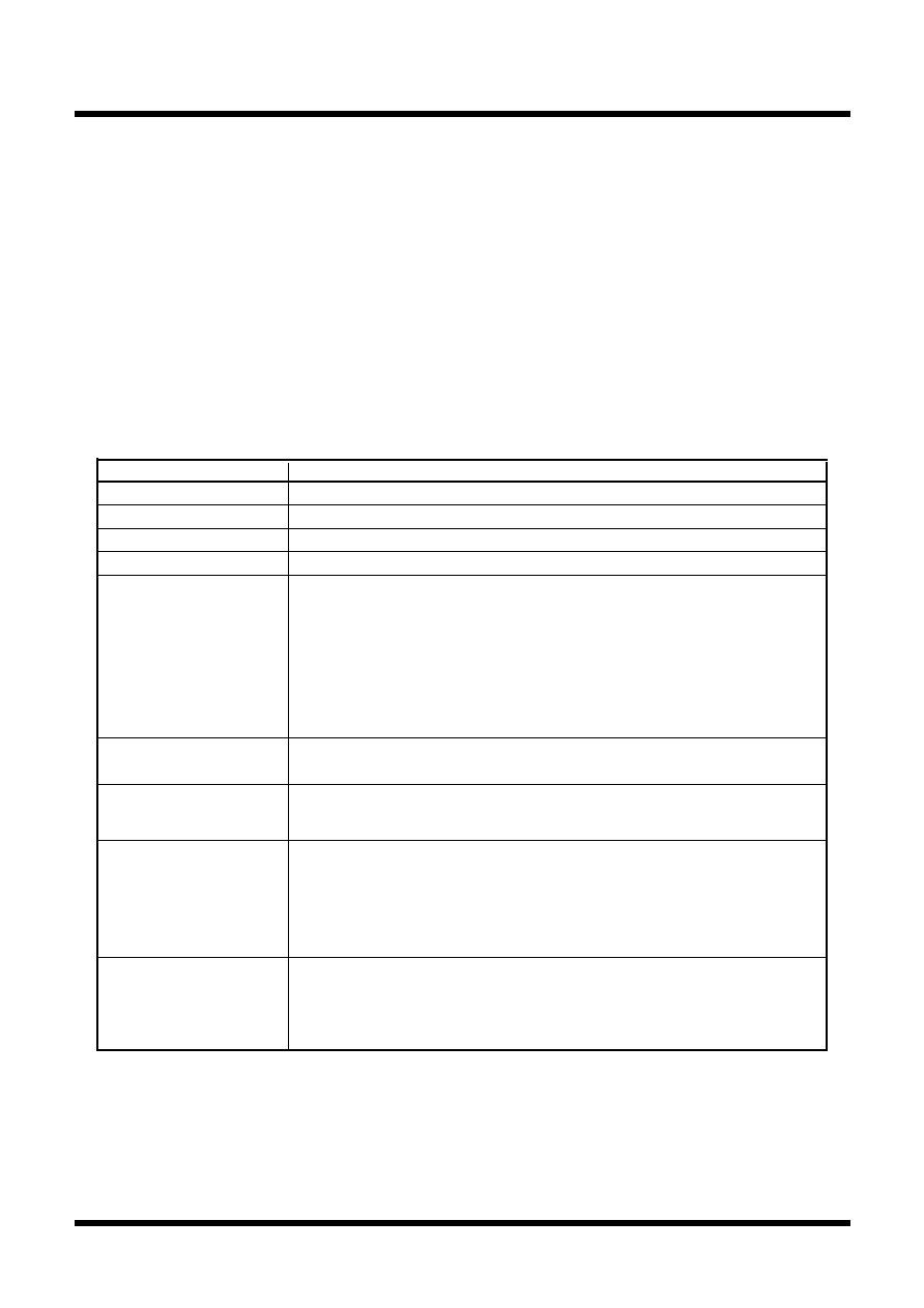
146
Tentative Specifications REV.A
Mitsubishi microcomputers
M16C / 62T Group
SINGLE-CHIP 16-BIT CMOS MICROCOMPUTER
S
pecifications in this manual are tentative and subject to change.
Under
development
A-D Converter
Item
Performance
Method of A-D conversion Successive approximation (capacitive coupling amplifier)
Analog input voltage (Note 1) 0V to AV
CC
(V
CC
)
Operating clock
AD
(Note 2) f
AD
/divide-by-2 of f
AD
/divide-by-4 of f
AD
, f
AD
=f(X
IN
) (V
CC
= 5V)
Resolution
8-bit or 10-bit (selectable)
Absolute precision
q
8-bit resolution
±
2LSB
q
10-bit resolution
±
3LSB
When the extended analog input pins ANEX0, ANEX1, AN
00
to AN
07,
and AN
20
to AN
27
are used as the external operation amp connection mode:
±
7LSB
Operating modes
One-shot mode, repeat mode, single sweep mode, repeat sweep mode 0,
and repeat sweep mode 1
Analog input pins
8 pins (AN
0
to AN
7
) + 2 pins (ANEX0 and ANEX1) + 16 pins (AN
00
to AN
07
,
AN
20
to AN
27
)
(Note 3)
A-D conversion start condition · Software trigger
A-D conversion starts when the A-D conversion start flag changes to "1"
· External trigger (can be retriggered)
A-D conversion starts when the A-D conversion start flag is "1" and the
___________
AD
TRG
/P9
7
input changes from "H" to "L"
Conversion speed per pin · Without sample and hold function
8-bit resolution: 49
AD
cycles, 10-bit resolution: 59
AD
cycles
· With sample and hold function
8-bit resolution: 28
AD
cycles, 10-bit resolution: 33
AD
cycles
A-D Converter
The A-D converter consists of one 10-bit successive approximation A-D converter circuit with a capacitive coupling
amplifier. Pins P10
0
to P10
7
, P9
5
, P9
6
, P0
0
to P0
7
, and P2
0
to P2
7
also function as the analog signal input pins. The
direction registers of these pins for A-D conversion must therefore be set to input. The Vref connect bit (bit 5 at
address 03D7
16
) can be used to isolate the resistance ladder of the A-D converter from the reference voltage input
pin (V
REF
) when the A-D converter is not used. Doing so stops any current flowing into the resistance ladder from
V
REF
, reducing the power dissipation. When using the A-D converter, start A-D conversion only after setting bit 5 of
03D7
16
to connect V
REF
.
The result of A-D conversion is stored in the A-D registers of the selected pins. When set to 10-bit precision, the low
8 bits are stored in the even addresses and the high 2 bits in the odd addresses. When set to 8-bit precision, the low
8 bits are stored in the even addresses.
Table 1.20.1 shows the performance of the A-D converter. Figure 1.20.1 shows the block diagram of the
A-D converter, and Figures 1.20.2 and 1.20.3 show the A-D converter-related registers.
Note 1: Does not depend on use of sample and hold function.
Note 2: Divide the frequency if f(X
IN
) exceeds 10MH
Z
, and make
AD
frequency equal to 10MH
Z
.
Without sample and hold function, set the
AD
frequency to 250kH
Z
min.
With the sample and hold function, set the
AD
frequency to 1MH
Z
min.
Note 3: The pins are not used as the analog input pins can be used as normal I/O ports, or I/O pins of
each peripheral function.
Table 1.20.1. Performance of A-D converter
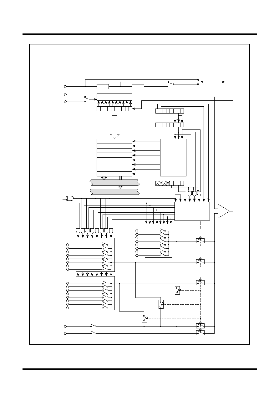
147
Tentative Specifications REV.A
Mitsubishi microcomputers
M16C / 62T Group
SINGLE-CHIP 16-BIT CMOS MICROCOMPUTER
S
pecifications in this manual are tentative and subject to change.
Under
development
A-D Converter
Figure 1.20.1. Block diagram of A-D converter
P2
0
/AN
20
P2
1
/AN
21
P2
2
/AN
22
P2
3
/AN
23
P2
4
/AN
24
P2
5
/AN
25
P2
6
/AN
26
P2
7
/AN
27
ANEX
0
ANEX
1
OPA0 = 1
OPA1 = 1
PM01,PM00 = 00
ADGSEL1,ADGSEL0 = 11
OPA1,OPA0 = 11
PM01,PM00 = 00
ADGSEL1,ADGSEL0 = 10
OPA1,OPA0 = 11
ADGSEL1,ADGSEL0 = 00
OPA1,OPA0 = 11
= 000
= 001
= 010
= 011
= 100
= 101
= 110
= 111
P10
0
/AN
0
P10
1
/AN
1
P10
2
/AN
2
P10
3
/AN
3
P10
4
/AN
4
P10
5
/AN
5
P10
6
/AN
6
P10
7
/AN
7
= 00000
= 00001
= 00010
= 00011
= 00100
= 00101
= 00110
= 00111
PM01,PM00,CH2,CH1,CH0
P0
0
/AN
00
P0
1
/AN
01
P0
2
/AN
02
P0
3
/AN
03
P0
4
/AN
04
P0
5
/AN
05
P0
6
/AN
06
P0
7
/AN
07
= 00000
= 00001
= 00010
= 00011
= 00100
= 00101
= 00110
= 00111
PM01,PM00,CH2,CH1,CH0
V
ref
V
IN
CH2,CH1,CH0
PM00
PM01
Decoder
for channel selection
A-D register 0 (16)
A-D register 1 (16)
A-D register 2 (16)
A-D register 3 (16)
A-D register 4 (16)
A-D register 5 (16)
A-D register 6 (16)
A-D register 7 (16)
(03C1
16
, 03C0
16
)
(03C3
16
, 03C2
16
)
(03C5
16
, 03C4
16
)
(03C7
16
, 03C6
16
)
(03C9
16
, 03C8
16
)
(03CB
16
, 03CA
16
)
(03CD
16
, 03CC
16
)
(03CF
16
, 03CE
16
)
A-D control register 0
(address 03D6
16
)
A-D control register 1
(address 03D7
16
)
Successive conversion register
Resistor ladder
Data bus low-order
V
REF
AV
SS
VCUT = 0
VCUT = 1
f
AD
AD
1/2
1/2
A-D conversion rate selection
CKS0 = 1
CKS0 = 0
CKS1 = 1
CKS1 = 0
Data bus high-order
A-D control register 2
(address 03D4
16
)
Decoder
for A-D register
OPA1 = 1
Port P10 group
Port P0 group
Port P2 group
PM01,PM00 = 00
ADGSEL1,ADGSEL0 = 10
OPA1,OPA0 = 00
PM01,PM00 = 00
ADGSEL1,ADGSEL0 = 11
OPA1,OPA0 = 00
ADGSEL1,ADGSEL0 = 00
OPA1,OPA0 = 00
OPA1,OPA0
= 01
Addresses
Comparator
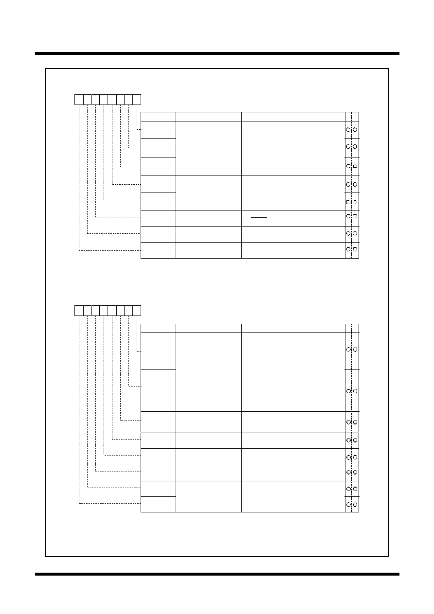
148
Tentative Specifications REV.A
Mitsubishi microcomputers
M16C / 62T Group
SINGLE-CHIP 16-BIT CMOS MICROCOMPUTER
S
pecifications in this manual are tentative and subject to change.
Under
development
A-D Converter
Figure 1.20.2. A-D converter-related registers (1)
A
-
D
c
o
n
t
r
o
l
r
e
g
i
s
t
e
r
0
(
N
o
t
e
1
)
S
y
m
b
o
l
A
d
d
r
e
s
s
W
h
e
n
r
e
s
e
t
A
D
C
O
N
0
0
3
D
6
1
6
0
0
0
0
0
X
X
X
2
b
7
b
6
b
5
b
4
b
3
b
2
b
1
b
0
A
n
a
l
o
g
i
n
p
u
t
p
i
n
s
e
l
e
c
t
b
i
t
0
0
0
:
A
N
0
i
s
s
e
l
e
c
t
e
d
0
0
1
:
A
N
1
i
s
s
e
l
e
c
t
e
d
0
1
0
:
A
N
2
i
s
s
e
l
e
c
t
e
d
0
1
1
:
A
N
3
i
s
s
e
l
e
c
t
e
d
1
0
0
:
A
N
4
i
s
s
e
l
e
c
t
e
d
1
0
1
:
A
N
5
i
s
s
e
l
e
c
t
e
d
1
1
0
:
A
N
6
i
s
s
e
l
e
c
t
e
d
(
N
o
t
e
2
)
1
1
1
:
A
N
7
i
s
s
e
l
e
c
t
e
d
(
N
o
t
e
3
)
C
H
0
B
i
t
s
y
m
b
o
l
B
i
t
n
a
m
e
F
u
n
c
t
i
o
n
C
H
1
C
H
2
A
-
D
o
p
e
r
a
t
i
o
n
m
o
d
e
s
e
l
e
c
t
b
i
t
0
0
0
:
O
n
e
-
s
h
o
t
m
o
d
e
0
1
:
R
e
p
e
a
t
m
o
d
e
1
0
:
S
i
n
g
l
e
s
w
e
e
p
m
o
d
e
1
1
:
R
e
p
e
a
t
s
w
e
e
p
m
o
d
e
0
R
e
p
e
a
t
s
w
e
e
p
m
o
d
e
1
(
N
o
t
e
3
)
M
D
0
M
D
1
T
r
i
g
g
e
r
s
e
l
e
c
t
b
i
t
0
:
S
o
f
t
w
a
r
e
t
r
i
g
g
e
r
1
:
A
D
T
R
G
t
r
i
g
g
e
r
T
R
G
A
D
S
T
A
-
D
c
o
n
v
e
r
s
i
o
n
s
t
a
r
t
f
l
a
g
0
:
A
-
D
c
o
n
v
e
r
s
i
o
n
d
i
s
a
b
l
e
d
1
:
A
-
D
c
o
n
v
e
r
s
i
o
n
s
t
a
r
t
e
d
F
r
e
q
u
e
n
c
y
s
e
l
e
c
t
b
i
t
0
0
:
f
A
D
/
4
i
s
s
e
l
e
c
t
e
d
1
:
f
A
D
/
2
i
s
s
e
l
e
c
t
e
d
C
K
S
0
W
R
A
-
D
c
o
n
t
r
o
l
r
e
g
i
s
t
e
r
1
(
N
o
t
e
1
)
S
y
m
b
o
l
A
d
d
r
e
s
s
W
h
e
n
r
e
s
e
t
A
D
C
O
N
1
0
3
D
7
1
6
0
0
1
6
B
i
t
n
a
m
e
F
u
n
c
t
i
o
n
B
i
t
s
y
m
b
o
l
b
7
b
6
b
5
b
4
b
3
b
2
b
1
b
0
A
-
D
s
w
e
e
p
p
i
n
s
e
l
e
c
t
b
i
t
S
C
A
N
0
S
C
A
N
1
M
D
2
B
I
T
S
8
/
1
0
-
b
i
t
m
o
d
e
s
e
l
e
c
t
b
i
t
0
:
8
-
b
i
t
m
o
d
e
1
:
1
0
-
b
i
t
m
o
d
e
V
C
U
T
O
P
A
0
V
r
e
f
c
o
n
n
e
c
t
b
i
t
O
P
A
1
A
-
D
o
p
e
r
a
t
i
o
n
m
o
d
e
s
e
l
e
c
t
b
i
t
1
0
:
A
n
y
m
o
d
e
o
t
h
e
r
t
h
a
n
r
e
p
e
a
t
s
w
e
e
p
m
o
d
e
1
1
:
R
e
p
e
a
t
s
w
e
e
p
m
o
d
e
1
0
:
V
r
e
f
n
o
t
c
o
n
n
e
c
t
e
d
1
:
V
r
e
f
c
o
n
n
e
c
t
e
d
E
x
t
e
r
n
a
l
o
p
-
a
m
p
c
o
n
n
e
c
t
i
o
n
m
o
d
e
b
i
t
W
R
b
2
b
1
b
0
b
4
b
3
W
h
e
n
s
i
n
g
l
e
s
w
e
e
p
a
n
d
r
e
p
e
a
t
s
w
e
e
p
m
o
d
e
0
a
r
e
s
e
l
e
c
t
e
d
0
0
:
A
N
0
,
A
N
1
(
2
p
i
n
s
)
0
1
:
A
N
0
t
o
A
N
3
(
4
p
i
n
s
)
1
0
:
A
N
0
t
o
A
N
5
(
6
p
i
n
s
)
1
1
:
A
N
0
t
o
A
N
7
(
8
p
i
n
s
)
b
1
b
0
W
h
e
n
r
e
p
e
a
t
s
w
e
e
p
m
o
d
e
1
i
s
s
e
l
e
c
t
e
d
0
0
:
A
N
0
(
1
p
i
n
)
0
1
:
A
N
0
,
A
N
1
(
2
p
i
n
s
)
1
0
:
A
N
0
t
o
A
N
2
(
3
p
i
n
s
)
1
1
:
A
N
0
t
o
A
N
3
(
4
p
i
n
s
)
(
N
o
t
e
3
)
b
1
b
0
0
0
:
A
N
E
X
0
a
n
d
A
N
E
X
1
a
r
e
n
o
t
u
s
e
d
0
1
:
A
N
E
X
0
i
n
p
u
t
i
s
A
-
D
c
o
n
v
e
r
t
e
d
1
0
:
A
N
E
X
1
i
n
p
u
t
i
s
A
-
D
c
o
n
v
e
r
t
e
d
1
1
:
E
x
t
e
r
n
a
l
o
p
-
a
m
p
c
o
n
n
e
c
t
i
o
n
m
o
d
e
b
7
b
6
N
o
t
e
1
:
I
f
t
h
e
A
-
D
c
o
n
t
r
o
l
r
e
g
i
s
t
e
r
i
s
r
e
w
r
i
t
t
e
n
d
u
r
i
n
g
A
-
D
c
o
n
v
e
r
s
i
o
n
,
t
h
e
c
o
n
v
e
r
s
i
o
n
r
e
s
u
l
t
i
s
i
n
d
e
t
e
r
m
i
n
a
t
e
.
N
o
t
e
2
:
A
N
0
0
t
o
A
N
0
7
,
a
n
d
A
N
2
0
t
o
A
N
2
7
c
a
n
b
e
u
s
e
d
t
h
e
s
a
m
e
a
s
A
N
0
t
o
A
N
7
.
N
o
t
e
3
:
W
h
e
n
c
h
a
n
g
i
n
g
A
-
D
o
p
e
r
a
t
i
o
n
m
o
d
e
,
s
e
t
a
n
a
l
o
g
i
n
p
u
t
p
i
n
a
g
a
i
n
.
F
r
e
q
u
e
n
c
y
s
e
l
e
c
t
b
i
t
1
0
:
f
A
D
/
2
o
r
f
A
D
/
4
i
s
s
e
l
e
c
t
e
d
1
:
f
A
D
i
s
s
e
l
e
c
t
e
d
C
K
S
1
N
o
t
e
1
:
I
f
t
h
e
A
-
D
c
o
n
t
r
o
l
r
e
g
i
s
t
e
r
i
s
r
e
w
r
i
t
t
e
n
d
u
r
i
n
g
A
-
D
c
o
n
v
e
r
s
i
o
n
,
t
h
e
c
o
n
v
e
r
s
i
o
n
r
e
s
u
l
t
i
s
i
n
d
e
t
e
r
m
i
n
a
t
e
.
N
o
t
e
2
:
D
i
v
i
d
e
t
h
e
f
r
e
q
u
e
n
c
y
i
f
f
(
X
I
N
)
e
x
c
e
e
d
s
1
0
M
H
z
,
a
n
d
m
a
k
e
A
D
f
r
e
q
u
e
n
c
y
e
q
u
a
l
t
o
1
0
M
H
z
.
N
o
t
e
3
:
A
N
0
0
t
o
A
N
0
7
,
a
n
d
A
N
2
0
t
o
A
N
2
7
c
a
n
b
e
u
s
e
d
t
h
e
s
a
m
e
a
s
A
N
0
t
o
A
N
7
.
(
N
o
t
e
2
)
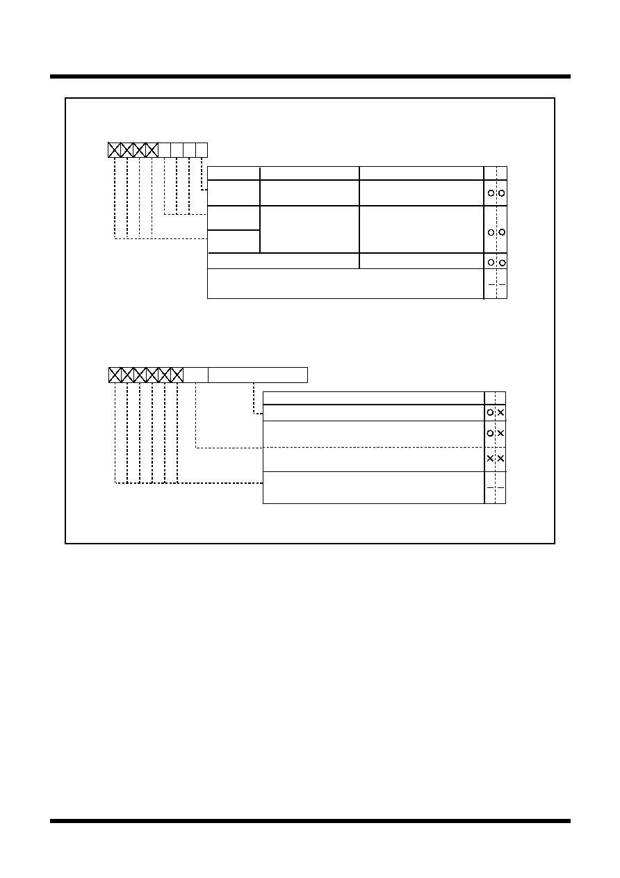
149
Tentative Specifications REV.A
Mitsubishi microcomputers
M16C / 62T Group
SINGLE-CHIP 16-BIT CMOS MICROCOMPUTER
S
pecifications in this manual are tentative and subject to change.
Under
development
A-D Converter
Figure 1.20.3. A-D converter-related registers (2)
A-D control register 2 (Note)
Symbol
Address
When reset
ADCON2
03D4
16
00
16
b7
b6
b5
b4
b3
b2
b1
b0
A-D conversion method
select bit
0 : Without sample and hold
1 : With sample and hold
Bit symbol
Bit name
Function
R W
Note: If the A-D control register is rewritten during A-D conversion, the conversion
result is indeterminate.
Nothing is assigned.
In an attempt to write to these bits, write "0". The value, if read, turns out to
be "0".
A-D register i
Symbol
Address
When reset
ADi(i=0 to 7)
03C0
16
to 03CF
16
Indeterminate
Eight low-order bits of A-D conversion result
Function
R W
(b15)
b7
b7
b0
b0
(b8)
· During 10-bit mode
Two high-order bits of A-D conversion result
Nothing is assigned.
In an attempt to write to these bits, write "0". The value, if
read, turns out to be "0".
· During 8-bit mode
When read, the content is indeterminate
SMP
0
ADGSEL0
ADGSEL1
Analog input group
select bit
00 : Port10 group is selected
01 : Not use
10 : Port0 group is selected
11 : Port1 group is selected
b2 b1
Reserved bit
Always set to "0"
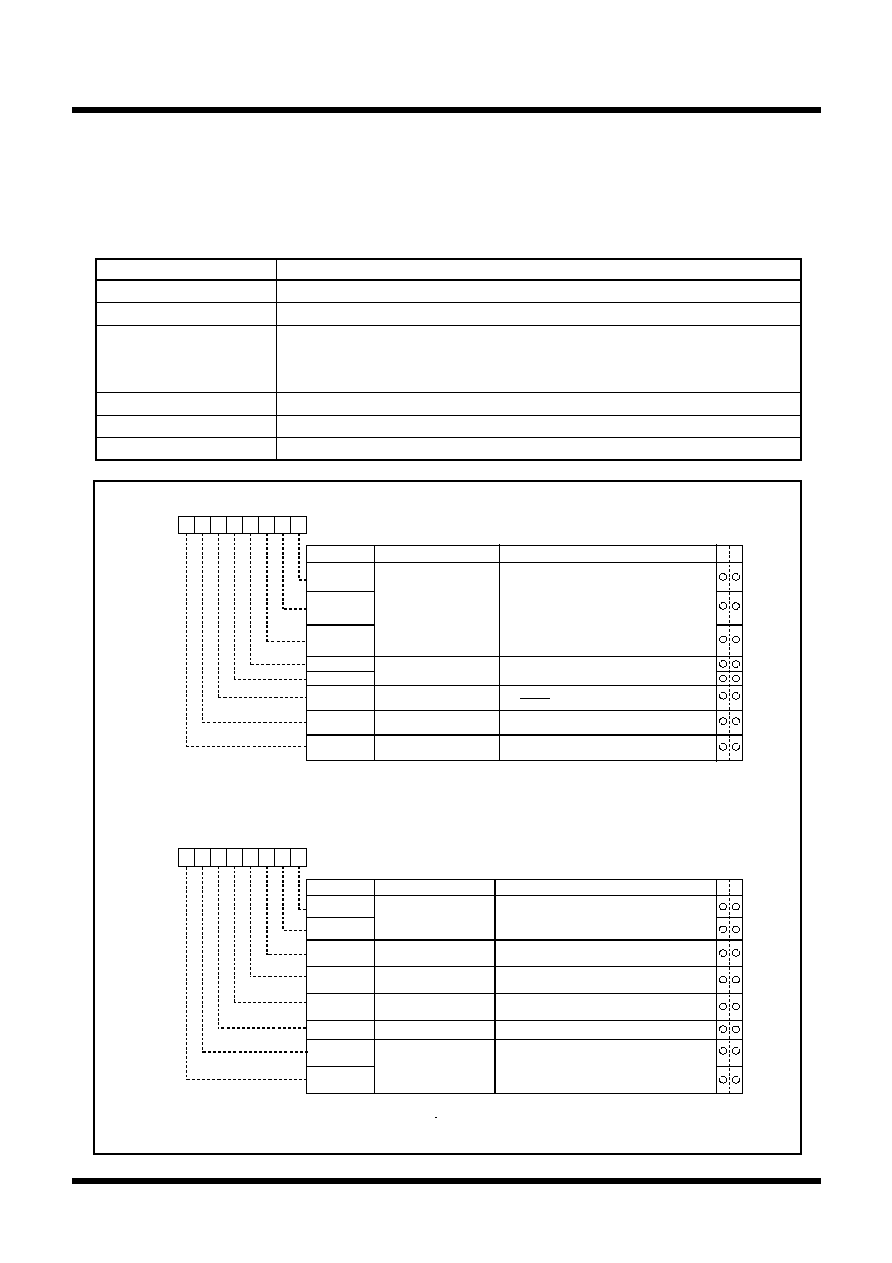
150
Tentative Specifications REV.A
Mitsubishi microcomputers
M16C / 62T Group
SINGLE-CHIP 16-BIT CMOS MICROCOMPUTER
S
pecifications in this manual are tentative and subject to change.
Under
development
A-D Converter
(1) One-shot mode
In one-shot mode, the pin selected using the analog input pin select bit is used for one-shot A-D conver-
sion. Table 1.20.2 shows the specifications of one-shot mode. Figure 1.20.4 shows the A-D control regis-
ter in one-shot mode.
Table 1.20.2. One-shot mode specifications
Figure 1.20.4. A-D conversion register in one-shot mode
A-D control register 0 (Note 1)
Symbol
Address
When reset
ADCON0
03D6
16
00000XXX
2
b7
b6
b5
b4
b3
b2
b1
b0
Analog input pin
select bit
CH0
Bit symbol
Bit name
Function
CH1
CH2
A-D operation mode
select bit 0
MD0
MD1
Trigger select bit
0 : Software trigger
1 : AD
TRG
trigger
TRG
ADST
A-D conversion start flag
0 : A-D conversion disabled
1 : A-D conversion started
Frequency select bit 0
0 : f
AD
/4 is selected
1 : f
AD
/2 is selected
CKS0
W
R
A-D control register 1 (Note 1)
Symbol
Address
When reset
ADCON1
03D7
16
00
16
Bit name
Function
Bit symbol
b7
b6
b5
b4
b3
b2
b1
b0
A-D sweep pin select bit
SCAN0
SCAN1
MD2
BITS
8/10-bit mode select bit
0 : 8-bit mode
1 : 10-bit mode
VCUT
OPA0
Vref connect bit
OPA1
A-D operation mode
select bit 1
1 : Vref connected
External op-amp
connection mode bit
W
R
0
0
Invalid in one-shot mode
0
0 0 0 : AN
0
is selected
0 0 1 : AN
1
is selected
0 1 0 : AN
2
is selected
0 1 1 : AN
3
is selected
1 0 0 : AN
4
is selected
1 0 1 : AN
5
is selected
1 1 0 : AN
6
is selected
(Note 2)
1 1 1 : AN
7
is selected
(Note 3)
b2 b1 b0
0 0 : One-shot mode
(Note 3)
b4 b3
0 0 : ANEX0 and ANEX1 are not used
0 1 : ANEX0 input is A-D converted
1 0 : ANEX1 input is A-D converted
1 1 : External op-amp connection mode
b7 b6
1
Note 1: If the A-D control register is rewritten during A-D conversion, the conversion
result is indeterminate.
Note 2: AN
00
to AN
07
, and AN
20
to AN
27
can be used the same as AN
0
to AN
7
.
Note 3: When changing A-D operation mode, set analog input pin again.
Frequency select bit 1
0 : f
AD
/2 or f
AD
/4 is selected
1 : f
AD
is selected
CKS1
0 : Any mode other than repeat sweep mode 1
Note 1: If the A-D control register is rewritten during A-D conversion, the conversion
result is indeterminate.
Note 2: Divide the frequency if f(X
IN
) exceeds 10MHz, and make
AD
frequency
equal to 10MHz.
(Note 2)
Item
Specification
Function
The pin selected by the analog input pin select bit is used for one A-D conversion
Start condition
Writing "1" to A-D conversion start flag
Stop condition
· End of A-D conversion (A-D conversion start flag changes to "0", except
when external trigger is selected)
· Writing "0" to A-D conversion start flag
Interrupt request generation timing
End of A-D conversion
Input pin
One of AN
0
to AN
7
, as selected
(Note 1)
Reading of result of A-D converter
Read A-D register corresponding to selected pin
Note 1: AN
00
to AN
07
, and AN
20
to AN
27
can be used the same as AN
0
to AN
7
.
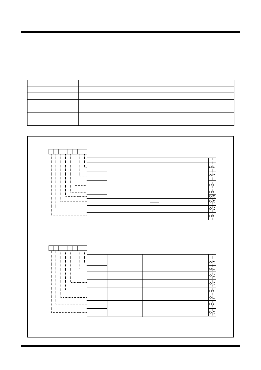
151
Tentative Specifications REV.A
Mitsubishi microcomputers
M16C / 62T Group
SINGLE-CHIP 16-BIT CMOS MICROCOMPUTER
S
pecifications in this manual are tentative and subject to change.
Under
development
A-D Converter
(2) Repeat mode
In repeat mode, the pin selected using the analog input pin select bit is used for repeated A-D conversion.
Table 1.20.3 shows the specifications of repeat mode. Figure 1.20.5 shows the A-D control register in
repeat mode.
A-D control register 0 (Note 1)
Symbol
Address
When reset
ADCON0
03D6
16
00000XXX
2
b7
b6
b5
b4
b3
b2
b1
b0
Analog input pin
select bit
CH0
Bit symbol
Bit name
Function
CH1
CH2
A-D operation mode
select bit 0
MD0
MD1
Trigger select bit
0 : Software trigger
1 : AD
TRG
trigger
TRG
ADST
A-D conversion start flag
0 : A-D conversion disabled
1 : A-D conversion started
Frequency select bit 0
0 : f
AD
/4 is selected
1 : f
AD
/2 is selected
CKS0
W
R
A-D control register 1 (Note 1)
Symbol
Address
When reset
ADCON1
03D7
16
00
16
Bit name
Function
Bit symbol
b7
b6
b5
b4
b3
b2
b1
b0
A-D sweep pin select bit
SCAN0
SCAN1
MD2
BITS
8/10-bit mode select bit
0 : 8-bit mode
1 : 10-bit mode
VCUT
OPA0
Vref connect bit
OPA1
A-D operation mode
select bit 1
1 : Vref connected
External op-amp
connection mode bit
W
R
0
1
Invalid in repeat mode
0
0 0 0 : AN
0
is selected
0 0 1 : AN
1
is selected
0 1 0 : AN
2
is selected
0 1 1 : AN
3
is selected
1 0 0 : AN
4
is selected
1 0 1 : AN
5
is selected
1 1 0 : AN
6
is selected
(Note 2)
1 1 1 : AN
7
is selected
(Note 3)
b2 b1 b0
0 1 : Repeat mode
(Note 3)
b4 b3
0 0 : ANEX0 and ANEX1 are not used
0 1 : ANEX0 input is A-D converted
1 0 : ANEX1 input is A-D converted
1 1 : External op-amp connection mode
b7 b6
1
Note 1: If the A-D control register is rewritten during A-D conversion, the conversion
result is indeterminate.
Note 2: AN
00
to AN
07
, and AN
20
to AN
27
can be used the same as AN
0
to AN
7
.
Note 3: When changing A-D operation mode, set analog input pin again.
Frequency select bit 1
0 : f
AD
/2 or f
AD
/4 is selected
1 : f
AD
is selected
CKS1
0 : Any mode other than repeat sweep mode 1
Note 1: If the A-D control register is rewritten during A-D conversion, the conversion
result is indeterminate.
Note 2: Divide the frequency if f(X
IN
) exceeds 10MHz, and make
AD
frequency
equal to 10MHz.
(Note 2)
Figure 1.20.5. A-D conversion register in repeat mode
Item
Specification
Function
The pin selected by the analog input pin select bit is used for repeated A-D conversion
Star condition
Writing "1" to A-D conversion start flag
Stop condition
Writing "0" to A-D conversion start flag
Interrupt request generation timing
None generated
Input pin
One of AN
0
to AN
7
, as selected
(Note 1)
Reading of result of A-D converter
Read A-D register corresponding to selected pin
Table 1.20.3. Repeat mode specifications
Note 1: AN
00
to AN
07
, and AN
20
to AN
27
can be used the same as AN
0
to AN
7
.
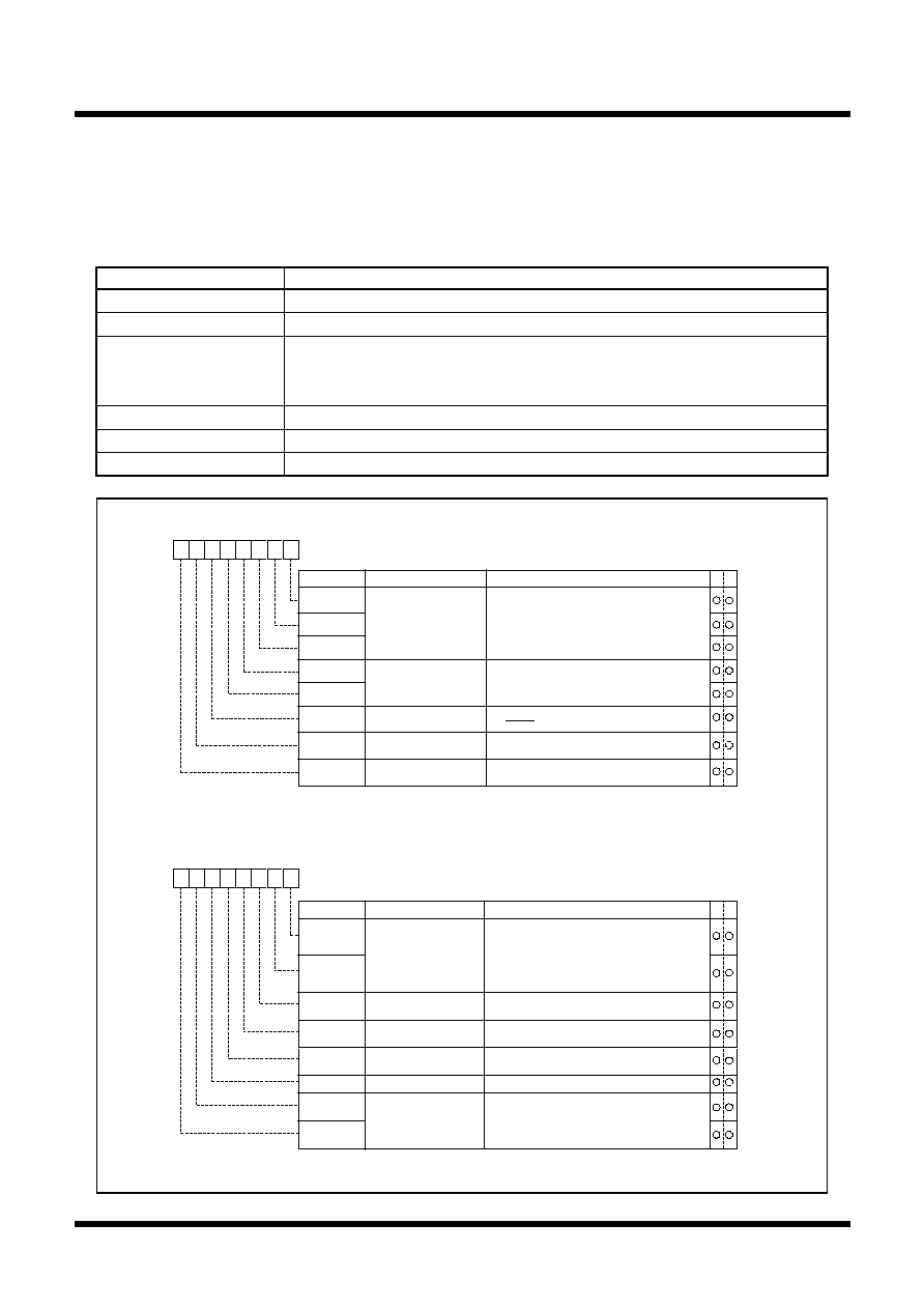
152
Tentative Specifications REV.A
Mitsubishi microcomputers
M16C / 62T Group
SINGLE-CHIP 16-BIT CMOS MICROCOMPUTER
S
pecifications in this manual are tentative and subject to change.
Under
development
A-D Converter
(3) Single sweep mode
In single sweep mode, the pins selected using the A-D sweep pin select bit are used for one-by-one A-D
conversion. Table 1.20.4 shows the specifications of single sweep mode. Figure 1.20.6 shows the A-D
control register in single sweep mode.
Table 1.20.4. Single sweep mode specifications
Figure 1.20.6. A-D conversion register in single sweep mode
A
-
D
c
o
n
t
r
o
l
r
e
g
i
s
t
e
r
0 (
N
o
t
e
1
)
S
y
m
b
o
l
A
d
d
r
e
s
s
W
h
e
n
r
e
s
e
t
A
D
C
O
N
0
0
3
D
6
1
6
0
0
0
0
0
X
X
X
2
b
7
b
6
b
5
b
4
b
3
b
2
b
1
b
0
A
n
a
l
o
g
i
n
p
u
t
p
i
n
s
e
l
e
c
t
b
i
t
C
H
0
B
i
t
s
y
m
b
o
l
B
i
t
n
a
m
e
F
u
n
c
t
i
o
n
C
H
1
C
H
2
A
-
D
o
p
e
r
a
t
i
o
n
m
o
d
e
s
e
l
e
c
t
b
i
t
0
1
0
:
S
i
n
g
l
e
s
w
e
e
p
m
o
d
e
M
D
0
M
D
1
T
r
i
g
g
e
r
s
e
l
e
c
t
b
i
t
0
:
S
o
f
t
w
a
r
e
t
r
i
g
g
e
r
1
:
A
D
T
R
G
t
r
i
g
g
e
r
T
R
G
A
D
S
T
A
-
D
c
o
n
v
e
r
s
i
o
n
s
t
a
r
t
f
l
a
g
0
:
A
-
D
c
o
n
v
e
r
s
i
o
n
d
i
s
a
b
l
e
d
1
:
A
-
D
c
o
n
v
e
r
s
i
o
n
s
t
a
r
t
e
d
F
r
e
q
u
e
n
c
y
s
e
l
e
c
t
b
i
t
0
0
:
f
A
D
/
4
i
s
s
e
l
e
c
t
e
d
1
:
f
A
D
/
2
i
s
s
e
l
e
c
t
e
d
C
K
S
0
W
R
A
-
D
c
o
n
t
r
o
l
r
e
g
i
s
t
e
r
1
(
N
o
t
e
1
)
S
y
m
b
o
l
A
d
d
r
e
s
s
W
h
e
n
r
e
s
e
t
A
D
C
O
N
1
0
3
D
7
1
6
0
0
1
6
B
i
t
n
a
m
e
F
u
n
c
t
i
o
n
B
i
t
s
y
m
b
o
l
b
7
b
6
b
5
b
4
b
3
b
2
b
1
b
0
A
-
D
s
w
e
e
p
p
i
n
s
e
l
e
c
t
b
i
t
S
C
A
N
0
S
C
A
N
1
M
D
2
B
I
T
S
8
/
1
0
-
b
i
t
m
o
d
e
s
e
l
e
c
t
b
i
t
0
:
8
-
b
i
t
m
o
d
e
1
:
1
0
-
b
i
t
m
o
d
e
V
C
U
T
O
P
A
0
V
r
e
f
c
o
n
n
e
c
t
b
i
t
0
:
A
n
y
m
o
d
e
o
t
h
e
r
t
h
a
n
r
e
p
e
a
t
s
w
e
e
p
m
o
d
e
1
O
P
A
1
A
-
D
o
p
e
r
a
t
i
o
n
m
o
d
e
s
e
l
e
c
t
b
i
t
1
1
:
V
r
e
f
c
o
n
n
e
c
t
e
d
E
x
t
e
r
n
a
l
o
p
-
a
m
p
c
o
n
n
e
c
t
i
o
n
m
o
d
e
b
i
t
(
N
o
t
e
4
)
W
R
1 0
I
n
v
a
l
i
d
i
n
s
i
n
g
l
e
s
w
e
e
p
m
o
d
e
0
b
4
b
3
W
h
e
n
s
i
n
g
l
e
s
w
e
e
p
a
n
d
r
e
p
e
a
t
s
w
e
e
p
m
o
d
e
0
a
r
e
s
e
l
e
c
t
e
d
0
0
:
A
N
0
,
A
N
1
(
2
p
i
n
s
)
0
1
:
A
N
0
t
o
A
N
3
(
4
p
i
n
s
)
1
0
:
A
N
0
t
o
A
N
5
(
6
p
i
n
s
)
1
1
:
A
N
0
t
o
A
N
7
(
8
p
i
n
s
)
b
1
b
0
0
0
:
A
N
E
X
0
a
n
d
A
N
E
X
1
a
r
e
n
o
t
u
s
e
d
0
1
:
A
N
E
X
0
i
n
p
u
t
i
s
A
-
D
c
o
n
v
e
r
t
e
d
1
0
:
A
N
E
X
1
i
n
p
u
t
i
s
A
-
D
c
o
n
v
e
r
t
e
d
1
1
:
E
x
t
e
r
n
a
l
o
p
-
a
m
p
c
o
n
n
e
c
t
i
o
n
m
o
d
e
b
7
b
6
1
N
o
t
e
1
:
I
f
t
h
e
A
-
D
c
o
n
t
r
o
l
r
e
g
i
s
t
e
r
i
s
r
e
w
r
i
t
t
e
n
d
u
r
i
n
g
A
-
D
c
o
n
v
e
r
s
i
o
n
,
t
h
e
c
o
n
v
e
r
s
i
o
n
r
e
s
u
l
t
i
s
i
n
d
e
t
e
r
m
i
n
a
t
e
.
F
r
e
q
u
e
n
c
y
s
e
l
e
c
t
b
i
t
1
0
:
f
A
D
/
2
o
r
f
A
D
/
4
i
s
s
e
l
e
c
t
e
d
1
:
f
A
D
i
s
s
e
l
e
c
t
e
d
C
K
S
1
(
N
o
t
e
3
)
(
N
o
t
e
2
)
N
o
t
e
1
:
I
f
t
h
e
A
-
D
c
o
n
t
r
o
l
r
e
g
i
s
t
e
r
i
s
r
e
w
r
i
t
t
e
n
d
u
r
i
n
g
A
-
D
c
o
n
v
e
r
s
i
o
n
,
t
h
e
c
o
n
v
e
r
s
i
o
n
r
e
s
u
l
t
i
s
i
n
d
e
t
e
r
m
i
n
a
t
e
.
N
o
t
e
2
:
D
i
v
i
d
e
t
h
e
f
r
e
q
u
e
n
c
y
i
f
f
(
X
I
N
)
e
x
c
e
e
d
s
1
0
M
H
z
,
a
n
d
m
a
k
e
A
D
f
r
e
q
u
e
n
c
y
e
q
u
a
l
t
1
0
M
H
Item
Specification
Function
The pins selected by the A-D sweep pin select bit are used for one-by-one A-D conversion
Start condition
Writing "1" to A-D converter start flag
Stop condition
· End of A-D conversion (A-D conversion start flag changes to "0", except
when external trigger is selected)
· Writing "0" to A-D conversion start flag
Interrupt request generation timing
End of A-D conversion
Input pin
AN
0
and AN
1
(2 pins), AN
0
to AN
3
(4 pins), AN
0
to AN
5
(6 pins), or AN
0
to AN
7
(8 pins) (Note 1)
Reading of result of A-D converter
Read A-D register corresponding to selected pin
Note 1: AN
00
to AN
07
, and AN
20
to AN
27
can be used the same as AN
0
to AN
7
.
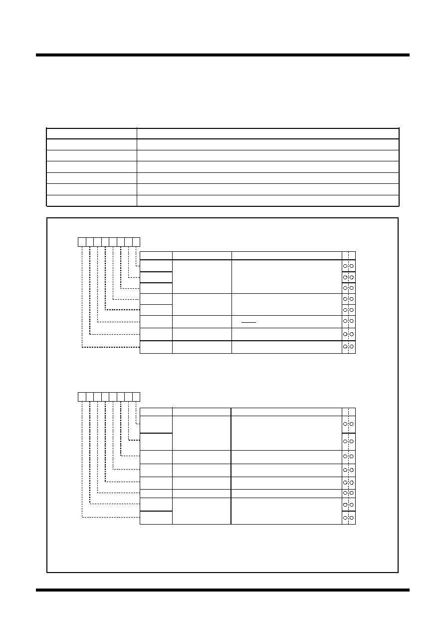
153
Tentative Specifications REV.A
Mitsubishi microcomputers
M16C / 62T Group
SINGLE-CHIP 16-BIT CMOS MICROCOMPUTER
S
pecifications in this manual are tentative and subject to change.
Under
development
A-D Converter
(4) Repeat sweep mode 0
In repeat sweep mode 0, the pins selected using the A-D sweep pin select bit are used for repeat sweep
A-D conversion. Table 1.20.5 shows the specifications of repeat sweep mode 0. Figure 1.20.7 shows the
A-D control register in repeat sweep mode 0.
Figure 1.20.7. A-D conversion register in repeat sweep mode 0
A-D control register 0
(Note 1)
Symbol
Address
When reset
ADCON0
03D6
16
00000XXX
2
b7
b6
b5
b4
b3
b2
b1
b0
Analog input pin select bit
CH0
Bit symbol
Bit name
Function
CH1
CH2
A-D operation mode
select bit 0
1 1 : Repeat sweep mode 0
MD0
MD1
Trigger select bit
0 : Software trigger
1 : AD
TRG
trigger
TRG
ADST
A-D conversion start flag
0 : A-D conversion disabled
1 : A-D conversion started
Frequency select bit 0
0 : f
AD
/4 is selected
1 : f
AD
/2 is selected
CKS0
W
R
A-D control register 1 (Note 1)
Symbol
Address
When reset
ADCON1
03D7
16
00
16
Bit name
Function
Bit symbol
b7
b6
b5
b4
b3
b2
b1
b0
A-D sweep pin select bit
SCAN0
SCAN1
MD2
BITS
8/10-bit mode select bit
0 : 8-bit mode
1 : 10-bit mode
VCUT
OPA0
Vref connect bit
0 : Any mode other than repeat sweep mode 1
OPA1
A-D operation mode
select bit 1
1 : Vref connected
External op-amp
connection mode
bit (Note 4)
W
R
1
1
Invalid in repeat sweep mode 0
0
Note 1: If the A-D control register is rewritten during A-D conversion, the conversion result
is indeterminate.
Note 2: Divide the frequency if f(X
IN
) exceeds 10MHz, and make
AD
frequency equal to
10MHz.
Note 3: AN
00
to AN
07
, and AN
20
to AN
27
can be used the same as AN
0
to AN
7
.
Note 4: Neither "01" nor "10" can be selected with the external op-amp connection mode bit.
b4 b3
When single sweep and repeat sweep mode 0
are selected
0 0 : AN
0
, AN
1
(2 pins)
0 1 : AN
0
to AN
3
(4 pins)
1 0 : AN
0
to AN
5
(6 pins)
1 1 : AN
0
to AN
7
(8 pins)
b1 b0
0 0 : ANEX0 and ANEX1 are not used
0 1 : ANEX0 input is A-D converted
1 0 : ANEX1 input is A-D converted
1 1 : External op-amp connection mode
b7 b6
1
Note 1: If the A-D control register is rewritten during A-D conversion, the conversion result
is indeterminate.
Frequency select bit 1
0 : f
AD
/2 or f
AD
/4 is selected
1 : f
AD
is selected
CKS1
(Note 2)
(Note 3)
Item
Specification
Function
The pins selected by the A-D sweep pin select bit are used for repeat sweep A-D conversion
Start condition
Writing "1" to A-D conversion start flag
Stop condition
Writing "0" to A-D conversion start flag
Interrupt request generation timing
None generated
Input pin
AN
0
and AN
1
(2 pins), AN
0
to AN
3
(4 pins), AN
0
to AN
5
(6 pins), or AN
0
to AN
7
(8 pins) (Note 1)
Reading of result of A-D converter
Read A-D register corresponding to selected pin (at any time)
Table 1.20.5. Repeat sweep mode 0 specifications
Note 1: AN
00
to AN
07
, and AN
20
to AN
27
can be used the same as AN
0
to AN
7
.
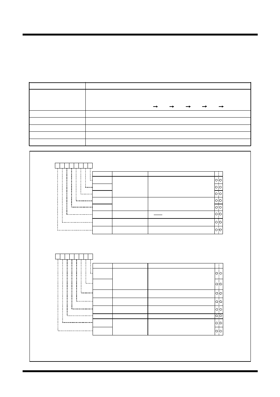
154
Tentative Specifications REV.A
Mitsubishi microcomputers
M16C / 62T Group
SINGLE-CHIP 16-BIT CMOS MICROCOMPUTER
S
pecifications in this manual are tentative and subject to change.
Under
development
A-D Converter
Item
Specification
Function
All pins perform repeat sweep A-D conversion, with emphasis on the pin or
pins selected by the A-D sweep pin select bit
Example : AN
0
selected AN
0
AN
1
AN
0
AN
2
AN
0
AN
3
, etc
Start condition
Writing "1" to A-D conversion start flag
Stop condition
Writing "0" to A-D conversion start flag
Interrupt request generation timing
None generated
Input pin
AN
0
(1 pin), AN
0
and AN
1
(2 pins), AN
0
to AN
2
(3 pins), AN
0
to AN
3
(4 pins) (Note1 )
Reading of result of A-D converter
Read A-D register corresponding to selected pin (at any time)
(5) Repeat sweep mode 1
In repeat sweep mode 1, all pins are used for A-D conversion with emphasis on the pin or pins selected
using the A-D sweep pin select bit. Table 1.20.6 shows the specifications of repeat sweep mode 1. Figure
1.20.8 shows the A-D control register in repeat sweep mode 1.
A-D control register 0
(Note 1)
Symbol
Address
When reset
ADCON0
03D6
16
00000XXX
2
b7
b6
b5
b4
b3
b2
b1
b0
Analog input pin select bit
CH0
Bit symbol
Bit name
Function
CH1
CH2
A-D operation mode
select bit 0
1 1 : Repeat sweep mode 1
MD0
MD1
Trigger select bit
0 : Software trigger
1 : AD
TRG
trigger
TRG
ADST
A-D conversion start flag
0 : A-D conversion disabled
1 : A-D conversion started
Frequency select bit 0
0 : f
AD
/4 is selected
1 : f
AD
/2 is selected
CKS0
W
R
A-D control register 1 (Note 1)
Symbol
Address
When reset
ADCON1
03D7
16
00
16
Bit name
Function
Bit symbol
b7
b6
b5
b4
b3
b2
b1
b0
A-D sweep pin select bit
SCAN0
SCAN1
MD2
BITS
8/10-bit mode select bit
0 : 8-bit mode
1 : 10-bit mode
VCUT
OPA0
Vref connect bit
1 : Repeat sweep mode 1
OPA1
A-D operation mode
select bit 1
1 : Vref connected
External op-amp
connection mode
bit (Note 4)
W
R
1 1
Invalid in repeat sweep mode 1
1
Note 1: If the A-D control register is rewritten during A-D conversion, the conversion result
is indeterminate.
Note 2: Divide the frequency if f(X
IN
) exceeds 10MHz, and make
AD
frequency equal to
10MHz.
Note 3: AN
00
to AN
07
, and AN
20
to AN
27
can be used the same as AN
0
to AN
7
.
Note 4: Neither `01' nor `10' can be selected with the external op-amp connection mode bit.
b4 b3
When repeat sweep mode 1 is selected
0 0 : AN
0
(1 pin)
0 1 : AN
0
, AN
1
(2 pins)
1 0 : AN
0
to AN
2
(3 pins)
1 1 : AN
0
to AN
3
(4 pins)
b1 b0
0 0 : ANEX0 and ANEX1 are not used
0 1 : ANEX0 input is A-D converted
1 0 : ANEX1 input is A-D converted
1 1 : External op-amp connection mode
b7 b6
1
Note 1: If the A-D control register is rewritten during A-D conversion, the conversion result
is indeterminate.
Frequency select bit 1
0 : f
AD
/2 or f
AD
/4 is selected
1 : f
AD
is selected
CKS1
(Note 2)
(Note 3)
Figure 1.20.8. A-D conversion register in repeat sweep mode 1
Table 1.20.6. Repeat sweep mode 1 specifications
Note 1: AN
00
to AN
07
, and AN
20
to AN
27
can be used the same as AN
0
to AN
7
.

155
Tentative Specifications REV.A
Mitsubishi microcomputers
M16C / 62T Group
SINGLE-CHIP 16-BIT CMOS MICROCOMPUTER
S
pecifications in this manual are tentative and subject to change.
Under
development
A-D Converter
(a) Sample and hold
Sample and hold is selected by setting bit 0 of the A-D control register 2 (address 03D4
16
) to "1". When
sample and hold is selected, the rate of conversion of each pin increases. As a result, a 28
AD
cycle is
achieved with 8-bit resolution and 33
AD
with 10-bit resolution. Sample and hold can be selected in all
modes. However, in all modes, be sure to specify before starting A-D conversion whether sample and
hold is to be used.
(b) Extended analog input pins
In one-shot mode and repeat mode, the input via the extended analog input pins ANEX0 and ANEX1 can
also be converted from analog to digital.
When bit 6 of the A-D control register 1 (address 03D7
16
) is "1" and bit 7 is "0", input via ANEX0 is
converted from analog to digital. The result of conversion is stored in A-D register 0.
When bit 6 of the A-D control register 1 (address 03D7
16
) is "0" and bit 7 is "1", input via ANEX1 is
converted from analog to digital. The result of conversion is stored in A-D register 1.
Furthermore, the input via 16pins of the extended analog input pins AN
00
to AN
07
,
AN
20
to AN
27
can be
converted from analog to digital. These pins can be used the same as AN
0
to AN
7
.
Use the A-D control register 2 (address 03D4
16
) bit 1 and bit 2 to select the pin group AN
0
to AN
7
, AN
00
to AN
07
,
AN
20
to AN
27
.
In the selected pin group, the pins is not used as the analog input pin, can be used as normal I/O ports, or
I/O pins of each peripheral function.
(c) External operation amp connection mode
In this mode, multiple external analog inputs via the extended analog input pins, ANEX0 and ANEX1, can
be amplified together by just one operation amp and used as the input for A-D conversion.
When bit 6 of the A-D control register 1 (address 03D7
16
) is "1" and bit 7 is "1", input via AN
0
to AN
7
(Note
1) is output from ANEX0. The input from ANEX1 is converted from analog to digital and the result stored
in the corresponding A-D register. The speed of A-D conversion depends on the response of the external
operation amp. Do not connect the ANEX0 and ANEX1 pins directly. Figure 1.20.9 is an example of how
to connect the pins in external operation amp mode.
Note 1: AN
00
to AN
07
,
AN
20
to AN
27
can be used the same as AN
0
to AN
7
.
(d) Caution of using A-D converter
(1) Set the direction register of the following ports to input: the port corresponding to a pin to be used as
an analog input pin and external trigger input pin(P9
7
).
(2) In using a key-input interrupt, none of 4 pins (AN
4
through AN
7)
can be used as an A-D conversion port
(if the A-D input voltage goes to ``L'' level, a key-input interrupt occurs).
(3) Insert the capacitor between AVcc and AVss, between V
REF
and AVss, and between the analog input
pin (AN
i
) and AVss, to prevent a malfunction or program runaway, and to reduce conversion error,
due to noise. Figure 1.20.10 is an example connection of each pin.
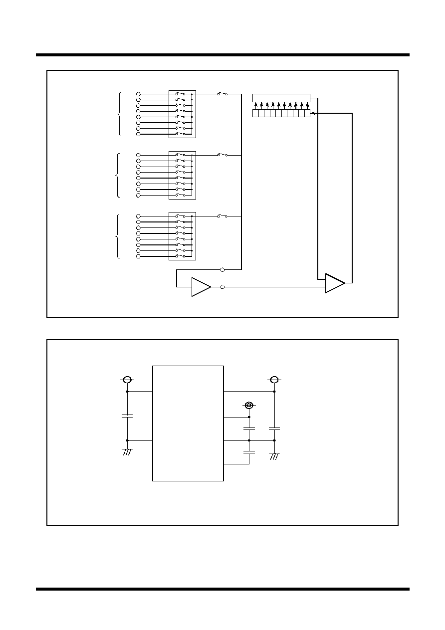
156
Tentative Specifications REV.A
Mitsubishi microcomputers
M16C / 62T Group
SINGLE-CHIP 16-BIT CMOS MICROCOMPUTER
S
pecifications in this manual are tentative and subject to change.
Under
development
A-D Converter
AN
0
AN
1
AN
2
AN
3
AN
4
AN
5
AN
6
AN
7
AN
00
AN
01
AN
02
AN
03
AN
04
AN
05
AN
06
AN
07
ADGSEL1,ADGSEL0
= 0,0
ADGSEL1,ADGSEL0
= 1,0
AN
20
AN
21
AN
22
AN
23
AN
24
AN
25
AN
26
AN
27
ADGSEL1,ADGSEL0
= 1,1
ANEX
0
ANEX
1
Analog input pins
Resistor ladder
Successive conversion register
External op-amp
Comparator
Port P10 group
Analog input pins
Port P0 group
Analog input pins
Port P2 group
V
C
C
A
V
C
C
V
S
S
A
V
S
S
A
N
i
C
4
C
1
C
3
C
2
V
R
E
F
M
i
c
r
o
c
o
m
p
u
t
e
r
N
o
t
e
1
:
C
1
0
.
4
7
µ
F
,
C
2
0
.
4
7
µ
F
,
C
3
1
0
0
p
F
,
C
4
0
.
1
µ
F
N
o
t
e
2
:
U
s
e
t
h
i
c
k
a
n
d
s
h
o
r
t
e
s
t
p
o
s
s
i
b
l
e
w
i
r
i
n
g
t
o
c
o
n
n
e
c
t
c
a
p
a
c
i
t
o
r
s
.
Figure 1.20.9. Example of external op-amp connection mode
Figure 1.20.10. Example connection of V
CC
, V
SS
, AV
CC
, AV
SS
, V
REF
and AN
i
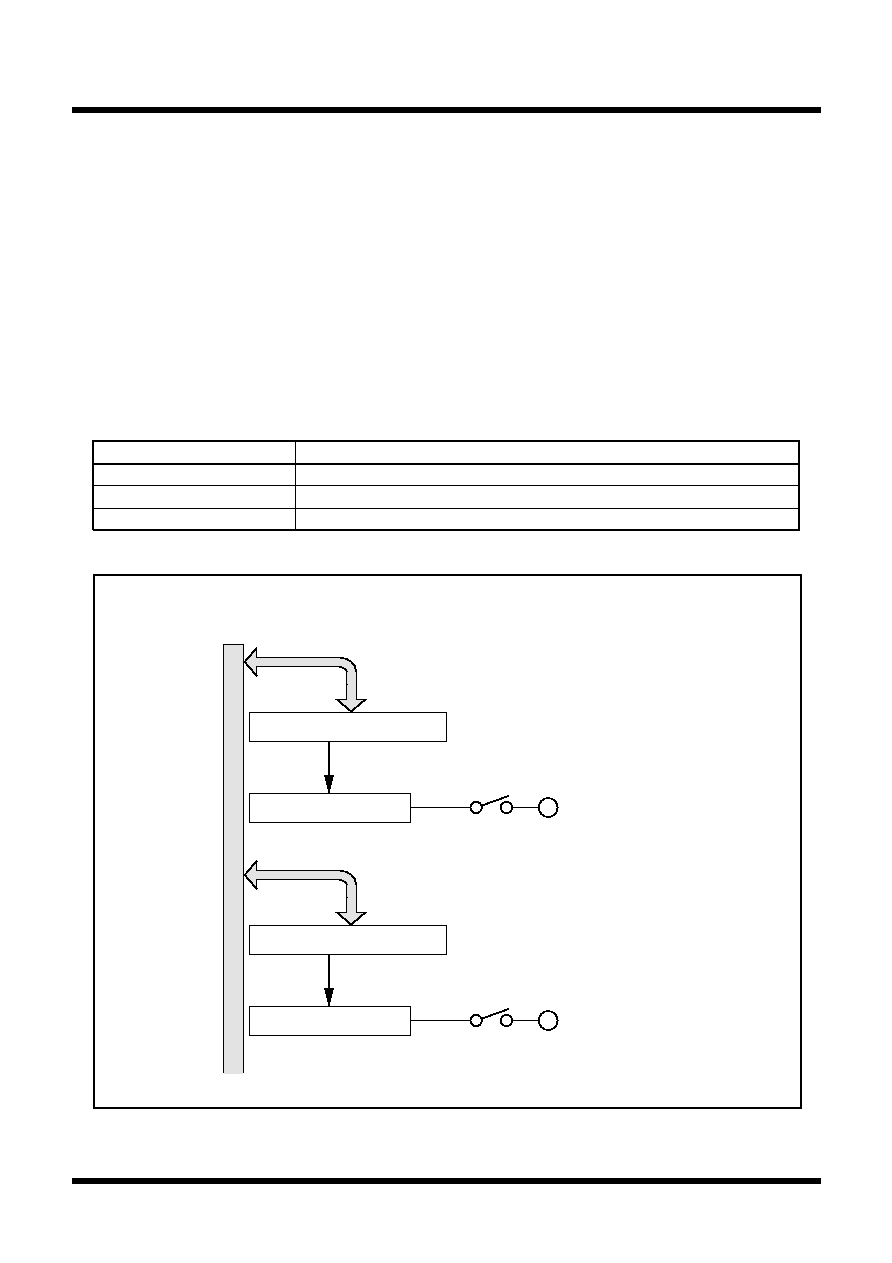
157
Tentative Specifications REV.A
Mitsubishi microcomputers
M16C / 62T Group
SINGLE-CHIP 16-BIT CMOS MICROCOMPUTER
S
pecifications in this manual are tentative and subject to change.
Under
development
D-A Converter
D-A Converter
This is an 8-bit, R-2R type D-A converter. The microcomputer contains two independent D-A converters of
this type.
D-A conversion is performed when a value is written to the corresponding D-A register. Bits 0 and 1 (D-A
output enable bits) of the D-A control register decide if the result of conversion is to be output. Do not set the
target port to output mode if D-A conversion is to be performed.
Output analog voltage (V) is determined by a set value (n : decimal) in the D-A register.
V = V
REF
X n/ 256 (n = 0 to 255)
V
REF
: reference voltage
Table 1.21.1 lists the performance of the D-A converter. Figure 1.21.1 shows the block diagram of the D-A
converter. Figure 1.21.2 shows the D-A control register. Figure 1.21.3 shows the D-A converter equivalent
circuit.
Item
Performance
Conversion method
R-2R method
Resolution
8 bits
Analog output pin
2 channels
Table 1.21.1. Performance of D-A converter
P9
3
/DA
0
P9
4
/DA
1
Data bus low-order bits
D-A register0 (8)
R-2R resistor ladder
D-A0 output enable bit
D-A register1 (8)
R-2R resistor ladder
D-A1 output enable bit
(Address 03D8
16
)
(Address 03DA
16
)
Figure 1.21.1. Block diagram of D-A converter
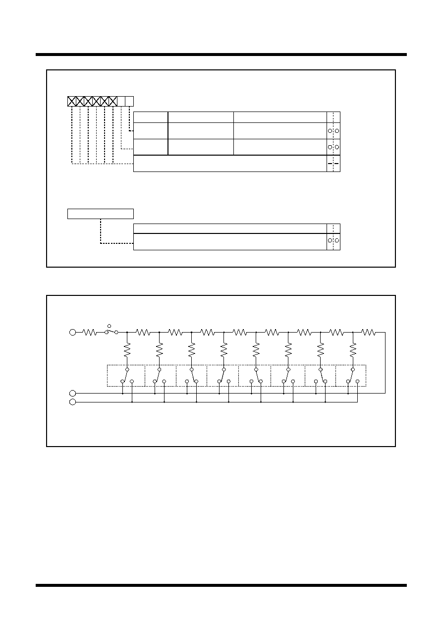
158
Tentative Specifications REV.A
Mitsubishi microcomputers
M16C / 62T Group
SINGLE-CHIP 16-BIT CMOS MICROCOMPUTER
S
pecifications in this manual are tentative and subject to change.
Under
development
D-A Converter
Figure 1.21.2. D-A control register
D-A control register
Symbol
Address
When reset
DACON
03DC
16
00
16
b7
b6
b5
b4
b3
b2
b1
b0
D-A0 output enable bit
DA0E
Bit symbol
Bit name
Function
R W
0 : Output disabled
1 : Output enabled
D-A1 output enable bit
0 : Output disabled
1 : Output enabled
DA1E
Nothing is assigned.
In an attempt to write to these bits, write "0". The value, if read, turns out to be "0"
D-A register
Symbol
Address
When reset
DAi (i = 0,1)
03D8
16
,
03DA
16
Indeterminate
W
R
b7
b0
Function
R W
Output value of D-A conversion
V
REF
AV
SS
2R
R
2R
R
2R
R
2R
R
2R
R
2R
R
2R
R
2R
2R
DA0
MSB
LSB
D-A0 output enable bit
"0"
"1"
D-A0 register0
Note 1: The above diagram shows an instance in which the D-A register is assigned 2A
16
.
Note 2: The same circuit as this is also used for D-A1.
Note 3: To reduce the current consumption when the D-A converter is not used, set the D-A output enable bit to 0
and set the D-A register to 00
16
so that no current flows in the resistors Rs and 2Rs.
Figure 1.21.3. D-A converter equivalent circuit
159
Tentative Specifications REV.A
Mitsubishi microcomputers
M16C / 62T Group
SINGLE-CHIP 16-BIT CMOS MICROCOMPUTER
S
pecifications in this manual are tentative and subject to change.
Under
development
CRC
CRC Calculation Circuit
The Cyclic Redundancy Check (CRC) calculation circuit detects an error in data blocks. The microcom-
puter uses a generator polynomial of CRC_CCITT (X
16
+ X
12
+ X
5
+ 1) to generate CRC code.
The CRC code is a 16-bit code generated for a block of a given data length in multiples of 8 bits. The CRC
code is set in a CRC data register each time one byte of data is transferred to a CRC input register after
writing an initial value into the CRC data register. Generation of CRC code for one byte of data is com-
pleted in two machine cycles.
Figure 1.22.1 shows the block diagram of the CRC circuit. Figure 1.22.2 shows the CRC-related registers.
Figure 1.22.3 shows the calculation example using the CRC calculation circuit
Figure 1.22.2. CRC-related registers
Symbol
Address
When reset
CRCD
03BD
16
, 03BC
16
Indeterminate
b7
b0 b7
b0
(b15)
(b8)
CRC data register
W
R
CRC calculation result output register
Function
Values that
can be set
0000
16
to FFFF
16
Symbo
Address
When reset
CRCIN
03BE
16
Indeterminate
b7
b0
CRC input register
W
R
Data input register
Function
Values that
can be set
00
16
to FF
16
Eight low-order bits
Eight high-order bits
Data bus high-order bits
Data bus low-order bits
CRC data register (16)
CRC input register (8)
CRC code generating circuit
x
16
+ x
12
+ x
5
+ 1
(Addresses 03BD
16
, 03BC
16
)
(Address 03BE
16
)
Figure 1.22.1. Block diagram of CRC circuit
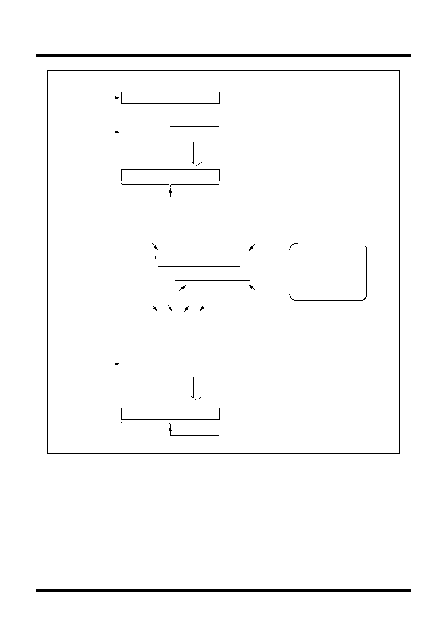
160
Tentative Specifications REV.A
Mitsubishi microcomputers
M16C / 62T Group
SINGLE-CHIP 16-BIT CMOS MICROCOMPUTER
S
pecifications in this manual are tentative and subject to change.
Under
development
CRC
b15
b0
(1) Setting 0000
16
CRC data register
CRCD
[03BD
16
, 03BC
16
]
b0
b7
b15
b0
(2) Setting 01
16
CRC input register
CRCIN
[03BE
16
]
2 cycles
After CRC calculation is complete
CRC data register
CRCD
[03BD
16
, 03BC
16
]
1189
16
Stores CRC code
b0
b7
b15
b0
(3) Setting 23
16
CRC input register
CRCIN
[03BE
16
]
After CRC calculation is complete
CRC data register
CRCD
[03BD
16
, 03BC
16
]
0A41
16
Stores CRC code
The code resulting from sending 01
16
in LSB first mode is (1000 0000). Thus the CRC code in the generating polynomial,
(X
16
+ X
12
+ X
5
+ 1), becomes the remainder resulting from dividing (1000 0000) X
16
by (1 0001 0000 0010 0001) in
conformity with the modulo-2 operation.
Thus the CRC code becomes (1001 0001 1000 1000). Since the operation is in LSB first mode, the (1001 0001 1000 1000)
corresponds to 1189
16
in hexadecimal notation. If the CRC operation in MSB first mode is necessary in the CRC operation
circuit built in the M16C, switch between the LSB side and the MSB side of the input-holding bits, and carry out the CRC
operation. Also switch between the MSB and LSB of the result as stored in CRC data.
1 0001 0000 0010 0001
1000 0000 0000 0000 0000 0000
1000 1000 0001 0000 1
1000 0001 0000 1000 0
1000 1000 0001 0000 1
1001 0001 1000 1000
1000 1000
LSB
MSB
LSB
MSB
9
8
1
1
Modulo-2 operation is
operation that complies
with the law given below.
0 + 0 = 0
0 + 1 = 1
1 + 0 = 1
1 + 1 = 0
-1 = 1
Figure 1.22.3. Calculation example using the CRC calculation circuit

161
Tentative Specifications REV.A
Mitsubishi microcomputers
M16C / 62T Group
SINGLE-CHIP 16-BIT CMOS MICROCOMPUTER
S
pecifications in this manual are tentative and subject to change.
Under
development
Programmable I/O Port
Programmable I/O Ports
M30622(100-pin package) has 87 programmable I/O ports: P0 to P10 (excluding P8
5
). M30623(80-pin
package) has 70 (P1, P4
4
to P4
7
,
P7
2
to P7
5
, P9
1
are not connected to external pin).
Each port can be set independently for input or output using the direction register. A pull-up resistance for
each block of 4 ports can be set. P8
5
is an input-only port and has no built-in pull-up resistance.
Figures 1.23.1 to 1.23.3 show the programmable I/O ports. Figure 1.23.4 shows the I/O pins.
Each pin functions as a programmable I/O port and as the I/O for the built-in peripheral devices.
To use the pins as the inputs for the built-in peripheral devices, set the direction register of each pin to input
mode. When the pins are used as the outputs for the built-in peripheral devices (other than the D-A con-
verter), they function as outputs regardless of the contents of the direction registers. When pins are to be
used as the outputs for the D-A converter, do not set the direction registers to output mode. See the
descriptions of the respective functions for how to set up the built-in peripheral devices.
(1) Direction registers
Figure 1.23.5 shows the direction registers.
These registers are used to choose the direction of the programmable I/O ports. Each bit in these regis-
ters corresponds one for one to each I/O pin.
Note: There is no direction register bit for P8
5
.
(2) Port registers
Figure 1.23.6 shows the port registers.
These registers are used to write and read data for input and output to and from an external device. A
port register consists of a port latch to hold output data and a circuit to read the status of a pin. Each bit
in port registers corresponds one for one to each I/O pin.
(3) Pull-up control registers
Figure 1.23.7 shows the pull-up control registers.
The pull-up control register can be set to apply a pull-up resistance to each block of 4 ports. When ports
are set to have a pull-up resistance, the pull-up resistance is connected only when the direction register is
set for input.
However, in memory expansion mode and microprocessor mode, P0 to P5 operate as the bus and the
pull-up control register setting is invalid.
(4) Port control register
Figure 1.23.8 shows the port control register.
The bit 0 of port control resister is used to read port P1 as follows:
0 : When port P1 is input port, port input level is read.
When port P1 is output port , the contents of port P1 register is read.
1 : The contents of port P1 register is read always.
This register is valid in the following:
· External bus width is 8 bits in microprocessor mode or memory expansion mode.
· Port P1 can be used as a port in multiplexed bus for the entire space.
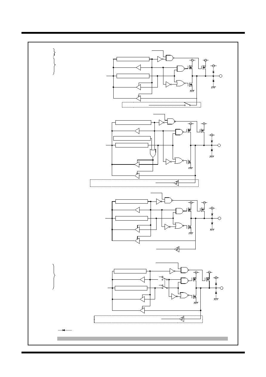
162
Tentative Specifications REV.A
Mitsubishi microcomputers
M16C / 62T Group
SINGLE-CHIP 16-BIT CMOS MICROCOMPUTER
S
pecifications in this manual are tentative and subject to change.
Under
development
Programmable I/O Port
Figure 1.23.1. Programmable I/O ports (1)
P0
0
to P0
7
,
P2
0
to P2
7
P1
0
to P1
4
(inside dotted-line not included)
P1
5
to P1
7
(inside dotted-line included)
Note 1: symbolizes a parasitic diode.
Do not apply a voltage higher than Vcc to each port.
Note 2: In M30623(80-pin package), P1
0
to P1
7
, P4
4
to P4
7
, P7
2
to P7
5
, and P9
1
are not connected to external pin.
Direction register
Port latch
Pull-up selection
Data bus
Input to respective peripheral functions
"1"
Output
(Note 1)
Data bus
Direction register
Pull-up selection
Port latch
(Note 1)
Pull-up selection
Data bus
Direction register
Pull-up selection
Port latch
(Note 1)
Input to respective peripheral functions
P3
0
to P3
7
,
P4
0
to P4
7
,
P5
0
to P5
4
,
P5
6
P5
7
,
P6
0
, P6
1
,
P6
4
, P6
5
,
P7
2
to P7
6
,
P8
0
, P8
1
,
P9
0
, P9
2
P5
5
,
P6
2
, P6
6
,
P7
7
,
P9
1
, P9
7
P6
3
, P6
7
(inside dotted-line not included)
Direction register
Port latch
Port P1 control register
Data bus
Input to respective peripheral functions
(Note 1)
Analog Input
inside dotted-line
included
inside dotted-line
not included
inside dotted-line
included
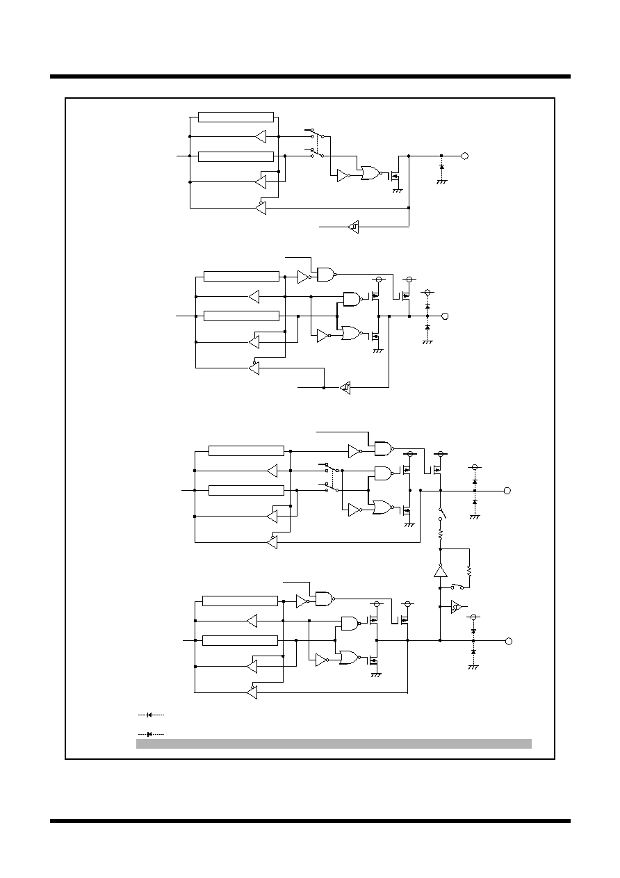
163
Tentative Specifications REV.A
Mitsubishi microcomputers
M16C / 62T Group
SINGLE-CHIP 16-BIT CMOS MICROCOMPUTER
S
pecifications in this manual are tentative and subject to change.
Under
development
Programmable I/O Port
Figure 1.23.2. Programmable I/O ports (2)
P8
2
to P8
4
Data bus
Direction register
Pull-up selection
Port latch
Input to respective peripheral functions
(Note 1)
P7
0
, P7
1
P8
6
P8
7
"1"
Output
Direction register
Pull-up selection
Port latch
Data bus
(Note 1)
Data bus
Direction register
Pull-up selection
Port latch
(Note 1)
Rf
fc
Rd
"1"
Output
Direction register
Port latch
Input to respective peripheral functions
(Note 2)
Data bus
Note 1: symbolizes a parasitic diode.
Do not apply a voltage higher than Vcc to each port.
Note 2: symbolizes a parasitic diode.
Note 3: In M30623(80-pin package), P1
0
to P1
7
, P4
4
to P4
7
, P7
2
to P7
5
, and P9
1
are not connected to external pin.
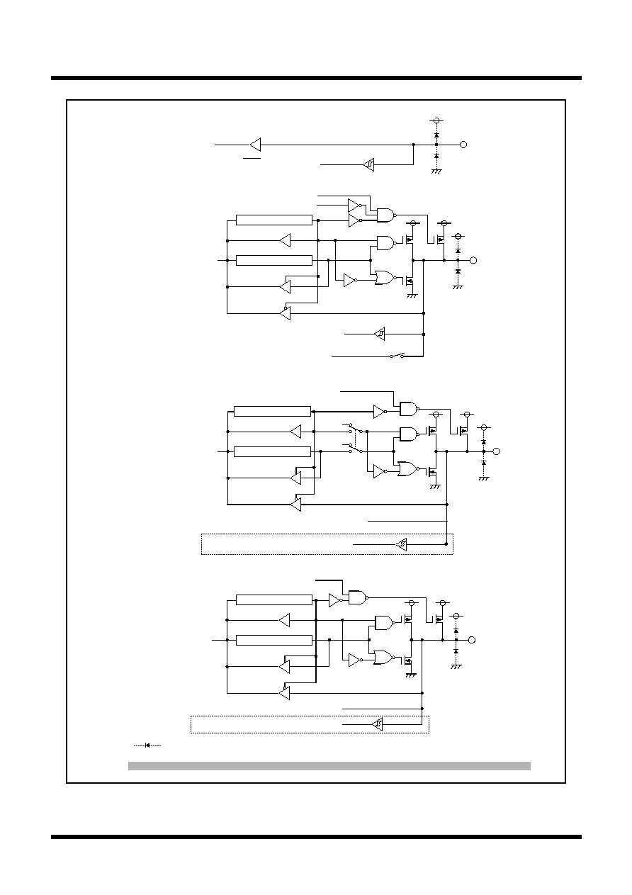
164
Tentative Specifications REV.A
Mitsubishi microcomputers
M16C / 62T Group
SINGLE-CHIP 16-BIT CMOS MICROCOMPUTER
S
pecifications in this manual are tentative and subject to change.
Under
development
Programmable I/O Port
Figure 1.23.3. Programmable I/O ports (3)
P9
3
, P9
4
P10
0
to P10
3
(inside dotted-line not included)
P10
4
to P10
7
(inside dotted-line included)
Data bus
Direction register
Pull-up selection
Port latch
Analog input
Input to respective peripheral functions
(Note 1)
D-A output enabled
Direction register
Pull-up selection
Port latch
Data bus
Input to respective peripheral functions
D-A output enabled
Analog output
(Note 1)
P9
5
(inside dotted-line included)
P8
5
Data bus
NMI interrupt input
(Note 1)
P9
6
(inside dotted-line not included)
"1"
Output
Direction register
Pull-up selection
Port latch
Data bus
Analog input
Input to respective peripheral functions
(Note 1)
Note 1: symbolizes a parasitic diode.
Do not apply a voltage higher than Vcc to each port.
Note 2: In M30623(80-pin package), P1
0
to P1
7
, P4
4
to P4
7
, P7
2
to P7
5
, and P9
1
are not connected to external pin.
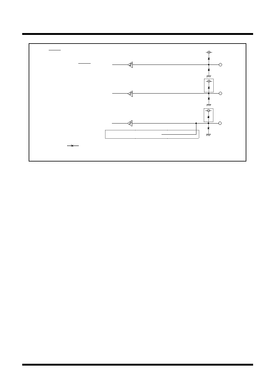
165
Tentative Specifications REV.A
Mitsubishi microcomputers
M16C / 62T Group
SINGLE-CHIP 16-BIT CMOS MICROCOMPUTER
S
pecifications in this manual are tentative and subject to change.
Under
development
Programmable I/O Port
Figure 1.23.4. I/O pins
Note 1: symbolizes a parasitic diode.
Do not apply a voltage higher than Vcc to each pin.
BYTE
BYTE signal input
(Note 1)
CNV
SS
CNV
SS
signal input
(Note 1)
RESET
RESET signal input
(Note 1)
Mask ROM version(inside dotted-line not included)
Onetime PROM version(inside dotted-line included)
To circuit of PROM-programming
166
Tentative Specifications REV.A
Mitsubishi microcomputers
M16C / 62T Group
SINGLE-CHIP 16-BIT CMOS MICROCOMPUTER
S
pecifications in this manual are tentative and subject to change.
Under
development
Programmable I/O Port
Figure 1.23.5. Direction register
Port Pi direction register (Note 1)
Symbol
Address
When reset
PDi (i = 0 to 10, except 8)
03E2
16
, 03E3
16
, 03E6
16
, 03E7
16
, 03EA
16
00
16
03EB
16
, 03EE
16
, 03EF
16
, 03F3
16
, 03F6
16
Bit name
Function
Bit symbol
W
R
b7
b6
b5
b4
b3
b2
b1
b0
PDi_0
Port Pi
0
direction register
PDi_1
Port Pi
1
direction register
PDi_2
Port Pi
2
direction register
PDi_3
Port Pi
3
direction register
PDi_4
Port Pi
4
direction register
PDi_5
Port Pi
5
direction register
PDi_6
Port Pi
6
direction register
PDi_7
Port Pi
7
direction register
0 : Input mode
(Functions as an input port)
1 : Output mode
(Functions as an output port)
(i = 0 to 10 except 8)
Port P8 direction register
Symbol
Address
When reset
PD8
03F2
16
00X00000
2
Bit name
Function
Bit symbol
W
R
b7
b6
b5
b4
b3
b2
b1
b0
PD8_0
Port P8
0
direction register
PD8_1
Port P8
1
direction register
PD8_2
Port P8
2
direction register
PD8_3
Port P8
3
direction register
PD8_4
Port P8
4
direction register
Nothing is assigned.
In an attempt to write to this bit, write "0". The value, if read, turns out to be
indeterminate.
PD8_6
Port P8
6
direction register
PD8_7
Port P8
7
direction register
0 : Input mode
(Functions as an input port)
1 : Output mode
(Functions as an output port)
0 : Input mode
(Functions as an input port)
1 : Output mode
(Functions as an output port)
Note 1: Set bit 2 of protect register (address 000A
16
) to "1" before rewriting to
the port P9 direction register.
Note 2: In M30623(80-pin package), P1, P4
4
to P4
7
, P7
2
to P7
5
, and P9
1
are
not connected to external pin, But exist inside microcomputer. So set
these ports for output mode.
167
Tentative Specifications REV.A
Mitsubishi microcomputers
M16C / 62T Group
SINGLE-CHIP 16-BIT CMOS MICROCOMPUTER
S
pecifications in this manual are tentative and subject to change.
Under
development
Programmable I/O Port
Figure 1.23.6. Port register
Port Pi register
Symbol
Address
When reset
Pi (i = 0 to 10, except 8)
03E0
16
, 03E1
16
, 03E4
16
, 03E5
16
, 03E8
16
Indeterminate
03E9
16
, 03EC
16
, 03ED
16
, 03F1
16
, 03F4
16
Indeterminate
Bit name
Function
Bit symbol
W
R
b7
b6
b5
b4
b3
b2
b1
b0
Pi_0
Port Pi
0
register
Pi_1
Port Pi
1
register
Pi_2
Port Pi
2
register
Pi_3
Port Pi
3
register
Pi_4
Port Pi
4
register
Pi_5
Port Pi
5
register
Pi_6
Port Pi
6
register
Pi_7
Port Pi
7
register
Data is input and output to and from
each pin by reading and writing to
and from each corresponding bit
0 : "L" level data
1 : "H" level data (Note)
(i = 0 to 10 except 8)
Port P8 register
Symbol
Address
When reset
P8
03F0
16
Indeterminate
Bit name
Function
Bit symbol
W
R
b7
b6
b5
b4
b3
b2
b1
b0
P8_0
Port P8
0
register
P8_1
Port P8
1
register
P8_2
Port P8
2
register
P8_3
Port P8
3
register
P8_4
Port P8
4
register
P8_5
Port P8
5
register
P8_6
Port P8
6
register
P8_7
Port P8
7
register
Data is input and output to and from
each pin by reading and writing to
and from each corresponding bit
(except for P8
5
)
0 : "L" level data
1 : "H" level data
Note 1: Since P7
0
and P7
1
are N-channel open drain ports, the data is high-impedance.
Note 2: In M30623(80-pin package), P1, P4
4
to P4
7
, P7
2
to P7
5
, and P9
1
are not connected
to external pin, But exist inside microcomputer. So set these ports for output mode.
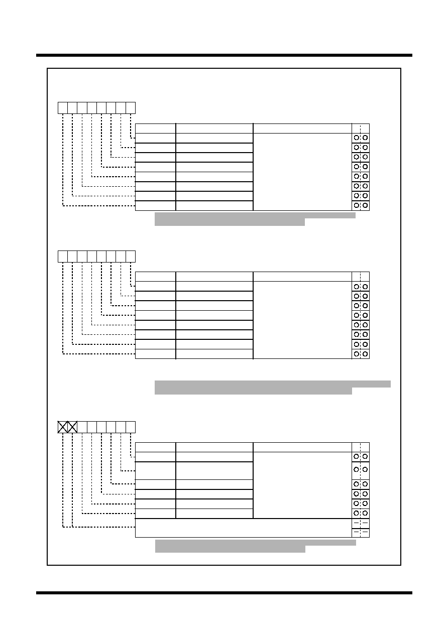
168
Tentative Specifications REV.A
Mitsubishi microcomputers
M16C / 62T Group
SINGLE-CHIP 16-BIT CMOS MICROCOMPUTER
S
pecifications in this manual are tentative and subject to change.
Under
development
Programmable I/O Port
Figure 1.23.7. Pull-up control register
Pull-up control register 0
Symbol
Address
When reset
PUR0
03FC
16
00
16
Bit name
Function
Bit symbol
W
R
b7
b6
b5
b4
b3
b2
b1
b0
PU00
P0
0
to P0
3
pull-up
PU01
P0
4
to P0
7
pull-up
PU02
P1
0
to P1
3
pull-up
PU03
P1
4
to P1
7
pull-up
PU04
P2
0
to P2
3
pull-up
PU05
P2
4
to P2
7
pull-up
PU06
P3
0
to P3
3
pull-up
PU07
P3
4
to P3
7
pull-up
The corresponding port is pulled
high with a pull-up resistor
0 : Not pulled high
1 : Pulled high
Pull-up control register 1
Symbol
Address
When reset
PUR1
03FD
16
00
16
(Note 2)
Bit name
Function
Bit symbol
W
R
b7
b6
b5
b4
b3
b2
b1
b0
PU10
P4
0
to P4
3
pull-up
PU11
P4
4
to P4
7
pull-up
PU12
P5
0
to P5
3
pull-up
PU13
P5
4
to P5
7
pull-up
PU14
P6
0
to P6
3
pull-up
PU15
P6
4
to P6
7
pull-up
PU16
P7
0
to P7
3
pull-up (Note 1)
PU17
P7
4
to P7
7
pull-up
The corresponding port is pulled
high with a pull-up resistor
0 : Not pulled high
1 : Pulled high
Note 1: Since P7
0
and P7
1
are N-channel open drain ports, pull-up is not available for them.
Note 2: When the V
CC
level is being impressed to the CNV
SS
terminal, this register becomes
to 02
16
when reset (PU11 becomes to "1").
Note 3: In M30623(80-pin package), P4
4
to P4
7
, and P7
2
to P7
5
are not connected to external
pin, but exist inside microcomputer. So set these ports for output mode.
Pull-up control register 2
Symbol
Address
When reset
PUR2
03FE
16
00
16
Bit name
Function
Bit symbol
W
R
b7
b6
b5
b4
b3
b2
b1
b0
PU20
P8
0
to P8
3
pull-up
PU21
P8
4
to P8
7
pull-up
(Except P8
5
)
PU22
P9
0
to P9
3
pull-up
PU23
P9
4
to P9
7
pull-up
PU24
P10
0
to P10
3
pull-up
PU25
P10
4
to P10
7
pull-up
Nothing is assigned.
In an attempt to write to these bits, write "0". The value, if read, turns out to be "0".
The corresponding port is pulled
high with a pull-up resistor
0 : Not pulled high
1 : Pulled high
Note 1: In M30623(80-pin package), P1 is not connected to external pin, but exist
inside microcomputer. so set this port for output mode.
Note 1: In M30623(80-pin package), P1 is not connected to external pin, but exist
inside microcomputer. so set this port for output mode.
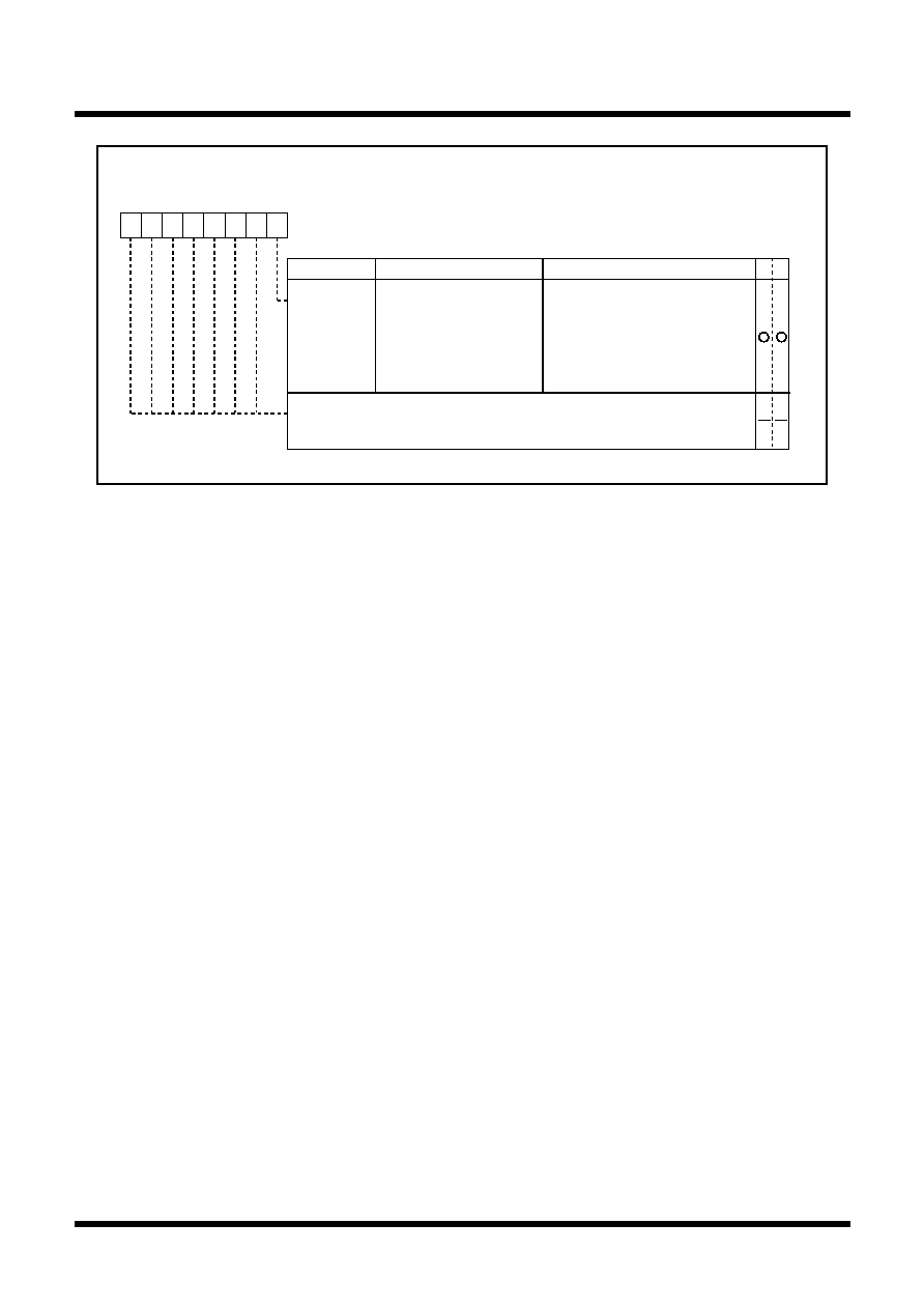
169
Tentative Specifications REV.A
Mitsubishi microcomputers
M16C / 62T Group
SINGLE-CHIP 16-BIT CMOS MICROCOMPUTER
S
pecifications in this manual are tentative and subject to change.
Under
development
Programmable I/O Port
Figure 1.23.8. Port control register
Port control register
Symbpl
Address
When reset
PCR
03FF
16
00
16
Bit name
Function
Bit symbol
W
R
b7
b6
b5
b4
b3
b2
b1
b0
PCR0
Port P1 control register
0 : When input port, read port
input level. When output port,
read the contents of port P1
register.
1 : Read the contents of port P1
register though input/output
port.
Nothing is assigned.
In an attempt to write to these bits, write "0". The value, if read, turns
out to be "0".
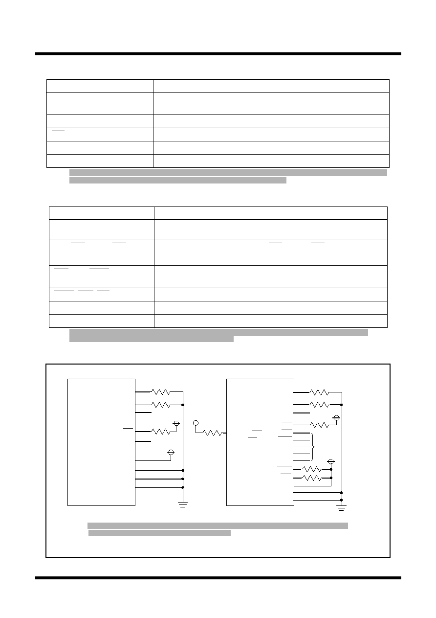
170
Tentative Specifications REV.A
Mitsubishi microcomputers
M16C / 62T Group
SINGLE-CHIP 16-BIT CMOS MICROCOMPUTER
S
pecifications in this manual are tentative and subject to change.
Under
development
Programmable I/O Port
Pin name
Connection
Ports P0 to P10
(excluding P8
5
) (Note 1)
X
OUT
(Note 2)
AV
SS
, V
REF
, BYTE
AV
CC
After setting for input mode, connect every pin to V
SS
or V
CC
via a
resistor; or after setting for output mode, leave these pins open.
Open
Connect to V
CC
Connect to V
SS
Note 1: In M30623(80-pin package), P1, P4
4
to P4
7
, P7
2
to P7
5
, and P9
1
are not connected to external pin,
but exist inside microcomputer. So set these ports for output mode.
Note 2: With external clock input to X
IN
pin.
NMI
Connect via resistor to V
CC
(pull-up)
Table 1.23.1. Example connection of unused pins in single-chip mode
Pin name
Connection
Ports P6 to P10
(excluding P8
5
) (Note 1)
AV
SS
, V
REF
AV
CC
After setting for input mode, connect every pin to V
SS
or V
CC
via a
resistor; or after setting for output mode, leave these pins open.
Open
Connect to V
CC
Connect to V
SS
Note 1: In M30623(80-pin package), P7
2
to P7
5
, P9
1
are not connected to external pin, but exist inside
microcomputer. So set these ports for output mode.
Note 2: With external clock input to X
IN
pin.
Note 3: The M16C/62T group is not guaranteed to operate in memory expansion and microprocessor modes.
HOLD, RDY, NMI
Connect via resistor to V
CC
(pull-up)
BHE, ALE, HLDA,
X
OUT
(Note 2), BCLK
P4
5
/ CS1 to P4
7
/ CS3
Sets ports to input mode, sets bits CS1 through CS3 to 0, and connects
to Vcc via resistors (pull-up).
Figure 1.23.9. Example connection of unused pins
Port P0 to P10 (except for P8
5
)
(Input mode)
·
·
·
(Input mode)
(Output mode)
NMI
X
OUT
AV
CC
BYTE
AV
SS
V
REF
Microcomputer
V
CC
V
SS
In single-chip mode
Port P6 to P10 (except for P8
5
)
(Input mode)
·
·
·
(Input mode)
(Output mode)
NMI
X
OUT
AV
CC
AV
SS
V
REF
Open
Microcomputer
V
CC
V
SS
In memory expansion mode or
in microprocessor mode
HOLD
RDY
ALE
BCLK
BHE
HLDA
Open
Open
Open
·
·
·
·
·
·
Port P4
5
/ CS1
to P4
7
/ CS3
Note 1: In M30623(80-pin package), P7
2
to P7
5
, P9
1
are not connected to external pin, but exist inside
microcomputer. So set these ports for output mode.
Note 2: The M16C/62T group is not guaranteed to operate in memory expansion and microprocessor modes.
Note 3: When the wiring between NMI and V
CC
is long, pull-up via resistor.
Table 1.23.2. Example connection of unused pins in memory expansion mode and microprocessor mode

171
Tentative Specifications REV.A
Mitsubishi microcomputers
M16C / 62T Group
SINGLE-CHIP 16-BIT CMOS MICROCOMPUTER
S
pecifications in this manual are tentative and subject to change.
Under
development
Usage precaution
Timer A (timer mode)
Usage Precaution
Timer A (event counter mode)
(1) Reading the timer Ai register while a count is in progress allows reading, with arbitrary timing, the
value of the counter. Reading the timer Ai register with the reload timing gets "FFFF
16
" by underflow
or "0000
16
" by overflow. Reading the timer Ai register after setting a value in the timer Ai register with
a count halted but before the counter starts counting gets a proper value.
(2) When stop counting in free run type, set timer again.
(1) Reading the timer Ai register while a count is in progress allows reading, with arbitrary timing, the
value of the counter. Reading the timer Ai register with the reload timing gets "FFFF
16
". Reading the
timer Ai register after setting a value in the timer Ai register with a count halted but before the counter
starts counting gets a proper value.
(1) Setting the count start flag to "0" while a count is in progress causes as follows:
· The counter stops counting and a content of reload register is reloaded.
· The TAi
OUT
pin outputs "L" level.
· The interrupt request generated and the timer Ai interrupt request bit goes to "1".
(2) The timer Ai interrupt request bit goes to "1" if the timer's operation mode is set using any of the
following procedures:
· Selecting one-shot timer mode after reset.
· Changing operation mode from timer mode to one-shot timer mode.
· Changing operation mode from event counter mode to one-shot timer mode.
Therefore, to use timer Ai interrupt (interrupt request bit), set timer Ai interrupt request bit to "0"
after the above listed changes have been made.
Timer A (one-shot timer mode)
(1) The timer Ai interrupt request bit becomes "1" if setting operation mode of the timer in compliance with
any of the following procedures:
· Selecting PWM mode after reset.
· Changing operation mode from timer mode to PWM mode.
· Changing operation mode from event counter mode to PWM mode.
Therefore, to use timer Ai interrupt (interrupt request bit), set timer Ai interrupt request bit to "0"
after the above listed changes have been made.
(2) Setting the count start flag to "0" while PWM pulses are being output causes the counter to stop
counting. If the TAi
OUT
pin is outputting an "H" level in this instance, the output level goes to "L", and
the timer Ai interrupt request bit goes to "1". If the TAi
OUT
pin is outputting an "L" level in this instance,
the level does not change, and the timer Ai interrupt request bit does not becomes "1".
Timer A (pulse width modulation mode)
Timer B (timer mode, event counter mode)
(1) Reading the timer Bi register while a count is in progress allows reading , with arbitrary timing, the
value of the counter. Reading the timer Bi register with the reload timing gets "FFFF
16
". Reading the
timer Bi register after setting a value in the timer Bi register with a count halted but before the counter
starts counting gets a proper value.

172
Tentative Specifications REV.A
Mitsubishi microcomputers
M16C / 62T Group
SINGLE-CHIP 16-BIT CMOS MICROCOMPUTER
S
pecifications in this manual are tentative and subject to change.
Under
development
Usage precaution
Stop Mode and Wait Mode
A-D Converter
(1) If changing the measurement mode select bit is set after a count is started, the timer Bi interrupt
request bit goes to "1".
(2) When the first effective edge is input after a count is started, an indeterminate value is transferred to
the reload register. At this time, timer Bi interrupt request is not generated.
Timer B (pulse period/pulse width measurement mode)
Interrupts
(1) Write to each bit (except bit 6) of A-D control register 0, to each bit of A-D control register 1, and to bit
0 of A-D control register 2 when A-D conversion is stopped (before a trigger occurs).
In particular, when the Vref connection bit is changed from "0" to "1", start A-D conversion after an
elapse of 1
µ
s or longer.
(2) When changing A-D operation mode, select analog input pin again.
(3) Using one-shot mode or single sweep mode
Read the correspondence A-D register after confirming A-D conversion is finished. (It is known by A-
D conversion interrupt request bit.)
(4) Using repeat mode, repeat sweep mode 0 or repeat sweep mode 1
Use the undivided main clock as the internal CPU clock.
(1) Reading address 00000
16
· When maskable interrupt is occurred, CPU read the interrupt information (the interrupt number
and interrupt request level) in the interrupt sequence.
The interrupt request bit of the certain interrupt written in address 00000
16
will then be set to "0".
Reading address 00000
16
by software sets enabled highest priority interrupt source request bit to "0".
Though the interrupt is generated, the interrupt routine may not be executed.
Do not read address 00000
16
by software.
(2) Setting the stack pointer
· The value of the stack pointer immediately after reset is initialized to 0000
16
. Accepting an
interrupt before setting a value in the stack pointer may become a factor of runaway. Be sure to
set a value in the stack pointer before accepting an interrupt.
_______
When using the NMI interrupt, initialize the stack point at the beginning of a program. Concerning
_______
the first instruction immediately after reset, generating any interrupts including the NMI interrupt is
prohibited.
_______
(3) The NMI interrupt
_______
· As for the NMI interrupt pin, an interrupt cannot be disabled. Connect it to the V
CC
pin via a
resistor (pull-up) if unused. Be sure to work on it.
_______
· Do not get either into stop mode with the NMI pin set to "L".
____________
(1) When returning from stop mode by hardware reset, RESET pin must be set to "L" level until main clock
oscillation is stabilized.
(2) When switching to either wait mode or stop mode, instructions occupying four bytes either from the
WAIT instruction or from the instruction that sets the every-clock stop bit to "1" within the instruction
queue are prefetched and then the program stops. So put at least four NOPs in succession either to
the WAIT instruction or to the instruction that sets the every-clock stop bit to "1".

173
Tentative Specifications REV.A
Mitsubishi microcomputers
M16C / 62T Group
SINGLE-CHIP 16-BIT CMOS MICROCOMPUTER
S
pecifications in this manual are tentative and subject to change.
Under
development
Usage precaution
(4) External interrupt
_______
_______
· When the polarity of the INT0 to INT5 pins is changed, the interrupt request bit is sometimes set
to "1". After changing the polarity, set the interrupt request bit to "0".
Example 1:
INT_SWITCH1:
FCLR
I
; Disable interrupts.
AND.B
#00h, 0055h
; Clear TA0IC int. priority level and int. request bit.
NOP
; Four NOP instructions are required when using HOLD function.
NOP
FSET
I
; Enable interrupts.
Example 2:
INT_SWITCH2:
FCLR
I
; Disable interrupts.
AND.B
#00h, 0055h
; Clear TA0IC int. priority level and int. request bit.
MOV.W MEM, R0
; Dummy read.
FSET
I
; Enable interrupts.
Example 3:
INT_SWITCH3:
PUSHC FLG
; Push Flag register onto stack
FCLR
I
; Disable interrupts.
AND.B
#00h, 0055h
; Clear TA0IC int. priority level and int. request bit.
POPC
FLG
; Enable interrupts.
The reason why two NOP instructions (four when using the HOLD function) or dummy read are inserted
before FSET I in Examples 1 and 2 is to prevent the interrupt enable flag I from being set before the
interrupt control register is rewritten due to effects of the instruction queue.
(5) Rewrite the interrupt control register
· To rewrite the interrupt control register, do so at a point that does not generate the interrupt
request for that register. If there is possibility of the interrupt request occur, rewrite the interrupt
control register after the interrupt is disabled. The program examples are described as follow:
· When a instruction to rewrite the interrupt control register is executed but the interrupt is disabled,
the interrupt request bit is not set sometimes even if the interrupt request for that register has
been generated. This will depend on the instruction. If this creates problems, use the below in-
structions to change the register.
Instructions : AND, OR, BCLR, BSET
Note 1:
_______
_______
In M30623 (80-pin package), can not use INT
3
to INT
5
as the interrupt factors, because
_______
_______
P1
5
/D
13
/INT
3
to P1
7
/D
15
/INT
5
have no corresponding external pin.
174
Tentative Specifications REV.A
Mitsubishi microcomputers
M16C / 62T Group
SINGLE-CHIP 16-BIT CMOS MICROCOMPUTER
S
pecifications in this manual are tentative and subject to change.
Under
development
Usage precaution
Usage precaution of built-in PROM version
(1) All built-in PROM versions
High voltage is required to program to the built-in PROM. Be careful not to apply excessive voltage.
Be especially careful during power-on.
(2) One Time PROM version
One Time PROM versions shipped in blank (M30622ECTFP/ECVFP, M30623ECTGP/ECVGP), of
which built-in PROMs are programmed by users, are also provided. For these microcomputers, a
programming test and screening are not performed in the assembly process and the following pro-
cesses. To improve their reliability after programming, we recommend to program and test as flow
shown in Figure 1.24.1 before use.
But, in case of using as the test of cars loading, mass production, correspond to programming PROM,
and screened shipped in programming, please require.
Programming with PROM programmer
Screening (Note 1)
(Leave at 150°C for 40 hours)
Verify test PROM programmer
ROM data check in all numbers, target device
(high temperature, low temperature)
(Note 2)
Vcc=5.5V, 5.0V, 4.5V
Note 1: Never expose to 150°C exceeding 100 hours.
Note 2: Test in responce to using temperature limit.
Figure 1.24.1. Programming and test flow for One Time PROM version

175
Tentative Specifications REV.A
Mitsubishi microcomputers
M16C / 62T Group
SINGLE-CHIP 16-BIT CMOS MICROCOMPUTER
S
pecifications in this manual are tentative and subject to change.
Under
development
Items to be submitted when ordering masked ROM version
Please submit the following when ordering masked ROM products:
(1) Mask ROM confirmation form
(2) Mark specification sheet
(3) ROM data : EPROMs or floppy disks
*: In the case of EPROMs, there sets of EPROMs are required per pattern.
*: In the case of floppy disks, 3.5-inch double-sided high-density disk (IBM format) is required per pattern.
Items to be submitted when ordering data to be written to ROM
Please submit the following when ordering data to be written to one-time PROM products at the factory:
(1) ROM writing order form
(2) Mark specification sheet
(3) ROM data : EPROMs or floppy disks
*: In the case of EPROMs, there sets of EPROMs are required per pattern.
*: In the case of floppy disks, 3.5-inch double-sided high-density disk (IBM format) is required per pattern.
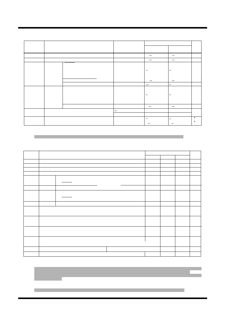
176
Tentative Specifications REV.A
Mitsubishi microcomputers
M16C / 62T Group
SINGLE-CHIP 16-BIT CMOS MICROCOMPUTER
S
pecifications in this manual are tentative and subject to change.
Under
development
Electrical characteristics
Table 1.26.1. Absolute maximum ratings
Note 1: When writing to EPROM ,only CNVss is 0.3 to 13.5 (V) .
Note 2: In case of 85
°
C guaranteed version, -40
°
C to 85
°
C. In case of 125
°
C guaranteed version, -40
°
C to 125
°
C.
Note 3: In M30623(80-pin package), P1
0
to P1
7
, P4
4
to P4
7
,P7
2
to P7
5
,and P9
1
are not connected to the external pin.
4.2
(Note 1)
5.5
Vcc
5.0
Vcc
AVcc
V
V
0
0
V
IH
I
OH (avg)
mA
mA
Vss
AVss
0.8Vcc
V
V
V
V
Vcc
0.2Vcc
0.2Vcc
0
0
I
OH (peak)
P7
0
to P7
7
, P8
0
to P8
7
, P9
0
to P9
7
, P10
0
to P10
7
,
-5
-10
P0
0
to P0
7
, P1
0
to P1
7
(during single-chip mode)
P0
0
to P0
7
, P1
0
to P1
7
,
P2
0
to P2
7
,P3
0
to P3
7
,
P4
0
to P4
7
, P5
0
to P5
7
,
P6
0
to P6
7
,P7
2
to P7
7
,
P8
0
to P8
4,
P8
6,
P8
7,
P9
0
to P9
7,
P10
0
to P10
7
(Note 4)
P2
0
to P2
7
, P3
0
to P3
7
, P4
0
to P4
7
, P5
0
to P5
7,
P6
0
to P6
7
,
10
5
mA
f
(X
IN
)
MHz
I
OL (peak)
mA
I
OL (avg)
16
f
(Xc
IN
)
kHz
50
32.768
V
X
IN
, RESET, CNV
SS
, BYTE
P0
0
to P0
7
, P2
0
to P2
7
,P3
0
to P3
7
,
P4
0
to P4
7
, P5
0
to P5
7
,
P6
0
to P6
7
,P7
2
to P7
7
,
P8
0
to P8
4,
P8
6,
P8
7,
P9
0
to P9
7,
P10
0
to P10
7
P0
0
to P0
7
, P2
0
to P2
7
,P3
0
to P3
7
,
P4
0
to P4
7
, P5
0
to P5
7
,
P6
0
to P6
7
,P7
0
to P7
7
,
P8
0
to P8
4,
P8
6,
P8
7,
P9
0
to P9
7,
P10
0
to P10
7
(Note 4)
P0
0
to P0
7
, P2
0
to P2
7
,P3
0
to P3
7
,
P4
0
to P4
7
, P5
0
to P5
7
,
P6
0
to P6
7
,P7
0
to P7
7
,
P8
0
to P8
4,
P8
6,
P8
7,
P9
0
to P9
7,
P10
0
to P10
7
Vcc=4.2V (Note 1) to 5.5V
0.8Vcc
V
V
IL
Symbol
Parameter
Unit
Standard
Min
Typ.
Max.
Supply voltage
Analog supply voltage
Supply voltage
Analog supply voltage
HIGH input
voltage
LOW input
voltage
HIGH peak output
current
HIGH average output
current
LOW peak output
current
LOW average
output current
Main clock input oscillation frequency
Subclock oscillation frequency
HIGH input voltage
V
IH
Vcc
P7
0
to P7
7
, P8
0
to P8
7
, P9
0
to P9
7
, P10
0
to P10
7
,
P2
0
to P2
7
, P3
0
to P3
7
, P4
0
to P4
7
, P5
0
to P5
7,
P6
0
to P6
7
,
X
IN
, RESET, CNV
SS
, BYTE
P0
0
to P0
7
, P1
0
to P1
7
(during single-chip mode)
LOW input voltage
V
IL
Table 1.26.2. Recommended operating conditions (referenced to V
CC
= 4.2V
(Note 1)
to 5.5V
at Ta = 40
o
C to 125
o
C
(Note 2)
unless otherwise specified)
Note 1: In case of One-time PROM version, 4.5V.
Note 2: In case of 85
°
C guaranteed version, -40
°
C to 85
°
C. In case of 125
°
C guaranteed version, -40
°
C to 125
°
C.
Note 3: The mean output current is the mean value within 100ms.
Note 4: In M30622(100-pin package), the total I
OL
(peak) and the total I
OH
(peak) for ports P0, P1, P2, P8
6
, P8
7
, P9, and P10 and the
total I
OL
(peak) and the total I
OH
(peak) for ports P3, P4, P5, P6, P7, and P8
0
to P8
4
severally must be 80mA max.
In M30623(80-pin package), Vcc pin and Vss pin are each one pin, so the total I
OL
(peak) and the total I
OH
(peak) for all ports
must be 80mA max.
Note 5: The loss power effect of the whole part-port(the output port transistor and the pull-up resistor) must be 50mW max,
so that power dissipation at Ta=125
°
C(include Ta >85
°
C) doesn't exceed absolute maximum ratings.
Note 6: In M30623(80-pin package), P1
0
to P1
7
, P4
4
to P4
7
,P7
2
to P7
5
, and P9
1
are not connected to the external pin.
X
OUT
V
O
P
d
40°C < Ta
85°C
V
V
V
V
I
AVcc
Vcc
T
stg
T
opr
mW
V
300
P3
0
to P3
7
, P4
0
to P4
3
, P5
0
to P5
7
,
P6
0
to P6
7
, P7
2
to P7
7
, P8
0
to P8
7
,
P0
0
to P0
7
, P1
0
to P1
7
, P2
0
to P2
7
,
P3
0
to P3
7
,P4
0
to P4
3
, P5
0
to P5
7
,
P6
0
to P6
7
,P7
2
to P7
7
, P8
0
to P8
4,
P0
0
to P0
7
, P1
0
to P1
7
, P2
0
to P2
7
,
RESET, V
REF
, X
IN
P9
0
to P9
7
, P10
0
to P10
7
P8
6
, P8
7
, P9
0
to P9
7
, P10
0
to P10
7
,
CNV
SS
, BYTE
P7
0
, P7
1
,
V
V
AV
CC
=V
CC,
AV
SS
=V
SS
C
C
Symbol
Parameter
Condition
Rated value
Unit
Supply voltage
Analog supply voltage
Input
voltage
Output
voltage
Power dissipation
Operating ambient temperature
Storage temperature
P7
0
, P7
1
V
AV
CC
=V
CC,
AV
SS
=V
SS
0.3 to 7
0.3 to 6.5
(Note 1)
200
300
200
85°C <Ta
125°C
0.3 to Vcc+0.3
40 to 125
(Note 2)
65 to 150
One-time PROM
version
Mask ROM
version
0.3 to 7
0.3 to 7
0.3 to 7
0.3 to 6.5
0.3 to 6.5
0.3 to 7
0.3 to 6.5
65 to 150
0.3 to Vcc+0.3
0.3 to Vcc+0.3
0.3 to Vcc+0.3
0.3 to Vcc+0.3
40 to 125
(Note 2)
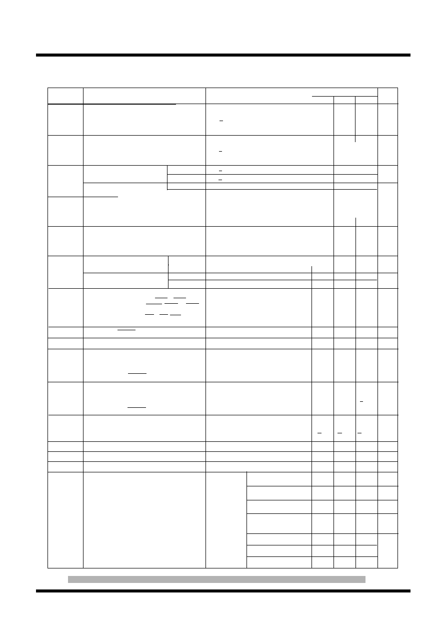
177
Tentative Specifications REV.A
Mitsubishi microcomputers
M16C / 62T Group
SINGLE-CHIP 16-BIT CMOS MICROCOMPUTER
S
pecifications in this manual are tentative and subject to change.
Under
development
Electrical characteristics
Table 1.26.3. Electrical characteristics (referenced to V
CC
= 5V, V
SS
= 0V at Ta = -40
o
C to 125
o
C
(Note 1)
,
f(X
IN
) = 16MH
Z
unless otherwise specified)
V
OH
V
OH
V
OH
V
OL
V
OL
V
OL
V
V
0.9Vcc
V
X
OUT
3.0
3.0
V
0.4Vcc
V
V
X
OUT
2.0
2.0
0.6Vcc
I
OL
=5mA
Vcc=4.0V to 5.5V
I
OL
=1mA
I
OL
=200µA
Vcc=4.0V to 5.5V
I
OL
=0.5mA
P0
0
to P0
7
, P1
0
to P1
7
, P2
0
to P2
7
,
P0
0
to P0
7
, P1
0
to P1
7
, P2
0
to P2
7
,
P3
0
to P3
7
, P4
0
to P4
7
, P5
0
to P5
7
,
P3
0
to P3
7
, P4
0
to P4
7
, P5
0
to P5
7
,
P6
0
to P6
7
, P7
2
to P7
7
, P8
0
to P8
4
,
P0
0
to P0
7
, P1
0
to P1
7
, P2
0
to P2
7
,
P3
0
to P3
7
, P4
0
to P4
7
, P5
0
to P5
7
,
P6
0
to P6
7
, P7
2
to P7
7
, P8
0
to P8
4
,
HIGHPOWER
LOWPOWER
P8
6
, P8
7
, P9
0
to P9
7
, P10
0
to P10
7
HIGHPOWER
LOWPOWER
P6
0
to P6
7
, P7
0
to P7
7
, P8
0
to P8
4
,
P8
6
, P8
7
, P9
0
to P9
7
, P10
0
to P10
7
P8
6
, P8
7
, P9
0
to P9
7
, P10
0
to P10
7
P0
0
to P0
7
, P1
0
to P1
7
, P2
0
to P2
7
,
P3
0
to P3
7
, P4
0
to P4
7
, P5
0
to P5
7
,
P6
0
to P6
7
, P7
0
to P7
7
, P8
0
to P8
4
,
P8
6
, P8
7
, P9
0
to P9
7
, P10
0
to P10
7
V
T+-
V
T-
0.2
0.8
V
Symbol
Parameter
Unit
Standard
Min
Typ.
Max.
HIGH output
voltage
HIGH output
voltage
HIGH output
voltage
LOW output
voltage
LOW output
voltage
LOW output
voltage
Hysteresis
I
IH
I
IL
V
RAM
Icc
V
T+-
V
T-
0.5
1.5
V
5
µA
2
V
2
µA
mA
RESET, CNVss, BYTE
50
P0
0
to P0
7
, P1
0
to P1
7
, P2
0
to P2
7
,
P3
0
to P3
7
, P4
0
to P4
7
, P5
0
to P5
7
,
P6
0
to P6
7
, P7
0
to P7
7
, P8
0
to P8
7
,
P9
0
to P9
7
, P10
0
to P10
7,
X
IN
, RESET, CNVss, BYTE
V
I
=5V
Pull-up resistance
V
I
=0V
28
38
f(X
IN
)=16MHz, Square wave,
P0
0
to P0
7
, P1
0
to P1
7
, P2
0
to P2
7
,
P3
0
to P3
7
, P4
0
to P4
7
, P5
0
to P5
7
,
P6
0
to P6
7
, P7
0
to P7
7
, P8
0
to P8
7
,
P9
0
to P9
7
, P10
0
to P10
7,
X
IN
, RESET, CNVss, BYTE
4.0
µA
f(X
IN
)=16kHz, Square wave,
24
P0
0
to P0
7
, P1
0
to P1
7
, P2
0
to P2
7
,
P3
0
to P3
7
, P4
0
to P4
7
, P5
0
to P5
7
,
P6
0
to P6
7
, P7
2
to P7
7
, P8
0
to P8
4
,
P8
6
, P8
7
, P9
0
to P9
7
, P10
0
to P10
7
No pull-up resistance
V
I
=0V
Hysteresis
HIGH input
current
LOW input
current
RAM retention voltage
Power supply current
µA
When clock is stopped
In single-chip
mode, the
output pins are
open and other
pins are Vss
diveide-by-1, no-wait
f(X
CIN
)=32kHz
Ta=125
°
C
when clock is stopped
Ta=25
°
C
when clock is stopped
Measuring condition
TA0
IN
to TA4
IN
, TA0
OUT
to TA4
OUT,
TB0
IN
to TB5
IN
, INT
0
to INT
5
,
P8
2
to P8
4
, AD
TRG
, CTS
0
to CTS
2
,
CLK
0
to CLK4, RXD
0
to RXD
2,
SIN
3
, SIN
4,
KI
0
to KI
3,
NMI
When a WAIT instruction is
executed, Ta=25
°
C
I
OH
=
5mA
Vcc=4.0V to 5.5V
I
OH
= 200µA
Vcc=4.0V to 5.5V
I
OH
= 0.5mA
I
OH
= 1mA
0.1Vcc
V
T+-
V
T-
X
IN
Hysteresis
0.2
0.8
V
I
IL
LOW input
current
µA
70
100
150
diveide-by-1, 1-wait
f(X
IN
)=16kHz, Square wave,
6.7
diveide-by-8, no-wait
mA
mA
5
X
COUT
HIGHPOWER
LOWPOWER
HIGH output
voltage
With no load applied
With no load applied
3.0
1.6
V
X
COUT
LOW output
voltage
HIGHPOWER
LOWPOWER
With no load applied
With no load applied
0
0
V
R
fXIN
R
fXCIN
Feedback resistance
X
IN
X
CIN
Feedback resistance
1.0
6.0
20
Ta=85
°
C
when clock is stopped
M
M
Note 1: In case of 85
°
C guaranteed version, -40
°
C to 85
°
C. In case of 125
°
C guaranteed version, -40
°
C to 125
°
C.
Note 2: In M30623(80-pin package), P1
0
to P1
7
, P4
4
to P4
7
,P7
2
to P7
5
, and P9
1
are not connected to the external pin.
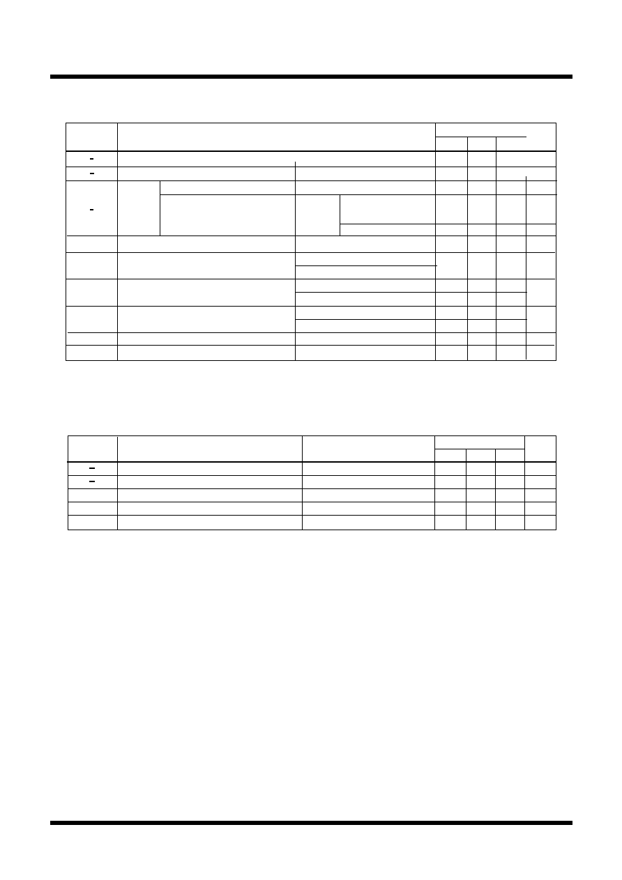
178
Tentative Specifications REV.A
Mitsubishi microcomputers
M16C / 62T Group
SINGLE-CHIP 16-BIT CMOS MICROCOMPUTER
S
pecifications in this manual are tentative and subject to change.
Under
development
Electrical characteristics
Table 1.26.4. A-D conversion characteristics (referenced to V
CC
= AV
CC
= 5V, Vss = AV
SS
= 0V, Ta = 25
o
C,
f(X
IN
) = 16MH
Z
unless otherwise specified)
µs
Standard
Min.
Typ. Max.
Resolution
Absolute
accuracy
Bits
LSB
V
REF
=
V
CC
= 5
V
±3
10
Symbol
Parameter
Measuring condition
Unit
V
REF
=
AV
CC
=
V
CC
= 5
V
,
AD
10MHz
R
LADDER
t
CONV
Ladder resistance
Conversion time
(10bit)
Reference voltage
Analog input voltage
k
V
V
IA
V
REF
V
0
2
10
V
CC
V
REF
40
Conversion time
(8bit)
3.3
t
CONV
t
SAMP
Sampling time
3.5
V
REF
=
V
CC
= 5V
Sample & hold function not available
Sample & hold function available
AN
0
to AN
7,
AN
00
to AN
07,
AN
20
to AN
27,
ANEX
0
, ANEX
1
input
External op-amp connection mode
V
REF
=AV
CC
=V
CC
=5V
AD
10MHz
LSB
LSB
±7
µs
µs
±3
Min.
Typ.
Max.
t
su
R
O
Resolution
Absolute accuracy
Setup time
Output resistance
Reference power supply input current
Bits
%
k
mA
I
VREF
1.0
1.5
8
3
Symbol
Parameter
Measuring condition
Unit
20
10
4
µs
(
Note 1
)
Standard
Note 1: Divide the frequency if f(X
IN
) exceeds 10 MHz, and make
AD
equal to or lower than 10 MHz.
(10bit)
f(X
IN
)=16MHz,
AD
= f
AD
/2 = 8MHz
4.125
f(X
IN
)=10MHz,
AD
= f
AD
= 10MHz
0.375
0.3
f(X
IN
)=16MHz,
AD
= f
AD
/2 = 8MHz
f(X
IN
)=10MHz,
AD
=
AD
= 10MHz
f(X
IN
)=16MHz,
AD
= f
AD
/2 = 8MHz
f(X
IN
)=10MHz,
AD
= f
AD
= 10MHz
2.8
Absolute accuracy(8bit)
V
REF
=
AV
CC
=
V
CC
= 5
V
,
AD
10MHz
LSB
±2
Table 1.26.5. D-A conversion characteristics (referenced to V
CC
= 5V, V
SS
= AV
SS =
0V, V
REF
= 5V
at Ta = 25
o
C, f(X
IN
) = 16MH
Z
unless otherwise specified)
Note 1: This applies when using one D-A converter, with the D-A register for the unused D-A converter set to
"00
16
". The A-D converter's ladder resistance is not included.
Note 2: When the Vref is unconnected at the A-D control register, I
VREF
is sent. When not using D-A
converter, with the D-A register for the unused D-A converter set to "00
16
", so that prevent dissipation
of unnecessary reference power supply current.
179
Tentative Specifications REV.A
Mitsubishi microcomputers
M16C / 62T Group
SINGLE-CHIP 16-BIT CMOS MICROCOMPUTER
S
pecifications in this manual are tentative and subject to change.
Under
development
Electrical characteristics
Max.
External clock rise time
ns
t
r
Min.
External clock input cycle time
External clock input HIGH pulse width
External clock input LOW pulse width
External clock fall time
ns
ns
ns
ns
t
c
t
w(H
)
t
w(L)
t
f
Parameter
Symbol
Unit
Standard
15
62.5
25
25
15
Standard
Max.
ns
TAi
IN
input LOW pulse width
t
w(TAL)
Min.
ns
ns
Unit
TAi
IN
input HIGH pulse width
t
w(TAH)
Parameter
Symbol
t
c(TA)
TAi
IN
input cycle time
60
150
60
Standard
Max.
Min.
ns
ns
ns
Unit
TAi
IN
input cycle time
TAi
IN
input HIGH pulse width
TAi
IN
input LOW pulse width
t
c(TA)
t
w(TAH)
t
w(TAL)
Symbol
Parameter
400
200
200
Standard
Max.
Min.
ns
ns
ns
Unit
TAi
IN
input cycle time
TAi
IN
input HIGH pulse width
TAi
IN
input LOW pulse width
t
c(TA)
t
w(TAH)
t
w(TAL)
Symbol
Parameter
200
100
100
Standard
Max.
Min.
ns
ns
Unit
t
w(TAH)
t
w(TAL)
Symbol
Parameter
TAi
IN
input HIGH pulse width
TAi
IN
input LOW pulse width
100
100
Standard
Max.
Min.
ns
ns
ns
Unit
ns
ns
Symbol
Parameter
TAi
OUT
input cycle time
TAi
OUT
input HIGH pulse width
TAi
OUT
input LOW pulse width
TAi
OUT
input setup time
TAi
OUT
input hold time
t
c(UP)
t
w(UPH)
t
w(UPL)
t
su(UP-T
IN
)
t
h(T
IN-
UP)
2000
1000
1000
400
400
Standard
Max.
Min.
ns
ns
t
w(INH)
t
w(INL)
Symbol
Parameter
Unit
INTi input LOW pulse width
INTi input HIGH pulse width
250
250
Timing requirements
Referenced to V
CC
= 5V, V
SS
= 0V at Ta = -40
o
C to 85
o
C (85
o
C guaranteed version), or Ta = -40
o
C to 125
o
C
(125
o
C guaranteed version) unless otherwise specified.
Table 1.26.9. Timer A input (gating input in timer mode)
Table 1.26.10. Timer A input (external trigger input in one-shot timer mode)
Table 1.26.11. Timer A input (external trigger input in pulse width modulation mode)
Table 1.26.12. Timer A input (up/down input in event counter mode)
Table 1.26.8. Timer A input (counter input in event counter mode)
_______
Table 1.26.7. External interrupt INTi inputs
Table 1.26.6. External clock input
180
Tentative Specifications REV.A
Mitsubishi microcomputers
M16C / 62T Group
SINGLE-CHIP 16-BIT CMOS MICROCOMPUTER
S
pecifications in this manual are tentative and subject to change.
Under
development
Electrical characteristics
Timing requirements
Referenced to V
CC
= 5V, V
SS
= 0V at Ta = - 40
o
C to 85
o
C(85
o
C guaranteed version), or Ta = - 40
o
C to
125
o
C(125
o
C guaranteed version) unless otherwise specified.
Standard
Max.
Min.
TBi
IN
input cycle time (counted on one edge)
TBi
IN
input HIGH pulse width (counted on one edge)
TBi
IN
input LOW pulse width (counted on one edge)
ns
ns
ns
t
c(TB)
t
w(TBH)
t
w(TBL)
Parameter
Symbol
Unit
t
c(TB)
t
w(TBL)
t
w(TBH)
ns
ns
ns
TBi
IN
input HIGH pulse width (counted on both edges)
TBi
IN
input LOW pulse width (counted on both edges)
TBi
IN
input cycle time (counted on both edges)
150
60
60
120
120
300
Standard
Max.
Min.
ns
ns
t
c(TB)
t
w(TBH)
Symbol
Parameter
Unit
t
w(TBL)
ns
TBi
IN
input HIGH pulse width
TBi
IN
input cycle time
TBi
IN
input LOW pulse width
400
200
200
Standard
Max.
Min.
ns
ns
t
c(TB)
Symbol
Parameter
Unit
t
w(TBL)
ns
t
w(TBH)
TBi
IN
input cycle time
TBi
IN
input HIGH pulse width
TBi
IN
input LOW pulse width
400
200
200
Standard
Max.
Min.
ns
ns
t
c(AD)
t
w(ADL)
Symbol
Parameter
Unit
AD
TRG
input cycle time (trigger able minimum)
AD
TRG
input LOW pulse width
1000
125
ns
ns
ns
ns
ns
ns
ns
Standard
Max.
Min.
CLKi input cycle time
CLKi input HIGH pulse width
CLKi input LOW pulse width
t
c(CK)
t
w(CKH)
t
w(CKL)
Parameter
Symbol
Unit
t
d(C-Q)
t
su(D-C)
t
h(C-Q)
TxDi / S
OUT
i hold time
RxDi / S
IN
i input setup time
TxDi / S
OUT
i output delay time
t
h(C-D)
RxDi / S
IN
i input hold time
250
125
125
0
45
120
100
When external clock is selected
When external clock is selected
ns
120
When external clock is selected
ns
45
When external clock is selected
Table 1.26.14. Timer B input (pulse period measurement mode)
Table 1.26.15. Timer B input (pulse width measurement mode)
Table 1.26.13. Timer B input (counter input in event counter mode)
Table 1.26.17. A-D trigger input
Table 1.26.16. Serial I/O
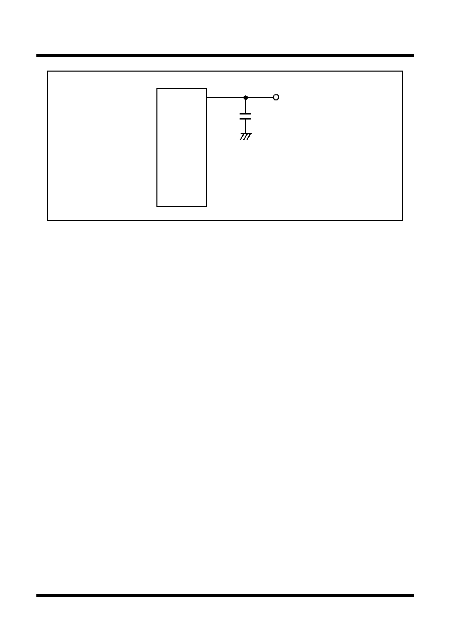
181
Tentative Specifications REV.A
Mitsubishi microcomputers
M16C / 62T Group
SINGLE-CHIP 16-BIT CMOS MICROCOMPUTER
S
pecifications in this manual are tentative and subject to change.
Under
development
Electrical characteristics
Figure 1.26.1. Port P0 to P10 measurement circuit
P6
P7
P8
P10
P9
P0
P1
P2
P3
P4
P5
30pF
Timing
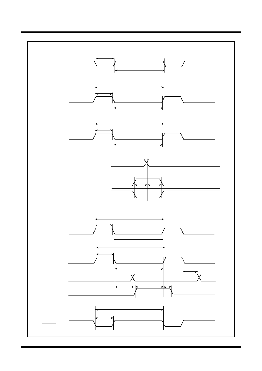
182
Tentative Specifications REV.A
Mitsubishi microcomputers
M16C / 62T Group
SINGLE-CHIP 16-BIT CMOS MICROCOMPUTER
S
pecifications in this manual are tentative and subject to change.
Under
development
Electrical characteristics
TAi
IN
input
t
c(TA)
t
w(TAH)
t
w(TAL)
TAi
OUT
input
t
c(UP)
t
w(UPH)
t
w(UPL)
TBi
IN
input
t
c(TB)
t
w(TBH)
t
w(TBL)
t
w(INL)
t
w(INH)
INTi input
t
c(AD)
t
w(ADL)
AD
TRG
input
During event counter mode
t
h(T
IN
UP)
t
su(UPT
IN
)
TAi
IN
input
(When count on falling
edge is selected)
TAi
IN
input
(When count on rising
edge is selected)
TAi
OUT
input
(Up/down input)
t
su(DC)
CLKi
TxDi / S
OUT
i
RxDi / S
IN
i
t
c(CK)
t
w(CKH)
t
w(CKL)
t
d(CQ)
t
h(CD)
t
h(CQ)
Vcc=5V
Figure 1.26.2. Timing
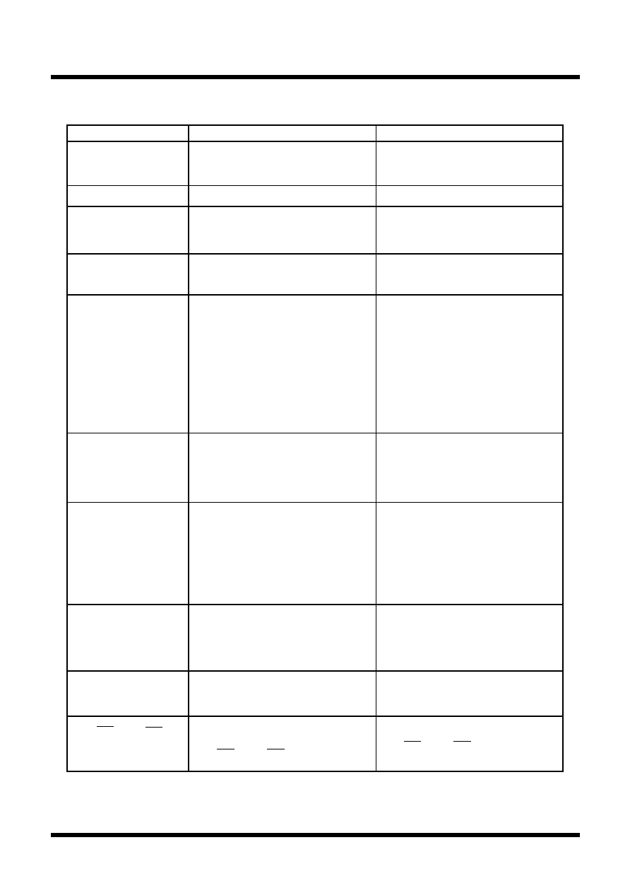
183
Tentative Specifications REV.A
Mitsubishi microcomputers
M16C / 62T Group
SINGLE-CHIP 16-BIT CMOS MICROCOMPUTER
S
pecifications in this manual are tentative and subject to change.
Under
development
Differences between M16C/62T group and M16C/61T group
Group
M16C/62T group
M16C/61T group
Serial I/O
UART/clocked SI/O · · · · · 3 channel
(80-pin package: One of exclusive UART)
Clocked SI/O · · · · · · · · · · 2 channel
(80-pin package: One of exclusive transmission)
UART/clocked SI/O · · · · · 3 channels
(80-pin package: One of exclusive UART)
Port function
P9
0
· · · · · TB0
IN
/CLK3
P9
1
· · · · · TB1
IN
/S
IN
3
P9
2
· · · · · TB2
IN
/S
OUT
3
P9
3
· · · · · TB3
IN
/DA0
P9
4
· · · · · TB4
IN
/DA1
P9
5
· · · · · ANEX0/CLK4
P9
6
· · · · · ANEX1/S
OUT
4
P9
7
· · · · · AD
TRG
/S
IN
4
P1
5
· · · · · D13/INT3
P1
6
· · · · · D14/INT4
P1
7
· · · · · D15/INT5
P7
1
· · · · · R
X
D
2
/TA0
IN
/TB5
IN
P9
0
· · · · · TB0
IN
P9
1
· · · · · TB1
IN
P9
2
· · · · · TB2
IN
P9
3
· · · · · DA0
P9
4
· · · · · DA1
P9
5
· · · · · ANEX0
P9
6
· · · · · ANEX1
P9
7
· · · · · AD
TRG
P1
5
· · · · · D13
P1
6
· · · · · D14
P1
7
· · · · · D15
P7
1
· · · · · R
X
D
2
/TA0
IN
Interrupt cause
Internal 20 sources
External 5 sources
Software 4 sources
Internal 25 sources, External 8 sources
(80-pin package: 5 sources),
Software 4 sources
(Added 2 Serial I/O, 3 timers and
3external interrupts
(Note 2)
)
Three-phase inverter
control circuit
PWM output for three-phase inverter
can be performed using timer A4, A1
and A2.
Output port is arranged to P7
2
to P7
5
,
P8
0
and P8
1
.
Impossible
IIC bus mode
UART2 used
IIC bus interface can be performed
with software
Impossible
Memory space (Note 1)
Memory expansion is possible
1.2M bytes mode
4M bytes mode
1M byte fixed
Timer B
6 channels
3 channels
Chip select
CS0 : 30000
16
to FFFFF
16
CS1 : 28000
16
to 2FFFF
16
CS2 : 08000
16
to 27FFF
16
CS3 : 04000
16
to 07FFF
16
M16C/61T type (wrinting the right) and
the type as below can be switched
(Besides 4M-byte mode is possible.)
CS0 : 04000
16
to 3FFFF
16
(fetch)
40000
16
to FFFFF
16
(data/facth)
CS1 : 28000
16
to 2FFFF
16
(data)
CS2 : 08000
16
to 27FFF
16
(data)
CS3 : 04000
16
to 07FFF
16
(data)
Read port P1
By setting to register, the state of port
register can be read always.
The state of port when input mode.
The state of port register when output
mode.
P4
4
/CS0 - P4
7
/CS3
If a Vcc level is applied to the CNVss
pin, bit 2 (PU11) of pull-up control
register 1 turns to "1" when reset, and
P4
4
/
CS0
- P4
7
/
CS3
turn involved in
pull-up.
Bit 2 (PU11) of the pull-up control
register 1 turns to "0" when reset, and
P4
4
/
CS0
- P4
7
/
CS3
turn free from pull-
up.
(Note 2)
(Note 2)
(Note 2)
(Note 2)
(Note 2)
(Note 2)
(Note 1) (Note 2)
(Note 2)
(Note 2)
(Note 1) (Note 2)
Note 1: M16C/61T group, and M16C/62T group are not guaranteed operating of memory expansion, but it is
mentioned in the table for clear the difference of capacity.
Note 2: In 80-pin package(M30613, M30623), pins of a part are not connected to the external pin, so do not
use these functions and pins.

MITSUBISHI SEMICONDUCTORS
M16C/62T Group Tentative Specification REV.A
Jan First Edition 1999
Editioned by
Committee of editing of Mitsubishi Semiconductor
Published by
Mitsubishi Electric Corp., Kitaitami Works
This book, or parts thereof, may not be reproduced in any form without
permission of Mitsubishi Electric Corporation.
©1999 MITSUBISHI ELECTRIC CORPORATION