1. DESCRIPTION
The M306V2ME-XXXFP and M306V2EEFP are single-chip microcomputers using the high-performance
silicon gate CMOS process using a M16C/60 Series CPU core and are packaged in a 100-pin plastic
molded QFP. These single-chip microcomputers operate using sophisticated instructions featuring a high
level of instruction efficiency. With 1M bytes of address space, they are capable of executing instructions at
high speed. They also feature a built-in OSD display function and data slicer, making them ideal for control-
ling TV with a closed caption decoder.
The features of the M306V2EEFP are similar to those of the M306V2ME-XXXFP except that this chip has
a built-in PROM which can be written electrically.
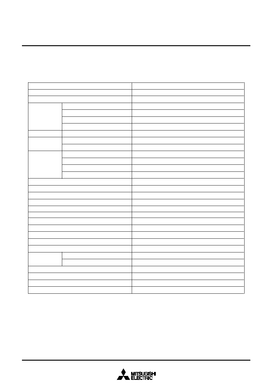
1.1 Features
· Memory size ........................................ <ROM>192K bytes
<RAM> 5K bytes
<OSD ROM> 61K bytes
<OSD RAM> 2.2K bytes
· Shortest instruction execution time ...... 100 ns (f(X
IN
)=10 MHz)
· Power sourse voltage .......................... 4.5 V to 5.5V
· Power consumption ............................. 250 mW
· Interrupts .............................................. 21 internal and 3 external interrupt sources, 4 software
interrupt sources; 7 levels
· Multifunction 16-bit timer ...................... 2 output timers + 3 input timers + 3 timers
· Serial I/O .............................................. 3 units
UART/clock synchronous: 2
Multi-master I
2
C-BUS interface 0 (2 systems): 1
Multi-master I
2
C-BUS interface 1 (1 system): 1
· DMAC .................................................. 2 channels (trigger: 23 sources)
· A-D converter ....................................... 8 bits
!
6 channels
· D-A converter ....................................... 8 bits
!
2 channels
· Data slicer ............................................ 1 circuit
· H
SYNC
counter ..................................... 1 circuit (2 systems)
· OSD function ....................................... 1 circuit
· Watchdog timer .................................... 1 circuit
· Programmable I/O ............................... 78 lines
· Memory expansion .............................. Available
· Chip select output ................................ 4 lines
· Clock generating circuit ....................... 3 built-in clock generation circuits
1.2 Applications
TV with a closed caption decoder
MITSUBISHI MICROCOMPUTERS
M306V2ME-XXXFP
M306V2EEFP
SINGLE-CHIP 16-BIT CMOS MICROCOMPUTER with CLOSED CAPTION DECODER
and ON-SCREEN DISPLAY CONTROLLER
1
Rev. 1.0

M306V2ME-XXXFP
M306V2EEFP
MITSUBISHI MICROCOMPUTERS
SINGLE-CHIP 16-BIT CMOS MICROCOMPUTER with CLOSED CAPTION DECODER
and ON-SCREEN DISPLAY CONTROLLER
2
Rev. 1.0
------Table of Contents------
2.16.18 Scan Mode ................................ 230
2.16.19 R, G, B Signal Output Control ... 230
2.16.20 OSD Reserved Register ........... 231
2.17 Programmable I/O Ports .................... 232
3. USAGE PRECAUTION .............................. 245
3.1 Timer A (timer mode) ........................... 245
3.2 Timer A (event counter mode) ............. 245
3.3 Timer A (one-shot timer mode) ............ 245
3.4 Timer A (pulse width modulation mode) .... 245
3.5 Timer B (timer mode, event counter mode) ..... 246
3.6 Timer B (pulse period/pulse width
measurement mode) ........................... 246
3.7 A-D Converter ...................................... 246
3.8 Stop Mode and Wait Mode .................. 246
3.9 Interrupts .............................................. 247
3.10 Built-in PROM version ....................... 248
4. ITEM TO BE SUBMITTED WHEN ORDERING
MASKED ROM VERSION ......................... 249
5. ELECTRICAL CHARACTERISTICS .......... 250
5.1 Absolute Maximum Ratings ................. 250
5.2 Recommended Operating Conditions .. 251
5.3 Electrical Characteristics ..................... 252
5.4 A-D Conversion Characteristics ........... 253
5.5 D-A Conversion Characteristics ........... 253
5.6 Analog R, G, B Output Characteristics 253
5.7 Timing Requirements ........................... 254
5.8 Switching Characteristics ..................... 255
5.9 Measurement Circuit ............................ 259
5.10 Timing Diagram ................................. 260
6. MASK ROM CONFIRMATION FORM ....... 265
7. MARK SPECIFICATION FORM ................ 269
8.ONE TIME PROM VERSION
M306V2EEFP MARKING ........................... 270
9. PACKAGE OUTLINE ................................. 271
1. DESCRIPTION .............................................. 1
1.1 Features ................................................... 1
1.2 Applications ............................................. 1
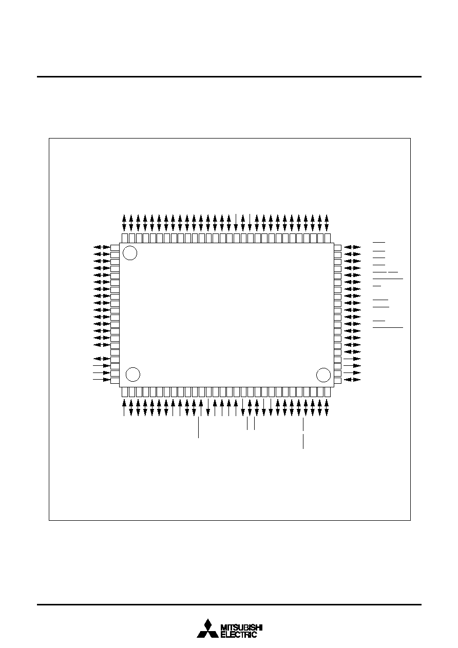
1.3 Pin Configuration ..................................... 3
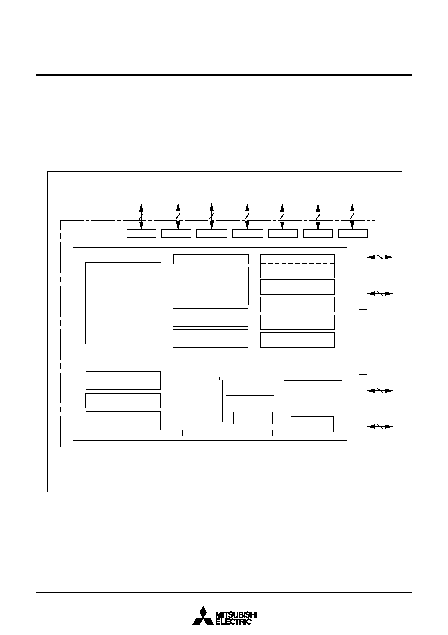
1.4 Block Diagram ......................................... 4
1.5 Performance Outline ................................ 5
2. OPERATION OF FUNCTIONAL BLOCKS .... 9
2.1 Memory .................................................... 9
2.2 Central Processing Unit (CPU) .............. 15
2.3 Reset ..................................................... 18
2.4 Processor Mode ..................................... 23
2.5 Clock Generating Circuit ........................ 36
2.6 Protection ............................................... 46
2.7 Interrupts ................................................ 47
2.8 Watchdog Timer .................................... 67
2.9 DMAC .................................................... 69
2.10 Timer .................................................... 79
2.11 Serial I/O .............................................. 99
2.12 A-D Converter .................................... 149
2.13 D-A Converter .................................... 164
2.14 Data Slicer ......................................... 166
2.15 H
SYNC
Counter .................................. 176
2.16 OSD Function .................................... 177
2.16.1 Triple Layer OSD ........................ 183
2.16.2 Display Position .......................... 185
2.16.3 Dot Size ...................................... 189
2.16.4 Clock for OSD ............................. 190
2.16.5 Field Determination Display ........ 191
2.16.6 Memory for OSD ......................... 193
2.16.7 Character Color .......................... 206
2.16.8 Character Background Color ...... 206
2.16.9 OUT1, OUT2 Signals .................. 211
2.16.10 Attribute .................................... 212
2.16.11 Automatic Solid Space Function ..... 217
2.16.12 Particular OSD Mode Block ...... 218
2.16.13 Multiline Display ........................ 220
2.16.14 SPRITE OSD Function ............. 221
2.16.15 Window Function ...................... 224
2.16.16 Blank Function .......................... 225
2.16.17 Raster Coloring Function .......... 228
M306V2ME-XXXFP
M306V2EEFP
MITSUBISHI MICROCOMPUTERS
SINGLE-CHIP 16-BIT CMOS MICROCOMPUTER with CLOSED CAPTION DECODER
and ON-SCREEN DISPLAY CONTROLLER
5
Rev. 1.0
Item
Performance
Number of basic instructions
91 instructions
Shortest instruction execution time
100 ns(f(X
IN
)=10 MHz)
Memory
ROM
192K bytes
size
RAM
5K bytes
OSD ROM
61K bytes
OSD RAM
2.2K bytes
I/O port
P0 to P10
8 bits
!
8, 5 bits
!
2, 4 bits
!
1
Multifunction
TA0, TA1, TA2, TA3, TA4
16 bits
!
5
timer
TB0, TB1, TB2
16 bits
!
3
Serial I/O
UART0
1 unit: UART or clock synchronous
UART2
1 unit: UART or clock synchronous
Multi-master I
2
C-BUS interface 0 1 unit (2 channels)
Multi-master I
2
C-BUS interface 1 1 unit (1 channel)
A-D converter
8 bits
!
6 channels
D-A converter
8 bits
!
2 channels
DMAC
2 channels (trigger: 23 sources)
OSD function
Triple layer, 890 kinds of fonts, 42 character
!
16 lines
Data slicer
32-bit buffer
H
SYNC
counter
8 bits
!
2 channels
Watchdog timer
15 bits
!
1 (with prescaler)
Interrupt
21 internal and 3 external sources, 4 software sources, 7 levels
Clock generating circuit
3 built-in clock generation circuits
Power source voltage
4.5 V to 5.5V (f(X
IN
) = 10 MHz)
Power consumption
250 mW
I/O
I/O withstand voltage
5 V
characteristics
Output current
5 mA
Memory expansion
Available
Operating ambient temperature
10
o
C to 70
o
C
Device configuration
CMOS high performance silicon gate
Package
100-pin plastic molded QFP
Table 1.5.1 Performance outline
1.5 Performance Outline
Table 1.5.1 is a performance outline.