1
Under
development
Preliminary Specifications REV.D
Specifications in this manual are tentative and subject to change.
Mitsubishi microcomputers
M16C/80 (100-pin version) group
SINGLE-CHIP 16-BIT CMOS MICROCOMPUTER
Description
------Table of Contents------
Description
The M16C/80 (100-pin version) group of single-chip microcomputers are built using the high-performance
silicon gate CMOS process using a M16C/60 Series CPU core and are packaged in a 100-pin plastic
molded QFP. These single-chip microcomputers operate using sophisticated instructions featuring a high
level of instruction efficiency. With 16M bytes of address space, they are capable of executing instructions
at high speed. They also feature a built-in multiplier and DMAC, making them ideal for controlling office,
communications, industrial equipment, and other high-speed processing applications.
The M16C/80 (100-pin version) group includes a wide range of products with different internal memory
types and sizes and various package types.
Features
· Memory capacity .................................. ROM (See ROM expansion figure.)
RAM 10/20 Kbytes
· Shortest instruction execution time ...... 50ns (f(X
IN
)=20MHz)
· Supply voltage ..................................... 4.0 to 5.5V (f(X
IN
)=20MHz) Mask ROM and flash memory version
2.7 to 5.5V (f(X
IN
)=10MHz) Mask ROM and flash memory version
· Low power consumption ...................... 45mA (M30800MC-XXXFP)
· Interrupts .............................................. 29 internal and 8 external interrupt sources, 5 software
interrupt sources; 7 levels (including key input interrupt)
· Multifunction 16-bit timer ...................... 5 output timers + 6 input timers
· Serial I/O .............................................. 5 channels for UART or clock synchronous
· DMAC .................................................. 4 channels (trigger: 31 sources)
· DRAMC ................................................ Used for EDO, FP, CAS before RAS refresh, self-refresh
· A-D converter ....................................... 10 bits X 8 channels (Expandable up to 10 channels)
· D-A converter ....................................... 8 bits X 2 channels
· CRC calculation circuit ......................... 1 circuit
· X-Y converter ....................................... 1 circuit
· Watchdog timer .................................... 1 line
· Programmable I/O ............................... 87 lines
· Input port ..............................................
_______
1 line (P8
5
shared with NMI pin)
· Memory expansion .............................. Available (16M bytes)
· Chip select output ................................ 4 lines
· Clock generating circuit ....................... 2 built-in clock generation circuits
(built-in feedback resistance, and external ceramic or quartz oscillator)
Applications
Audio, cameras, office equipment, communications equipment, portable equipment, etc.
A-D Converter ............................................. 162
D-A Converter ............................................. 172
CRC Calculation Circuit .............................. 174
X-Y converter .............................................. 176
DRAM controller .......................................... 179
Programmable I/O Ports ............................. 186
Usage Precaution ....................................... 201
Electric characteristics ................................ 208
Flash memory version ................................. 255
CPU .............................................................. 11
Reset ............................................................. 16
Processor Mode ............................................ 24
Clock Generating Circuit ............................... 40
Protection ...................................................... 52
Interrupts ....................................................... 53
Watchdog Timer ............................................ 75
DMAC ........................................................... 77
Timer ............................................................. 88
Serial I/O ..................................................... 120
Specifications written in this
manual are believed to be ac-
curate, but are not guaranteed
to be entirely free of error.
Specifications in this manual
may be changed for functional
or performance improvements.
Please make sure your manual
is the latest edition.
Under
development
Preliminary Specifications REV.D
Specifications in this manual are tentative and subject to change.
Mitsubishi microcomputers
M16C/80 (100-pin version) group
SINGLE-CHIP 16-BIT CMOS MICROCOMPUTER
4
Description
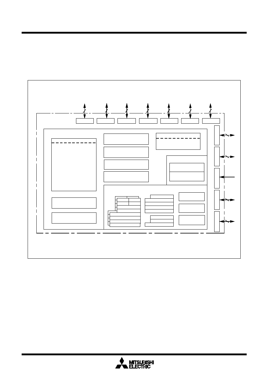
Block Diagram
Figure 1.1.3 is a block diagram of the M16C/80 (100-pin version) group.
Block diagram of the M30800MC-XXXGP
Figure 1.1.3. Block diagram of M30800MC-XXXFP
R0L
R0H
R1H
R1L
R2
I/O ports
8
8
8
8
8
8
8
8
7
8
8
Internal peripheral functions
Timer
Timer TA0 (16 bits)
Timer TA1 (16 bits)
Timer TA2 (16 bits)
Timer TA3 (16 bits)
Timer TA4 (16 bits)
Timer TB0 (16 bits)
Timer TB1 (16 bits)
Timer TB2 (16 bits)
Timer TB3 (16 bits)
Timer TB4 (16 bits)
Timer TB5 (16 bits)
Watchdog timer
(15 bits)
D-A converter
(8 bits X 2 channels)
A-D converter
(10 bits X 8 channels
Expandable up to 10 channels)
UART /clock synchronous SI/O
(8 bits X 5 channels)
X-Y converter
(16 bits X 16 bits)
CRC arithmetic circuit (CCITT)
(Polynomial : X +X +X +1)
System clock generator
X
IN
- X
OUT
X
CIN
- X
COUT
Memory
DRAM
controller
M16C/80 series 16-bit CPU core
Registers
R0H
R0L
R1H
R1L
R2
R3
A0
A1
FB
SB
DRAM
controller
Multiplier
Port P0
Port P1
Port P2
Port P3
Port P4
Port P5
Port P6
Port P7
Port P8
Port P8
5
Port P9
Port P10
FLG
INTB
ISP
USP
PC
SVF
SVP
VCT
12
16
5
ROM
(Note 1)
RAM
(Note 2)
Note 1: ROM size depends on MCU type.
Note 2: RAM size depends on MCU type.
5
Under
development
Preliminary Specifications REV.D
Specifications in this manual are tentative and subject to change.
Mitsubishi microcomputers
M16C/80 (100-pin version) group
SINGLE-CHIP 16-BIT CMOS MICROCOMPUTER
Description
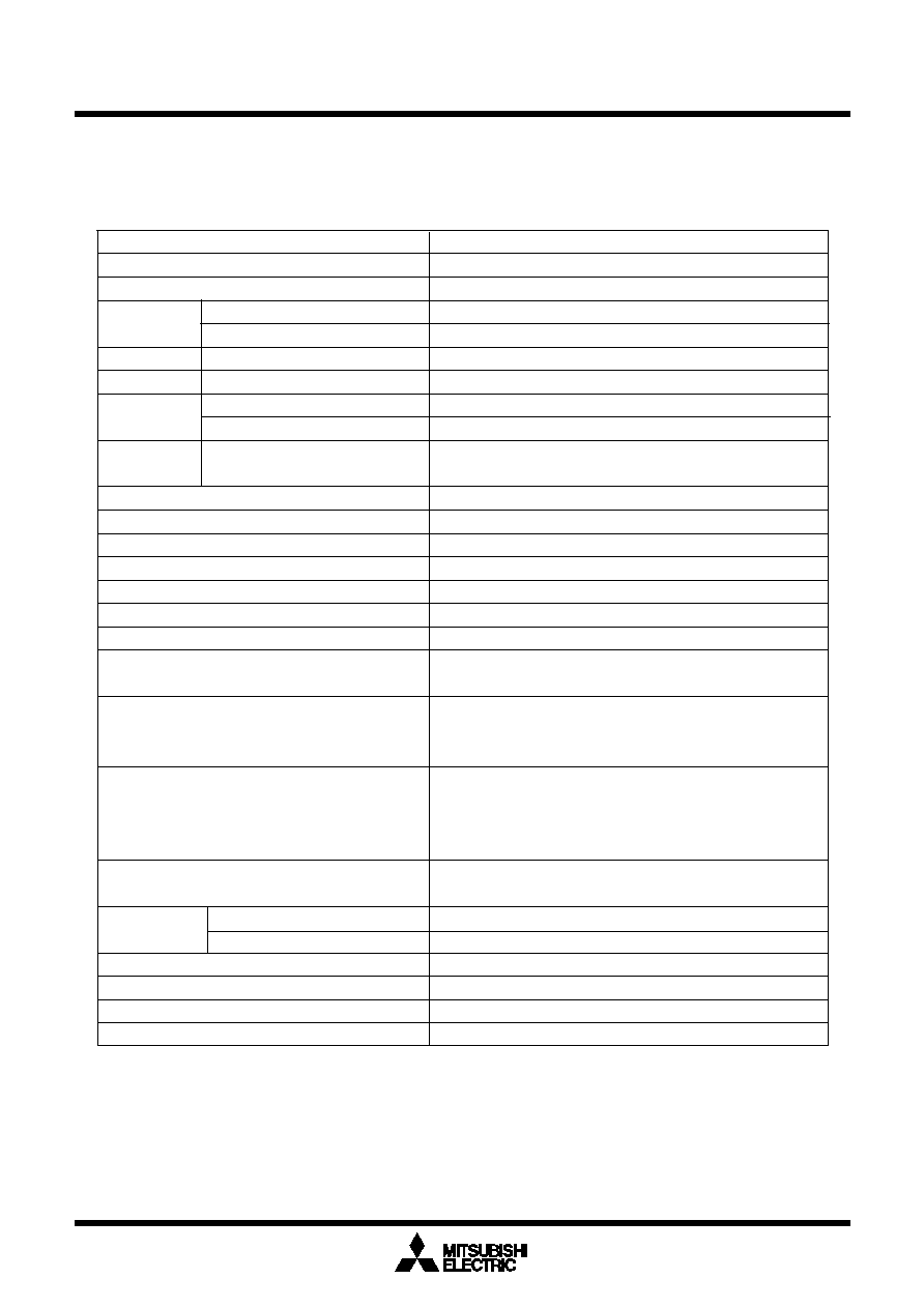
Item
Performance
Number of basic instructions
106 instructions
Shortest instruction execution time
50ns(f(X
IN
)=20MHz)
Memory
See ROM expansion figure.
capacity
10/20 K bytes
I/O port
8 bits x 10, 7 bits x 1
Input port
1 bit x 1
Multifunction
16 bits x 5
timer
16 bits x 6
Serial I/O
(UART or clock synchronous) x 5
A-D converter
10 bits x (8 + 2) channels
D-A converter
8 bits x 2
DMAC
4 channels
DRAM controller
CAS before RAS refresh, self-refresh, EDO, FP
CRC calculation circuit
CRC-CCITT
X-Y converter
16 bits X 16 bits
Watchdog timer
15 bits x 1 (with prescaler)
Interrupt
29 internal and 8 external sources, 5 software sources, 7
levels
Clock generating circuit
2 built-in clock generation circuits
(built-in feedback resistance, and external ceramic or
quartz oscillator)
Supply voltage
4.2 to 5.5V (f(X
IN
)=20MHz) Mask ROM and flash
memory version
2.7 to 5.5V (f(X
IN
)=10MHz) Mask ROM and flash
memory version
Power consumption
45mA (f(X
IN
) = 20MHz without software wait,Vcc=5V)
Mask ROM 128 Kbytes version
I/O
5V
characteristics
5mA
Memory expansion
Available (up to 16M bytes)
Operating ambient temperature
40 to 85
o
C
Device configuration
CMOS high performance silicon gate
Package
100-pin plastic mold QFP
Table 1.1.1. Performance outline of M16C/80 (100-pin version) group
Performance Outline
Table 1.1.1 is a performance outline of M16C/80 (100-pin version) group.
ROM
RAM
P0 to P10 (except P8
5
)
P8
5
TA0, TA1, TA2, TA3,TA4
TB0, TB1, TB2, TB3, TB4, TB5
UART0, UART1, UART2,
UART3, UART4
I/O withstand voltage
Output current