
MITSUBISHI
ELECTRIC
SINGLE-CHIP 4-BIT CMOS MICROCOMPUTER
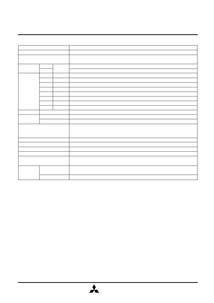
ROM type
Mask ROM
One Time PROM
Package
20P2N-A
20P2N-A
RAM size
(
!
4 bits)
64 words
64 words
*: Shipped after writing (shipped in blank: M34250E2FP)
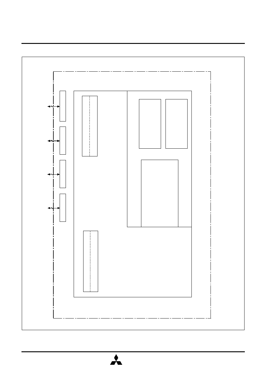
PIN CONFIGURATION (TOP VIEW)
M34250M2-XXXFP
ROM (PROM) size
(
!
9 bits)
2048 words
2048 words
Product
M34250M2-XXXFP
M34250E2-XXXFP *
V
D D
2
3
4
5
6
7
8
9
10
1
19
18
17
16
15
14
13
12
11
20
G
2
S
0
S
1
S
2
S
3
D
3
/K
D
2
/C
D
1
D
0
G
3
V
SS
G
1
/T
OUT
G
0
/INT
RESET
X
IN
X
OUT
CNV
SS
F
0
F
1
M34250M2-XXXF
P
Outline 20P2N-A
DESCRIPTION
The 4250 Group is a 4-bit single-chip microcomputer designed
with CMOS technology. Its CPU is that of the 720 series using a
simple instruction set. The computer is equipped with one 8-bit
timer which has a reload register and the interrupt function.
The various microcomputers in the 4250 Group include variations
of the built-in memory type as shown in the table below.
FEATURES
∑ Minimum instruction execution time ............................. 1.0
µ
s
(at 4.0 MHz system clock frequency, V
DD
=4.5 V to 5.5 V)
∑ Supply voltage
4.5 V to 5.5 V (at 4.0 MHz system clock frequency)
2.5 V to 5.5 V (at 1.0 MHz system clock frequency)
2.2 V to 5.5 V (at 1.0 MHz system clock frequency:
only for Mask ROM version)
∑ Timer
Timer 1 ................................ 8-bit timer with a reload register
∑ Interrupt ................................................................... 2 sources
∑ CR oscillation circuit (Capacitor and Resistor connected
externally)
∑ Logic operation instruction
∑ RAM back-up function
∑ Key-on wakeup function (ports G and S, INT pin)
APPLICATION
Electric household appliances, consumer electronics products
(mouse, etc.)
MITSUBISHI MICROCOMPUTERS
4250 Group
MITSUBISHI
ELECTRIC
2
MITSUBISHI MICROCOMPUTERS
4250 Group
SINGLE-CHIP 4-BIT CMOS MICROCOMPUTER
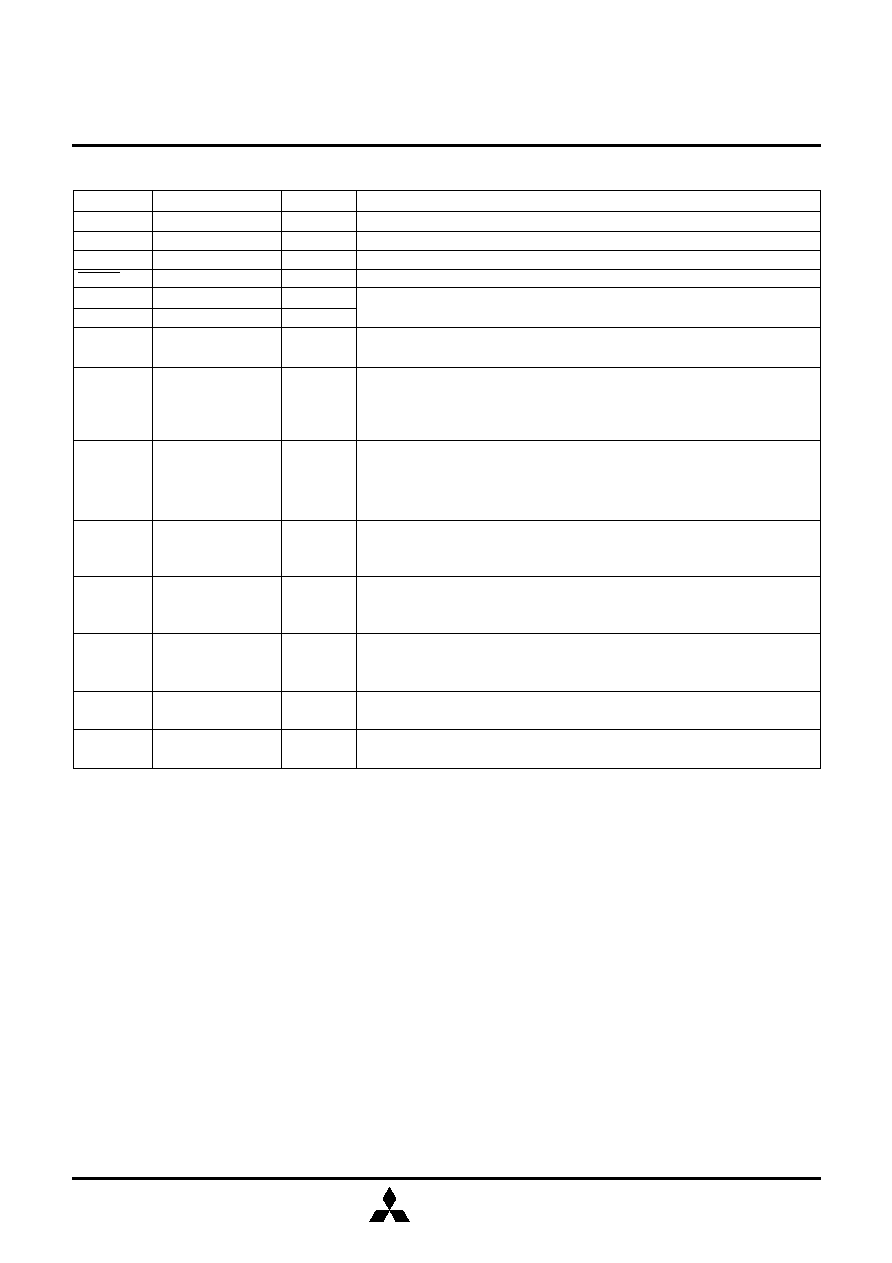
RAM
(64 words
!
4 bits)
ROM
(2048 words
!
9 bits)
720 series
CPU core
Memory
I/O port
Internal peripheral functions
Timer
Timer 1 (8 bits)
System clock generating circuit
X
IN
-X
OUT
(Note)
Note: PROM 2048 words
!
9 bits
Register B (4 bits)
Register A (4 bits)
Register D (3 bits)
Register E (8 bits)
Stack register (SK) (4 levels)
Interrupt stack register (SDP) (1 level)
ALU (4 bits)
Port D
4
Port S
4
Port G
4
Port F
2
BLOCK DIAGRAM
MITSUBISHI
ELECTRIC
3
MITSUBISHI MICROCOMPUTERS
4250 Group
SINGLE-CHIP 4-BIT CMOS MICROCOMPUTER
PERFORMANCE OVERVIEW
Function
70
1.0
µ
s (at 4.0 MHz system clock frequency) (Refer to the electrical characteristics because
the minimum instruction execution time depends on the supply voltage.)
2048 words
!
9 bits
64 words
!
4 bits
Four independent I/O ports; ports D
2
and D
3
are also used as ports C and K, respectively.
4-bit I/O port
1-bit I/O port; port C is also used as port D
2
.
1-bit I/O port; port K is also used as port D
3
.
2-bit I/O port
4-bit I/O port; ports G
0
and G
1
are also used as pins INT and T
OUT
.
Interrupt input; INT pin is also used as port G
0
.
Timer output; T
OUT
pin is also used as port G
1
.
8-bit timer with a reload register
2 (one for external and one for timer)
1 level
CR oscillation circuit (a capacitor and a resistor connected externally)
Frequency error:
±
17 %
(V
DD
= 5 V
±
10 %, V
DD
= 3 V
±
10 %, the error of the external capacitor and resistor excluded)
4 levels
CMOS silicon gate
20-pin plastic molded SOP (20P2N-A)
≠20
∞
C to 85
∞
C
2.2 V to 5.5 V (Refer to the electrical characteristics because the supply voltage depends on
the system clock frequency.)
1.5 mA
(at 4.0 MHz system clock frequency, V
DD
= 5 V, output transistors in the cut-off state)
0.1
µ
A (at room temperature, V
DD
= 5 V, output transistors in the cut-off state)
Parameter
Number of basic instructions
Minimum instruction execution time
Memory sizes
Input/Output
ports
Timer
Interrupt
Oscillation circuit
Subroutine nesting
Device structure
Package
Operating temperature range
Supply voltage
Power
dissipation
(typical value)
ROM
RAM
D
0
≠D
3
S
0
≠S
3
C
K
F
0
, F
1
G
0
≠G
3
INT
T
OUT
Timer 1
Sources
Nesting
Active mode
RAM back-up mode
M34250M2/
E2
I/O
I/O
I/O
I/O
I/O
I/O
Input
Output
MITSUBISHI
ELECTRIC
4
MITSUBISHI MICROCOMPUTERS
4250 Group
SINGLE-CHIP 4-BIT CMOS MICROCOMPUTER
PIN DESCRIPTION
Name
Power supply
Ground
CNV
SS
Reset input
System clock input
System clock output
I/O port F
I/O port G
I/O port S
I/O port D
I/O port C
I/O port K
Timer output
Interrupt input
Input/Output
--
--
--
Input
Input
Output
I/O
I/O
I/O
I/O
I/O
I/O
Output
Input
Function
Connected to a plus power supply.
Connected to a 0 V power supply.
Connect CNV
SS
to V
SS
and apply "L" (0V) to CNV
SS
certainly.
Reset pulse input pin
I/O pins of the system clock generating circuit. Connect pins X
IN
and X
OUT
directly.
Then, pull up X
IN
pin through a resistor and pull down X
OUT
pin through a capacitor.
2-bit I/O port; for input use, set the latch of the specified bit to "1." The output
structure is N-channel open-drain.
4-bit I/O port. For input use, set the latch of the specified bit to "1." The output
structure is N-channel open-drain. Every pin of the ports has a key-on wakeup
function and a pull-up function. Both functions can be switched by software.
Ports G
0
and G
1
are also used as pins INT and T
OUT
, respectively.
4-bit I/O port. For input use, set the latch of the specified bit to "1." The output
structure is N-channel open-drain. Every pin of the ports has a key-on wakeup
function which can be switched by software. Also, it is used to perform the logic
operation using register A.
Each pin of port D has an independent 1-bit wide I/O function. For input use, set
the latch of the specified bit to "1." The output structure is N-channel open-drain.
Ports D
2
and D
3
are also used as ports C and K, respectively.
1-bit I/O port. For input use, set the latch of the specified bit to "1." The output
structure is N-channel open-drain. Port C has a pull-up function which can be
switched by software. It is also used as port D
2
.
1-bit I/O port. For input use, set the latch of the specified bit to "1." The output
structure is N-channel open-drain. Port K has a pull-up function which can be
switched by software. It is also used as port D
3
.
T
OUT
pin has the function to output the timer 1 underflow signal divided by 2. It is
also used as port G
1
.
INT pin accepts an external interrupt. It also accepts the input signal to return the
system from the RAM back-up state. It is also used as port G
0
.
Pin
V
DD
V
SS
CNV
SS
RESET
X
IN
X
OUT
F
0
, F
1
G
0
≠G
3
S
0
≠S
3
D
0
≠D
3
C
K
T
OUT
INT
MITSUBISHI
ELECTRIC
5
MITSUBISHI MICROCOMPUTERS
4250 Group
SINGLE-CHIP 4-BIT CMOS MICROCOMPUTER
MULTIFUNCTION
Pin
G
0
G
1
D
2
D
3
Multifunction
INT
T
OUT
C
K
Multifunction
G
0
G
1
D
2
D
3
Pin
INT (Note 2)
T
OUT
(Note 2)
C (Note 2)
K (Note 2)
Notes 1: Pins except above have just single function.
2: The I/O of ports D
2
, D
3
and G
0
, and the input of port G
1
can be used even when ports C and K and pins INT and T
OUT
are
selected.
CONNECTIONS OF UNUSED PINS
Pin
F
0
, F
1
G
0
/INT, G
1
/T
OUT
G
2
, G
3
S
0
≠S
3
Connection
Connect to V
SS
pin.
Open or connect to V
SS
pin. (Note 3)
Pin
D
0
, D
1
D
2
/C, D
3
/K
Connection
Connect to V
SS
pin.
Open or connect to V
SS
pin. (Note 1)
Connect to V
SS
pin. (Note 2)
Notes 1: When pins G
0
/INT, G
1
/T
OUT
, G
2
and G
3
are connected to V
SS
pin, turn off their pull-up transistors (Pull-up control register
PU0="
!
0
2
") and also invalidate the key-on wakeup functions of pins G
1
/T
OUT
, G
2
and G
3
(Key-on wakeup contorl register
K0="
!!
0
!
2
") by software. When the POF instruction is executed while these pins are connected to V
SS
and the key-on
wakeup functions are left valid, the system returns from RAM back-up state by recognizing the return condition immediately
after going into the RAM back-up state. When these pins are open, turn on their pull-up transistors (Pull-up control register
PU0="
!
1
2
") by software.
2: When ports S
0
≠S
3
are connected to V
SS
pin, invalidate the key-on wakeup functions (Key-on wakeup contorl register
K0="
!!!
0
2
") by software. When the POF instruction is executed while these pins are connected to V
SS
and the key-on
wakeup functions are left valid, the system returns from RAM back-up state by recognizing the return condition immediately
after going into the RAM back-up state.
3: When ports D
2
/C and D
3
/K are connected to V
SS
pin, turn off their pull-up transistors (register PU0="0
!
2
") by software.
When these pins are open, turn on their pull-up transistors (register PU0="1
!
2
") by software.
(Note when connecting to V
SS
and V
DD
)
∑ Connect the unused pins to V
SS
or V
DD
at the shortest distance and use the thick wire against noise.