Document Outline
- ˛ˇ
- ˛ˇ
- ˛ˇ
- ˛ˇ
- ˛ˇ
- ˛ˇ
- ˛ˇ
- ˛ˇ
- ˛ˇ
- ˛ˇ
- ˛ˇ
- ˛ˇ
- ˛ˇ
- ˛ˇ
- ˛ˇ
- ˛ˇ
- ˛ˇ
- ˛ˇ
- ROM ORDERING METHOD
- ˛ˇ
- ˛ˇ
- ˛ˇ
- ˛ˇ
- ˛ˇ
- ˛ˇ
- ˛ˇ
- ˛ˇ
- ˛ˇ
- ˛ˇ
- ˛ˇ
ROM type
Mask ROM
Mask ROM
One Time PROM
Package
20P2E/F-A
20P2E/F-A
20P2E/F-A
RAM size
(
◊
4 bits)
48 words
64 words
64 words
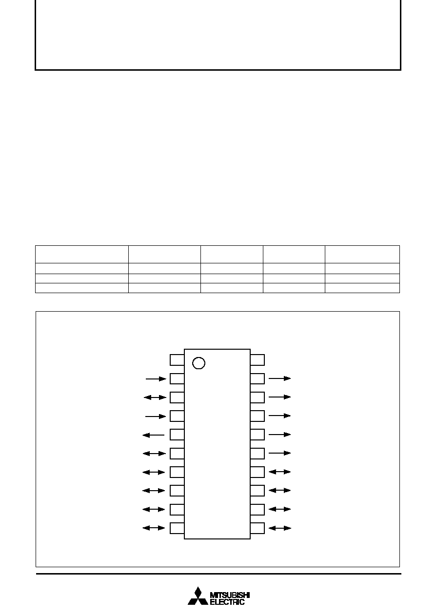
PIN CONFIGURATION (TOP VIEW)
ROM (PROM) size
(
◊
9 bits)
1024 words
2048 words
2048 words
Product
M34282M1-XXXGP *
M34282M2-XXXGP *
M34282E2GP *
DESCRIPTION
The 4282 Group enables fabrication of 8
◊
7 key matrix and has
the followin timers;
∑ an 8-bit timer which can be used to set each carrier wave and
has two reload register
∑ an 8-bit timer which can be used to auto-control and has a
reload register.
FEATURES
∑ Number of basic instructions ............................................. 68
∑ Minimum instruction execution time ............................ 8.0
µ
s
(at f(X
IN
) = 4.0 MHz, system clock = f(X
IN
)/8)
∑ Supply voltage ................................................. 1.8 V to 3.6 V
∑ Subroutine nesting ..................................................... 4 levels
∑ Timer
Timer 1 ................................................................... 8-bit timer
(This has a reload register and carrier wave output auto-control
function)
Timer 2 ................................................................... 8-bit timer
(This has two reload registers and carrier wave output function)
∑ Logic operation function (XOR, OR, AND)
∑ RAM back-up function
∑ Key-on wakeup function (ports D
4
≠D
7
, E
0
≠E
2
, G
0
≠G
3
) .... 11
∑ I/O port (ports D, E, G, CARR) .......................................... 16
∑ Oscillation circuit ..................................... Ceramic resonance
∑ Watchdog timer
∑ Power-on reset circuit
∑ Voltage drop detection circuit ......................... Typical:1.50 V
(system reset)
APPLICATION
Various remote control transmitters
4282 Group
SINGLE-CHIP 4-BIT CMOS MICROCOMPUTER
MITSUBISHI MICROCOMPUTERS
V
S
S
2
3
4
5
6
7
8
9
10
1
1
9
18
17
1
6
15
1
4
1
3
1
2
1
1
20
D
7
D
2
D
3
D
4
D
5
D
1
D
0
CARR
V
DD
D
6
E
2
G
3
G
2
E
0
E
1
X
IN
X
O
U
T
G
0
G
1
M
3
4
2
8
2
M
x
-
X
X
X
G
P
PRELIMINAR
Y
Notice: This is not a final specification.
Some parametric limits are subject to change.
* : Under development (June, 2000)
Outline 20P2E/F-A
MITSUBISHI
ELECTRIC
2
MITSUBISHI MICROCOMPUTERS
4282 Group
SINGLE-CHIP 4-BIT CMOS MICROCOMPUTER
PRELIMINAR
Y
Notice: This is not a final specification.
Some parametric limits are subject to change.
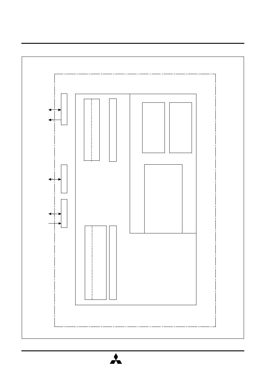
BLOCK DIAGRAM
R
A
M
(
4
8
,
6
4
w
o
r
d
s
4
b
i
t
s
)
R
O
M
(
1
0
2
4
,
2
0
4
8
w
o
r
d
s
9
b
i
t
s
)
7
2
0
s
e
r
i
e
s
C
P
U
c
o
r
e
M
e
m
o
r
y
I
/
O
p
o
r
t
I
n
t
e
r
n
a
l
p
e
r
i
p
h
e
r
a
l
f
u
n
c
t
i
o
n
T
i
m
e
r
/
R
e
m
o
t
e
-
c
o
n
t
r
o
l
c
a
r
r
i
e
r
-
w
a
v
e
o
u
t
p
u
t
T
i
m
e
r
1
(
8
b
i
t
s
,
c
a
r
r
i
e
r
w
a
v
e
o
u
t
p
u
t
c
o
n
t
r
o
l
)
T
i
m
e
r
2
(
8
b
i
t
s
,
c
a
r
r
i
e
r
w
a
v
e
g
e
n
e
r
a
t
i
o
n
)
S
y
s
t
e
m
c
l
o
c
k
g
e
n
e
r
a
t
i
o
n
c
i
r
c
u
i
t
X
I
N
-
X
O
U
T
(
N
o
t
e
)
R
e
g
i
s
t
e
r
B
(
4
b
i
t
s
)
R
e
g
i
s
t
e
r
A
(
4
b
i
t
s
)
R
e
g
i
s
t
e
r
D
(
3
b
i
t
s
)
R
e
g
i
s
t
e
r
E
(
8
b
i
t
s
)
S
t
a
c
k
r
e
g
i
s
t
e
r
S
K
(
4
l
e
v
e
l
s
)
A
L
U
(
4
b
i
t
s
)
P
o
r
t
D
4
P
o
r
t
G
4
P
o
r
t
E
2
4
1
W
a
t
c
h
d
o
g
t
i
m
e
r
(
1
4
b
i
t
s
)
R
e
s
e
t
(
v
o
l
t
a
g
e
d
r
o
p
d
e
t
e
c
t
i
o
n
c
i
r
c
u
i
t
)
N
o
t
e
:
P
R
O
M
2
0
4
8
w
o
r
d
s
9
b
i
t
s
,
R
A
M
6
4
w
o
r
d
s
4
b
i
t
s
f
o
r
b
u
i
l
t
-
i
n
P
R
O
M
v
e
r
s
i
o
n
.

MITSUBISHI
ELECTRIC
3
MITSUBISHI MICROCOMPUTERS
4282 Group
SINGLE-CHIP 4-BIT CMOS MICROCOMPUTER
PRELIMINAR
Y
Notice: This is not a final specification.
Some parametric limits are subject to change.
PERFORMANCE OVERVIEW
Function
68
8.0
µ
s (f(X
IN
) = 4.0 MHz, system clock = f(X
IN
)/8, V
DD
= 3 V)
2048 words
9 bits
1024 words
9 bits
64 words
4 bits
48 words
4 bits
Four independent output ports
Four independent I/O ports with the pull-down function
3-bit input port with the pull-down function
2-bit output port (E
0
, E
1
)
4-bit I/O port with the pull-down function
1-bit output port; CMOS output
8-bit timer with a reload register
8-bit timer with two reload registers
4 levels (However, only 3 levels can be used when the TABP p instruction is executed)
CMOS silicon gate
20-pin plastic molded SSOP (20P2E/F-A)
≠20 ∞C to 85 ∞C
1.8 V to 3.6 V
400
µ
A
(f(X
IN
) = 4.0 MHz, system clock = f(X
IN
)/8, V
DD
= 3 V)
0.1
µ
A (at room temperature, V
DD
= 3 V)
Parameter
Number of basic instructions
Minimum instruction execution time
Memory sizes
Input/Output
ports
Timer
Subroutine nesting
Device structure
Package
Operating temperature range
Supply voltage
Power
dissipation
(typical value)
ROM
RAM
D
0
≠D
3
D
4
≠D
7
E
0
≠E
2
E
0
, E
1
G
0
≠G
3
CARR
Timer 1
Timer 2
Active mode
RAM back-up mode
M34282M2/E2
M34282M1
M34282M2/E2
M34282M1
Output
I/O
Input
Output
I/O
Output
PIN DESCRIPTION
Name
Power supply
Ground
System clock input
System clock output
Output port D
I/O port D
I/O port E
I/O port G
Carrier wave output
for remote control
Input/Output
--
--
Input
Output
Output
I/O
Output
Input
I/O
Output
Function
Connected to a plus power supply.
Connected to a 0 V power supply.
I/O pins of the system clock generating circuit. Connect a ceramic resonator
between pins X
IN
and X
OUT
. The feedback resistor is built-in between pins X
IN
and X
OUT
.
Each pin of port D has an independent 1-bit wide output function. The output
structure is P-channel open-drain.
1-bit I/O port. For input use, set the latch of the specified bit to "0." When the built-
in pull-down transistor is turned on, the key-on wakeup function using "H" level
sense and the pull-down transistor become valid. The output structure is P-channel
open-drain.
2-bit (E
0
, E
1
) output port. The output structure is P-channel open-drain.
3-bit input port. For input use (E
0
, E
1
), set the latch of the specified bit to "0."
When the built-in pull-down transistor is turned on, the key-on wakeup function
using "H" level sense and the pull-down transistor become valid. Port E
2
has an
input-only port and has a key-on wakeup function using "H" level sense and pull-
down transistor.
4-bit I/O port. For input use, set the latch of the specified bit to "0." The output structure
is P-channel open-drain. When the built-in pull-down transistor is turned on, the key-
on wakeup function using "H" level sense and pull-down transistor become valid.
Carrier wave output pin for remote control. The output structure is CMOS circuit.
Pin
V
DD
V
SS
X
IN
X
OUT
D
0
≠D
3
D
4
≠D
7
E
0
≠E
2
G
0
≠G
3
CARR
MITSUBISHI
ELECTRIC
4
MITSUBISHI MICROCOMPUTERS
4282 Group
SINGLE-CHIP 4-BIT CMOS MICROCOMPUTER
PRELIMINAR
Y
Notice: This is not a final specification.
Some parametric limits are subject to change.
CONNECTIONS OF UNUSED PINS
Pin
D
0
≠D
7
E
0
, E
1
E
2
G
0
≠G
3
Connection
Open or connect to V
DD
pin (Note 1).
Set the output latch to "1" and open, or
connect to V
DD
pin (Note 2).
Open or connect to V
SS
pin.
Set the output latch to "1" and open, or
connect to V
DD
pin (Note 2).
Notes 1: Ports D
4
≠D
7
: Set the bit 2 (PU0
2
) of the pull-down control register PU1 to "0" by software and turn the pull-down transistor
OFF.
2: Set the corresponding bits of the pull-down control register PU0 to "0" by software and turn the pull-down transistor OFF.
(Note in order to set the output latch to "1" to make pins open)
∑ After system is released from reset, a port is in a high-impedance state until the output latch of the port is set to "1" by software.
Accordingly, the voltage level of pins is undefined and the excess of the supply current may occur.
∑ To set the output latch periodically is recommended because the value of output latch may change by noise or a program run away
(caused by noise).
(Note when connecting to V
SS
and V
DD
)
∑ Connect the unused pins to V
SS
or V
DD
at the shortest distance and use the thick wire against noise.
PORT FUNCTION
Control
bits
1 bit
Output:
2 bits
Input:
3 bits
4 bits
1 bit
Control
instructions
SD
RD
CLD
SD
RD
CLD
SZD
OEA
IAE
IAE
OGA
IAG
SCAR
RCAR
Control
registers
PU1
PU0
PU0
Output structure
P-channel open-drain
P-channel open-drain
P-channel open-drain
CMOS
Input/
Output
Output
(4)
I/O
(4)
I/O
(2)
Input
(1)
I/O
(4)
Output
(1)
Remark
Pull-down function and
key-on wakeup function
(programmable)
Pull-down function and
key-on wakeup function
(programmable)
Pull-down function and
key-on wakeup function
(programmable)
Pin
D
0
≠D
3
D
4
≠D
7
E
0
E
1
E
2
G
0
≠G
3
CARR
Port
Port D
Port E
Port G
Port CARR
DEFINITION OF CLOCK AND CYCLE
∑ System clock (STCK)
The system clock is the source clock for controlling this product.
It can be selected as shown below whether to use the CCK
instruction.
CCK instruction
When not using
When using
Instruction clock
f(X
IN
)/32
f(X
IN
)/4
System clock
f(X
IN
)/8
f(X
IN
)
∑ Instruction clock (INSTCK)
The instruction clock is a signal derived by dividing the system
clock by 4, and is the basic clock for controlling CPU. The one
instruction clock cycle is equivalent to one machine cycle.
∑ Machine cycle
The machine cycle is the cycle required to execute the
instruction.
MITSUBISHI
ELECTRIC
5
MITSUBISHI MICROCOMPUTERS
4282 Group
SINGLE-CHIP 4-BIT CMOS MICROCOMPUTER
PRELIMINAR
Y
Notice: This is not a final specification.
Some parametric limits are subject to change.
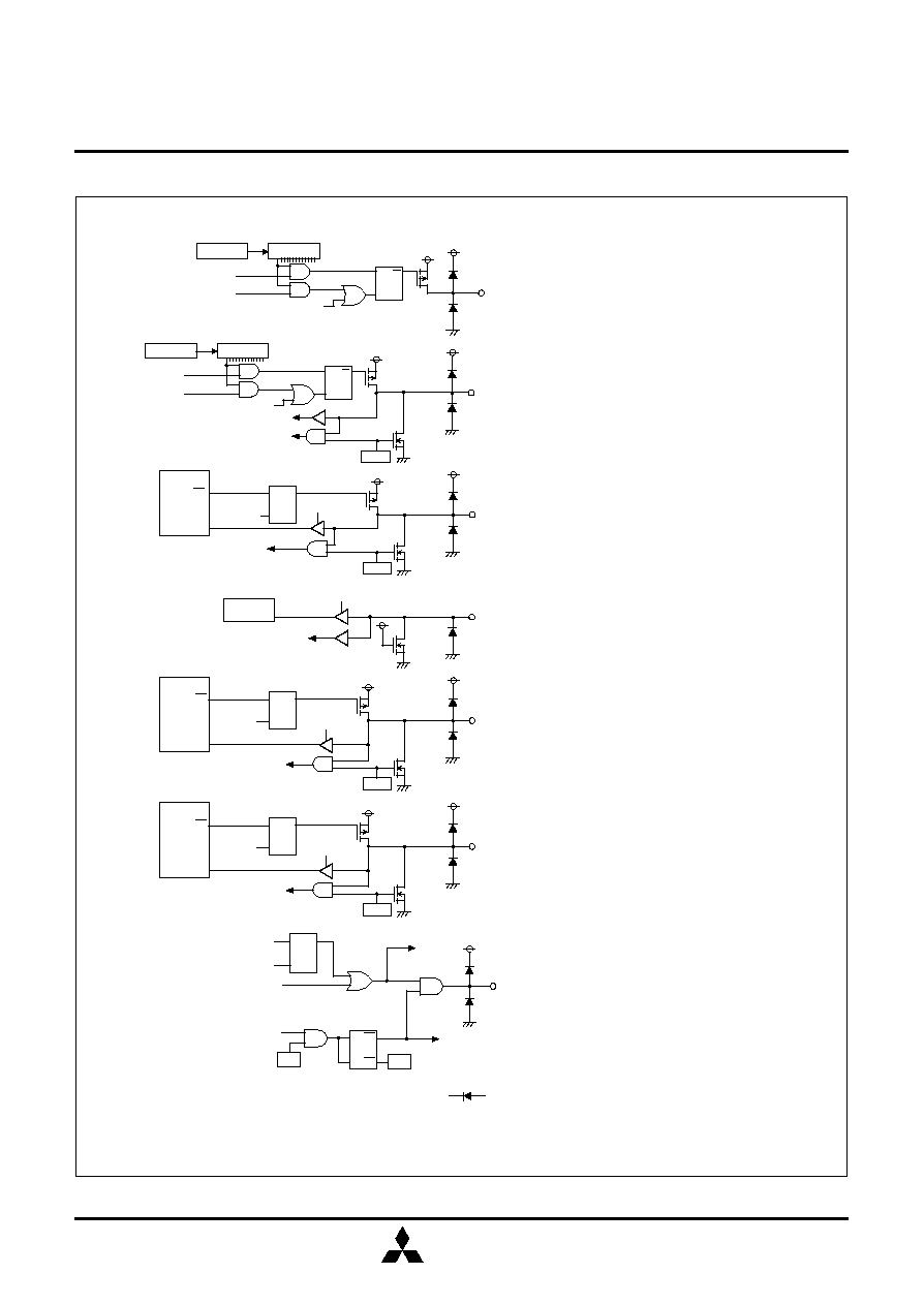
PORT BLOCK DIAGRAMS
CLD instruction
SD instruction
RD instruction
Ports D
0
≠D
3
S
R
Q
Decoder
Register Y
(Note 1)
Port E
2
(Note 5)
Key-on wakeup input
IAE instruction
Register A
A
2
Skip decision (SZD instruction)
CLD instruction
SD instruction
RD instruction
S
R
Q
Decoder
Register Y
PU1
i
Pull-down transistor
Key-on wakeup
(Note 2)
Ports E
0
, E
1
(Note 5)
OEA
instruction
Register A
A
j
A
j
D
T
Q
PU0
j
Key-on wakeup input
IAE instruction
(Note 3)
(Note 3)
Ports G
0
, G
1
(Note 5)
Key-on wakeup input
OGA
instruction
IAG instruction
Register A
A
j
A
j
D
T
Q
(Note 3)
PU0
2
Port CARR
(Note 1)
Timer 1 underflow signal
D
T
Q
R
V1
0
Carrier wave output control signal
CARRY
(to timer 1)
V1
2
CARRYD
(from timer 2)
S
R
Q
SCAR instruction
RCAR instruction
CAR flag
PU0
3
Key-on wakeup input
OGA
instruction
IAG instruction
Register A
A
k
A
k
D
T
Q
(Note 1)
(Note 4)
(Note 1)
Ports D
4
≠D
7
(Note 5)
Pull-down
transistor
(Note 1)
(Note 1)
(Note 1)
Pull-down
transistor
Pull-down transistor
Pull-down transistor
Ports G
2
, G
3
(Note 5)
Notes 1:
2: i represents bits 0 to 3.
3: j represents bits 0, 1.
4: k represents bits 2, 3.
5: Applied voltage must be less than VDD.
This symbol represents a parasitic diode.