DESCRIPTION
The 4513/4514 Group is a 4-bit single-chip microcomputer de-
signed with CMOS technology. Its CPU is that of the 4500 series
using a simple, high-speed instruction set. The computer is
equipped with serial I/O, four 8-bit timers (each timer has a reload
register), and 10-bit A-D converter.
The various microcomputers in the 4513/4514 Group include varia-
tions of the built-in memory type and package as shown in the
table below.
FEATURES
q
Minimum instruction execution time ................................ 0.75
µ
s
(at 4.0 MHz oscillation frequency, in high-speed mode, V
DD
= 4.0
V to 5.5 V)
q
Supply voltage
∑ Middle-speed mode
...... 2.5 V to 5.5 V (at 4.2 MHz oscillation frequency, for Mask
ROM version and One Time PROM version)
...... 2.0 V to 5.5 V (at 3.0 MHz oscillation frequency, for Mask
ROM version)
(Operation voltage of A-D conversion: 2.7 V to 5.5 V)
∑ High-speed mode
...... 4.0 V to 5.5 V (at 4.2 MHz oscillation frequency, for Mask
ROM version and One Time PROM version)
...... 2.5 V to 5.5 V (at 2.0 MHz oscillation frequency, for Mask
ROM version and One Time PROM version)
...... 2.0 V to 5.5 V (at 1.5 MHz oscillation frequency, for Mask
ROM version)
(Operation voltage of A-D conversion: 2.7 V to 5.5 V)
q
Timers
Timer 1 ...................................... 8-bit timer with a reload register
Timer 2 ...................................... 8-bit timer with a reload register
Timer 3 ...................................... 8-bit timer with a reload register
Timer 4 ...................................... 8-bit timer with a reload register
q
Interrupt ........................................................................ 8 sources
q
Serial I/O ....................................................................... 8 bit-wide
q
A-D converter .................. 10-bit successive comparison method
q
Voltage comparator ........................................................ 2 circuits
q
Watchdog timer ................................................................. 16 bits
q
Voltage drop detection circuit
q
Clock generating circuit (ceramic resonator)
q
LED drive directly enabled (port D)
APPLICATION
Microwave oven, rice cooker, audio, telephone, office equipment
Note: shipped in blank
* : Under development
**: Under planning
Product
M34513M2-XXXSP/FP *
M34513M4-XXXSP/FP *
M34513E4SP/FP * (Note)
M34513M6-XXXFP **
M34513M8-XXXFP **
M34513E8FP ** (Note)
M34514M6-XXXFP *
M34514M8-XXXFP *
M34514E8FP * (Note)
ROM type
Mask ROM
Mask ROM
One Time PROM
Mask ROM
Mask ROM
One Time PROM
Mask ROM
Mask ROM
One Time PROM
Package
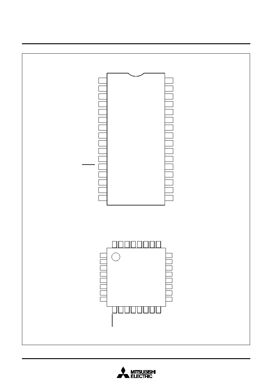
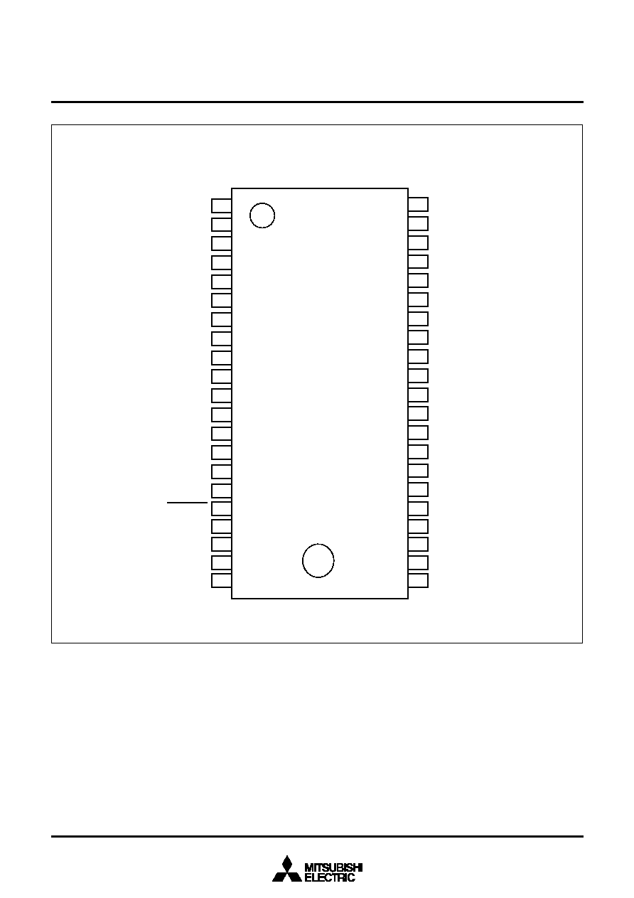
SP: 32P4B FP: 32P6B-A
SP: 32P4B FP: 32P6B-A
SP: 32P4B FP: 32P6B-A
32P6B-A
32P6B-A
32P6B-A
42P2R-A
42P2R-A
42P2R-A
RAM size
(
!
4 bits)
128 words
256 words
256 words
384 words
384 words
384 words
384 words
384 words
384 words
ROM (PROM) size
(
!
10 bits)
2048 words
4096 words
4096 words
6144 words
8192 words
8192 words
6144 words
8192 words
8192 words
4513/4514 Group
SINGLE-CHIP 4-BIT CMOS MICROCOMPUTER
MITSUBISHI MICROCOMPUTERS
PRELIMINAR
Y
Notice: This is not a final specification.
Some parametric limits are subject to
change.
4
4513/4514 Group
SINGLE-CHIP 4-BIT CMOS MICROCOMPUTER
MITSUBISHI MICROCOMPUTERS
PRELIMINAR
Y
Notice: This is not a final specification.
Some parametric limits are subject to
change.
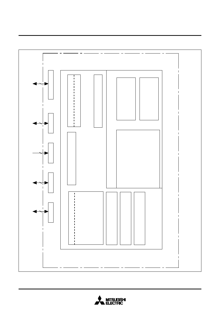
BLOCK DIAGRAM (4513 Group)
|[go
1
Voltage drop detection circuit
4
Serial
I/O
(8
b
i
ts
!
1)
Voltage comparator
(2 circuits)
X
IN
≠X
OUT
I/O port
Internal peripheral functions
Timer
System clock generating circuit
Watchdog timer
(16 bits)
Memory
ROM
2048, 4096,6144, 8192
words
◊
10 bits
RAM
128, 256, 384 words
◊
4 bits
4500 Series
CPU core
ALU (4 bits)
Register A (4 bits) Register B (4 bits)
Register D (3 bits) Register E (8 bits)
Stack register SK (8 levels)
Interrupt stack register SDP (1 level)
Timer 1 (8 bits)
Timer 2 (8 bits)
Timer 3 (8 bits)
Timer 4 (8 bits)
A-D converter
(10 bits
!
4 ch)
Port D
Port P3
Port P2
Port P1
Port P0
4
3
2
8
5
4513/4514 Group
SINGLE-CHIP 4-BIT CMOS MICROCOMPUTER
MITSUBISHI MICROCOMPUTERS
PRELIMINAR
Y
Notice: This is not a final specification.
Some parametric limits are subject to
change.
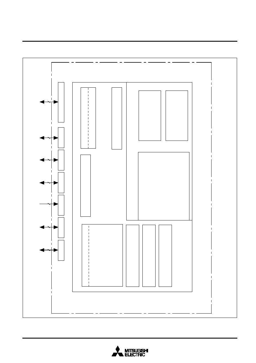
BLOCK DIAGRAM (4514 Group)
Voltage drop detection circuit
S
e
r
i
a
l
I/O
(8
b
i
ts
!
1)
Voltage comparator
(2 circuits)
X
IN
--X
OUT
I/O port
Internal peripheral functions
Timer
System clock generating circuit
Watchdog timer
(16 bits)
Memory
ROM
6144, 8192 words
◊
10 bits
RAM
384 words
◊
4 bits
4500 Series
CPU core
ALU (4 bits)
Register A (4 bits) Register B (4 bits)
Register D (3 bits) Register E (8 bits)
Stack register SK (8 levels)
Interrupt stack register SDP (1 level)
Timer 1 (8 bits)
Timer 2 (8 bits)
Timer 3 (8 bits)
Timer 4 (8 bits)
A-D converter
(10 bits
!
8 ch)
Port D
Port P3
Port P2
Port P1
Port P0
Port P5
Port P4
4
4
4
4
4
8
3