Document Outline
- DESCRIPTION
- FEATURES
- APPLICATION
- PIN CONFIGURATION (TOP VIEW)
- BLOCK DIAGRAM
- PERFORMANCE OVERVIEW
- DEFINITION OF CLOCK AND CYCLE
- PIN DESCRIPTION
- MULTIFUNCTION
- CONNECTIONS OF UNUSED PINS
- PORT FUNCTION
- PORT BLOCK DIAGRAMS
- FUNCTION BLOCK OPERATIONS
- PROGRAM MEMORY (ROM)
- DATA MEMORY (RAM)
- INTERRUPT FUNCTION
- EXTERNAL INTERRUPTS
- TIMERS
- WATCHDOG TIMER
- CARRIER WAVE GENERATING CIRCUIT
- RESET FUNCTION
- VOLTAGE DROP DETECTION CIRCUIT
- RAM BACK-UP MODE
- CLOCK CONTROL
- ROM ORDERING METHOD
- LIST OF PRECAUTIONS
- SYMBOL
- LIST OF INSTRUCTION FUNCTION
- INSTRUCTION CODE TABLE
- MACHINE INSTRUCTIONS
- CONTROL REGISTERS
- ABSOLUTE MAXIMUM RATINGS
- RECOMMENDED OPERATING CONDITIONS 1
- RECOMMENDED OPERATING CONDITIONS 2
- ELECTRICAL CHARACTERISTICS
- BASIC TIMING DIAGRAM
- BUILT-IN PROM VERSION
- MASK ROM ORDER CONFIRMATION FORM
- MARK SPECIFICATION FORM
- PACKAGE OUTLINE
- REVISION DESCRIPTION LIST
DESCRIPTION
The 4570 Group is a 4-bit single-chip microcomputer designed
with CMOS technology. Its CPU is that of the 4500 series using
a simple, high-speed instruction set. The computer is equipped
with a carrier wave output circuit for remote control, an 8-bit timer
with a reload register, a 10-bit timer with a reload register, and
an 8-bit timer with two reload registers.
The various microcomputers in the 4570 Group include variations
of the built-in memory size. The mask ROM version and One
Time PROM version of 4570 Group are produced as shown in
the table below.
FEATURES
q
Minimum instruction execution time
When f(X
IN
) is selected for system clock ....................... 1.5
µ
s
(f(X
IN
)=2.0 MHz, V
DD
=4.5 V to 5.5 V)
When f(X
IN
)/4 is selected for system clock ................. 2.86
µ
s
(f(X
IN
)=4.2 MHz, V
DD
=2.0 V to 5.5 V)
q
Supply voltage
............................. 2.5 V to 5.5 V (One Time PROM version)
q
System clock switch function
............................................................. f(X
IN
)/4 or not divided
q
Timers
Timer 1... 10-bit timer with a reload register and carrier wave
output auto-control function
Timer 2 ................................ 8-bit timer with a reload register
Timer 3... 8-bit timer with two reload registers and carrier wave
generation function
q
Interrupt ................................................................... 4 sources
q
Power-on reset circuit
q
Watchdog timer ............................................................ 16 bits
q
Key-on wakeup function (Ports P0, P1, and P4, ON/OFF of
port P4 can be switched)
q
Pull-up transistor .............. (Ports P0, P1, and P4, ON/OFF of
port P4 can be switched)
q
Voltage drop detection circuit
q
Clock generating circuit (ceramic resonance)
APPLICATION
Remote control transmitter
Outline 36P2R-A
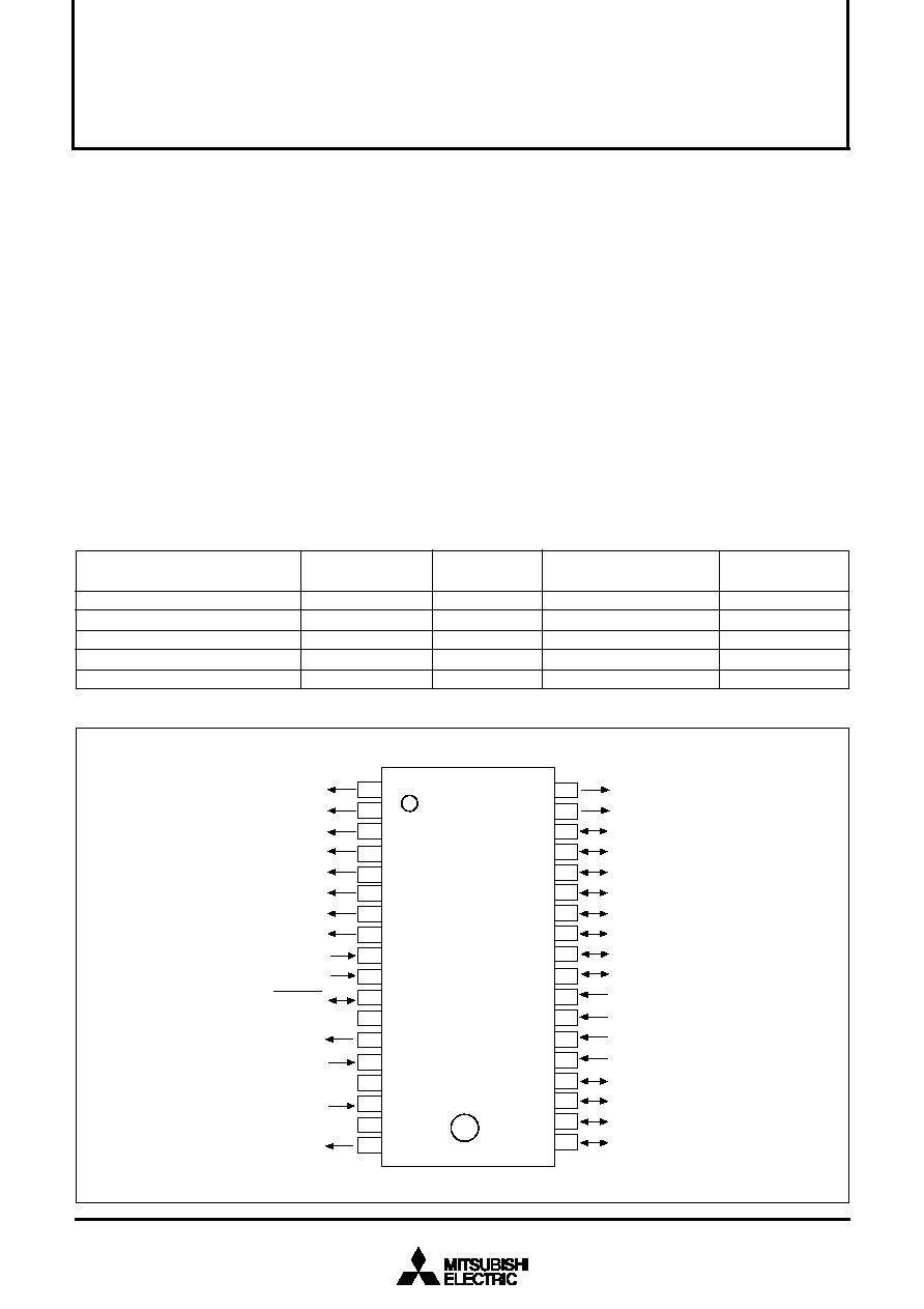
PIN CONFIGURATION (TOP VIEW)
M34570Mx-XXXFP
....................................... 2.0 V to 5.5 V (Mask ROM version)
Product
M34570M4-XXXFP
M34570M8-XXXFP
M34570MD-XXXFP
M34570E8FP
M34570EDFP *
*: Under development (Jan. 1999)
ROM type
Mask ROM
Mask ROM
Mask ROM
One Time PROM
One Time PROM
Package
36P2R-A
36P2R-A
36P2R-A
36P2R-A
36P2R-A
RAM size
(
!
4 bits)
128 words
128 words
128 words
128 words
128 words
ROM (PROM) size
(
!
10 bits)
4096 words
8192 words
16384 words
8192 words
16384 words
D
1
P4
0
P4
1
P4
2
P4
3
CNV
SS
P1
3
P1
2
P0
2
P1
0
1
2
3
4
6
7
8
9
10
11
12
14
15
16
RESET
V
DD
X
OUT
X
IN
V
SS
D
0
P0
1
P0
0
P2
0
5
13
17
18
36
35
34
33
31
30
26
25
24
23
22
21
20
19
32
27
29
28
P1
1
P0
3
P2
1
/INT
CARR
P3
2
P3
1
P3
0
VDCE
M34570Mx-XXXFP
D
3
D
5
D
4
D
7
D
6
D
8
D
9
/T
OUT
D
2
P3
3
4570 Group
SINGLE-CHIP 4-BIT CMOS MICROCOMPUTER
MITSUBISHI MICROCOMPUTERS
2
MITSUBISHI MICROCOMPUTERS
4570 Group
SINGLE-CHIP 4-BIT CMOS MICROCOMPUTER
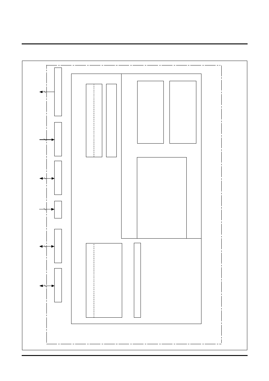
BLOCK DIAGRAM
RAM
128 words
!
4 bits
ROM (Note)
4096 to 16384 words
!
10 bits
Port P0
Port P1
4500 Series
CPU core
Memory
I/O port
Internal peripheral functions
Timers/Carrier wave generation
Timer 1 (10 bits)
Clock generating circuit
Timer 2 (8 bits)
X
IN
≠X
OUT
Watchdog timer (16 bits)
Register B (4 bits)
Register A (4 bits)
Register D (3 bits)
Register E (8 bits)
Stack registers SKs (8 levels)
Interrupt stack register SDP(1 level)
ALU(4 bits)
Port D
Port P2
10
2
4
4
Timer 3 (8 bits)
Note: PROM 16384 words
!
10 bits for the built-in PROM version.
Port P3
4
Port P4
4
(Carrier wave generation)
Reset (Voltage drop detection circuit)

3
MITSUBISHI MICROCOMPUTERS
4570 Group
SINGLE-CHIP 4-BIT CMOS MICROCOMPUTER
PERFORMANCE OVERVIEW
Function
99
1.5
µ
s (f(X
IN
) = 2.0 MHz:system clock = f(X
IN
): V
DD
= 5.0 V)
2.86
µ
s (f(X
IN
) = 4.2 MHz:system clock = f(X
IN
)/4: V
DD
= 5.0 V)
4096 words
!
10 bits
8192 words
!
10 bits
16384 words
!
10 bits
8192 words
!
10 bits
16384 words
!
10 bits
128 words
!
4 bits
Ten independent output ports; port D
9
is also used as the T
OUT
output pin.
4-bit I/O port; every pin of the ports has a key-on wakeup function and a pull-up function.
4-bit I/O port; every pin of the ports has a key-on wakeup function and a pull-up function.
2-bit input port, port P2
1
is also used as INT input pin.
4-bit I/O port
4-bit input port; both pull-up function and key-on wakeup function can be switched by software.
1-bit output port (CMOS output)
1-bit output pin; T
OUT
output pin is also used as port D
9
.
1-bit input pin with a key-on wakeup function. INT input pin is also used as port P2
1
.
10-bit timer with a reload register and carrier wave output auto-control function
8-bit timer with a reload register
8-bit timer with two reload registers and carrier wave generation function
4 (one for external and three for timer)
1 level
8 levels (however, only 7 levels can be used when an interrupt is used or the TABP p instruction
is executed)
CMOS silicon gate
36-pin plastic molded SSOP
≠20
∞
C to 70
∞
C
2.0 V to 5.5 V for mask ROM version (2.5 V to 5.5 V for One Time PROM version)
1.3 mA (f(X
IN
) = 4.2 MHz: system clock = f(X
IN
)/4, V
DD
=5.0 V)
0.5 mA (f(X
IN
) = 1.0 MHz: system clock = f(X
IN
), V
DD
=3.0 V)
0.1
µ
A (Ta=25
∞
C, V
DD
=5V, typical value)
Parameter
Number of basic instructions
Minimum instruction execution time
Memory sizes
Input/Output
ports
Timers
Interrupt
Subroutine nesting
Device structure
Package
Operating temperature range
Supply voltage
Power
dissipation
(typical value)
ROM
RAM
D
0
≠D
9
P0
0
≠P0
3
P1
0
≠P1
3
P2
0
, P2
1
P3
0
≠P3
3
P4
0
≠P4
3
CARR
T
OUT
INT
Timer 1
Timer 2
Timer 3
Sources
Nesting
at active
at RAM back-up
M34570M4
M34570M8
M34570MD
M34570E8
M34570ED
Output
I/O
I/O
Input
I/O
Input
Output
Output
Input
DEFINITION OF CLOCK AND CYCLE
q
System clock
The system clock is the basic clock for controlling this product.
The system clock can be selected by bit 3 of the clock control
register MR as shown in the table below.
Table Selection of system clock
q
Instruction clock
The instruction clock is the standard clock for controlling CPU.
The instruction clock is a signal derived from dividing the
system clock by 3. The one cycle of the instruction clock is
equivalent to the one machine cycle.
q
Machine cycle
The machine cycle is the standard cycle required to execute
the instruction.
System clock
f(X
IN
)
f(X
IN
)/4
MR
3
0
1
Note: f(X
IN
)/4 is selected immediately after system is released
from reset.

4
MITSUBISHI MICROCOMPUTERS
4570 Group
SINGLE-CHIP 4-BIT CMOS MICROCOMPUTER
PIN DESCRIPTION
Name
Power supply
Ground
CNV
SS
Reset input
Clock input
Clock output
Output port D
I/O port P0
I/O port P1
Input port P2
I/O port P3
Input port P4
Carrier wave output
for remote control
Interrupt input
Timer output
Voltage drop
detection circuit
enable
Input/Output
--
--
Input
I/O
Input
Output
Output
I/O
I/O
I/O
I/O
Input
Output
Input
Output
Input
Function
Connected to a plus power supply.
Connected to a 0 V power supply.
Connect CNV
SS
to V
SS
and apply "L" (0V) to CNV
SS
certainly.
An N-channel open-drain I/O pin for a system reset. A pull-up transistor and a
capacitor are built-in this pin. When the watchdog timer causes the system to be
reset or the low-supply voltage is detected, the RESET pin outputs "L" level.
I/O pins of the clock generating circuit. Connect a ceramic resonator between X
IN
pin and X
OUT
pin. A feedback resistor is built-in between them.
Each pin of port D has an independent 1-bit wide output function. Port D
9
is also
used as T
OUT
output pin. The output structure is N-channel open-drain.
4-bit I/O port. It can be used as an input port when the output latch is set to "1."
The output structure is N-channel open-drain. Every pin of the ports has a key-on
wakeup function and a pull-up function.
4-bit I/O port. It can be used as an input port when the output latch is set to "1."
The output structure is N-channel open-drain. Every pin of the ports has a key-on
wakeup function and a pull-up function.
2-bit input port. Port P2
1
is also used as the INT input pin.
4-bit I/O port. It can be used as an input port when the output latch is set to "1."
The output structure is N-channel open-drain.
4-bit input port. Every pin of the ports has a key-on wakeup function and a pull-up
function. Both functions can be switched by software.
Carrier wave output pin for remote control transmit. The output structure is the
CMOS circuit.
INT input pin accepts an external interrupt and has a key-on wakeup function. INT
input pin is also used as port P2
1
.
T
OUT
output pin has the function to output the timer 2 underflow signal divided by
2. T
OUT
output pin is also used as port D
9
.
VDCE pin is used to control the operation/stop of the voltage drop detection circuit.
The circuit is operating when "H" level is input to the VDCE pin. It is stopped when
"L" level is input to this pin.
Pin
V
DD
V
SS
CNV
SS
RESET
X
IN
X
OUT
D
0
≠D
9
P0
0
≠P0
3
P1
0
≠P1
3
P2
0
, P2
1
P3
0
≠P3
3
P4
0
≠P4
3
CARR
INT
T
OUT
VDCE

5
MITSUBISHI MICROCOMPUTERS
4570 Group
SINGLE-CHIP 4-BIT CMOS MICROCOMPUTER
MULTIFUNCTION
Pin
D
9
P2
1
Multifunction
T
OUT
INT
Multifunction
D
9
P2
1
Pin
T
OUT
INT
Notes 1: Pins except above have just single function.
2: The port D
9
is the output port and port P2
1
is the input port.
CONNECTIONS OF UNUSED PINS
Connection
Connect to V
SS
, or set the output latch to
"0" and open.
Set the output latch to "1" and open.
Connect to V
SS
(Note 1).
Connection
Connect to V
SS
, or set the output latch to
"0" and open.
Connect to V
SS
(Note 2) or open (Note 3).
Open.
Pin
P3
0
≠P3
3
P4
0
≠P4
3
CARR
Pin
D
0
≠D
8
D
9
/T
OUT
P0
0
≠P0
3
P1
0
≠P1
3
P2
0
, P2
1
/INT
Notes 1: When the P2
1
/INT pin is connected to V
SS
pin, set the return level to "H" level by software (interrupt control register I1
2
="1").
When the P2
1
/INT pin is connected to V
SS
pin while the return level is set to "L" level, system returns from RAM back-up
state immediately after system enters the RAM back-up state.
2: In order to connect ports P4
0
≠P4
3
to V
SS
, turn off their pull-up transistors (pull-up control register PU0i="0") by software and
also invalidate the key-on wakeup functions (key-on wakeup control register K0i="0"). When these pins are connected to
V
SS
while the key-on wakeup functions are left valid, the system fails to return from RAM back-up state. In order to make
these pins open, turn on their pull-up transistors (register PU0i="1") by software (i = 0, 1, 2, 3).
Be sure to select the key-on wakeup function and the pull-up function with every one port.
3: In order to make ports P4
0
≠P4
3
open, turn on their pull-up transistors (register PU0i = "1") by software (i = 0, 1, 2, 3).
(Note in order to set the output latch to "0" or "1" or make pins open)
∑ After system is released from reset, a port is in a high-impedance state until the output latch of the port is set to "0" by software.
Accordingly, the voltage level of pins is undefined and the excess of the supply current may occur.
∑ To set the output latch periodically is recommended because the value of output latch may change by noise or a program run away
(caused by noise).
(Note in order to connect unused pins to V
SS
)
∑ To avoid noise, connect the unused pins to V
SS
at the shortest distance using a thick wire.
PORT FUNCTION
Port
Port D
Port P0
Port P1
Port P2
Port P3
Port P4
Control
bits
1
4
4
2
4
4
Control
instructions
SD
RD
CLD
OP0A
IAP0
OP1A
IAP1
IAP2
SNZI0
(Note)
OP3A
IAP3
IAP4
Control
registers
W2
2
PU0
K0
Output structure
N-channel open-drain
N-channel open-drain
N-channel open-drain
N-channel open-drain
Remark
Pull-up functions
Key-on wakeup functions
Pull-up functions
Key-on wakeup functions
Key-on wakeup function
Pull-up functions
(programmable)
Key-on wakeup functions
(programmable)
W2
2
controls the switch of D
9
/
T
OUT
pin
Note: Level of the P2
1
/INT pin can be examined with the SNZI0 instruction.
Pin
D
0
≠D
8
, D
9
/T
OUT
P0
0
≠P0
3
P1
0
≠P1
3
P2
0
P2
1
/INT
P3
0
≠P3
3
P4
0
≠P4
3
Input/
Output
Output
(10)
I/O
(4)
I/O
(4)
Input
(2)
I/O
Input
(4)