DESCRIPTION
The M35045-XXXSP/FP is a TV screen display control IC. It uses a
silicon gate CMOS process and is housed in a 20-pin shrink DIP
package (M35045-XXXSP) or a 20-pin shrink SOP package
(M35045-XXXFP).
For M35045-001SP/FP that is a standard ROM version of M35045-
XXXSP/FP respectively, the character pattern is also mentioned.
FEATURES
∑
Screen composition .................................... 24 columns
◊
12 lines
∑
Number of characters displayed ................................... 288 (Max.)
∑
Character composition ...................................... 12
◊
18 dot matrix
∑
Characters available .............................................. 256 characters
∑
Character sizes available ..................... 4 (horizontal)
◊
4 (vertical)
∑
Display locations available
Horizontal direction .............................................. 1000 locations
Vertical direction .................................................. 1023 locations
∑
Blinking .................................................................. Character units
Cycle : division of vertical synchronization signal into 64 or 32
Duty
: 25%, 50%, or 75%
∑
Data input .................................. By the 16-bit serial input function
∑
Coloring
Character color ..................................................... Character unit
Background coloring ............................................. Character unit
Matrix-outline (shadow) coloring .............. 8 colors (RGB output)
Specified by register
Border coloring ......................................... 8 colors (RGB output)
Specified by register
Raster coloring ......................................... 8 colors (RGB output)
Specified by register
∑
Blanking
Blanking off
Character size blanking
Border size blanking
Matrix-outline blanking
All blanking (all raster area)
∑
Output ports
4 shared output ports (toggled between RGB output)
4 dedicated output ports
∑
Display RAM erase function
∑
Display input frequency range ................... F
OSC
= 30MHz-80MHz
APPLICATION
Monitor
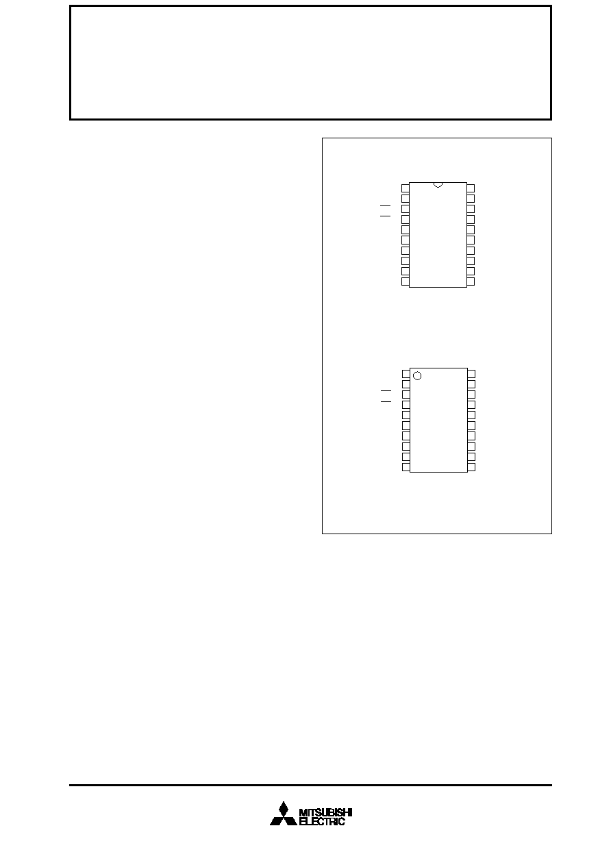
Outline 20P4B
PIN CONFIGURATION (TOP VIEW)
1
2
3
4
5
6
7
8
9
10
20
19
18
17
16
15
14
13
12
11
CPOUT
V
DD2
VERT
HOR
P5/B
P4
P3/G
P2
P1/R
P0/BLNK0
V
SS
VIR
AC
CS
SCK
SIN
TCK
V
DD1
P6
P7
M35045 - XXXSP
Outline 20P2Q-A
1
2
3
4
5
6
7
8
9
10
20
19
18
17
16
15
14
13
12
11
CPOUT
V
DD2
VERT
HOR
P5/B
P4
P3/G
P2
P1/R
P0/BLNK0
V
SS
VIR
AC
CS
SCK
SIN
TCK
V
DD1
P6
P7
M35045 - XXXFP
MITSUBISHI MICROCOMPUTERS
M35045-XXXSP/FP
SCREEN CHARACTER and PATTERN DISPLAY CONTROLLERS
2
MITSUBISHI MICROCOMPUTERS
M35045-XXXSP/FP
SCREEN CHARACTER and PATTERN DISPLAY CONTROLLERS
Symbol
CPOUT
VIR
__
AC
__
CS
SCK
SIN
TCK
V
DD1
P6
P7
V
SS
P0/BLNK0
P1/R
P2
P3/G
P4
P5/B
HOR
VERT
V
DD2
Input/
Output
Output
≠
Input
Input
Input
Input
Input
≠
Output
Output
≠
Output
Output
Output
Output
Output
Output
Input
Input
≠
Function
Connect loop filter to this pin.
Connect to GND.
When "L", this pin resets the internal IC circuit. Hysteresis input. Includes built-in pull-up
resistor.
This is the chip select pin, and when serial data transmission is being carried out, it goes
to "L". Hysteresis input. Includes built-in pull-up resistor.
__
When CS pin is "L", SIN serial data is taken in when SCK rises. Hysteresis input. Built-in
pull-up resistor is included.
This is the pin for serial input of data and addresses for the display control register and
the display data memory. Hysteresis input. Includes built-in pull-up resistor.
Input for test. Please connect to GND using circuit earthing pin.
Please connect to +5V with the power pin.
This is the output port. Port data is set by PTD6.
This is the output port. Port data is set by PTD7.
Please connect to GND using circuit earthing pin.
This pin can be toggled between port pin output and BLNK0 signal output.
This pin can be toggled between port pin output and R signal output.
This is the output port. Port data is set by PTD2.
This pin can be toggled between port pin output and G signal output.
This is the output port. Port data is set by PTD4.
This pin can be toggled between port pin output and B signal output.
This pin inputs the horizontal synchronization signal. Hysteresis input.
This pin inputs the vertical synchronization signal. Hysteresis input.
Please connect to +5V with the power pin.
Pin name
Phase difference
Frequency control
Auto-clear input
Chip select input
Serial clock input
Serial data input
Test clock
Power pin
Port P6 output
Port P7 output
Earthing pin
Port P0 output
Port P1 output
Port P2 output
Port P3 output
Port P4 output
Port P5 output
Horizontal synchro-
nization signal input
Vertical synchroni-
zation signal input
Power pin
Pin
Number
1
2
3
4
5
6
7
8
9
10
11
12
13
14
15
16
17
18
19
20
PIN DESCRIPTION
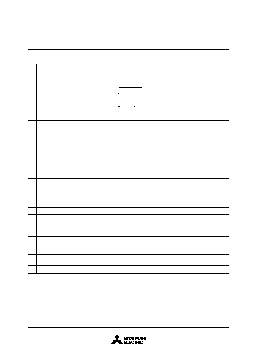
2.4k
1
0.1µF
2
4700pF
2
CPOUT
1 Use at 1% precision
2 Use at 10% precision
1pin
3
MITSUBISHI MICROCOMPUTERS
M35045-XXXSP/FP
SCREEN CHARACTER and PATTERN DISPLAY CONTROLLERS
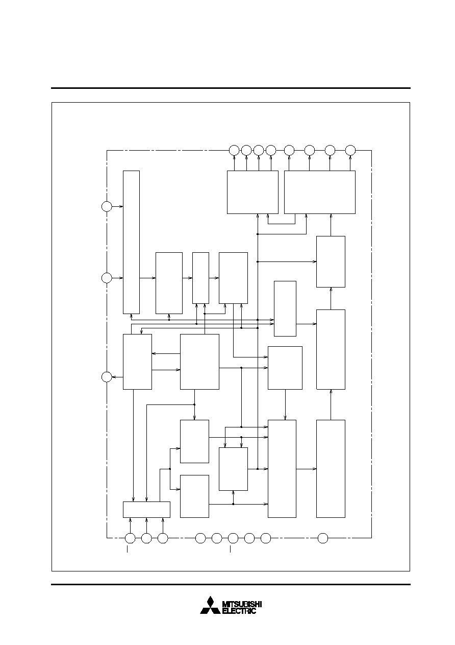
BLOCK DIAGRAM
4
1
5
6
8
20
3
11
2
7
CS
SCK
SIN
V
DD1
V
DD2
AC
V
SS
VIR
TCK
Clock oscillation
circuit for display
Timing generator
Polarity switching circuit
Address control
circuit
Data control
circuit
Display control
register
Display RAM
Display character ROM
Shift register
Blinking circuit
Reading address
control circuit
Display location
detection circuit
H counter
CPOUT
18
HOR
19
12
VERT
Synchronous signal
switching circuit
Display control
circuit
Port output
control circuit
Polarity
switching
circuti
Input control circuit
P0/BLNK0
13
P1/R
15
P3/G
17
P5/B
14
P2
16
P4
9P
6
10
P7

4
MITSUBISHI MICROCOMPUTERS
M35045-XXXSP/FP
SCREEN CHARACTER and PATTERN DISPLAY CONTROLLERS
DAF
DAE
DAD
DAC
DAB
DAA
DA9
DA8
DA7
DA6
DA5
DA4
DA3
DA2
DA1
DA0
0
BB
BG
BR
BLINK
B
G
R
C7
C6
C5
C4
C3
C2
C1
C0
0
BB
BG
BR
BLINK
B
G
R
C7
C6
C5
C4
C3
C2
C1
C0
0
0
DIVS2 DIVS1 DIVS0 DIV10
DIV9
DIV8
DIV7
DIV6
DIV5
DIV4
DIV3
DIV2
DIV1
DIV0
0
0
PTD7
PTD6
PTD5
PTD4
PTD3
PTD2
PTD1
PTD0
PTC5
PTC4
PTC3
PTC2
PTC1
PTC0
0
0
SPACE2 SPACE1 SPACE0 TEST9
HP9
HP8
HP7
HP6
HP5
HP4
HP3
HP2
HP1
HP0
0
0
TEST3 TEST2 TEST1 TEST0
VP9
VP8
VP7
VP6
VP5
VP4
VP3
VP2
VP1
VP0
0
0
TEST5 TEST4 DSP11 DSP10 DSP9
DSP8
DSP7
DSP6
DSP5
DSP4
DSP3
DSP2
DSP1
DSP0
0
0
VSZ1H1 VSZ1H0 VSZ1L1 VSZ1L0 V1SZ1 V1SZ0
LIN9
LIN8
LIN7
LIN6
LIN5
LIN4
LIN3
LIN2
0
0
VSZ2H1 VSZ2H0 VSZ2L1 VSZ2L0 V18SZ1 V18SZ0 LIN17 LIN16 LIN15 LIN14 LIN13 LIN12 LIN11 LIN10
0
0
HSZ21 HSZ20 HSZ11 HSZ10 BETA14 TEST8 TEST7 TEST6
FB
FG
FR
RB
RG
RR
0
0
BLINK2 BLINK1 BLINK0 DSPON STOP RAMERS SYAD
BLK1
BLK0
POLH POLV VMASK
__
B/F
BCOL
000
16
11F
16
120
16
121
16
122
16
123
16
124
16
125
16
126
16
127
16
128
16
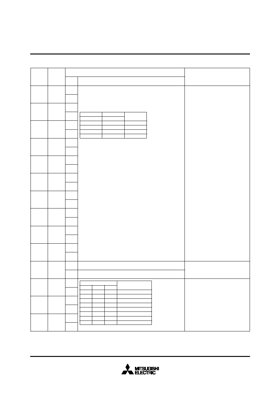
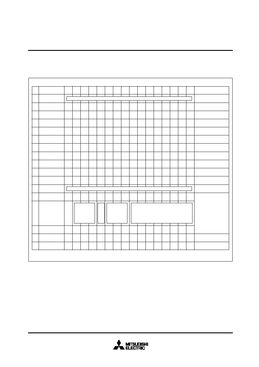
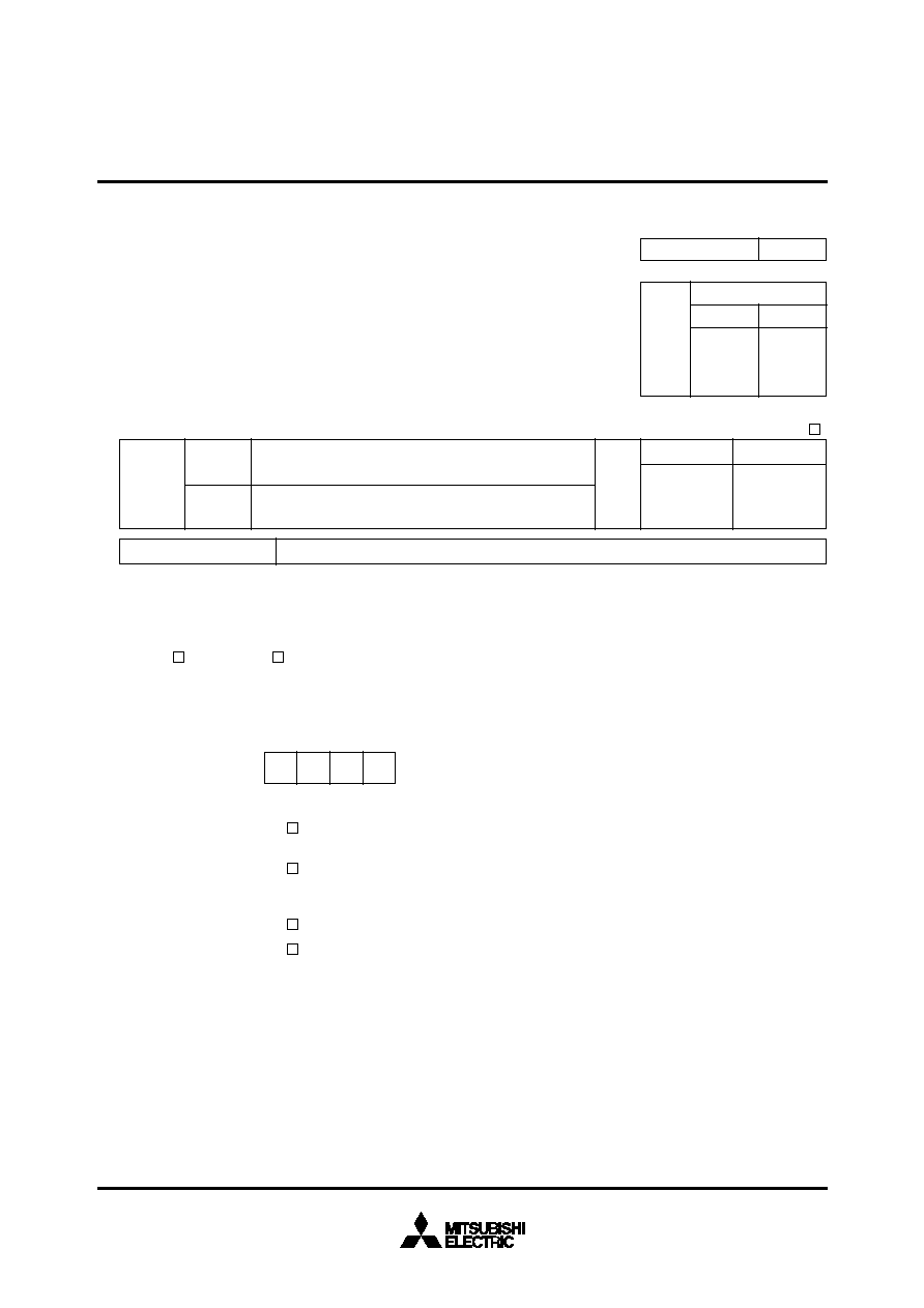
SCREEN CONSTITUTION
The screen lines and rows are determined from each address of the
display RAM. The screen constitution is shown in Figure 2.
MEMORY CONSTITUTION
Address 000
16
to 11F
16
are assigned to the display RAM, address
120
16
to 128
16
are assigned to the display control registers. The in-
ternal circuit is reset and all display control registers (address 120
16
to 128
16
) are set to "0" and display RAM (address 000
16
to 11F
16
)
__
are set to "FF
16
" when the AC pin level is "L".
Memory constitution is shown in Figure 1.
.........
.........
Background
coloring
Character color
Character code
Row
Line
1
2
3
4
5
6
7
8
9
10
11
12
000
16
001
16
002
16
003
16
004
16
005
16
006
16
007
16
008
16
009
16
00A
16
00B
16
00C
16
00D
16
00E
16
00F
16
010
16
011
16
012
16
013
16
014
16
015
16
016
16
017
16
018
16
019
16
01A
16
01B
16
01C
16
01D
16
01E
16
01F
16
020
16
021
16
022
16
023
16
024
16
025
16
026
16
027
16
028
16
029
16
02A
16
02B
16
02C
16
02D
16
02E
16
02F
16
030
16
031
16
032
16
033
16
034
16
035
16
036
16
037
16
038
16
039
16
03A
16
03B
16
03C
16
03D
16
03E
16
03F
16
040
16
041
16
042
16
043
16
044
16
045
16
046
16
047
16
048
16
049
16
04A
16
04B
16
04C
16
04D
16
04E
16
04F
16
050
16
051
16
052
16
053
16
054
16
055
16
056
16
057
16
058
16
059
16
05A
16
05B
16
05C
16
05D
16
05E
16
05F
16
060
16
061
16
062
16
063
16
064
16
065
16
066
16
067
16
068
16
069
16
06A
16
06B
16
06C
16
06D
16
06E
16
06F
16
070
16
071
16
072
16
073
16
074
16
075
16
076
16
077
16
078
16
079
16
07A
16
07B
16
07C
16
07D
16
07E
16
07F
16
080
16
081
16
082
16
083
16
084
16
085
16
086
16
087
16
088
16
089
16
08A
16
08B
16
08C
16
08D
16
08E
16
08F
16
090
16
091
16
092
16
093
16
094
16
095
16
096
16
097
16
098
16
099
16
09A
16
09B
16
09C
16
09D
16
09E
16
09F
16
0A0
16
0A1
16
0A2
16
0A3
16
0A4
16
0A5
16
0A6
16
0A7
16
0A8
16
0A9
16
0AA
16
0AB
16
0AC
16
0AD
16
0AE
16
0AF
16
0B0
16
0B1
16
0B2
16
0B3
16
0B4
16
0B5
16
0B6
16
0B7
16
0B8
16
0B9
16
0BA
16
0BB
16
0BC
16
0BD
16
0BE
16
0BF
16
0C0
16
0C1
16
0C2
16
0C3
16
0C4
16
0C5
16
0C6
16
0C7
16
0C8
16
0C9
16
0CA
16
0CB
16
0CC
16
0CD
16
0CE
16
0CF
16
0D0
16
0D1
16
0D2
16
0D3
16
0D4
16
0D5
16
0D6
16
0D7
16
0D8
16
0D9
16
0DA
16
0DB
16
0DC
16
0DD
16
0DE
16
0DF
16
0E0
16
0E1
16
0E2
16
0E3
16
0E4
16
0E5
16
0E6
16
0E7
16
0E8
16
0E9
16
0EA
16
0EB
16
0EC
16
0ED
16
0EE
16
0EF
16
0F0
16
0F1
16
0F2
16
0F3
16
0F4
16
0F5
16
0F6
16
0F7
16
0F8
16
0F9
16
0FA
16
0FB
16
0FC
16
0FD
16
0FE
16
0FF
16
100
16
101
16
102
16
103
16
104
16
105
16
106
16
107
16
108
16
109
16
10A
16
10B
16
10C
16
10D
16
10E
16
10F
16
110
16
111
16
112
16
113
16
114
16
115
16
116
16
117
16
118
16
119
16
11A
16
11B
16
11C
16
11D
16
11E
16
11F
16
1
2
3
4
5
6
7
8
9
10
11
12
13
14
15
16
17
18
19
20
21
22
23
24
*
The hexadecimal numbers in the boxes show the display RAM address.
Fig. 2
Screen constitution
Fig. 1
Memory constitution
Blink-
ing

5
MITSUBISHI MICROCOMPUTERS
M35045-XXXSP/FP
SCREEN CHARACTER and PATTERN DISPLAY CONTROLLERS
Set frequency value N2
It should be fixed to "0".
Can not be used.
0
1
0
1
0
1
0
1
0
1
0
1
0
1
0
1
0
1
0
1
0
1
0
1
0
1
0
1
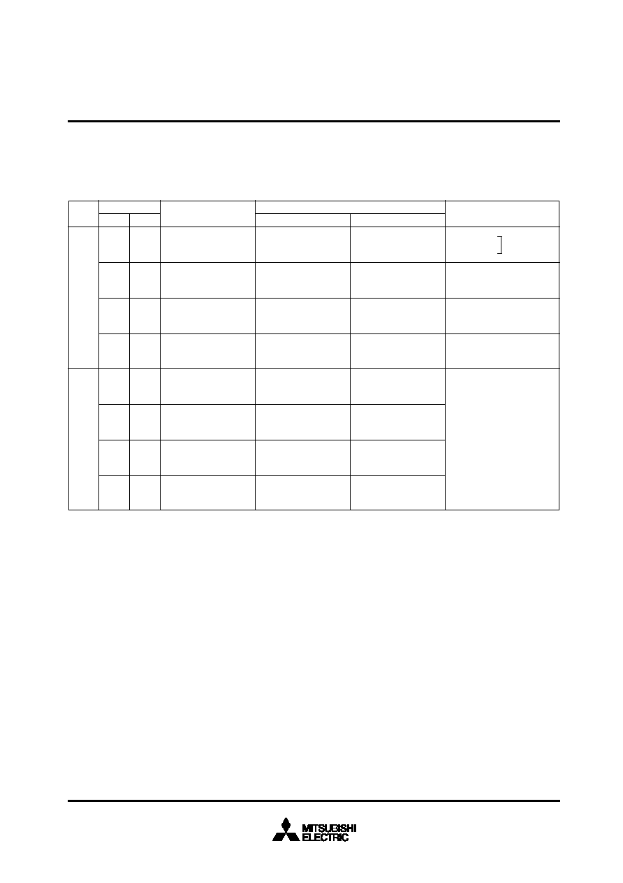
REGISTERS DESCRIPTION
(1) Address 120
16
0
1
2
3
4
5
6
7
8
9
A
B
C
D
DIV0
DIV1
DIV2
DIV3
DIV4
DIV5
DIV6
DIV7
DIV8
DIV9
DIV10
DIVS0
DIVS1
DIVS2
Set multiply value (frequency value) of horizontal synchronous fre-
quency.
N1 = (DIVn
◊
2
n
)
N1: frequency value
Display frequency is computed as
shown below.
F
OSC
= f
H
◊
N1
F
OSC
[MHz] : Display frequency
f
H
[kHz]
: Horizontal synchronous
signal frequency to HOR
pin.
N1
: Shown left
Set display frequency F
OSC
to within
30MHz to 80MHz range.
When display frequency F
OSC
, set fre-
quency value N2 in association with
DIVS0 and DIVS1.
__
Note: The mark
/
around the status value means the reset status by the "L" level is input to AC pin.
Set frequency value N2 in association
with display frequency range.
10
n = 0
0
0
1
0
1
1
0
0
1
1
DIVS
Frequency
value N2
Display frequency
55 ~ 80
40 ~ 55
30 ~ 40
Register
DA
Status
Contents
Function
Remarks
Frequency value N2
Division into 2
Division into 3
Division into 4
Division into 2
Division into 3
Division into 4
Do not set
6
MITSUBISHI MICROCOMPUTERS
M35045-XXXSP/FP
SCREEN CHARACTER and PATTERN DISPLAY CONTROLLERS
BLNK0 outputs blanking signal.
Blanking status is determined by BLK0,
BLK1, and DSP0 to DSP11 settings.
P0 pin data control.
P1 pin data control.
P2 pin exclusive port output state con-
trol.
P3 pin data control.
P4 pin exclusive port output state con-
trol.
P5 pin data control.
P6 pin exclusive port output state con-
trol.
P7 pin exclusive port output state con-
trol.
0
1
0
1
0
1
0
1
0
1
0
1
0
1
0
1
0
1
0
1
0
1
0
1
0
1
0
1
(2) Address 121
16
0
1
2
3
4
5
6
7
8
9
A
B
C
D
PTC0
PTC1
PTC2
PTC3
PTC4
PTC5
PTD0
PTD1
PTD2
PTD3
PTD4
PTD5
PTD6
PTD7
P0 output (port P0). Port data is set by PTD0.
BLNK0 output. Polarity is set by PTD0.
P1 output (port P1). Port data is set by PTD1.
R signal output. Polarity is set by PTD1.
P2 output (port P2). Port data is set by PTD2.
Do not set.
P3 output (port P3). Port data is set by PTD3.
G signal output. Polarity is set by PTD3.
P4 output (port P4). Port data is set by PTD4.
Do not set.
P5 output (port P5). Port data is set by PTD5.
B signal output. Polarity is set by PTD5.
"L" output (P0 output) or negative polarity output (BLNK0 output).
"H" output (P0 output) or positive polarity output (BLNK0 output).
"L" output (P1 output) or negative polarity output (R signal output).
"H" output (P1 output) or positive polarity output (R signal output).
"L" output (P2 output).
"H" output (P2 output).
"L" output (P3 output) or negative polarity output (G signal output).
"H" output (P3 output) or positive polarity output (G signal output).
"L" output (P2 output).
"H" output (P2 output).
"L" output (P5 output) or negative polarity output (B signal output).
"H" output (P5 output) or positive polarity output (B signal output).
"L" output (P6 output).
"H" output (P6 output).
"L" output (P7 output).
"H" output (P7 output).
Register
DA
Status
Contents
Function
Remarks
7
MITSUBISHI MICROCOMPUTERS
M35045-XXXSP/FP
SCREEN CHARACTER and PATTERN DISPLAY CONTROLLERS
(3) Address 122
16
Horizontal display start location is
specified using the 10 bits from HP9
to HP0.
Note: HP9 to 0 = (0000000000
2
) and
(0000010111
2
) setting is forbidden
0
1
0
1
0
1
0
1
0
1
0
1
0
1
0
1
0
1
0
1
0
1
0
1
0
1
0
1
Register
Function
Remarks
DA
Status
Contents
0
1
2
3
4
5
6
7
8
9
A
B
C
D
If HS is the horizontal display start location,
HS = T
◊
(
2
n
HP
n
+ N).
T: The cycle of display frequency
Leave one line worth of space in the ver-
tical direction.
For example, 6
Õ
6 indicates two sets
of 6 lines with a line of spaces between
lines 6 and 7.
A line is 18
◊
N horizontal scan lines.
N is determined by the character size in
the vertical direction as follows:
◊
1 N = 1
◊
2 N = 2
◊
3 N = 3
◊
4 N = 4
HP1
HP2
HP3
HP4
HP5
HP6
HP7
HP8
TEST9
SPACE0
SPACE1
SPACE2
HP9
(MSB)
HP0
(LSB)
SPACE
2
0
0
0
0
1
1
1
1
1
0
0
1
1
0
0
1
1
0
0
1
0
1
0
1
0
1
Number of Lines and Space
(
Õ
represents space)
12
1
Õ
10
Õ
1
2
Õ
8
Õ
2
3
Õ
6
Õ
3
4
Õ
4
Õ
4
5
Õ
2
Õ
5
6
Õ
6
6
Õ
Õ
6
Õ
represents one line worth of spaces.
9
n = 0
1000 settings are possible.
HSZ10
HSZ20
0
1
0
1
HSZ11
HSZ21
0
0
1
1
N
6
7
8
9
It should be fixed to "0".
Can not be used.
8
MITSUBISHI MICROCOMPUTERS
M35045-XXXSP/FP
SCREEN CHARACTER and PATTERN DISPLAY CONTROLLERS
(4) Address 123
16
The vertical start location is specified
using the 10 bits from VP9 to VP0.
VP9 to VP0 = (0000000000
2
) setting is
forbidden.
_
Note 1: In case of B/F register is "0".
0
1
0
1
0
1
0
1
0
1
0
1
0
1
0
1
0
1
0
1
0
1
0
1
0
1
0
1
Register
DA
Status
Contents
0
1
2
3
4
5
6
7
8
9
A
B
C
D
VP1
VP2
VP3
VP4
VP5
VP6
VP7
VP8
TEST0
TEST1
TEST2
TEST3
If VS is the vertical display start location,
VS = H
◊
(
2
n
VP
n
).
H: Cycle with the horizontal synchronizing pulse
1023 settings are possible.
VP9
(MSB)
VP0
(LSB)
Function
Remarks
9
n = 0
It should be fixed to "0".
Can not be used.
It should be fixed to "0".
Can not be used.
It should be fixed to "0".
Can not be used.
It should be fixed to "0".
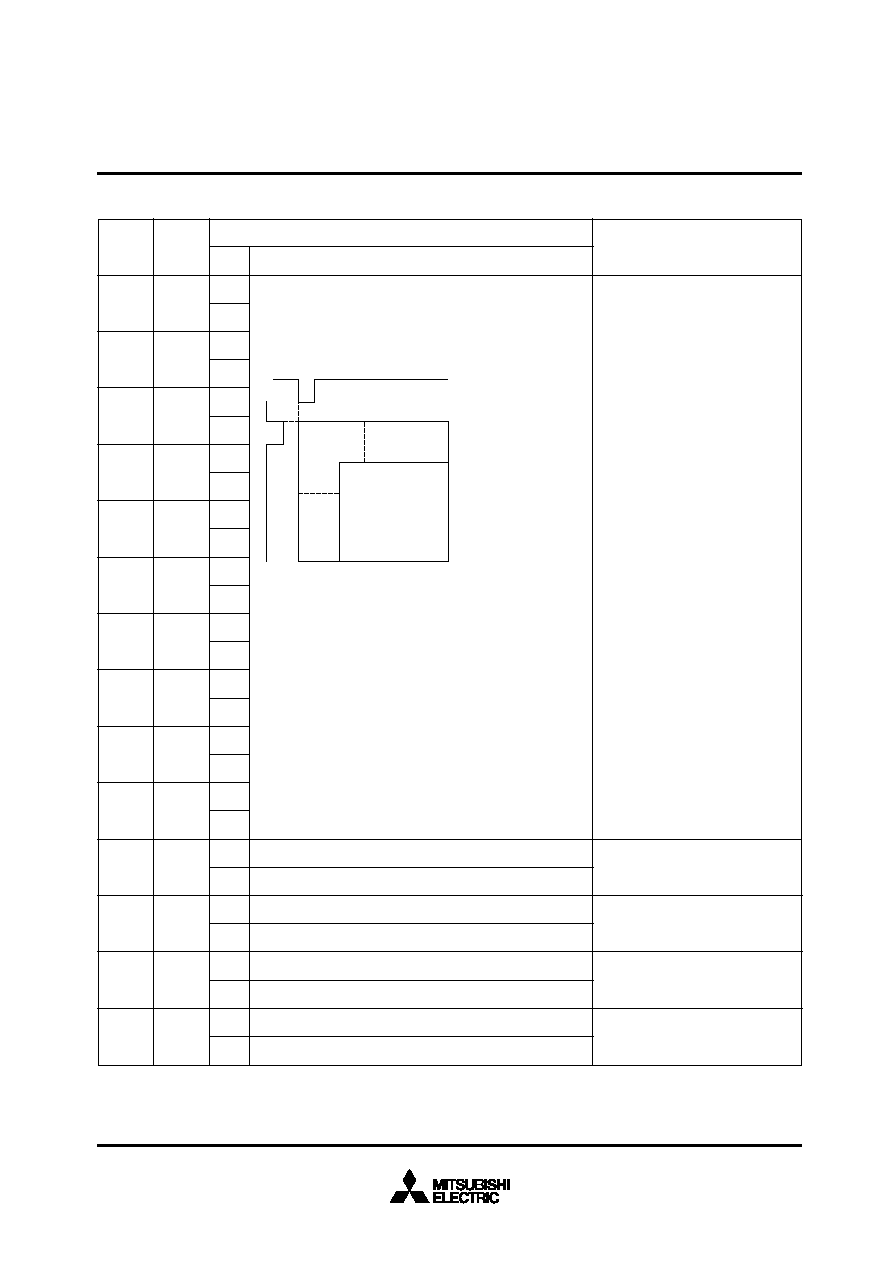
Can not be used.
HOR
VERT
Character
displaying area
VP
HP

9
MITSUBISHI MICROCOMPUTERS
M35045-XXXSP/FP
SCREEN CHARACTER and PATTERN DISPLAY CONTROLLERS
Sets the display mode of line 1.
Sets the display mode of line 2.
Sets the display mode of line 3.
Sets the display mode of line 4.
Sets the display mode of line 5.
Sets the display mode of line 6.
Sets the display mode of line 7.
Sets the display mode of line 8.
Sets the display mode of line 9.
Sets the display mode of line 10.
Sets the display mode of line 11.
Sets the display mode of line 12.
0
1
0
1
0
1
0
1
0
1
0
1
0
1
0
1
0
1
0
1
0
1
0
1
0
1
0
1
(5) Address 124
16
0
1
2
3
4
5
6
7
8
9
A
B
C
D
DSP0
DSP1
DSP2
DSP3
DSP4
DSP5
DSP6
DSP7
DSP8
DSP9
DSP10
DSP11
TEST4
TEST5
Blanking is in the display mode specified by BLK0 and BLK1. (Note)
Blanking is in the display mode specified by except BLK0 and BLK1.
Blanking is in the display mode specified by BLK0 and BLK1. (Note)
Blanking is in the display mode specified by except BLK0 and BLK1.
Blanking is in the display mode specified by BLK0 and BLK1. (Note)
Blanking is in the display mode specified by except BLK0 and BLK1.
Blanking is in the display mode specified by BLK0 and BLK1. (Note)
Blanking is in the display mode specified by except BLK0 and BLK1.
Blanking is in the display mode specified by BLK0 and BLK1. (Note)
Blanking is in the display mode specified by except BLK0 and BLK1.
Blanking is in the display mode specified by BLK0 and BLK1. (Note)
Blanking is in the display mode specified by except BLK0 and BLK1.
Blanking is in the display mode specified by BLK0 and BLK1. (Note)
Blanking is in the display mode specified by except BLK0 and BLK1.
Blanking is in the display mode specified by BLK0 and BLK1. (Note)
Blanking is in the display mode specified by except BLK0 and BLK1.
Blanking is in the display mode specified by BLK0 and BLK1. (Note)
Blanking is in the display mode specified by except BLK0 and BLK1.
Blanking is in the display mode specified by BLK0 and BLK1. (Note)
Blanking is in the display mode specified by except BLK0 and BLK1.
Blanking is in the display mode specified by BLK0 and BLK1.
Blanking is in the display mode specified by except BLK0 and BLK1.
Blanking is in the display mode specified by BLK0 and BLK1.
Blanking is in the display mode specified by except BLK0 and BLK1.
It should be fixed to "0".
Can not be used.
It should be fixed to "0".
Can not be used.
Register
DA
Status
Contents
Function
Remarks
Note: Refer to DISPLAY FORM1.
10
MITSUBISHI MICROCOMPUTERS
M35045-XXXSP/FP
SCREEN CHARACTER and PATTERN DISPLAY CONTROLLERS
Character size setting in the vertical
direction for the 2nd line.
Character size setting in the vertical
direction for the 3rd line.
Character size setting in the vertical
direction for the 4th line.
Character size setting in the vertical
direction for the 5th line.
Character size setting in the vertical
direction for the 6th line.
Character size setting in the vertical
direction for the 7th line.
Character size setting in the vertical
direction for the 8th line.
Character size setting in the vertical
direction for the 9th line.
Character size setting in the vertical
direction for the 1st line.
(display monitor 1 ~ 12 line)
Character size setting in the vertical
direction (display monitor 1 line) at "0"
state in register LIN2 ~ LIN17.
Character size setting in the vertical
direction (display monitor 1 line) at "1"
state in register LIN2 ~ LIN17.
0
1
0
1
0
1
0
1
0
1
0
1
0
1
0
1
0
1
0
1
0
1
0
1
0
1
0
1
(6) Address 125
16
0
1
2
3
4
5
6
7
8
9
A
B
C
D
LIN2
LIN3
LIN4
LIN5
LIN6
LIN7
LIN8
LIN9
V1SZ0
V1SZ1
VSZ1L0
VSZ1L1
VSZ1H0
VSZ1H1
Register
DA
Status
Contents
Function
Remarks
The first line is set by VSZ1L0 and VSZ1L1.
The second to 12th lines are set by VSZ2L0 and VSZ2L1.
The first line is set by VSZ1H0 and VSZ1H1.
The second to 12th lines are set by VSZ2H0 and VSZ2H1.
The first line is set by VSZ1L0 and VSZ1L1.
The second to 12th lines are set by VSZ2L0 and VSZ2L1.
The first line is set by VSZ1H0 and VSZ1H1.
The second to 12th lines are set by VSZ2H0 and VSZ2H1.
The first line is set by VSZ1L0 and VSZ1L1.
The second to 12th lines are set by VSZ2L0 and VSZ2L1.
The first line is set by VSZ1H0 and VSZ1H1.
The second to 12th lines are set by VSZ2H0 and VSZ2H1.
The first line is set by VSZ1L0 and VSZ1L1.
The second to 12th lines are set by VSZ2L0 and VSZ2L1.
The first line is set by VSZ1H0 and VSZ1H1.
The second to 12th lines are set by VSZ2H0 and VSZ2H1.
The first line is set by VSZ1L0 and VSZ1L1.
The second to 12th lines are set by VSZ2L0 and VSZ2L1.
The first line is set by VSZ1H0 and VSZ1H1.
The second to 12th lines are set by VSZ2H0 and VSZ2H1.
The first line is set by VSZ1L0 and VSZ1L1.
The second to 12th lines are set by VSZ2L0 and VSZ2L1.
The first line is set by VSZ1H0 and VSZ1H1.
The second to 12th lines are set by VSZ2H0 and VSZ2H1.
The first line is set by VSZ1L0 and VSZ1L1.
The second to 12th lines are set by VSZ2L0 and VSZ2L1.
The first line is set by VSZ1H0 and VSZ1H1.
The second to 12th lines are set by VSZ2H0 and VSZ2H1.
The first line is set by VSZ1L0 and VSZ1L1.
The second to 12th lines are set by VSZ2L0 and VSZ2L1.
The first line is set by VSZ1H0 and VSZ1H1.
The second to 12th lines are set by VSZ2H0 and VSZ2H1.
H: Cycle with the horizontal synchronizing pulse
V1SZ1
0
0
1
1
V1SZ0
0
1
0
1
Vertical direction size
1H/dot
2H/dot
3H/dot
4H/dot
H: Cycle with the horizontal synchronizing pulse
VSZ1L1
0
0
1
1
VSZ1L0
0
1
0
1
Vertical direction size
1H/dot
2H/dot
3H/dot
4H/dot
H: Cycle with the horizontal synchronizing pulse
VSZ1H1
0
0
1
1
VSZ1H0
0
1
0
1
Vertical direction size
1H/dot
2H/dot
3H/dot
4H/dot

11
MITSUBISHI MICROCOMPUTERS
M35045-XXXSP/FP
SCREEN CHARACTER and PATTERN DISPLAY CONTROLLERS
Character size setting in the vertical
direction for the 10th line.
Character size setting in the vertical
direction for the 11th line.
Character size setting in the vertical
direction for the 12th line.
Character size setting in the vertical
direction for the 13th line.
Character size setting in the vertical
direction for the 14th line.
Character size setting in the vertical
direction for the 15th line.
Character size setting in the vertical
direction for the 16th line.
Character size setting in the vertical
direction for the 17th line.
Character size setting in the vertical
direction for the 18th line.
(display monitor 1 ~ 12 line)
Character size setting in the vertical
direction (display monitor for 2 ~ 12 line)
at "0" state in register LIN2 ~ LIN17.
Character size setting in the vertical
direction (display monitor for 2 ~ 12 line)
at "1" state in register LIN2 ~ LIN17.
0
1
0
1
0
1
0
1
0
1
0
1
0
1
0
1
0
1
0
1
0
1
0
1
0
1
0
1
(7) Address 126
16
0
1
2
3
4
5
6
7
8
9
A
B
C
D
LIN10
LIN11
LIN12
LIN13
LIN14
LIN15
LIN16
LIN17
V18SZ0
V18SZ1
VSZ2L0
VSZ2L1
VSZ2H0
VSZ2H1
Register
DA
Status
Contents
Function
Remarks
The first line is set by VSZ1L0 and VSZ1L1.
The second to 12th lines are set by VSZ2L0 and VSZ2L1.
The first line is set by VSZ1H0 and VSZ1H1.
The second to 12th lines are set by VSZ2H0 and VSZ2H1.
The first line is set by VSZ1L0 and VSZ1L1.
The second to 12th lines are set by VSZ2L0 and VSZ2L1.
The first line is set by VSZ1H0 and VSZ1H1.
The second to 12th lines are set by VSZ2H0 and VSZ2H1.
The first line is set by VSZ1L0 and VSZ1L1.
The second to 12th lines are set by VSZ2L0 and VSZ2L1.
The first line is set by VSZ1H0 and VSZ1H1.
The second to 12th lines are set by VSZ2H0 and VSZ2H1.
The first line is set by VSZ1L0 and VSZ1L1.
The second to 12th lines are set by VSZ2L0 and VSZ2L1.
The first line is set by VSZ1H0 and VSZ1H1.
The second to 12th lines are set by VSZ2H0 and VSZ2H1.
The first line is set by VSZ1L0 and VSZ1L1.
The second to 12th lines are set by VSZ2L0 and VSZ2L1.
The first line is set by VSZ1H0 and VSZ1H1.
The second to 12th lines are set by VSZ2H0 and VSZ2H1.
The first line is set by VSZ1L0 and VSZ1L1.
The second to 12th lines are set by VSZ2L0 and VSZ2L1.
The first line is set by VSZ1H0 and VSZ1H1.
The second to 12th lines are set by VSZ2H0 and VSZ2H1.
The first line is set by VSZ1L0 and VSZ1L1.
The second to 12th lines are set by VSZ2L0 and VSZ2L1.
The first line is set by VSZ1H0 and VSZ1H1.
The second to 12th lines are set by VSZ2H0 and VSZ2H1.
The first line is set by VSZ1L0 and VSZ1L1.
The second to 12th lines are set by VSZ2L0 and VSZ2L1.
The first line is set by VSZ1H0 and VSZ1H1.
The second to 12th lines are set by VSZ2H0 and VSZ2H1.
H: Cycle with the horizontal synchronizing pulse
V18SZ1
0
0
1
1
V18SZ0
0
1
0
1
Vertical direction size
1H/dot
2H/dot
3H/dot
4H/dot
H: Cycle with the horizontal synchronizing pulse
VSZ2L1
0
0
1
1
VSZ2L0
0
1
0
1
Vertical direction size
1H/dot
2H/dot
3H/dot
4H/dot
H: Cycle with the horizontal synchronizing pulse
VSZ2H1
0
0
1
1
VSZ2H0
0
1
0
1
Vertical direction size
1H/dot
2H/dot
3H/dot
4H/dot
12
MITSUBISHI MICROCOMPUTERS
M35045-XXXSP/FP
SCREEN CHARACTER and PATTERN DISPLAY CONTROLLERS
Color
Black
Red
Green
Yellow
Blue
Magenta
Cyan
White
Sets the color of all blankings.
Sets the blanking color of the Border
size, or the shadow size.
Set this register to the character font
set by display RAM BR, BG and BB.
Character size setting in the vertical
direction for the first line.
Character size setting in the vertical
direction for the 2nd line to 12th line.
0
1
0
1
0
1
0
1
0
1
0
1
0
1
0
1
0
1
0
1
0
1
0
1
0
1
0
1
(8) Address 127
16
0
1
2
3
4
5
6
7
8
9
A
B
C
D
RR
RG
RB
FR
FG
FB
TEST6
TEST7
TEST8
BETA14
HSZ10
HSZ11
HSZ20
HSZ21
Register
DA
Status
Contents
Function
Remarks
T: Display frequency cycle
HSZ11
0
0
1
1
HSZ10
0
1
0
1
Vertical direction size
1T/dot
2T/dot
3T/dot
4T/dot
T: Display frequency cycle
VSZ21
0
0
1
1
HSZ20
0
1
0
1
Vertical direction size
1T/dot
2T/dot
3T/dot
4T/dot
It should be fixed to "0".
Can not be used.
It should be fixed to "0".
Can not be used.
It should be fixed to "0".
Can not be used.
Matrix-outline display (12
◊
18 dot)
Matrix-outline display (14
◊
18 dot)
RB
0
0
0
0
1
1
1
1
RG
0
0
1
1
0
0
1
1
RR
0
1
0
1
0
1
0
1
Color
Black
Red
Green
Yellow
Blue
Magenta
Cyan
White
BB
0
0
0
0
1
1
1
1
BG
0
0
1
1
0
0
1
1
BR
0
1
0
1
0
1
0
1

13
MITSUBISHI MICROCOMPUTERS
M35045-XXXSP/FP
SCREEN CHARACTER and PATTERN DISPLAY CONTROLLERS
Blanking of BLK0, BLK1
All raster blanking
Synchronize with the leading edge of horizontal synchronization.
Synchronize with the trailing edge of horizontal synchronization.
Do not mask by VERT input signal
Mask by VERT input signal
VERT pin polarity is negative electrode
VERT pin polarity is positive electrode
HOR pin polarity is negative electrode
HOR pin polarity is positive electrode
Border display of character
Shadow display of character
RAM not erased
RAM erased
Oscillation of clock for display
Stop the oscillation of clock for display
Display OFF
Display ON
Divided into 64 of vertical synchronous signal
Divided into 32 of vertical synchronous signal
Sets all raster blanking
Synchronize with the front porch or
back porch of the horizontal
synchronazation signal.
This register has or do not have mask
at phase comparison operating.
Set VERT pin polarity.
Set HOR pin polarity.
Set blanking mode. (Note 1)
An example of blanking mode at
BCOL = "0", DSPn = "0" (n = 0 ~ 11)
shown left.
(Note 2)
There is no need to reset because
there is no register for this bit.
R, G, B and BLNK0 output can be
altered.
Display can be altered.
Blinking duty ratio can be altered.
Blinking frequency can be altered.
0
1
0
1
0
1
0
1
0
1
0
1
0
1
0
1
0
1
0
1
0
1
0
1
0
1
0
1
(9) Address 128
16
0
1
2
3
4
5
6
7
8
9
A
B
C
D
BCOL
__
B/F
VMASK
POLV
POLH
BLK0
BLK1
SYAD
RAMERS
STOP
DSPON
BLINK0
BLINK1
BLINK2
Register
DA
Status
Contents
Function
Remarks
BLINK
1
0
0
1
1
0
0
1
0
1
Duty
Blinking OFF
25%
50%
75%
1
0
0
1
1
0
0
1
0
1
Blanking mode
Matrix-outline size
Character size
Border size
Matrix-outline size
Notes 1: Refer to DISPLAY FORM 1
2: Refer to DISPLAY FORM 3
BLK
14
MITSUBISHI MICROCOMPUTERS
M35045-XXXSP/FP
SCREEN CHARACTER and PATTERN DISPLAY CONTROLLERS
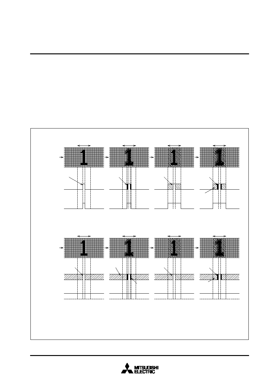
DISPLAY FORM1
Table 1 shows display form of blanking.
0
0
1
1
0
0
1
1
0
1
0
1
0
1
0
1
Table 1. Display mode
DSPn = 1
1
(Note 1)
All blanking size
DSPn = "0" line
Matrix-outline size
DSPn = "1" line
DSPn = "0" line
Character size
DSPn = "1" line
Border size
DSPn = "0" line
Border size
DSPn = "1" line
Matrix-outline size
DSPn = "0" line
Matrix-outline size
DSPn = "1" line
Character size
Matrix-outline display
color set: display RAM
(Note 3)
Border display
color set: display RAM
(Note 3)
Matrix-outline display
color set: display RAM
(Note 3)
Character
Matrix-outline display
color set: display RAM
(Note 3)
Border display
color set: display RAM
(Note 3)
Matrix-outline display
color set: display RAM
(Note 3)
Character
BCOL
Standard blanking
When the all of registers
DSPn (Note 2) are set to "0"
Matrix-outline and border display.
color set: FR, FG, FB
or display RAM (Note 4)
Character
Border display
color set: display RAM
(Note 3)
Matrix-outline display
color set: display RAM
(Note 3)
Matrix-outline and border display.
color set: FR, FG, FB
or display RAM (Note 4)
Character
Border display
color set: display RAM
(Note 3)
Matrix-outline display
color set: display RAM
(Note 3)
Matrix-outline and border display.
color set: FR, FG, FB
or display RAM (Note 4)
Character
Border display
color set: display RAM
(Note 3)
Matrix-outline display
color set: display RAM
(Note 3)
Matrix-outline and border display.
color set: FR, FG, FB
or display RAM (Note 4)
Character
Border display
color set: display RAM
(Note 3)
Matrix-outline display
color set: display RAM
(Note 3)
When some of registers DSPi are set to "1"
DSPn = 0
BLNK0 output
BLK0
BLK1
0
Notes 1: Color setting of raster area is set by register RR, RG and RB.
2: DSPn (n = 0 ~ 11)
3: Set by BR, BG and BB of
display RAM
.
4: Set border by register FR, FG and FB. Set matrix-outline by BR, BG and BB of
display RAM
.
15
MITSUBISHI MICROCOMPUTERS
M35045-XXXSP/FP
SCREEN CHARACTER and PATTERN DISPLAY CONTROLLERS
Fig. 3
Display form
12dots
12dots
12dots
12dots
Set character color by display
RAM
1
(address 0 to 11F
16
)
Scanning
Scanning
Set border
color by register
FR,FG and FB
Set border color by
display RAM
1
Set border color by
display RAM
1
Set matrix - outline
color by display
RAM
3
Set matrix - outline
color by RAM
for display
3
R,G or B output
BLNK0 output
(1) Character display
(character size)
2
(2) Border display
(border size)
(3) Matrix - outline
display
(matrix-outline size)
(4) Matrix - outline
and border display
(matrix-outline size)
12dots
12dots
12dots
12dots
Set character color by display
RAM
1
(address 0 to 11F
16
)
Set border
color by register
FR,FG and FB
Set raster area
color by register
RR,RG and RB
Set matrix - outline
color by display
RAM
3
Set matrix - outline
color by display
RAM
3
R,G or B output
BLNK0 output
(1) Character display
(all blanking size)
2
(2) Border display
(all blanking size)
(3) Matrix - outline
display
(all blanking size)
(4) Matrix - outline
and border display
(all blanking size)
1 Red,Blue,Yellow,Green,Magenta,Cyan, White and Black are set possible.
2 ( ) is blanking mode.
3 All matrix - outline horizontal direction size is able to set to 14dots by register BETA14
(BLNK0 output by 14dots).
Register BCOL = "0"
Register BCOL = "1"
"H" level
GND level
Display form 2
M35045-XXXSP has the following four display forms.
(1) Character size
: Blanking same as the character size.
(2) Border size
: Blanking the background as a size from character.
(3) Matrix-outline size
: Blanking the background 12
◊
18 dot.
When set register BETA14 to "1", setting of blanking the
background 14
◊
18 dot is possible.
(4) All blanking size
: When set register BCOL to "1", all raster area is blanking.
16
MITSUBISHI MICROCOMPUTERS
M35045-XXXSP/FP
SCREEN CHARACTER and PATTERN DISPLAY CONTROLLERS
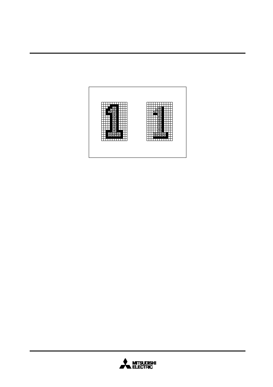
Display form 3
When border display mode, if set SYAD = "0" to "1", it change to
shadow display mode.
Border and shadow display are shown below.
Fig. 4
Border and shadow display
Set shadow display color by display RAM or register FR, FG and FB.
Border display
Shadow display
17
MITSUBISHI MICROCOMPUTERS
M35045-XXXSP/FP
SCREEN CHARACTER and PATTERN DISPLAY CONTROLLERS
DAF DAE DAD DAC DAB DAA DA9 DA8 DA7 DA6 DA5 DA4 DA3 DA2 DA1 DA0
0
0
0
0
0
0
0
1
0
0
1
0
0
0
0
0
0
0
0
DIVS1 DIVS0 DIV10 DIV9 DIV8 DIV7 DIV6 DIV5 DIV4 DIV3 DIV2 DIV1 DIV0
0
0
PTD7 PTD6
1
PTD4
1
PTD2
1
1
1
0
1
0
1
1
0
0
0
0
0
0
HP9 HP8 HP7 HP6 HP5 HP4 HP3 HP2 HP1 HP0
0
0
0
0
0
0
VP9 VP8 VP7 VP6 VP5 VP4 VP3 VP2 VP1 VP0
0
0
0
0
0
0
0
0
0
0
0
0
0
0
0
0
0
0
0
0
0
0
0
0
0
0
0
0
0
0
0
0
0
0
0
0
0
0
0
0
0
0
0
0
0
0
0
0
0
0
0
0
0
0
0
0
0
0
0
0
0
0
0
0
0
0
0
0
0
0
0
1
0
1
1
POLH POLV
0
0
0
0
BB
BG
BR BLINK
B
G
R
C7
C6
C5
C4
C3
C2
C1
C0
0
BB
BG
BR BLINK
B
G
R
C7
C6
C5
C4
C3
C2
C1
C0
0
0
0
0
0
0
0
1
0
0
1
0
1
0
0
0
0
0
0
0
0
1
0
0
0
1
1
POLH POLV
0
0
0
1
2
3
4
5
6
7
8
9
10
11
12
297
298
299
300
DATA INPUT EXAMPLE
Data of display RAM and display control registers can be set by the
serial input function. Example of data setting is shown in Figure 5.
Example of data setting by the serial input function (M35045-XXXSP/FP)
address 120
16
data
120
16
data
121
16
data
122
16
data
123
16
data
124
16
data
125
16
data
126
16
data
127
16
data
128
16
data
000
16
data
11F
16
address 128
16
data
128
16
200 msec hold
200 msec hold
.........
............
............
Character
background
color
Character
color
Character code
Notes 1: Input horizontal synchronous signal to HOR pin.
2: Matrix-outline display in this data.
Fig. 5
Example of data setting by the serial input function
Addition
System set-up
Address set
Setting frequency
dividing value (Note 1)
Output setting
Horizontal display
location setting
Vertical display
location setting
Display form setting
Character size setting
Character size setting
Color,
character size setting
Display OFF,
display form (Note 2)
Character setting
Address setting
Display ON, display
form (Note 2)
Blink-
ing
18
MITSUBISHI MICROCOMPUTERS
M35045-XXXSP/FP
SCREEN CHARACTER and PATTERN DISPLAY CONTROLLERS
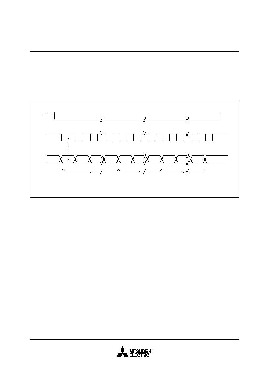
SERIAL DATA INPUT TIMING
(1)
Serial data should be input with the LSB first.
(2)
The address consists of 16 bits.
(3)
The data consists of 16 bits.
(4)
__
The 16 bits in the SCK after the CS signal has fallen are the
address, and for succeeding input data, the address is
incremented every 16 bits.
Fig. 6
Serial input timing
CS
N = 1,2,3.........
SCK
SIN
LSB
MSB
LSB
MSB
LSB
MSB
Address(16 bits)
Data(16 bits)
N
Data(16 bits)
N + 1

19
MITSUBISHI MICROCOMPUTERS
M35045-XXXSP/FP
SCREEN CHARACTER and PATTERN DISPLAY CONTROLLERS
CHARACTER FONT
Images are composed on a 12
◊
18 dot matrix, and characters can
be linked vertically and horizontally with other characters to allow the
display the continuous symbols.
Fig. 7
Example for displaying a continuous pattern after combining characters in the horizontal or vertical direction
Character code FF
16
is fixed as a blank without background.
Therefore, you cannot register a character font in this code.
When the character extends
to the top line of the matrix,
no border is left at the top.
When the character extends
to the bottom(18th) line of
the matrix, no border is left
at the bottom.
Note : Hatching represents
border.
18 dots
12 dots
20
MITSUBISHI MICROCOMPUTERS
M35045-XXXSP/FP
SCREEN CHARACTER and PATTERN DISPLAY CONTROLLERS
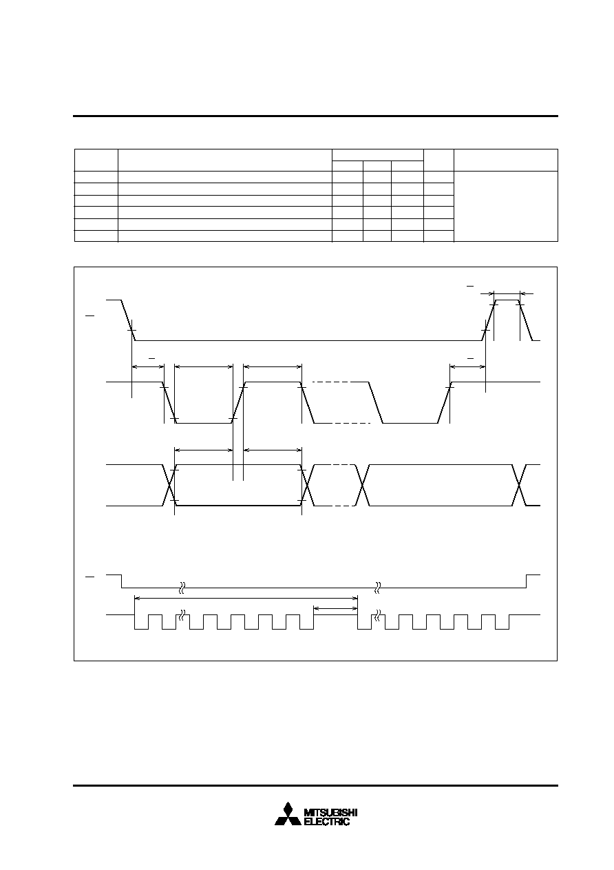
Symbol
t
w
(SCK)
__
t
su(CS)
__
t
h(CS)
t
su(SIN)
t
h(SIN)
t
word
TIMING REQUIREMENTS
(Ta = ≠20∞C to + 85∞C, V
DD
= 5±0.25V, unless otherwise noted)
Unit
ns
ns
µs
ns
ns
Parameter
SCK width
__
CS setup time
__
CS hold time
SIN setup time
SIN hold time
1 word writing time
Min.
200
200
2
200
200
10
Typ.
--
--
--
--
--
--
Max.
--
--
--
--
--
--
Remarks
See Figure 8
Limits
Fig. 8
Serial input timing requirements
t
su(CS)
t
w(SCK)
t
w(SCK)
t
su(SIN)
t
h(SIN)
t
h(CS)
t
w(CS)
1
m
s(min.)
t
word
more than 2 µs
1
2
12
13
14
15
16
...
1
12
13
14
15
16
...
CS
SCK
SIN
SCK
CS
µs
21
MITSUBISHI MICROCOMPUTERS
M35045-XXXSP/FP
SCREEN CHARACTER and PATTERN DISPLAY CONTROLLERS
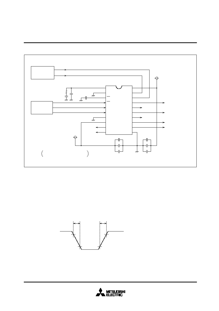
EXAMPLE OF THE M35045-XXXSP/FP CLOCK PERIPHERAL CIRCUIT
Fig. 9
Example of the M35045-XXXSP peripheral circuit (M35045-XXXFP peripheral circuit is same as that of M35045-XXXSP)
Note for waveform timing of the horizontal sig-
nals to the HOR pin.
Set horizontal synchronous signal edge
waveform timing to under
5ns and input to HOR pin.
_
Set only the side which set by B/F register waveform timing under
5ns and input to HOR pin.
_
: Set front porch edge or back porch edge by B/F register.
Synchronous signal
generator
+ 5V
+ 5V
100µF
1µF
0.01µF
100µF
1µF
0.01µF
Microcomputer
Horizontal synchronous signal (5V)
Vertical synchronous signal (5V)
CPOUT
1
VIR
4700pF(Note2)
2.4k
(Note1)
0.1
m
F(Note2)
2
AC
3
CS
4
SCK
5
SIN
6
TCK
7
V
DD1
8
P6
9
P7
10
20
19
18
17
16
15
14
13
12
11
V
DD2
VERT
HOR
P5/B
P4
P3/G
P2
P1/R
P0/BLNK0
V
SS
M35045 - XXXSP
+ ≠
1µF
+ ≠
≠ +
B
BLNK0
G
R
Mixing
video pre - amp
Note 1 : Use this 1% precision element.
Note 2 : Use this 10% precision element.
Horizontal synchronous signal input
90%
10%
tf
tr
22
MITSUBISHI MICROCOMPUTERS
M35045-XXXSP/FP
SCREEN CHARACTER and PATTERN DISPLAY CONTROLLERS
Unit
V
mA
V
V
k
Symbol
V
DD
V
I
V
O
P
d
T
opr
T
stg
ABSOLUTE MAXIMUM RATINGS
Parameter
Supply voltage
Input voltage
Output voltage
Power dissipation
Operating temperature
Storage temperature
Conditions
With respect to V
SS
.
Ta = 25∞C
Ratings
≠0.3 to +6.0
V
SS
≠0.3
<
V
I
<
V
DD
+0.3
V
SS
<
V
O
<
V
DD
300
≠20 to +85
≠40 to +125
Unit
V
V
V
mW
∞C
∞C
Typ.
5.0
V
DD
0
--
Min.
4.75
0.8V
DD
0
30.0
Parameter
Supply voltage
__
__
"H" level input voltage SIN, SCK, CS, AC HOR, VERT
__
__
"L" level input voltage SIN, SCK, CS, AC HOR, VERT
Oscillating frequency for display
Max.
5.25
V
DD
0.2V
DD
80.0
Limits
RECOMMENDED OPERATING CONDITIONS
(V
DD
= 5V, Ta = ≠20 to +85∞C, unless otherwise noted)
Symbol
V
DD
V
IH
V
IL
F
OSC
Unit
V
V
V
MHz
ELECTRICAL CHARACTERISTICS
(V
DD
= 5V, Ta = 25∞C, unless otherwise noted)
Symbol
V
DD
I
DD
V
OH
V
OL
R
I
Parameter
Supply voltage
Supply current
"H" level output voltage
"L" level output voltage
__
__
Pull-up resistance SCK, AC, CS, SIN
Test conditions
Ta = ≠20 to +85∞C
V
DD
= 5.25V
V
DD
= 4.75V, I
OH
= 0.4mA
V
DD
= 4.75V, I
OH
= 0.05mA
V
DD
= 4.75V, I
OL
= 0.4mA
V
DD
= 4.75V, I
OL
= 0.05mA
V
DD
= 5.0V
Limits
Min.
4.75
--
3.5
--
10
Typ.
5.0
30
--
--
30
Max.
5.25
50
--
0.4
100
P0 ~ P7
CPOUT
P0 ~ P7
CPOUT
23
MITSUBISHI MICROCOMPUTERS
M35045-XXXSP/FP
SCREEN CHARACTER and PATTERN DISPLAY CONTROLLERS
Note for Supplying Power
__
Timing of power supplying to AC pin
The internal circuit of M35045-XXXSP/FP is reset when the level of
__
the auto clear input pin AC is "L". This pin in hysteresis input with the
__
pull-up resistor. The timing about power supplying of AC pin is shown
in Figure 10.
Timing of power supplying to V
DD1
and V
DD2
.
Supply power to V
DD1
and V
DD2
at the same time.
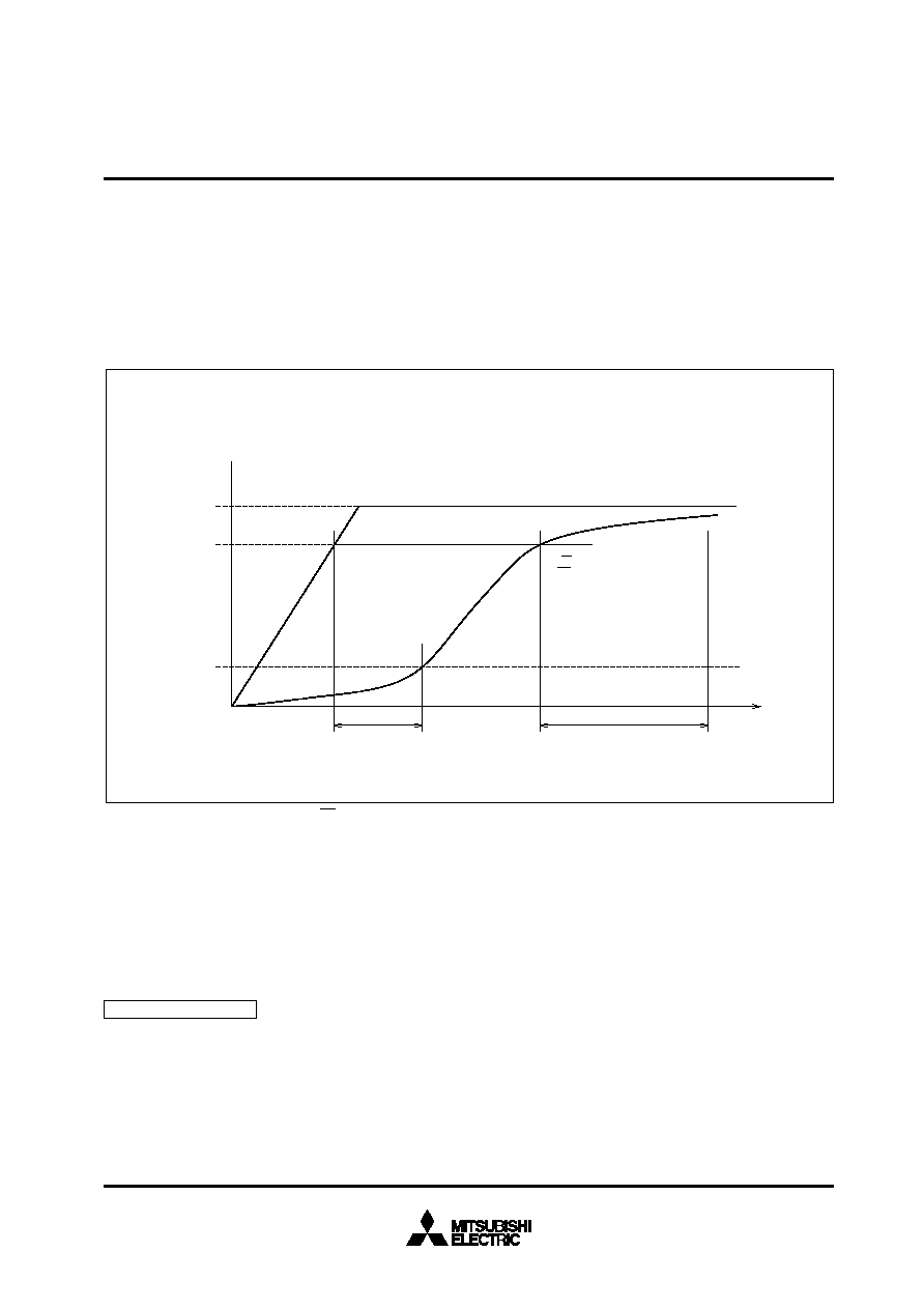
Fig. 10 Timing of power supplying to AC pin
DATA REQUIRED FOR MASK ROM ORDERING
Please send the following data for mask orders.
(1) M35045-XXXSP/FP mask ROM order confirmation form
(2) 20P4B mask specification form
(3) ROM data (EPROM 3 sets)
(4) Floppy disks containing the character font generating program
+ character data
Supply voltage
V
AC
(AC pin input voltage)
0.8
◊
V
DD
0.2
◊
V
DD
t
W
t
S
V
DD
Time t
[
s
]
more than 1ms
Voltage
[V]
After supplying the power (V
DD
and V
SS
) to M35045-XXXSP/FP and
the supply voltage becomes more than 0.8
◊
V
DD
, it needs to keep
__
V
IL
time; tw of the AC pin for more than 1ms.
__
Start inputting from microcomputer after AC pin supply voltage
becomes more than 0.8
!
V
DD
and keeping 200ms wait time.
PRECAUTION FOR USE
Notes on noise and latch-up
In order to avoid noise and latch-up, connect a bypass capacitor
(
0.1µF) directly between the V
DD1
pin and V
SS
pin, and the V
DD2
pin
and V
SS
pin using a heavy wire.
MITSUBISHI MICROCOMPUTERS
M35045-XXXSP/FP
SCREEN CHARACTER and PATTERN DISPLAY CONTROLLERS
24
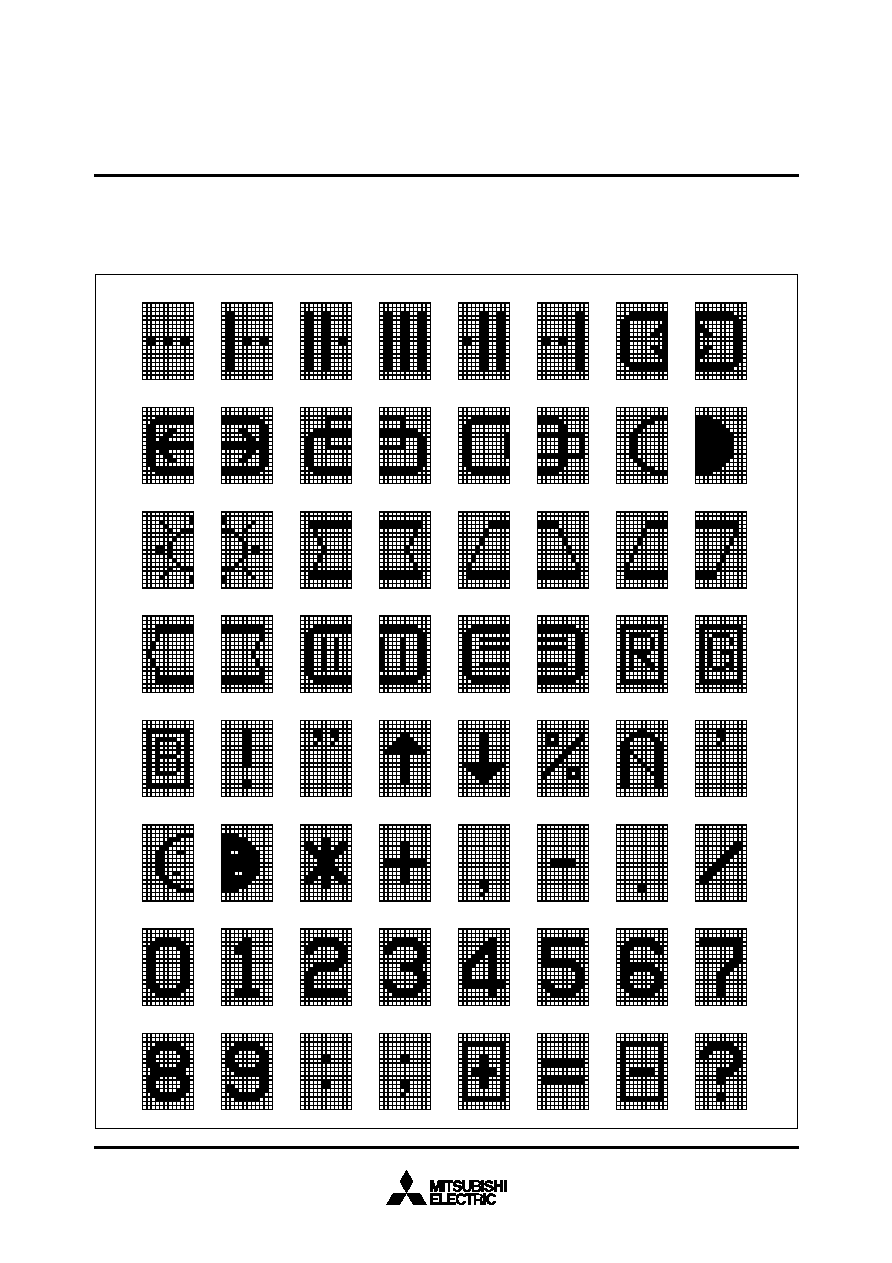
Fig. 11 M35045-002SP/FP character patterns (1)
STANDARD ROM TYPE : M35045-002SP/FP
M35045-002SP/FP is a standard ROM type of M35045-XXXSP/FP.
The character patterns are fixed to the contents of Figure
11 to 16.
38
16
39
16
3A
16
3B
16
3C
16
3D
16
3E
16
3F
16
00
16
01
16
02
16
03
16
04
16
05
16
06
16
07
16
08
16
09
16
0A
16
0B
16
0C
16
0D
16
0E
16
0F
16
10
16
11
16
12
16
13
16
14
16
15
16
16
16
17
16
18
16
19
16
1A
16
1B
16
1C
16
1D
16
1E
16
1F
16
20
16
21
16
22
16
23
16
24
16
25
16
26
16
27
16
28
16
29
16
2A
16
2B
16
2C
16
2D
16
2E
16
2F
16
30
16
31
16
32
16
33
16
34
16
35
16
36
16
37
16
38
16
39
16
3A
16
3B
16
3C
16
3D
16
3E
16
3F
16

MITSUBISHI MICROCOMPUTERS
M35045-XXXSP/FP
SCREEN CHARACTER and PATTERN DISPLAY CONTROLLERS
25
Fig. 12 M35045-002SP/FP character patterns (2)
40
16
41
16
42
16
43
16
44
16
45
16
46
16
47
16
48
16
49
16
4A
16
4B
16
4C
16
4D
16
4E
16
4F
16
50
16
51
16
52
16
53
16
54
16
55
16
56
16
57
16
58
16
59
16
5A
16
5B
16
5C
16
5D
16
5E
16
5F
16
60
16
61
16
62
16
63
16
64
16
65
16
66
16
67
16
68
16
69
16
6A
16
6B
16
6C
16
6D
16
6E
16
6F
16
70
16
71
16
72
16
73
16
74
16
75
16
76
16
77
16
78
16
79
16
7A
16
7B
16
7C
16
7D
16
7E
16
7F
16
MITSUBISHI MICROCOMPUTERS
M35045-XXXSP/FP
SCREEN CHARACTER and PATTERN DISPLAY CONTROLLERS
26
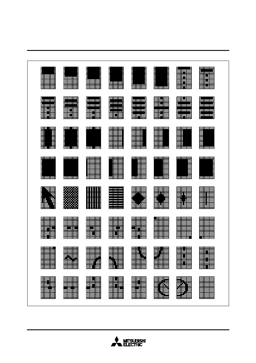
Fig. 13. M35045-002SP/FP character patterns (3)
80
16
81
16
82
16
83
16
84
16
85
16
86
16
87
16
88
16
89
16
8A
16
8B
16
8C
16
8D
16
8E
16
8F
16
90
16
91
16
92
16
93
16
94
16
95
16
96
16
97
16
98
16
99
16
9A
16
9B
16
9C
16
9D
16
9E
16
9F
16
A0
16
A1
16
A2
16
A3
16
A4
16
A5
16
A6
16
A7
16
A8
16
A9
16
AA
16
AB
16
AC
16
AD
16
AE
16
AF
16
B0
16
B1
16
B2
16
B3
16
B4
16
B5
16
B6
16
B7
16
B8
16
B9
16
BA
16
BB
16
BC
16
BD
16
BE
16
BF
16
MITSUBISHI MICROCOMPUTERS
M35045-XXXSP/FP
SCREEN CHARACTER and PATTERN DISPLAY CONTROLLERS
27
Fig. 14 M35045-002SP/FP character patterns (4)
C0
16
C1
16
C2
16
C3
16
C4
16
C5
16
C6
16
C7
16
C8
16
C9
16
CA
16
CB
16
CC
16
CD
16
CE
16
CF
16
D0
16
D1
16
D2
16
D3
16
D4
16
D5
16
D6
16
D7
16
D8
16
D9
16
DA
16
DB
16
DC
16
DD
16
DE
16
DF
16
E0
16
E1
16
E2
16
E3
16
E4
16
E5
16
E6
16
E7
16
E8
16
E9
16
EA
16
EB
16
EC
16
ED
16
EE
16
EF
16
F0
16
F1
16
F2
16
F3
16
F4
16
F5
16
F6
16
F7
16
F8
16
F9
16
FA
16
FB
16
FC
16
FD
16
FE
16
FF
16
blank
MITSUBISHI MICROCOMPUTERS
M35045-XXXSP/FP
SCREEN CHARACTER and PATTERN DISPLAY CONTROLLERS
28
Receipt
Data :
Supervisor
signature
Section head
signature
Mask ROM number
Company
name
Date :
TEL
(
)
Issuance
signature
Note : Please fill in all items marked
g
,
.
g
g
g
Remarks
q
Return the Character Font Preparation Program after use.
q
Three EPROMs are required. Specify the type of EPROMs submitted. (All the three EPROMs must be same types.
Check @ in the appropriate box.)
27256
27512
(1) The font data prepared by the Character Font Preparation Program is saved as a binary type object file
(addresses 0000
h
to 7FFF
h
). Three sets of these EPROMs are required.
(2) Attach the erase protect seals on three EPROMs. Each seal bears the type name (M35045), and ROM No.
(≠...SP/FP).
q
Write the checksum code (hexadecimal notation) for entire EPROM areas.
Checksum
q
Select the marking type (Check @ in the appropriate box).
Special mark
....... Fill in the Mark Specification Form (20P4B for M35045-XXXSP, 20P2Q-A for
M35045-XXXFP) and attach to the Mask ROM Order Confirmation Form.
Standard Mark
....... No writing is required.
q
The package type
....... SDIP type (M35045-XXXSP)
....... SSOP type (M35045-XXXFP)
g q
Comments
Customer
Data
issued
Program version name
M045R V
GZZ-SH00-36B<65Aÿ>
MASK ROM ORDER CONFIRMATION FORM
SCREEN DISPLAY IC M35045-XXXSP/FP
MITSUBISHI ELECTRIC
Supervisor
Responsible
officer
(1/6)

MITSUBISHI MICROCOMPUTERS
M35045-XXXSP/FP
SCREEN CHARACTER and PATTERN DISPLAY CONTROLLERS
29
Mask ROM number
GZZ-SH00-36B<65Aÿ>
g
2. Character patterns (The patterns with the mark "#" are test patterns)
(See the next page)
(2/6)
#
#
#
#
#
#
#
#

MITSUBISHI MICROCOMPUTERS
M35045-XXXSP/FP
SCREEN CHARACTER and PATTERN DISPLAY CONTROLLERS
30
00
16
01
16
02
16
03
16
04
16
05
16
06
16
07
16
08
16
09
16
0A
16
0B
16
0C
16
0D
16
0E
16
0F
16
10
16
11
16
12
16
13
16
14
16
15
16
16
16
17
16
18
16
19
16
1A
16
1B
16
1C
16
1D
16
1E
16
1F
16
(3/6)
20
16
21
16
22
16
23
16
24
16
25
16
26
16
27
16
28
16
29
16
2A
16
2B
16
2C
16
2D
16
2E
16
2F
16
30
16
31
16
32
16
33
16
34
16
35
16
36
16
37
16
38
16
39
16
3A
16
3B
16
3C
16
3D
16
3E
16
3F
16

MITSUBISHI MICROCOMPUTERS
M35045-XXXSP/FP
SCREEN CHARACTER and PATTERN DISPLAY CONTROLLERS
31
40
16
41
16
42
16
43
16
44
16
45
16
46
16
47
16
48
16
49
16
4A
16
4B
16
4C
16
4D
16
4E
16
4F
16
50
16
51
16
52
16
53
16
54
16
55
16
56
16
57
16
58
16
59
16
5A
16
5B
16
5C
16
5D
16
5E
16
5F
16
60
16
61
16
62
16
63
16
64
16
65
16
66
16
67
16
68
16
69
16
6A
16
6B
16
6C
16
6D
16
6E
16
6F
16
70
16
71
16
72
16
73
16
74
16
75
16
76
16
77
16
78
16
79
16
7A
16
7B
16
7C
16
7D
16
7E
16
7F
16
(4/6)
MITSUBISHI MICROCOMPUTERS
M35045-XXXSP/FP
SCREEN CHARACTER and PATTERN DISPLAY CONTROLLERS
32
80
16
81
16
82
16
83
16
84
16
85
16
86
16
87
16
88
16
89
16
8A
16
8B
16
8C
16
8D
16
8E
16
8F
16
90
16
91
16
92
16
93
16
94
16
95
16
96
16
97
16
98
16
99
16
9A
16
9B
16
9C
16
9D
16
9E
16
9F
16
A0
16
A1
16
A2
16
A3
16
A4
16
A5
16
A6
16
A7
16
A8
16
A9
16
AA
16
AB
16
AC
16
AD
16
AE
16
AF
16
B0
16
B1
16
B2
16
B3
16
B4
16
B5
16
B6
16
B7
16
B8
16
B9
16
BA
16
BB
16
BC
16
BD
16
BE
16
BF
16
(5/6)

MITSUBISHI MICROCOMPUTERS
M35045-XXXSP/FP
SCREEN CHARACTER and PATTERN DISPLAY CONTROLLERS
33
C0
16
C1
16
C2
16
C3
16
C4
16
C5
16
C6
16
C7
16
C8
16
C9
16
CA
16
CB
16
CC
16
CD
16
CE
16
CF
16
D0
16
D1
16
D2
16
D3
16
D4
16
D5
16
D6
16
D7
16
D8
16
D9
16
DA
16
DB
16
DC
16
DD
16
DE
16
DF
16
E0
16
E1
16
E2
16
E3
16
E4
16
E5
16
E6
16
E7
16
E8
16
E9
16
EA
16
EB
16
EC
16
ED
16
EE
16
EF
16
F0
16
F1
16
F2
16
F3
16
F4
16
F5
16
F6
16
F7
16
F8
16
F9
16
FA
16
FB
16
FC
16
FD
16
FE
16
FF
16
Blank
(6/6)

MITSUBISHI MICROCOMPUTERS
M35045-XXXSP/FP
SCREEN CHARACTER and PATTERN DISPLAY CONTROLLERS
34
20P2Q-A (20-PIN SHRINK SOP) MARK SPECIFICATION FORM

MITSUBISHI MICROCOMPUTERS
M35045-XXXSP/FP
SCREEN CHARACTER and PATTERN DISPLAY CONTROLLERS
35
20P4B (20-PIN DIP) MARK SPECIFICATION FORM
MITSUBISHI MICROCOMPUTERS
M35045-XXXSP/FP
SCREEN CHARACTER and PATTERN DISPLAY CONTROLLERS
36
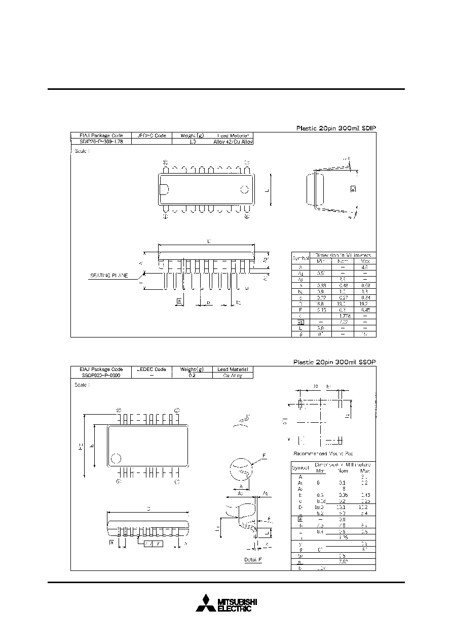
PACKAGE OUTLINE
20P2Q-A
20P4B

MITSUBISHI MICROCOMPUTERS
M35045-XXXSP/FP
SCREEN CHARACTER and PATTERN DISPLAY CONTROLLERS
Dec. First Edition 1996 H-DF463-A
Editioned by
Committee of editing of Mitsubishi Semiconductor Data Book
Published by
Mitsubishi Electric Corp., Semiconductor Division
This book, or parts thereof, may not be reproduced in any form without permission of
Mitsubishi Electric Corporation.
©1996 MITSUBISHI ELECTRIC CORPORATION Printed in Japan
MITSUBISHI DATA BOOK
SINGLE-CHIP 4-BIT MICROCOMPUTERS
Enlarged
edition