M35053-XXXSP/FP
SCREEN CHARACTER and PATTERN DISPLAY CONTROLLERS
MITSUBISHI MICROCOMPUTERS
DESCRIPTION
The M35053-XXXSP/FP is TV screen display control IC which can
be used to display information such as number of channels, the date
and messages and program schedules on the TV screen.
In particular, owing to the built-in SYNC-SEP (synchronous separa-
tion) circuit, the synchronous correction circuit, the Decoder circuit,
and to the Encoder circuit, external circuits can be decrease and
character turbulence that occurs when superimposing can be reduced.
The processor can conform to the EDS broadcast service and is suit-
able for AV systems such as VTRs, LDs, and so on.
It is a silicon gate CMOS process and M35053-XXXSP is housed in
a 20-pin shrink DIP package, M35053-XXXFP is housed in a 20-pin
shrink SOP package.
For M35053-001SP/FP that is a standard ROM version of M35053-
XXXSP/FP respectively, the character pattern is also mentioned.
FEATURES
∑
Screen composition .............................. 24 characters
!
10 lines,
32 characters
!
7 lines
∑
Number of characters displayed .................................. 240 (Max.)
∑
Character composition ..................................... 12
!
18 dot matrix
∑
Characters available ............................................. 256 characters
∑
Character sizes available .................... 4 (horizontal)
!
4 (vertical)
∑
Display locations available
Horizontal direction ............................................... 240 locations
Vertical direction ................................................... 256 locations
∑
Blinking ................................................................. Character units
Cycle : approximately 1 second, or approximately 0.5 seconds
Duty : 25%, 50%, or 75%
∑
Data input .............................. By the serial input function (16 bits)
∑
Coloring
Background coloring (composite video signal)
∑
Blanking
Total blanking (14
!
18 dots)
Border size blanking
Character size blanking
∑
Synchronizing signal
Composite synchronizing signal generation
(PAL, NTSC, M-PAL)
∑
2 output ports (1 digital line)
∑
Oscillation stop function
It is possible to stop the oscillation for synchronizing signal
generation
∑
Built-in half-tone display function
∑
Built-in reversed character display function
∑
Built-in Decoder (NTSC only)
∑
Built-in Encoder (NTSC only)
∑
Built-in synchronous correction circuit
∑
Built-in synchronous separation circuit
APPLICATION
TV, VCR, Movie
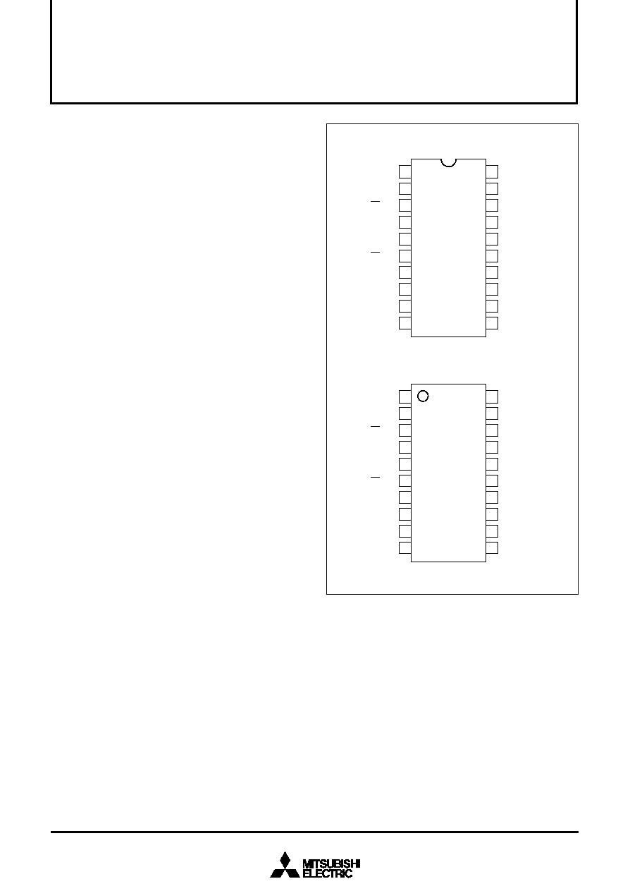
PIN CONFIGURATION (TOP VIEW)
REV.1.1
M35053-XXXFP
20
19
18
17
16
15
14
13
12
11
1
2
3
4
5
6
7
8
9
10
CP1
TESTA
CS
SCK
SIN
AC
V
DD2
CVIDEO
LECHA
CVIN
V
DD1
HOR
CP2
OSCIN
V
SS
P1
P0
TESTB
EDO
V
SS
M35053-XXXSP
20
19
18
17
16
15
14
13
12
11
1
2
3
4
5
6
7
8
9
10
CP1
TESTA
CS
SCK
SIN
AC
V
DD2
CVIDEO
LECHA
CVIN
V
DD1
HOR
CP2
OSCIN
V
SS
P1
P0
TESTB
EDO
V
SS
Outline 20P4B
Outline 20P2Q-A
M35053-XXXSP/FP
SCREEN CHARACTER and PATTERN DISPLAY CONTROLLERS
MITSUBISHI MICROCOMPUTERS
2
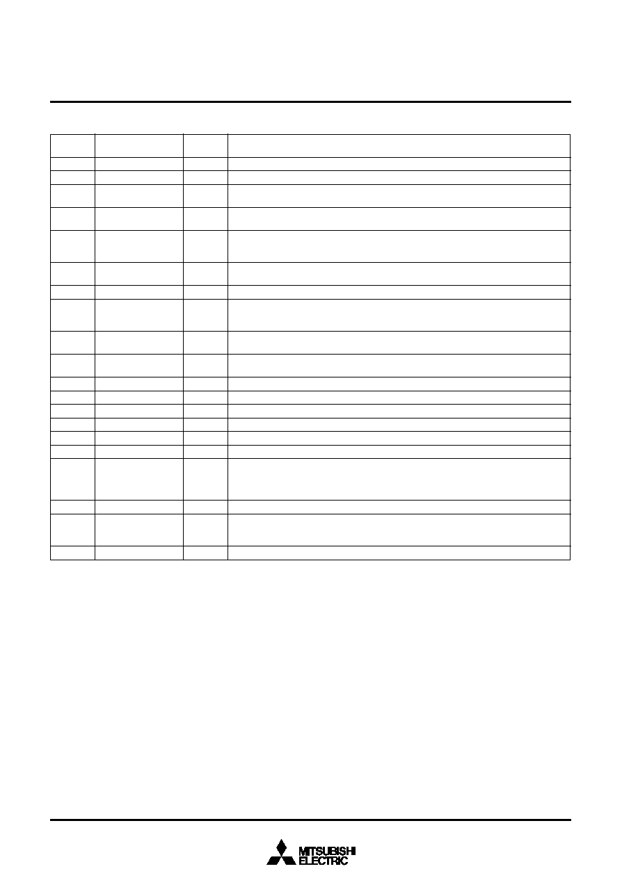
PIN DESCRIPTION
Function
This is the filter output pin 1.
This is the pin for test. Connect this pin to GND during normal operation.
This is the chip select pin, and when serial data transmission is being carried out, it goes
to "L". Hysteresis input. Includes built-in pull-up resistor.
__
When CS pin is "L", SIN serial data is taken in when SCK rises. Hysteresis input. Built-in
pull-up resistor is included.
This is the pin for serial input of data and addresses for the display control register and
the display data memory. Also, serially outputs decode data according to the settings in
the relevant registers (serial I/O).
When "L", this pin resets the internal IC circuit. Hysteresis input. Includes built-in pull-up
resistor.
Please connect to +5V with the analog circuit power pin.
This is the output pin for composite video signals. It outputs 2V
P-P
composite video
signals. In superimpose mode, character output etc. is superimposed on the external
composite video signals from CVIN.
This is the input pin which determines the "white" character color level in the composite
video signal.
This is the input pin for external composite video signals. In superimpose mode, character
output etc. is superimposed on these external composite video signals.
Please connect to GND using circuit earthing pin.
This is the output pin for encode data. It outputs digital three-value data or composite video signals.
This is the pin for test. Connect this pin to GND during normal operation.
This pin outputs the port output or BLNK1 (character background) signal.
This pin outputs the port output or CO1(character) signal.
Please connect to GND using circuit earthing pin (Analog side).
This is the input pin for the sub-carrier frequency (f
SC
) for generating a synchronous
signal.
A frequency of 3.580MHz is needed for NTSC, and a frequency of 4.434MHz in needed
for PAL and 3.576MHz is needed for M-PAL.
Filter output pin 2.
This is the input pin for external composite video signals. This pin inputs the external
video signal clamped sync-chip to 1.5V, and internally carries out synchronous separa-
tion.
Please connect to +5V with the digital circuit power pin.
Symbol
OSC1
TESTA
__
CS
SCK
SIN
__
AC
V
DD2
CVIDEO
LECHA
CVIN
V
SS
EDO
TESTB
P0
P1
V
SS
OSCIN
CP2
HOR
V
DD1
Pin name
Clock input
Test pin
Chip select input
Serial clock input
Serial data input/
output
Auto-clear input
Power pin
Composite video
signal output
Character level input
Composite video
signal input
Earthing pin
Encode data output
Test pin
Port P0 output
Port P1 output
Earthing pin
f
SC
input pin for
synchronous signal
generation
Filter output
Horizontal synchro-
nizing signal input
Power pin
Input/
Output
Input
--
Input
Input
Input/
Output
Input
--
Output
Input
Input
--
Output
--
Output
Output
--
Input
Output
Input
--

M35053-XXXSP/FP
SCREEN CHARACTER and PATTERN DISPLAY CONTROLLERS
MITSUBISHI MICROCOMPUTERS
3
BLOCK DIAGRAM
Data
control
circuit
Address
control
circuit
Displa
y control
register
Displa
y RAM
Displa
y char
acter R
O
M
Timing
gener
ator
Blinking circuit
Shift register
Displa
y control
circuit
Reading address
control circuit
H counter
NTSC
PA
L
M-P
AL
video output
circuit
Timing
gener
ator
SYNC-SEP
circuit
3.580MHz(NTSC)
4.434MHz(P
AL)
3.576MHz(M-P
AL)
TEST
A
TESTB
P
o
r
t
output
circuit
Decoder circuit
Cloc
k oscillation circuit
Data slicer
circuit
SCK
SIN
CS
CVIDEO
CVIN
LECHA
V
DD1
AC
V
SS
V
DD2
HOR
P0
P1
CP1
V
SS
EDO
OSCIN
CP2
I/O control circuit
Oscillation circuit
f
or synchronizing
signal gener
ation
Displa
y location
detection circuit
7
16
11
20
6
13
2
5
4
3
11
9
17
18
8
10
9
12
14
15
M35053-XXXSP/FP
SCREEN CHARACTER and PATTERN DISPLAY CONTROLLERS
MITSUBISHI MICROCOMPUTERS
4
MEMORY CONSTITUTION
Address 00
16
to EF
16
are assigned to the display RAM, address F0
16
to F8
16
are assigned to the display control registers.
The internal circuit is reset and all display control registers (address
F0
16
to F8
16
) are set to "0" and display RAM (address 00
16
to EF
16
)
__
are RAM erased when the AC pin level is "L".
Set "0" in any of bits DAD through DAF of addresses 00
16
through
EF
16
, and of bits DAE and DAF of addresses F0
16
through F8
16
.
TESTn (n : a number) is MITSUBISHI test memory, so be sure to
observe the setting conditions.
DA5
C5
C5
SEPV1
HP5
VP5
VSZ11
DSP5
MPAL
BG
CURS5
STOP1
DAA
EC2
EC2
TEST10
DVP2
EVP2
EFLD0
SPACE
TEST17
TEST0
TEST22
EHP2
Bit
Address
00
16
EF
16
F0
16
F1
16
F2
16
F3
16
F4
16
F5
16
F6
16
F7
16
F8
16
DAF
0
0
0
0
0
0
0
0
0
0
0
DAE
0
0
0
0
0
0
0
0
0
0
0
DAD
0
0
TEST25
TEST26
TEST27
TEST28
TEST29
TEST30
TEST31
TEST32
LEVEL1
DAC
REV
REV
__________
W/R
DVP4
EVP4
___
D/V
TEST14
TEST19
TEST2
TEST24
EHP4
BLINK
TEST11
DVP3
EVP3
EFLD1
TEST13
______________
MB/LB
TEST1
RGBON
EHP3
DAB
BLINK
Encode data or
character color
DA9
EC1
EC1
DECB1
DVP1
EVP1
DFLD1
DSP9
TEST16
LBLACK
__________
CL17/18
EHP1
DA8
EC0
EC0
DECB0
DVP0
EVP0
DFLD0
DSP8
TEST15
________
LIN24/32
CBLINK
EHP0
DA7
C7
C7
SYSEP1
HP7
VP7
VSZ21
DSP7
EQP
BLKHF
CURS7
RAMERS
DA6
C6
C6
SYSEP0
HP6
VP6
VSZ20
DSP6
PALH
BB
CURS6
DSPON
DA4
C4
C4
SEPV0
HP4
VP4
VSZ10
DSP4
_______
INT/NON
BR
CURS4
STOPIN
D
A3
C3
C3
PTD1
HP3
VP3
HSZ21
DSP3
_______
N/P
LEVEL0
CURS3
SCOR
DA2
C2
C2
PTD0
HP2
VP2
HSZ20
DSP2
BLINK2
PHASE2
CURS2
EX
DA1
C1
C1
PTC1
HP1
VP1
HSZ11
DSP1
BLINK1
PHASE1
CURS1
BLK1
DA0
C0
C0
PTC0
HP0
VP0
HSZ10
DSP0
BLINK0
PHASE0
CURS0
BLK0
Port output specify and so on
Display mode specify
Blinking specify and so on
Raster color specify
Cursor display specify
Control display and so on
Vertical display start position and
Encode position specify
Character size and Encode
E
Decode
specify
Horizontal display start position and
Decode position specify
Remarks
Display RAM
Character code
Reversed
character
Blinking
Fig. 1 Memory constitution (M35053-XXXSP/FP)
M35053-XXXSP/FP
SCREEN CHARACTER and PATTERN DISPLAY CONTROLLERS
MITSUBISHI MICROCOMPUTERS
5
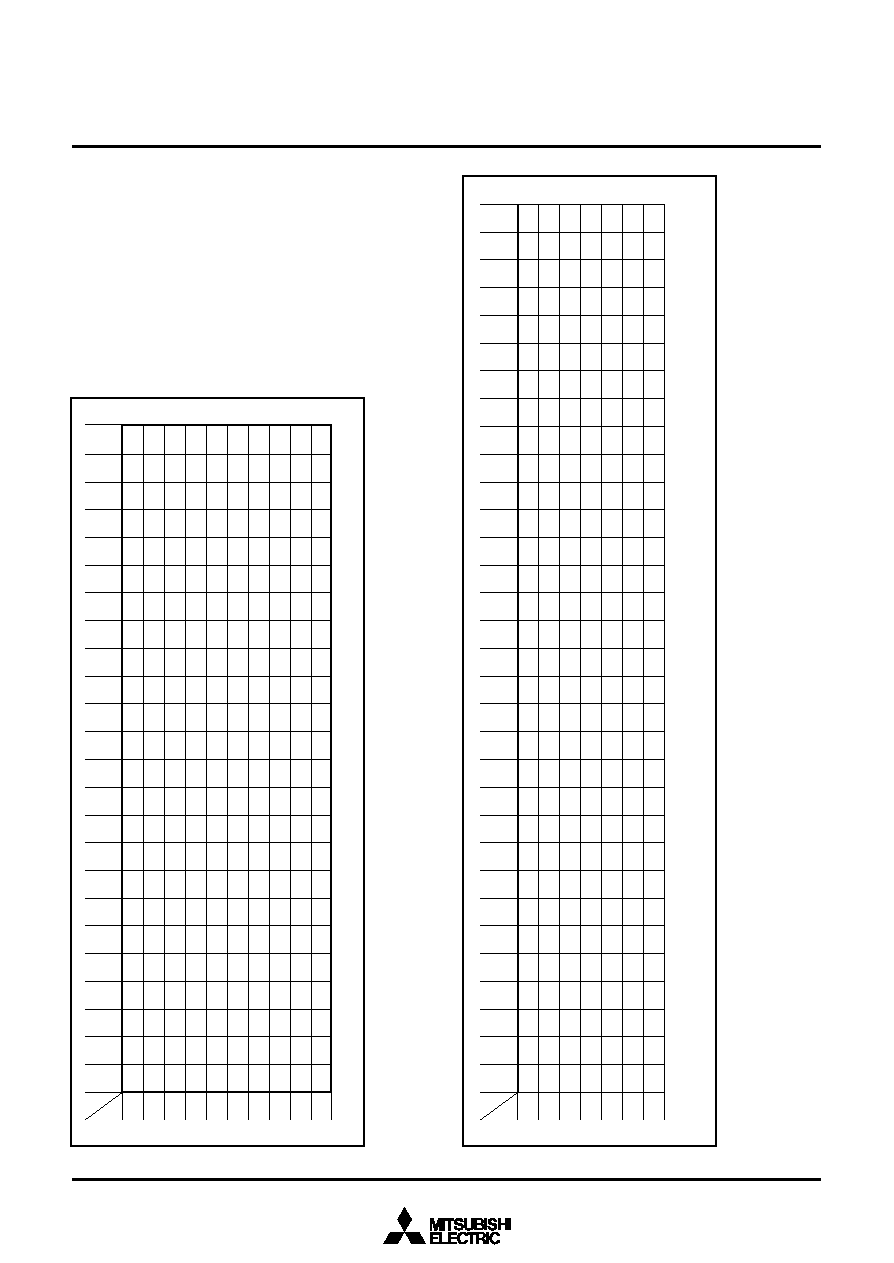
SCREEN CONSTITUTION
The screen lines and rows are determined from each address of the
display RAM. The screen consitution (24 characters
!
10 lines) is
shown in Figure 2 the screen constitution (32 characters
!
7 lines) is
shown in 3.
Note :
The hexadecimal numbers in the boxes show the display RAM address.
1
2
3
4
5
6
7
8
9
10
1
00
16
18
16
30
16
48
16
60
16
78
16
90
16
A8
16
C0
16
D8
16
2
01
16
19
16
31
16
49
16
61
16
79
16
91
16
A9
16
C1
16
D9
16
3
02
16
1A
16
32
16
4A
16
62
16
7A
16
92
16
AA
16
C2
16
DA
16
4
03
16
1B
16
33
16
4B
16
63
16
7B
16
93
16
AB
16
C3
16
DB
16
5
04
16
1C
16
34
16
4C
16
64
16
7C
16
94
16
AC
16
C4
16
DC
16
6
05
16
1D
16
35
16
4D
16
65
16
7D
16
95
16
AD
16
C5
16
DD
16
7
06
16
1E
16
36
16
4E
16
66
16
7E
16
96
16
AE
16
C6
16
DE
16
8
07
16
1F
16
37
16
4F
16
67
16
7F
16
97
16
AF
16
C7
16
DF
16
9
08
16
20
16
38
16
50
16
68
16
80
16
98
16
B0
16
C8
16
E0
16
10
09
16
21
16
39
16
51
16
69
16
81
16
99
16
B1
16
C9
16
E1
16
11
0A
16
22
16
3A
16
52
16
6A
16
82
16
9A
16
B2
16
CA
16
E2
16
12
0B
16
23
16
3B
16
53
16
6B
16
83
16
9B
16
B3
16
CB
16
E3
16
13
0C
16
24
16
3C
16
54
16
6C
16
84
16
9C
16
B4
16
CC
16
E4
16
14
0D
16
25
16
3D
16
55
16
6D
16
85
16
9D
16
B5
16
CD
16
E5
16
15
0E
16
26
16
3E
16
56
16
6E
16
86
16
9E
16
B6
16
CE
16
E6
16
16
0F
16
27
16
3F
16
57
16
6F
16
87
16
9F
16
B7
16
CF
16
E7
16
17
10
16
28
16
40
16
58
16
70
16
88
16
A0
16
B8
16
D0
16
E8
16
18
11
16
29
16
41
16
59
16
71
16
89
16
A1
16
B9
16
D1
16
E9
16
19
12
16
2A
16
42
16
5A
16
72
16
8A
16
A2
16
BA
16
D2
16
EA
16
20
13
16
2B
16
43
16
5B
16
73
16
8B
16
A3
16
BB
16
D3
16
EB
16
21
14
16
2C
16
44
16
5C
16
74
16
8C
16
A4
16
BC
16
D4
16
EC
16
22
15
16
2D
16
45
16
5D
16
75
16
8D
16
A5
16
BD
16
D5
16
ED
16
23
16
16
2E
16
46
16
5E
16
76
16
8E
16
A6
16
BE
16
D6
16
EE
16
24
17
16
2F
16
47
16
5F
16
77
16
8F
16
A7
16
BF
16
D7
16
EF
16
1
2
3
4
5
6
7
1
00
16
20
16
40
16
60
16
80
16
A0
16
C0
16
2
01
16
21
16
41
16
61
16
81
16
A1
16
C1
16
3
02
16
22
16
42
16
62
16
82
16
A2
16
C2
16
4
03
16
23
16
43
16
63
16
83
16
A3
16
C3
16
5
04
16
24
16
44
16
64
16
84
16
A4
16
C4
16
6
05
16
25
16
45
16
65
16
85
16
A5
16
C5
16
7
06
16
26
16
46
16
66
16
86
16
A6
16
C6
16
8
07
16
27
16
47
16
67
16
87
16
A7
16
C7
16
9
08
16
28
16
48
16
68
16
88
16
A8
16
C8
16
10
09
16
29
16
49
16
69
16
89
16
A9
16
C9
16
11
0A
16
2A
16
4A
16
6A
16
8A
16
AA
16
CA
16
12
0B
16
2B
16
4B
16
6B
16
8B
16
AB
16
CB
16
13
0C
16
2C
16
4C
16
6C
16
8C
16
AC
16
CC
16
14
0D
16
2D
16
4D
16
6D
16
8D
16
AD
16
CD
16
15
0E
16
2E
16
4E
16
6E
16
8E
16
AE
16
CE
16
16
0F
16
2F
16
4F
16
6F
16
8F
16
AF
16
CF
16
17
10
16
30
16
50
16
70
16
90
16
B0
16
D0
16
18
11
16
31
16
51
16
71
16
91
16
B1
16
D1
16
19
12
16
32
16
52
16
72
16
92
16
B2
16
D2
16
20
13
16
33
16
53
16
73
16
93
16
B3
16
D3
16
21
14
16
34
16
54
16
74
16
94
16
B4
16
D4
16
22
15
16
35
16
55
16
75
16
95
16
B5
16
D5
16
23
16
16
36
16
56
16
76
16
96
16
B6
16
D6
16
24
17
16
37
16
57
16
77
16
97
16
B7
16
D7
16
25
18
16
38
16
58
16
78
16
98
16
B8
16
D8
16
26
19
16
39
16
59
16
79
16
99
16
B9
16
D9
16
27
1A
16
3A
16
5A
16
7A
16
9A
16
BA
16
DA
16
28
1B
16
3B
16
5B
16
7B
16
9B
16
BB
16
DB
16
29
1C
16
3C
16
5C
16
7C
16
9C
16
BC
16
DC
16
30
1D
16
3D
16
5D
16
7D
16
9D
16
BD
16
DD
16
31
1E
16
3E
16
5E
16
7E
16
9E
16
BE
16
DE
16
32
1F
16
3F
16
5F
16
7F
16
9F
16
BF
16
DF
16
Notes 1.
The hexadecimal numbers in the boxes show the display RAM address.
Notes
2.
When 32 characters
◊
7 lines are displayed, set blank code "FF
16
" to character code of addresses E0
16
to EF
16
.
Fig. 3 Screen constitution (32 characters
!
7 lines)
Fig. 2 Screen constitution (24 characters
!
10 lines)
Rows
Rows
Lines
Lines