Document Outline
- e35071.pdf
- DESCRIPTION
- FEATURES
- APPLICATION
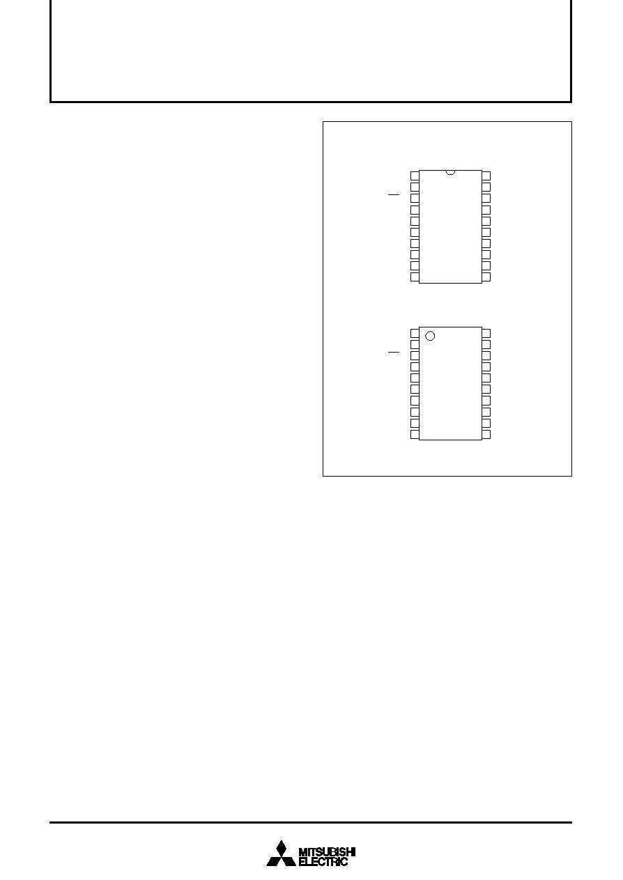
- PIN CONFIGURATION (TOP VIEW)
- PIN DESCRIPTION
- BLOCK DIAGRAM
- MEMORY CONSTITUTION
- SCREEN CONSTITUTION
- DISPLAY RAM
- REGISTERS DESCRIPTION
- REGISTER SUPPLEMENTARY DESCRIPTION
- DISPLAY FORM 1
- DISPLAY FORM 2
- CHARACTER FONT
- DATA INPUT EXAMPLE
- DATA INPUT
- TIMING REQUIREMENTS
- ABSOLUTE MAXIMUM RATINGS
- RECOMMENDED OPERATING CONDITIONS
- ELECTRICAL CHARACTERISTICS
- NOTE FOR SUPPLYING POWER
- PRECAUTION FOR USE
- DATA REQUIRED FOR MASK ROM ORDERING
- STANDARD ROM TYPE : M35071-002SP/FP
- MASK ROM ORDER CONFIRMATION FORM
- 20P4B MARK SPECIFICATION FORM
- 20P2Q-A MARK SPECIFICATION FORM
- PACKAGE OUTLINE
- REVISION DESCRIPTION LIST
DESCRIPTION
The M35071-XXXSP/FP is a character pattern display control IC can
display on the CRT display the liquid crystal display and the plasma
display. It can display 2 pages (24 characters
◊
12 lines per 1 page)
at the same time. It uses a silicon gate CMOS process and it housed
in a 20-pin shrink DIP package (M35071-XXXSP) or a 20-pin shrink
SOP package (M35071-XXXFP).
For M35071-002SP/FP that is a standard ROM version of M35071-
XXXSP/FP respectively, the character pattern is also mentioned.
FEATURES
∑
Screen composition ................ 24 characters
◊
12 lines
◊
2 pages
∑
Number of characters displayed .................. 288 (Max.)
◊
2 pages
∑
Character composition ..................................... 12
◊
18 dot matrix
∑
Characters available ................................ page 0 : 256 characters
page 1 : 128 characters
∑
Character sizes available ................... 4 (vertic al)
◊
2 (horizontal)
∑
Display locations available
Horizontal direction .............................................. 2007 locations
Vertical direction .................................................. 1023 locations
∑
Blinking .................................................................. Character units
Cycle : division of vertical synchronization signal into 32 or 64
Duty
: 25%, 50%, or 75%
∑
Data input ............................. By the I
2
C-BUS serial input function
∑
Coloring
Character color ..................................................... Character unit
Background coloring ............................................. Character unit
Border (shadow) coloring ........................ 8 colors (RGB output)
Specified by register
Raster coloring ........................................ 8 colors (RGB output)
Specified by register
∑
Blanking
Character size blanking
Border size blanking
Matrix-outline blanking
All blanking (all raster area)
∑
Output ports
4 shared output ports (toggled between RGB output)
4 dedicated output ports
∑
Display RAM erase function
∑
Display input frequency range ............... F
OSC
= 20MHz to 90MHz
∑
Horizontal synchronous input frequency
........................................................ H.sync = 15 kHz to 130 kHz
∑
Display oscillation stop function
APPLICATION
CRT display, Liquid crystal display, Plasma display
Outline 20P4B
PIN CONFIGURATION (TOP VIEW)
Outline 20P2Q-A
MITSUBISHI MICROCOMPUTERS
M35071-XXXSP/FP
SCREEN CHARACTER and PATTERN DISPLAY CONTROLLERS
1
2
3
4
5
6
7
8
9
10
20
19
18
17
16
15
14
13
12
11
CPOUT
V
DD2
VERT
HOR
P5/B
P4
P3/G
P2
P1/R
P0/BLNK0
V
SS1
V
SS2
AC
TEST
SCL
SDA
TCK
V
DD1
P6
P7
M35071 - XXXSP
1
2
3
4
5
6
7
8
9
10
20
19
18
17
16
15
14
13
12
11
CPOUT
V
DD2
VERT
HOR
P5/B
P4
P3/G
P2
P1/R
P0/BLNK0
V
SS1
V
SS2
AC
TEST
SCL
SDA
TCK
V
DD1
P6
P7
M35071 - XXXFP
REV.1.1
MITSUBISHI MICROCOMPUTERS
M35071-XXXSP/FP
SCREEN CHARACTER and PATTERN DISPLAY CONTROLLERS
2
Symbol
CPOUT
V
SS2
__
AC
TEST
SCL
SDA
TCK
V
DD1
P6
P7
V
SS1
P0/BLNK0
P1/R
P2
P3/G
P4
P5/B
HOR
VERT
V
DD2
Input/
Output
Output
≠
Input
Input
Input
I/O
Input
≠
Output
Output
≠
Output
Output
Output
Output
Output
Output
Input
Input
≠
Function
Filter output. Connect loop filter to this pin.
Connect to GND.
When "L", this pin resets the internal IC circuit. Hysteresis input. Built-in pull-up resistor.
Test pin. Connect to +5V.
SDA pin serial data is taken in when SCL rises. Hysteresis input.
This is the pin for serial input of display control register and display RAM data. Also, this
pin output acknowledge signal. Hysteresis input. Nch opendrain output.
This is the pin for external clock input.
Please connect to +5V with the power pin.
This is the output port.
This is the output port.
Please connect to GND using circuit earthing pin.
This pin can be toggled between port pin output and BLNK0 signal output.
This pin can be toggled between port pin output and R signal output.
This is the output port.
This pin can be toggled between port pin output and G signal output.
This is the output port.
This pin can be toggled between port pin output and B signal output.
This pin inputs the horizontal synchronous signal. Hysteresis input.
This pin inputs the vertical synchronous signal. Hysteresis input.
Please connect to +5V with the power pin.
Pin name
Filter output
Earthing pin
Auto-clear input
Test input
Clock input
Data I/O
External clock
Power pin
Port P6 output
Port P7 output
Earthing pin
Port P0 output
Port P1 output
Port P2 output
Port P3 output
Port P4 output
Port P5 output
Horizontal synchro-
nous signal input
Vertical synchro-
nous signal input
Power pin
Pin
Number
1
2
3
4
5
6
7
8
9
10
11
12
13
14
15
16
17
18
19
20
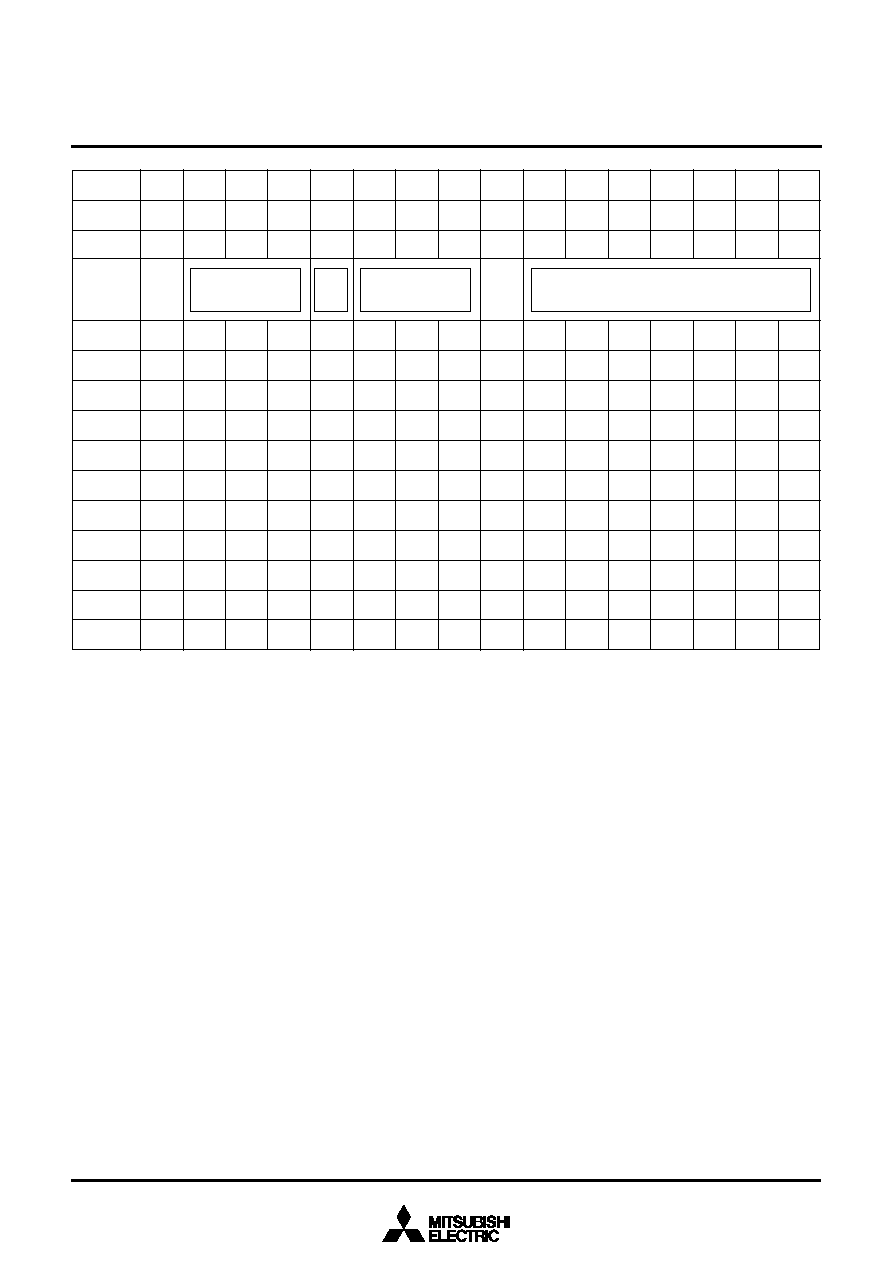
PIN DESCRIPTION
MITSUBISHI MICROCOMPUTERS
M35071-XXXSP/FP
SCREEN CHARACTER and PATTERN DISPLAY CONTROLLERS
3
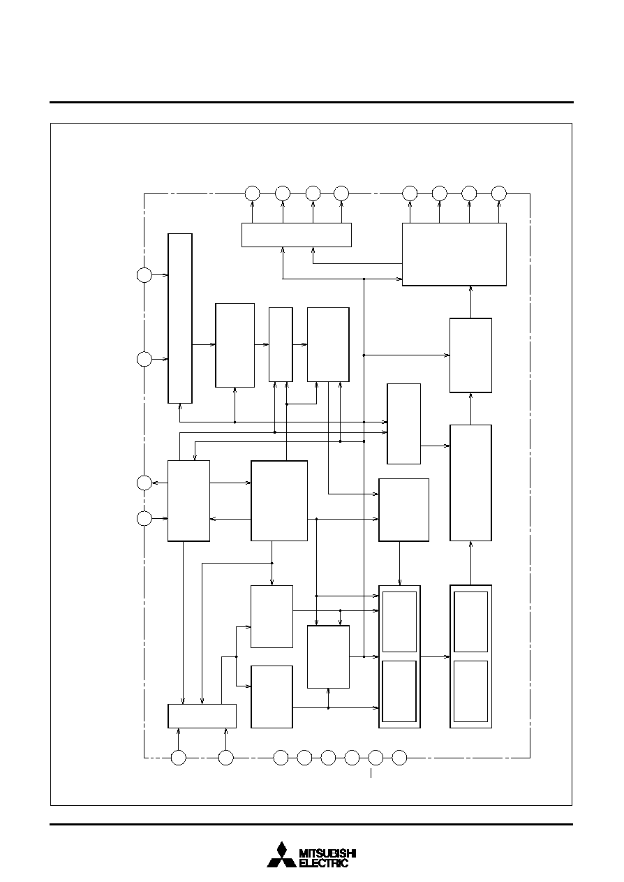
BLOCK DIAGRAM
5
7
6
8
20
4
SCL
SD
A
V
DD1
V
DD2
3
AC
11
V
SS1
2
V
SS2
TEST
Cloc
k oscillation
circuit displa
y
Timing gener
ator
P
olar
ity s
witching circuit
Address control
circuit
Data control
circuit
Displa
y control
register
Displa
y RAM 0
(page 0)
Displa
y RAM 1
(page 1)
Shift register
Blinking circuit
Reading address
control circuit
Displa
y location
detection circuit
H counter
TCK
1
CPOUT
18
HOR
19
12
VER
T
Synchronous signal
s
witching circuit
Displa
y control
circuit
P
o
r
t
output
control circuit
P0/BLNK0
13
P1/R
15
P3/G
17
P5/B
14
P2
16
P4
9P
6
10
P7
Input control circuit
Polarity switching circuit
Displa
y char
acter
R
OM 0
(page 0)
Displa
y char
acter
R
OM 1
(page 1)
MITSUBISHI MICROCOMPUTERS
M35071-XXXSP/FP
SCREEN CHARACTER and PATTERN DISPLAY CONTROLLERS
4
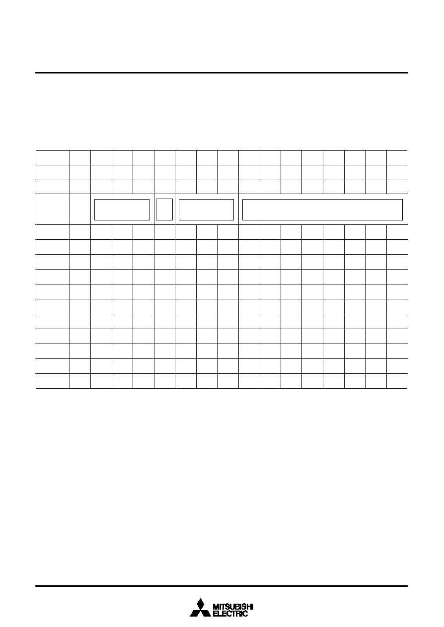
MEMORY CONSTITUTION
Address 000
16
to 11F
16
are assigned to the display RAM, address
120
16
to 128
16
are assigned to the display control registers. The in-
ternal circuit is reset and all display control registers (address 120
16
__
to 128
16
) are set to "0" when the AC pin level is "L". And then, RAM
is not erased and be undefinited. This memory is consisted of 2
Fig. 1
Memory constitution (page 0 memory)
pages : page 0 memory and page 1 memory (their addresses are
common), page controlled by DAF bit of each address when writing
data. For detail, see "Data input". Memory constitution is shown in
Figure 1 and 2.
.........
.........
DAF
DAE
DAD
DAC
DAB
DAA
DA9
DA8
DA7
DA6
DA5
DA4
DA3
DA2
DA1
DA0
0
BB
BG
BR
BLINK
B
G
R
C7
C6
C5
C4
C3
C2
C1
C0
0
BB
BG
BR
BLINK
B
G
R
C7
C6
C5
C4
C3
C2
C1
C0
0
BB
BG
BR
BLINK
B
G
R
C7
C6
C5
C4
C3
C2
C1
C0
0
BB
BG
BR
BLINK
B
G
R
C7
C6
C5
C4
C3
C2
C1
C0
0
EXCK0
VJT
DIVS1 DIVS0 DIV10
DIV9
DIV8
DIV7
DIV6
DIV5
DIV4
DIV3
DIV2
DIV1
DIV0
0
RSEL0 PTD7
PTD6
PTD5
PTD4
PTD3
PTD2
PTD1
PTD0
PTC5
PTC4
PTC3
PTC2
PTC1
PTC0
0
RSEL1 SPACE2 SPACE1 SPACE0 HP10
HP9
HP8
HP7
HP6
HP5
HP4
HP3
HP2
HP1
HP0
0
EXCK1 TEST3 TEST2 TEST1 TEST0
VP9
VP8
VP7
VP6
VP5
VP4
VP3
VP2
VP1
VP0
0
TEST9 TEST5 TEST4 DSP11 DSP10 DSP9
DSP8
DSP7
DSP6
DSP5
DSP4
DSP3
DSP2
DSP1
DSP0
0
TEST10 VSZ1H1 VSZ1H0 VSZ1L1 VSZ1L0 V1SZ1 V1SZ0
LIN9
LIN8
LIN7
LIN6
LIN5
LIN4
LIN3
LIN2
0
POPUP VSZ2H1 VSZ2H0 VSZ2L1 VSZ2L0 V18SZ1 V18SZ0 LIN17 LIN16 LIN15 LIN14 LIN13 LIN12 LIN11 LIN10
0
MODE0 TEST12 HSZ20 TEST11 HSZ10 BETA14 TEST8 TEST7 TEST6
FB
FG
FR
RB
RG
RR
0
MODE1 BLINK2 BLINK1 BLINK0 DSPON STOP RAMERS SYAD
BLK1
BLK0
POLH POLV VMASK
B/F
BCOL
000
16
001
16
11E
16
11F
16
120
16
121
16
122
16
123
16
124
16
125
16
126
16
127
16
128
16
Addresses
Character color
Character code
Background
coloring
Blink-
ing
MITSUBISHI MICROCOMPUTERS
M35071-XXXSP/FP
SCREEN CHARACTER and PATTERN DISPLAY CONTROLLERS
5
DAF
DAE
DAD
DAC
DAB
DAA
DA9
DA8
DA7
DA6
DA5
DA4
DA3
DA2
DA1
DA0
1
BB
BG
BR
BLINK
B
G
R
0
C6
C5
C4
C3
C2
C1
C0
1
BB
BG
BR
BLINK
B
G
R
0
C6
C5
C4
C3
C2
C1
C0
1
BB
BG
BR
BLINK
B
G
R
0
C6
C5
C4
C3
C2
C1
C0
1
BB
BG
BR
BLINK
B
G
R
0
C6
C5
C4
C3
C2
C1
C0
1
≠
≠
≠
≠
≠
≠
≠
≠
≠
≠
≠
≠
≠
≠
≠
1
≠
≠
≠
≠
≠
≠
≠
≠
≠
≠
≠
≠
≠
≠
≠
1
≠
SPACE2 SPACE1 SPACE0 HP10
HP9
HP8
HP7
HP6
HP5
HP4
HP3
HP2
HP1
HP0
1
≠
TEST3 TEST2 TEST1 TEST0
VP9
VP8
VP7
VP6
VP5
VP4
VP3
VP2
VP1
VP0
1
≠
≠
TEST4 DSP11 DSP10 DSP9
DSP8
DSP7
DSP6
DSP5
DSP4
DSP3
DSP2
DSP1
DSP0
1
≠
VSZ1H1 VSZ1H0 VSZ1L1 VSZ1L0 V1SZ1 V1SZ0
LIN9
LIN8
LIN7
LIN6
LIN5
LIN4
LIN3
LIN2
1
≠
VSZ2H1 VSZ2H0 VSZ2L1 VSZ2L0 V18SZ1 V18SZ0 LIN17 LIN16 LIN15 LIN14 LIN13 LIN12 LIN11 LIN10
1
≠
TEST12 HSZ20 TEST11 HSZ10 BETA14 TEST8 TEST7 TEST6
FB
FG
FR
RB
RG
RR
1
≠
BLINK2 BLINK1 BLINK0 DSPON TEST13 RAMERS SYAD
BLK1
BLK0
≠
≠
≠
≠
BCOL
000
16
001
16
11E
16
11F
16
120
16
121
16
122
16
123
16
124
16
125
16
126
16
127
16
128
16
.........
.........
Addresses
Fig. 2
Memory constitution (page 1 memory)
.........
Note: Page 0 and page 1 registers are found in their respective pages. For example, HP10 to HP0 of the page 0 memory sets the horizontal
display start position of page 0, whereas HP10 to HP0 (same register name) of the page 1 memory sets the horizontal display start
position of page 1. Also, registers common to both page 0 and page 1 are found only in the page 0 memory. For example, PTC0 is the
control register of the P0 pin and is found only in the page 0 memory.
Character color
Character code
Background
coloring
Blink-
ing