Äîêóìåíòàöèÿ è îïèñàíèÿ www.docs.chipfind.ru
26
27
25
28
24
29
23
30
22
31
21
32
20
33
19
34
18
35
17
36
16
37
15
38
14
39
13
40
12
41
11
42
10
43
9
44
8
45
7
46
6
47
5
48
4
49
3
50
2
51
1
52
M37210M3-XXXSP
M37210M4-XXXSP
M37211M2-XXXSP
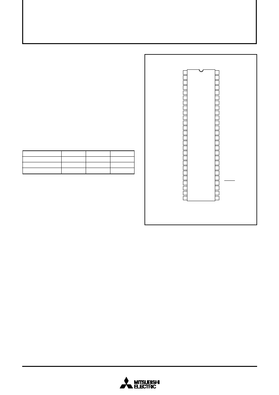
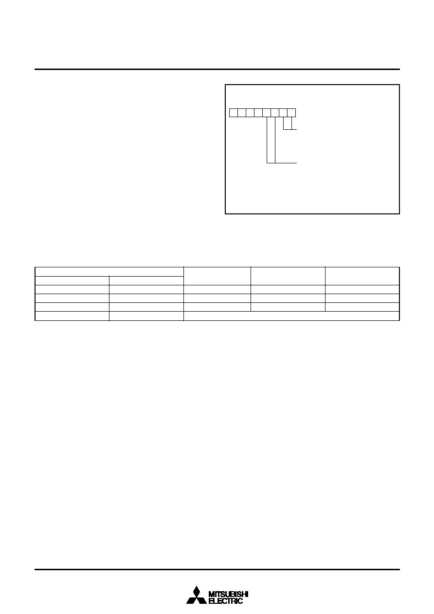
PIN CONFIGURATION (TOP VIEW)
P5
2
/R
P5
3
/G
P5
4
/B
P5
5
/OUT
P2
0
P2
1
P2
2
P2
3
P0
4
P0
5
P0
6
P0
7
P1
0
P1
1
P1
2
P1
3
P1
4
P1
5
/A-D1
P1
6
/A-D2
P1
7
/A-D3
P3
0
P3
1
RESET
OSC1
OSC2
V
CC
Outline 52P4B
DESCRIPTION
The M37210M3-XXXSP/FP is a single-chip microcomputer designed
with CMOS silicon gate technology. It is housed in a 52-pin shrink
plastic molded DIP or a 64-pin plastic molded QFP. This single-chip
microcomputer is useful for the channel selection system for TVs
because it provides PWM function, OSD display function and so on.
In addition to their simple instruction sets, the ROM, RAM, and I/O
addresses are placed on the same memory map to enable easy pro-
gramming.
The features of the M37210E4-XXXSP/FP and the M37210E4SP/FP
are similar to those of the M37210M4-XXXSP except that these
chips have a built-in PROM which can be written electrically.
The differences between the M37210M3-XXXSP/FP, the M37210
M4-XXXSP, and the M37211M2-XXXSP are the ROM size, the RAM
size, and the PWM outputs as shown below. Accordingly, the follow-
ing descriptions will be for the M37210M3-XXXSP/FP unless other-
wise noted.
Note : After the reset, set the stack page selection bit which is set "1"
to "0" because the internal RAM of the M37211M2-XXXSP is
in only the zero page.
FEATURES
·
Number of basic instructions ..................................................... 69
·
Memory size ROM ................ 12 K bytes (M37210M3-XXXSP/FP)
16 K bytes (M37210M4-XXXSP)
8 K bytes (M37211M2-XXXSP)
RAM ................. 256 bytes (M37210M3-XXXSP/FP)
320 bytes (M37210M4-XXXSP)
192 bytes (M37211M2-XXXSP)
ROM for display......................................... 3 K bytes
RAM for display .......................................... 72 bytes
·
The minimum instruction execution time
........................................... 0.5
µ
s (at 8MHz oscillation frequency)
·
Power source voltage ..................................................... 5V ± 10%
·
Power dissipation .............................................................. 110mW
(at 4MHz oscillation frequency, V
CC
= 5.5V, at CRT display)
·
Subroutine nesting ............................................... 96 levels (Max.)
·
Interrupts ....................................................... 12 types, 12 vectors
·
8-bit timers .................................................................................. 4
·
Programmable I/O ports
(Ports P0, P1, P2, P3, P4) ......................................................... 25
·
Output ports (ports P5, P6) .......................................................... 8
·
Output ports (ports P5
2
, P5
6
) ..................................................... 12
·
12 V withstand ports .................................................................... 4
·
Serial I/O ............................................................ 8-bit
!
1 channel
·
PWM output circuit ............... (14-bit
!
1, 6-bit
!
8) ... M37210M3
M37210M4
(14-bit
!
1, 6-bit
!
6) .... M37211M2
Type name
M37210M3-XXXSP/FP
M37210M4-XXXSP
M37211M2-XXXSP
ROM size
12 K bytes
16 K bytes
8 K bytes
RAM size
256 bytes
320 bytes
192 bytes
6-bit PWM outputs
8
8
6
Note : The M37211M2-XXXSP does not have the PWM6 and the PWM7.
·
A-D comparator (5-bit resolution) ................................ 5 channels
·
CRT display function
Display characters ..................................... 18 characters
!
2 lines
(16 lines max.)
Character kinds ................................................................ 96 kinds
Dot structure ............................................................. 12
!
16 dots
Character size .................................................................... 3 kinds
Character color kinds (It can be specified by the character)
max. 7 kinds (R, G, B)
Raster color (max. 7 kinds)
Display layout
Horizontal ..................................................................... 64 levels
Vertical ....................................................................... 128 levels
Bordering (horizontal and vertical)
APPLICATION
TV
MITSUBISHI MICROCOMPUTERS
M37210M3-XXXSP/FP, M37210M4-XXXSP, M37211M2-XXXSP
M37210E4-XXXSP/FP, M37210E4SP/FP
SINGLE-CHIP 8-BIT CMOS MICROCOMPUTER for VOLTAGE SYNTHESIZER
with ON-SCREEN DISPLAY CONTROLLER
H
SYNC
V
SYNC
P6
0
/PWM0
P6
1
/PWM1
P6
2
/PWM2
P6
3
/PWM3
P0
0
/PWM4
P0
1
/PWM5
P0
2
/PWM6
P0
3
/PWM7
P4
2
/S
IN
/A-D5
P4
1
/S
CLK
P4
0
/S
OUT
(/
IN
)
D-A
P3
5
/INT2/A-D4
P3
4
/INT1
P3
3
/TIM3
P3
2
/TIM2
P2
4
P2
5
P2
6
P2
7
CNV
SS
X
IN
X
OUT
V
SS
1
MITSUBISHI MICROCOMPUTERS
M37210M3-XXXSP/FP, M37210M4-XXXSP, M37211M2-XXXSP
M37210E4-XXXSP/FP, M37210E4SP/FP
SINGLE-CHIP 8-BIT CMOS MICROCOMPUTER for VOLTAGE SYNTHESIZER
with ON-SCREEN DISPLAY CONTROLLER
2
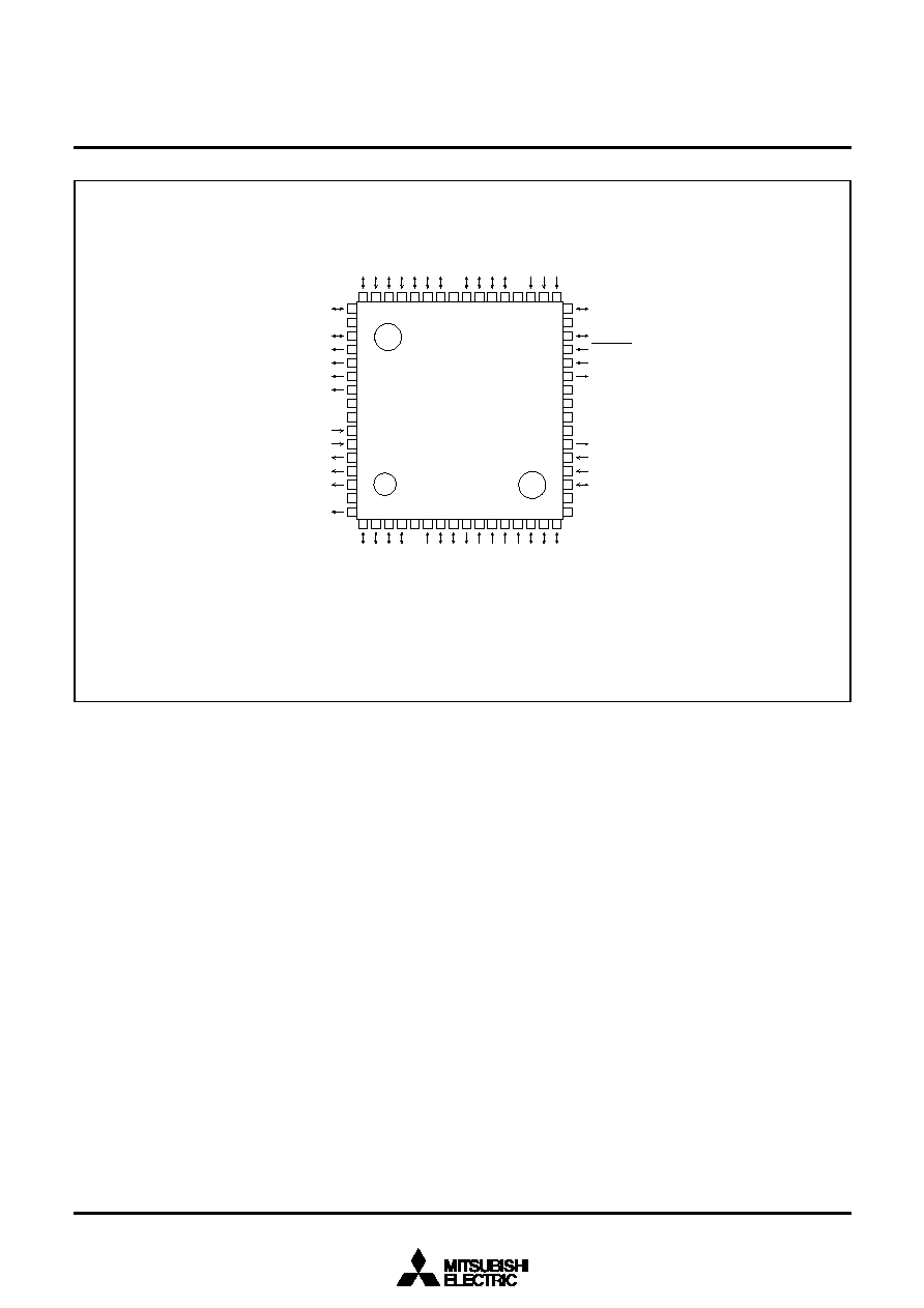
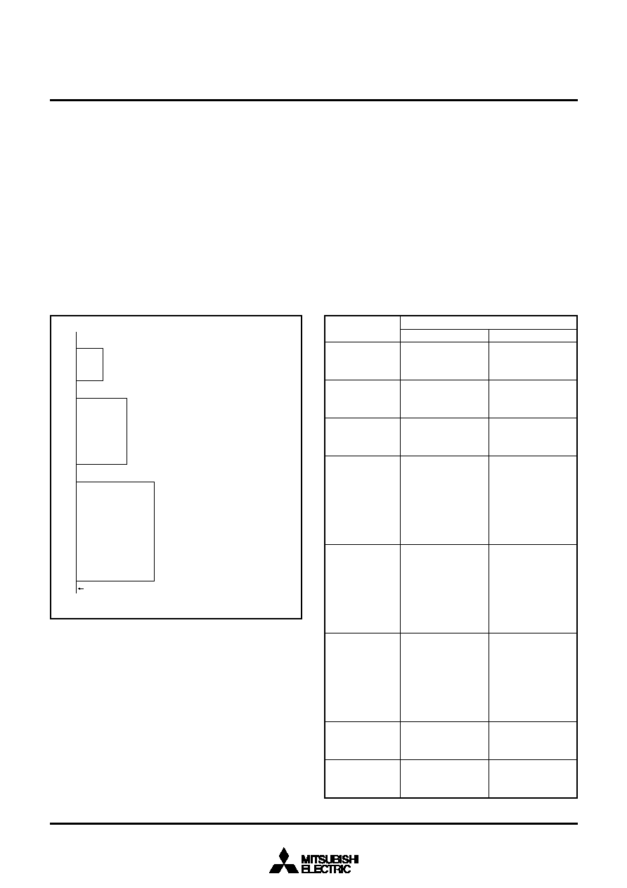
Outline 64P6N-A
NC : No connection
PIN CONFIGURATION (TOP VIEW)
49
50
51
52
53
54
55
56
57
58
59
60
61
62
63
64
32
31
30
29
28
27
26
25
24
23
22
21
20
19
18
17
M37210M3-XXXFP
P3
0
NC
P3
1
RESET
OSC1
OSC2
Vcc
NC
NC
V
SS
X
OUT
X
IN
CNV
SS
P2
7
NC
NC
P2
1
NC
P2
0
P5
5
/OUT
P5
4
/B
P5
3
/G
P5
2
/R
NC
NC
H
SYNC
V
SYNC
P6
0
/PWM0
P6
1
/PWM1
P6
2
/PWM2
NC
P6
3
/PWM3
P2
2
P2
3
P0
4
P0
5
P0
6
P0
7
P1
0
NC
P1
1
P1
2
P1
3
P1
4
NC
P1
5
/A-D1
P1
6
/A-D2
P1
7
/A-D3
P0
0
/
PWM4
P0
1
/
PWM5
P0
2
/
PWM6
P0
3
/
PWM7
NC
P4
2
/S
IN
/A-D5
P4
1
/S
CLK
P4
0
/S
OUT
/(/
IN
)
D-A
P3
5
/
INT2/
A-D4
P3
4
/INT1
P3
3
/TIM3
P3
2
/TIM2
P2
4
P2
5
P2
6
48
47
46
45
44
43
42
41
40
39
38
37
36
35
34
33
1
2
3
4
5
6
7
8
9
10
11
12
13
14
15
16
MITSUBISHI MICROCOMPUTERS
M37210M3-XXXSP/FP, M37210M4-XXXSP, M37211M2-XXXSP
M37210E4-XXXSP/FP, M37210E4SP/FP
SINGLE-CHIP 8-BIT CMOS MICROCOMPUTER for VOLTAGE SYNTHESIZER
with ON-SCREEN DISPLAY CONTROLLER
3
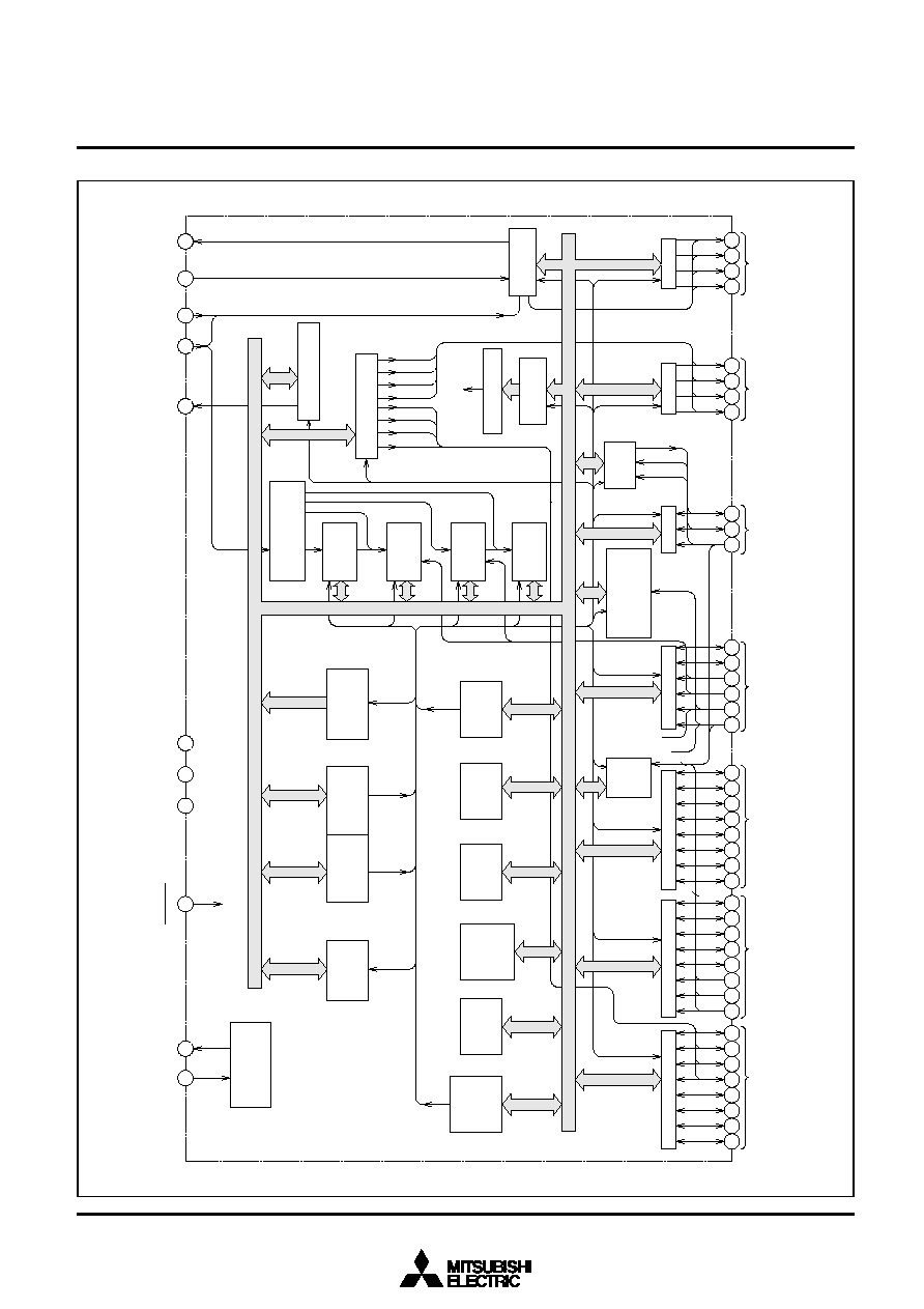
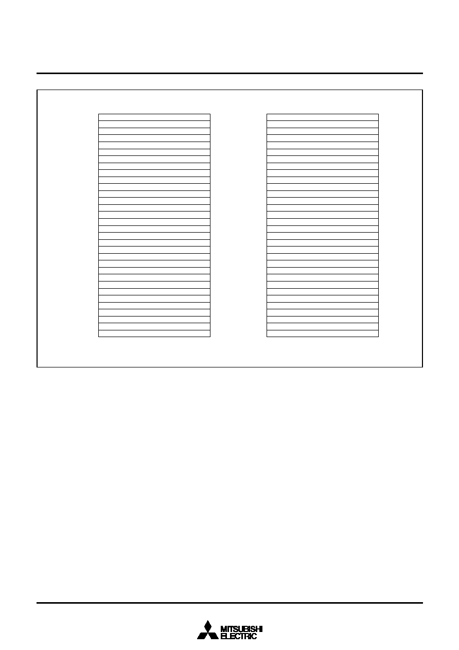
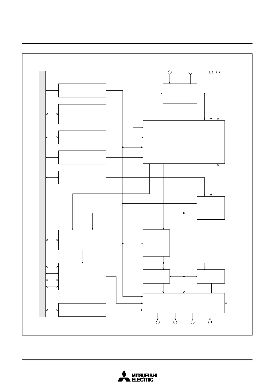
FUNCTIONAL BLOCK DIA
GRAM of M37210M3-XXXSP
Notes 1 : The M37211M2-XXXSP does not have PWM outputs of pi
ns 9 and 10.
2 : 320 bytes for M37210M4-XXXSP and 192 bytes for M37211M2-
XXXSP
3 : 16 K bytes for M37210M4-XXXSP and 8 K bytes for M37211M2
-XXXSP
Clock
input
Clock
output
Reset input
RESET
24
25
30
27
26
23
(5V)
(0V)
(0V)
V
CC
V
SS
CNV
SS
D-A
14
H
SYNC
12
Y
SYNC
OSC1
OSC2
29
28
14-bit PWM circuit
6-bit PWM circuit
Instruction decoder
Control signal
Instruction
register
CRT circuit
PWM7
PWM6
PWM5
PWM4
PWM3
PWM2
PWM1
PWM0
Timer count
source selection
circuit
Timer 1
T1 (8)
Timer 2
T2 (8)
Timer 3
T3 (8)
Timer 4
T4 (8)
TIM2
TIM3
Interrupt interval
determination
circuit
SI/O(8)
P4(3)
S
IN
S
CLK
S
OUT
P6(4)
P3(6)
P5(4)
OUT
B
G
R
A-D5
INT1, INT2
INT1
INT2
A-D4
P2(8)
P1(8)
P0(8)
A-D1
A-D2
A-D3
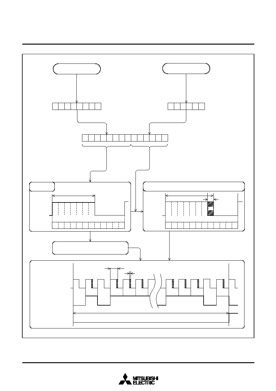
3
5
4
1
4
2
4
3
4
4
1
0
9
8
7
3
3
3
4
3
5
3
6
3
73
8
3
9
4
0
2
22
1
2
0
1
9
4
5
4
6
4
7
4
8
1
51
6
1
7
1
83
1
3
2
1
11
2
1
3
6
5
4
3
4
9
5
05
15
2
I
/O port P0
I
/O port P1
I
/O port P2
I
/O port P3
I
/O port P4
Output port P6
Video signal output
A-D
compa-
rator
Stack
pointer
(8)
Index
register Y
(8)
Accumulator
A(8)
8-bit
arithmetic
and logical
unit
RAM
256bytes
(Note 2)
Program
counter
PC
H
(8)
Program
counter
PC
L
(8)
ROM
12 K bytes
(Note 3)
Clock
generating
circuit
Address bus
Data bus
X
IN
X
OUT
Index
register X
(8)
Processor
status
register
PS(8)
MITSUBISHI MICROCOMPUTERS
M37210M3-XXXSP/FP, M37210M4-XXXSP, M37211M2-XXXSP
M37210E4-XXXSP/FP, M37210E4SP/FP
SINGLE-CHIP 8-BIT CMOS MICROCOMPUTER for VOLTAGE SYNTHESIZER
with ON-SCREEN DISPLAY CONTROLLER
4
M37210M3-XXXSP, M37210M4-XXXSP, M37211M2-XXXSP
M37210M3-XXXFP
Number of character
Character dot construction
Kinds of characters
Character size
Kinds of color
Display position (horizontal, vertical)
FUNCTIONS
Parameter
M37210M3-XXXSP/FP
M37210M4-XXXSP
M37211M2-XXXSP
P0
P1
0
P1
4
P1
5
P1
7
P2
P3
0
, P3
1
P3
2
, P3
5
P4
0
, P4
1
P4
2
P5
P6
at CRT display ON
at CRT display OFF
at stop mode
ROM
RAM
ROM
RAM
ROM
RAM
I/O
I/O
Input
I/O
I/O
Input
I/O
Input
Output
Output
Functions
69
0.5
µ
s (the minimum instruction execution time, at 8MHz oscillation frequency)
8MHz
12 K bytes
256 bytes
16 K bytes
320 bytes
8 K bytes
192 bytes
8-bit
!
1 (can be used as N-channel open-drain output and PWM4-PWM7)(Note)
5-bit
!
1 (CMOS 3-state output)
3-bit
!
1 (can be used as A-D input)
8-bit
!
1 (CMOS 3-state output)
2-bit
!
1 (CMOS 3-state input/output)
4-bit
!
1 (can be used as timer input pins, INT input pins and A-D input pins)
2-bit
!
1 (can be used as N-channel open-drain output and serial I/O function pins)
1-bit
!
1 (can be used as serial I/O and A-D input)
4-bit
!
1 (can be used as R, G, B, OUT pins)
4-bit
!
1 (can be used as N-channel open-drain output and PWM0-PWM3 output pins)
8-bit
!
1
8-bit timer
!
4
96 levels (max.)
Two external interrupts, four internal timer interrupts,
one serial I/O interrupt, one CRT interrupt, one f(X
IN
)/4096
interrupt, one V
SYNC
interrupt, BRK instruction
Built-in circuit (externally connected a ceramic resonator or a quartz-crystal oscillator)
5V ± 10%
110mW (at 4MHz oscillation frequency, V
CC
= 5.5V, Typ.)
55mW (at 4MHz oscillation frequency, V
CC
= 5.5V, Typ.)
1.65mW (Max.)
-
10 to 70°C
CMOS silicon gate process
52-pin shrink plastic molded DIP
64-pin plastic molded QFP
18 characters
!
2 lines : maximum 16 lines (by software)
12
!
16 dots
96 kinds
3 kinds
7 kinds max, (R, G, B) : can be specified by character unit
64 levels (horizontal)
!
128 levels (vertical)
Number of basic instructions
Instruction execution time
Clock frequency
Memory size
Input/Output ports
Serial I/O
Timers
Subroutine nesting
Interrupt
Clock generating circuit
Power source voltage
Power dissipation
Operating temperature range
Device structure
Package
CRT display function
Note : The M37211M2-XXXSP can be also used as PWM4 and PWM5.
MITSUBISHI MICROCOMPUTERS
M37210M3-XXXSP/FP, M37210M4-XXXSP, M37211M2-XXXSP
M37210E4-XXXSP/FP, M37210E4SP/FP
SINGLE-CHIP 8-BIT CMOS MICROCOMPUTER for VOLTAGE SYNTHESIZER
with ON-SCREEN DISPLAY CONTROLLER
5
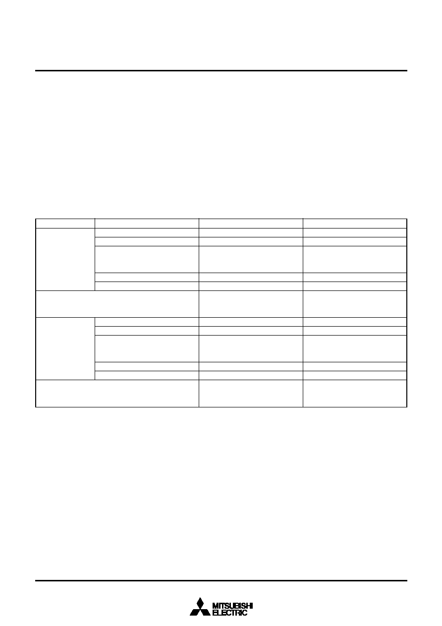
PIN DESCRIPTION
Pin
V
CC
,
V
SS
CNV
SS
RESET
X
IN
X
OUT
P0
0
P0
7
P1
1
P1
4
P1
5
P1
7
P2
0
P2
7
P3
0
, P3
1
P3
2
P3
5
P4
0
, P4
1
P4
2
P6
0
P6
3
OSC1,
OSC2
H
SYNC
V
SYNC
R, G, B,
OUT
D-A
Name
Power source voltage
CNV
SS
Reset input
Clock input
Clock output
Timing output
I/O port P0
I/O port P1
Input port P1
I/O port P2
I/O port P3
Input port P3
I/O port P4
Input port P4
Output port P6
Clock input for CRT
display
Clock output for CRT
display
H
SYNC
input
V
SYNC
input
CRT output
DA Output
Input /
Output
Input
Input
Output
Output
I/O
I/O
Input
I/O
I/O
Input
I/O
Input
Output
Input
Output
Input
Input
Output
Output
Functions
Apply voltage of 5V ± 10% to V
CC
, and 0V to V
SS
.
This is connected to V
SS
.
To enter the reset state, the reset input pin must be kept at a "L" for 2
µ
s or more (under nor-
mal V
CC
conditions).
If more time is needed for the crystal oscillator to stabilize, this "L" condition should be main-
tained for the required time.
This chip has an internal clock generating circuit. To control generating frequency, an exter-
nal ceramic resonator or a quartz-crystal oscillator is connected between the X
IN
and
X
OUT
pins. If an external clock is used, the clock source should be connected the X
IN
pin and
the X
OUT
pin should be left open.
This is the timing output pin.
Port P0 is an 8-bit I/O port with directional registers allowing each I/O bit to be individually
programmed as input or output. At reset, this port is set to input mode. The output structure
is CMOS output.
The output structure is N-channel open-drain output. When PWM4, PWM5, PWM6 and
PWM7 are used, P0
0
, P0
1
, P0
2
and P0
3
are in common with PWM output pins of PWM4,
PWM5, PWM6 and PWM7.
Ports P1
0
, P1
1
, P1
2
, P1
3
and P1
4
are 5-bit I/O ports and have basically the same functions
as port P0. The output structure is CMOS output.
Ports P1
5
, P1
6
and P1
7
are 3-bit input ports and they are in common with input pins of A-D
comparator (A-D1, A-D2 and A-D3).
Port P2 is an 8-bit I/O port and has basically the same functions as port P0.
The output structure is CMOS output.
Ports P3
0
and P3
1
are 2-bit I/O ports and have basically the same functions as port P0.
The output structure is CMOS output.
Ports P3
2
, P3
3
, P3
4
and P3
5
are 4-bit input ports and ports P3
2
and P3
3
are in common
with external clock input pins of timers 2 and 3. Ports P3
4
and P3
5
are in common with
external interrupt input pins INT1 and INT2. Port P3
5
is in common with an input pin of A-D
comparator (A-D4).
Ports P4
0
and P4
1
are 2-bit I/O ports and have basically the same functions as port P0.
When serial I/O is used, ports P4
0
and P4
1
are in common with S
OUT
pin and S
CLK
pin, re-
spectively.
Port P4
2
is an 1-bit Input port, and it is common with an input pin of A-D comparator (A-D5)
and serial input pin (S
IN
).
Port P6 is an 4-bit output port. The output structure is N-channel open-drain. This port is in
common with 6-bit PWM output pins PWM0-PWM3.
This is the I/O pins of the clock generating circuit for the CRT display function.
This is the horizontal synchronizing signal input for CRT display.
This is the vertical synchronizing signal input for CRT display.
This is a 4-bit output pin for CRT display. The output structure is CMOS output. This is in
common with port P5
2
P5
5
.
This is an output pin for 14-bit PWM.
MITSUBISHI MICROCOMPUTERS
M37210M3-XXXSP/FP, M37210M4-XXXSP, M37211M2-XXXSP
M37210E4-XXXSP/FP, M37210E4SP/FP
SINGLE-CHIP 8-BIT CMOS MICROCOMPUTER for VOLTAGE SYNTHESIZER
with ON-SCREEN DISPLAY CONTROLLER
6
FUNCTIONAL DESCRIPTION
Central Processing Unit (CPU)
The M37210M3-XXXSP/FP uses the standard 740 family instruction
set. Refer to the table of 740 family addressing modes and machine
instructions or the SERIES 740
Software
User's Manual for details
on the instruction set.
Machine-resident 740 family instructions are as follows :
The FST and SLW instruction cannot be used.
The MUL, DIV, WIT, and STP instruction can be used.
CPU Mode Register
The CPU mode register is allocated at address 00FB
16
. The CPU
mode register contains the stack page selection bit.
Note : Please beware of this bit when programming because it is set to "1" after the reset release.
Especially the internal RAM of the M37211M2-XXXSP is in the zero page, so be sure to set this bit to "0".
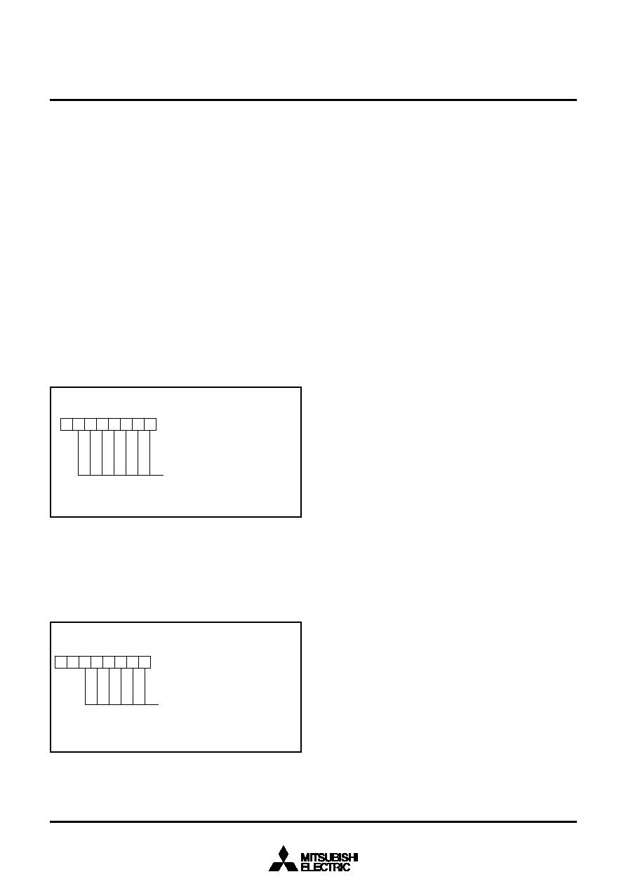
Fig. 1 Structure of CPU mode register
7
0
Fix these bits to "00
2
"
CPU mode register
(CPUM : address 00FB
16
)
Stack page selection bit (Note)
0 : Zero page
1 : 1 page
Fix these bits to "1111
2
"
0
0
1
1
1
1
1
MITSUBISHI MICROCOMPUTERS
M37210M3-XXXSP/FP, M37210M4-XXXSP, M37211M2-XXXSP
M37210E4-XXXSP/FP, M37210E4SP/FP
SINGLE-CHIP 8-BIT CMOS MICROCOMPUTER for VOLTAGE SYNTHESIZER
with ON-SCREEN DISPLAY CONTROLLER
7
Fig. 2 Memory map
MEMORY
Special Function Register (SFR) Area
The special function register (SFR) area in the zero page contains
control registers such as I/O ports and timers.
RAM
RAM is used for data storage and for stack area of subroutine calls
and interrupts.
ROM
ROM is used for sroring user programs as well as the interrupt vec-
tor area.
RAM for Display
RAM for display is used for specifing the character codes and colors
to display.
ROM for Display
ROM for display is used for storing character data.
Interrupt Vector Area
The interrupt vector area contains reset and interrupt vectors.
Zero Page
The 256 bytes from addresses 0000
16
to 00FF
16
are called the zero
page area. The internal RAM and the special function registers
(SFR) are allocated to this area.
The zero page addressing mode can be used to specify memory and
register addresses in the zero page area. Access to this area with
only 2 bytes is possible in the zero page addressing mode.
Special Page
The 256 bytes from addresses FF00
16
to FFFF
16
are called the spe-
cial page area. The special page addressing mode can be used to
specify memory addresses in the special page area. Access to this
area with only 2 bytes is possible in the special page addressing
mode.
0000
16
00BF
16
00FF
16
013F
16
017F
16
2000
16
20B1
16
3000
16
35FF
16
3800
16
3DFF
16
FFDE
16
FF00
16
RAM
(192 bytes)
for
M37211M2
RAM
(256 bytes)
for
M37210M3
ROM for display
(3 K bytes)
ROM
(8 K bytes)
for
M37211M2
Zero page
Special page
SFR area
Not used
Not used
Not used
Not used
Interrupt vector area
C000
16
D000
16
E000
16
FFFF
16
RAM for display (Note)
(72 bytes)
RAM
(320 bytes)
for
M37210M4
ROM
(12 K bytes)
for
M37210M3
ROM
(16 K bytes)
for
M37210M4
Note : Refer to Table 6. Contents of CRT display RAM
MITSUBISHI MICROCOMPUTERS
M37210M3-XXXSP/FP, M37210M4-XXXSP, M37211M2-XXXSP
M37210E4-XXXSP/FP, M37210E4SP/FP
SINGLE-CHIP 8-BIT CMOS MICROCOMPUTER for VOLTAGE SYNTHESIZER
with ON-SCREEN DISPLAY CONTROLLER
8
Fig. 3 Memory map of special function register (SFR )
Note : The M37211M2-XXXSP dose not have this register
00C1
16
00C0
16
00C2
16
00C3
16
00C4
16
00C5
16
00C6
16
00C7
16
00C8
16
00C9
16
00CA
16
00CB
16
00CC
16
00CD
16
00CE
16
00CF
16
00D0
16
00D1
16
00D2
16
00D3
16
00D4
16
00D5
16
00D6
16
00D7
16
00D8
16
00D9
16
00DA
16
00DB
16
00DC
16
00DD
16
00DE
16
00DF
16
Port P1
Port P2
Port P3
Port P4
Port P5
Port P5 control register
Port P6
Port P6 directional register
14DA-H register
14DA-L register
PWM1 register
PWM0 register
PWM3 register
PWM4 register
PWM output control register 1
PWM output control register 2
Interrupt Interval determination register
Interrupt Interval determination control register
Serial I/O mode register
Serial I/O register
Port P0
Port P0 directional register
Port P1 directional register
Port P2 directional register
Port P3 directional register
Port P4 directional register
PWM2 register
Vertical position register 2 (block 2)
Character size register
Color register 0
Color register 2
CRT control register
CRT port control register
A-D mode register
A-D control register
Timer 2
Timer 1
Timer 4
Timer 34 mode register
PWM5 register
PWM6 register (Note)
PWM7 register (Note)
CPU mode register
Interrupt request register 1
Interrupt request register 2
Interrupt control register1
Interrupt control register2
Horizontal position register
Vertical position register 1 (block 1)
Border selection register
Color register 1
Color register 3
Timer 3
Timer 12 mode register
00E0
16
00E1
16
00E2
16
00E3
16
00E4
16
00E5
16
00E6
16
00E7
16
00E8
16
00E9
16
00EA
16
00EB
16
00EC
16
00ED
16
00EE
16
00EF
16
00F0
16
00F1
16
00F2
16
00F3
16
00F4
16
00F5
16
00F6
16
00F7
16
00F8
16
00F9
16
00FA
16
00FB
16
00FC
16
00FD
16
00FE
16
00FF
16
MITSUBISHI MICROCOMPUTERS
M37210M3-XXXSP/FP, M37210M4-XXXSP, M37211M2-XXXSP
M37210E4-XXXSP/FP, M37210E4SP/FP
SINGLE-CHIP 8-BIT CMOS MICROCOMPUTER for VOLTAGE SYNTHESIZER
with ON-SCREEN DISPLAY CONTROLLER
9
Table 1. Interrupt vector addresses and priority
Interrupt sources
Reset
CRT interrupt
INT
2
interrupt
INT
1
interrupt
Timer 4 interrupt
f(X
IN
)/4096 interrupt
V
SYNC
interrupt
Timer 3 interrupt
Timer 2 interrupt
Timer 1 interrupt
Serial I/O interrupt
BRK instruction interrupt
Remarks
Non-maskable
Active edge selectable
Active edge selectable
Active edge selectable
Non-maskable software interrupt
INTERRUPTS
Interrupts can be caused by 12 different sources consisting of 3 ex-
ternal, 7 internal, 1 software, and reset.
Interrupts are vectored interrupts with priorities shown in Table 1. Re-
set is also included in the table because its operation is similar to an
interrupt.
When an interrupt is accepted, the registers are pushed, interrupt
disable flag I is set, and the program jumps to the address specified
in the vector table. The interrupt request bit is cleared automatically.
The reset can never be disabled. Other interrupts are disabled when
the interrupt disable flag is set.
Priority
1
2
3
4
5
6
7
8
9
10
11
12
Vector addresses
FFFF
16
, FFFE
16
FFFD
16
, FFFC
16
FFFB
16
, FFFA
16
FFF9
16
, FFF8
16
FFF5
16
, FFF4
16
FFF3
16
, FFF2
16
FFF1
16
, FFF0
16
FFEF
16
, FFEE
16
FFED
16
, FFEC
16
FFEB
16
, FFEA
16
FFE9
16
, FFE8
16
FFDF
16
, FFDE
16
All interrupts except the BRK instruction interrupt have an interrupt
request bit and an interrupt enable bit. The interrupt request bits are
in interrupt request registers 1 and 2 and the interrupt enable bits are
in interrupt control registers 1 and 2. Figure 4 shows the structure of
the interrupt request registers 1 and 2 and interrupt control registers
1 and 2.
Interrupts other than the BRK instruction interrupt and reset are ac-
cepted when the interrupt enable bit is "1", interrupt request bit is "1",
and the interrupt disable flag is "0". The interrupt request bit can be
reset with a program, but not set. The interrupt enable bit can be set
and reset with a program.
Reset is treated as a non-maskable interrupt with the highest priority.
Figure 5 shows interrupts control.
MITSUBISHI MICROCOMPUTERS
M37210M3-XXXSP/FP, M37210M4-XXXSP, M37211M2-XXXSP
M37210E4-XXXSP/FP, M37210E4SP/FP
SINGLE-CHIP 8-BIT CMOS MICROCOMPUTER for VOLTAGE SYNTHESIZER
with ON-SCREEN DISPLAY CONTROLLER
10
Fig. 5 Interrupt control
Fig. 4 Structure of interrupt-related registers
Interrupt request bit
Interrupt enable bit
Interrupt disable flag (I)
BRK instruction
reset
interrupt request
INT
1
interrupt enable bit
INT
2
interrupt enable bit
Serial I/O1 interrupt enable bit
Fix this bit to "0"
f(X
IN
)/4096 interrupt enable bit
Fix these bits to "0"
7
0
Timer 1 interrupt request bit
Timer 2 interrupt request bit
Timer 3 interrupt request bit
Timer 4 interrupt request bit
CRT interrupt request bit
V
SYNC
interrupt request bit
Interrupt request register 1
(IREQ1 : address 00FC
16
)
7
0
INT
1
interrupt request bit
INT
2
interrupt request bit
Serial I/O1 interrupt request bit
f(X
IN
)/4096 interrupt request bit
Fix this bit to "0"
Interrupt request register 2
(IREQ2 : address 00FD
16
)
7
0
Timer 1 interrupt enable bit
Timer 2 interrupt enable bit
Timer 3 interrupt enable bit
Timer 4 interrupt enable bit
CRT interrupt enable bit
V
SYNC
interrupt enable bit
Fix these bits to "0"
Interrupt control register 1
(ICON1 : address 00FE
16
)
7
0
Interrupt control register 2
(ICON2 : address 00FF
16
)
0 : No interrupt request issued
1 : Interrupt request issued
0 : Interrupt disabled
1 : Interrupt enabled
0
0 0 0
0 0
MITSUBISHI MICROCOMPUTERS
M37210M3-XXXSP/FP, M37210M4-XXXSP, M37211M2-XXXSP
M37210E4-XXXSP/FP, M37210E4SP/FP
SINGLE-CHIP 8-BIT CMOS MICROCOMPUTER for VOLTAGE SYNTHESIZER
with ON-SCREEN DISPLAY CONTROLLER
11
Fig. 6 Structure of timer-related registers
TIMERS
The M37210M3-XXXSP has 4 timers: timer 1, timer 2, timer 3 and
timer 4. All timers are 8-bit timers with the 8-bit timer latch. The timer
block diagram is shown in Figure 7.
All of the timers count down and their divide ratio is 1/(n+1), where n
is the value of timer latch. The value is set to a timer at the same time
by writing a count value to the corresponding timer latch (addresses
00F0
16
to 00F3
16
: timers 1 to 4).
The count value is decremented by 1. The timer interrupt request bit
is set to "1" by an timer overflow at the next count pulse after the
count value reaches "00
16.
"
(1) Timer 1
Timer 1 can select one of the following count sources:
·
f(X
IN
)/16
·
f(X
IN
)/4096
The count source of timer 1 is selected by setting bit 0 of the timer 12
mode register (address 00F4
16
).
Timer 1 interrupt request occurs at timer 1 overflow.
(2) Timer 2
Timer 2 can select one of the following count sources:
·
f(X
IN
)/16
·
Timer 1 overflow signal
·
External clock from the P3
2
/TIM2 pin
The count source of timer 2 is selected by setting bits 4 and 1 of the
timer 12 mode register (address 00F4
16
). When timer 1 overflow
signal is a count source for the timer 2, the timer 1 functions as an 8-
bit prescaler.
Timer 2 interrupt request occurs at timer 2 overflow.
(3) Timer 3
Timer 3 can select one of the following count sources:
·
f(X
IN
)/16
·
External clock from the P3
3
/TIM3 pin and the H
SYNC
pin
The count source of timer 3 is selected by setting bits 5 and 0 of the
timer 34 mode register (address 00F5
16
).
Timer 3 interrupt request occurs at timer 3 overflow.
(4) Timer 4
Timer 4 can select one of the following count sources:
·
f(X
IN
)/16
·
f(X
IN
)/2
·
Timer 3 overflow signal
The count source of timer 3 is selected by setting bits 4 and 1 of the
timer 34 mode register 2 (address 00F5
16
). When timer 3 overflow
signal is a count source for the timer 4, the timer 3 functions as an 8-
bit prescaler.
Timer 4 interrupt request occurs at timer 4 overflow.
At reset, timers 3 and 4 are connected by hardware and "FF
16
" is
automatically set in timer 3; "07
16
" in timer 4. The f(X
IN
)/16 is se-
lected as the timer 3 count source. The internal reset is released by
timer 4 overflow at these state, the internal clock is connected .
At execution of the STP instruction, timers 3 and 4 are connected by
hardware and "FF
16
" is automatically set in timer 3; "07
16
" in timer 4.
However, the f(X
IN
)16 is not selected as the timer 3 count source. So
set bit 0 of the timer 34 mode register (address 00F5
16
) to "0" before
the execution of the STP instruction (f(X
IN
)16 is selected as the timer
3 count source). The internal STP state is released by timer 4 over-
flow at these state, the internal clock is connected .
Because of this, the program starts with stable clock.
The structure of timer-related registers is shown in Figure 6.
Timer 2 internal count source
selection bit
0 : f (X
IN
) /16
1 : Timer 1 overflow signal
Timer 2 count stop bit
0 : Operation
1 : stop
Timer 1 count stop bit
0 : Operation
1 : Stop
Timer 2 count source selection bit
0 : Internal clock source
1 : External clock source from P3
2
/TIM2 pin
Timer 1 count source selection bit
0 : f (X
IN
) /16
1 : 1024
µ
s
clock
Timer 12 mode register
(TM12MR : address 00F4
16
)
7
0
Timer 3 count source selection bit
0 : f (X
IN
) /16
1 : External clock source (bits)
Timer 34 mode register
(TM34MR : address 00F5
16
)
Timer 4 internal count source
selection bit
0 : Timer 3 overflow signal
1 : f (X
IN
) /16
Timer 3 count stop bit
0 : Operation
1 : Stop
Timer 4 count stop bit
0 : Operation
1 : Stop
Timer 4 count source selection bit
0 : Internal clock source
1 : f (X
IN
) /2
7
0
Timer 3 external count source
selection bit
0 : P3
3
/TIM3 pin input
1 : H
SYNC
pin input
Fix this bit to "0"
MITSUBISHI MICROCOMPUTERS
M37210M3-XXXSP/FP, M37210M4-XXXSP, M37211M2-XXXSP
M37210E4-XXXSP/FP, M37210E4SP/FP
SINGLE-CHIP 8-BIT CMOS MICROCOMPUTER for VOLTAGE SYNTHESIZER
with ON-SCREEN DISPLAY CONTROLLER
12
Fig. 7 Timer block diagram
Notes 1 : "H" pulse width of external clock inputs TIM2 and TIM3 needs 4 machine cycles or more.
2 : When the external clock source is selected, timers 2 and 3 are counted at a rising edge of input signal.
3 : In the stop mode or the wait mode, external clock inputs TIM2 and TIM3 cannot be used.
8
8
8
Data bus
X
IN
1/2
1/8
Timer 1 latch (8)
Timer 1 (8)
Timer 2 latch (8)
Timer 2 (8)
8
8
8
D.F.
D.F.
8
8
Timer 3 latch (8)
Timer 3 (8)
T12M
0
T12M
2
T12M
4
T12M
1
T12M
3
T34M
0
T34M
2
T34M
1
Timer 4 latch (8)
Timer 4 (8)
8
P3
2
/TIM2
P3
3
/TIM3
Timer 1
interrupt request
T34M
4
T34M
3
07
16
8
8
8
Timer 2
interrupt request
Timer 3
interrupt request
Reset
STP instruction
Timer 4
interrupt request
FF
16
H
SYNC
T34M
5
Selection gate : Connected to black
colored side at reset.
1/4096
T12M : Timer 12 mode register
T34M : Timer 34 mode register
MITSUBISHI MICROCOMPUTERS
M37210M3-XXXSP/FP, M37210M4-XXXSP, M37211M2-XXXSP
M37210E4-XXXSP/FP, M37210E4SP/FP
SINGLE-CHIP 8-BIT CMOS MICROCOMPUTER for VOLTAGE SYNTHESIZER
with ON-SCREEN DISPLAY CONTROLLER
13
Fig. 8 Serial I/O block diagram
SERIAL I/O
M37210M3-XXXSP has a serial I/O.
A block diagram of the serial I/O is shown in Figure 8.
Synchronous input/output clock (S
CLK
), and the serial I/O pins (S
OUT
,
S
IN
) are used as port P4. The serial I/O mode registers (address
00DC
16
) are 8-bit registers. Bits 0, 1 and 2 of these registers are
used to select a synchronous clock source.
Bit 3 decides whether parts of P4 will be used as a serial I/O or not.
To use P4
2
as a serial input, set the directional register bit which cor-
responds to P4
2
to "0". For more information on the directional regis-
ter, refer to the I/O pin section.
The serial I/O function is discussed below. The function of the serial
I/O differs depending on the clock source ; external clock or internal
clock.
Data bus
X
IN
8
1/2
1/2
P4
1
latch
P4
1
/S
CLK
SM
3
P4
0
latch
SM
3
P4
0
/S
OUT
P4
2
/S
IN
SM
2
SM
1
SM
0
1/4
1/8 1/16
Frequency
divider
Serial I/O counter (8)
SM
5
: LSB
MSB
Serial I/O shift register (8)
(address 00DD
16
)
Serial I/O
interrupt request
Synchronization
circuit
SM
6
Selection gate : Connected to black
colored side at reset.
MITSUBISHI MICROCOMPUTERS
M37210M3-XXXSP/FP, M37210M4-XXXSP, M37211M2-XXXSP
M37210E4-XXXSP/FP, M37210E4SP/FP
SINGLE-CHIP 8-BIT CMOS MICROCOMPUTER for VOLTAGE SYNTHESIZER
with ON-SCREEN DISPLAY CONTROLLER
14
Fig. 9 Serial I/O timing (for LSB first)
The serial I/O counter is set to 7 when data is stored in the serial I/O
register. At each falling edge of the transfer clock, serial data is out-
put to S
OUT
. During the rising edge of this clock, data can be input
from S
IN
and the data in the serial I/O register will be shifted 1 bit.
Transfer direction can be selected by bit 5 of serial I/O mode register.
After the transfer clock has counted 8 times, the serial I/O register will
be empty and the transfer clock will remain at a high level. At this time
the interrupt request bit will be set.
External clock- If an external clock is used, the interrupt request will
be sent after the transfer clock has counted 8 times but transfer clock
will not stop.
Due to this reason, the external clock must be controlled from the
outside. The external clock should not exceed 1MHz at a duty cycle
of 50%. The timing diagram is shown in Figure 9. When using an ex-
ternal clock for transfer, the external clock must be held at "H" level
when the serial I/O counter is initialized. When switching between the
internal clock and external clock, the switching must not be per-
formed during transfer. Also, the serial I/O counter must be initialized
after switching.
Notes 1: On programming, note that the serial I/O counter is set by
writing to the serial I/O register with the bit managing in-
structions as SEB and CLB instructions.
2: When an external clock is used as the synchronizing clock,
write transmit data to the serial I/O register at "H" of the
transfer clock input level.
D
0
D
1
D
2
D
3
D
4
D
5
D
6
D
7
(Note 1)
Interrupt request bit set
Sync. clock
Transfer clock
Serial I/O register
write signal
Serial I/O output
S
OUT
Serial I/O input
S
IN
Notes 1 : If internal clock is selected, the Sout pin is at high impedance after transfer is completed.
2 : When an external clock is used as the synchronous clock, write the transmit data to the
serial I/O shift register at "H" of the transfer clock input level.

MITSUBISHI MICROCOMPUTERS
M37210M3-XXXSP/FP, M37210M4-XXXSP, M37211M2-XXXSP
M37210E4-XXXSP/FP, M37210E4SP/FP
SINGLE-CHIP 8-BIT CMOS MICROCOMPUTER for VOLTAGE SYNTHESIZER
with ON-SCREEN DISPLAY CONTROLLER
15
Fig. 10 Structure of serial I/O mode register
Serial I/O common transmission/reception mode.
Write 1 to bit 6 of serial I/O mode register, and signals S
IN
and S
OUT
switch internal to be able to serial data transmission/reception.
Figure 11 shows signals on serial I/O common transmission/recep-
tion mode.
Note : Receive the serial data after writing "FF
16
" to the serial I/O
register.
Fig. 11 Signals on serial I/O common transmission/reception mode
7
0
Internal synchronous clock
selection bits
00 : f (X
IN
) /4
01 : f (X
IN
) /16
10 : f (X
IN
) /32
11 : f (X
IN
) /64
Serial l/O mode register
(SM : address 00DC
16
)
Synchronous clock selection bit
0 : External clock
1 : Internal clock
Fix this bit to "0"
Serial l/O port selection bit
0 : P4
0,
P4
1
1 : S
OUT1
,S
CLK
signal output pins
Transfer direction selection bit
0 : LSB first
1 : MSB first
Serial input pin selection bit
0 : Input from S
IN
pin
1 : Input from S
OUT
pin
Serial I/O shift register
P4
1
/S
CLK
P4
0
/S
OUT
(
/IN
)
P4
2
/S
IN
clock1
Input or output
The transmission mode
SM
6
Port P4
2
data
"1"
The reception mode
"0"
MITSUBISHI MICROCOMPUTERS
M37210M3-XXXSP/FP, M37210M4-XXXSP, M37211M2-XXXSP
M37210E4-XXXSP/FP, M37210E4SP/FP
SINGLE-CHIP 8-BIT CMOS MICROCOMPUTER for VOLTAGE SYNTHESIZER
with ON-SCREEN DISPLAY CONTROLLER
16
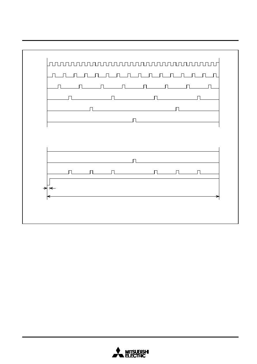
within one period in the circuit internal section. Refer to Figure
13 (a).
Six different pulses can be output from the PWM.
These can be selected by bits 0 through 5. Depending on the
content of the 6-bit PWM latch, pulses from 5 to 0 are selected.
The PWM output is the difference of the sum of each of these
pulses. Several examples are shown in Figure 13 (b). Changes
in the contents of the PWM latch allows the selection of 64
lengths of high-level area outputs varying from 0/64 to 63/64. A
length of entirely high-level output cannot be output, i.e. 64/64.
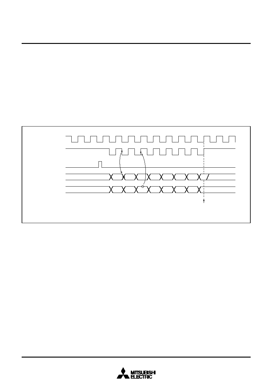
(5) 14-bit PWM Operation
The output example of the 14-bit PWM is shown in Figure 14.
The 14-bit PWM divides the data within the PWM latch into the
lower 6 bits and higher 8 bits.
A high-level area within a length D
H
times
is output every short
area of t = 256
=128
µ
s as determined by data D
H
of the higher
8 bits.
Thus, the time for the high-level area is equal to the time set by
the lower 8 bits or that plus
. As a result, the short-area period
t ( = 128
µ
s, approx. 7.8 kHz) becomes an approximately repeti-
tive period.
(6) Output after Reset
At reset the output of port P6 is in the high impedance state and
the contents of the PWM register and latch are undefined. Note
that after setting the PWM register, its data is transferred to the
latch.
Table 2. Relation between the low-order 6 bits of data and high-level
area increase space
6 low-order bits of data
0 0 0 0 0 0
0 0 0 0 0 1
0 0 0 0 1 0
0 0 0 1 0 0
0 0 1 0 0 0
0 1 0 0 0 0
1 0 0 0 0 0
LSB
Area longer by
than that of other t
m
(m = 0 to 63)
Nothing
m = 32
m = 16, 48
m = 8, 24, 40, 56
m = 4, 12, 20, 28, 36, 44, 52, 60
m = 2, 6, 10, 14, 18, 22, 26, 30, 34, 38, 42, 46, 50, 54, 58, 62
m = 1, 3, 5, 7, ................................................... 57, 59, 61, 63
PWM OUTPUT CIRCUIT
(1) Introduction
The M37210M3-XXXSP/FP and M37210M4-XXXSP are
equipped with one 14-bit PWM (DA) and eight 6-bit PWMs
(PWM0-PWM7), and the M37211M2-XXXSP is equipped with
six 6-bit PWMs (PWM0-PWM5). The 14-bit resolution gives DA
the minimum resolution bit width of 500ns (for f(X
IN
)
= 4MHz)
and a repeat period of 8192
µ
s. PWM0-PWM7 have a 6-bit reso-
lution with minimum resolution bit width of 16
m
s and repeat pe-
riod of 1024
µ
s.
Block diagram of the PWM is shown in Figure 16.
The PWM timing generator section applies individual control
signals to DA and PWM0-7 using clock input X
IN
divided by 2
as a reference signal.
(2) Data Setting
The output pins PWM0-3 are in common with port P6 and
PWM4-7 are in common with port P0
0
-P0
3
.
For PWM output, each PWM output selection bit (bit 1 to 7 of
PWM output control register 1, bit 0, 1 of PWM output control
register 2, should be set. When DA is used for output, first set
the higher 8-bit of the DA-H register (address 00CE
16
), then the
lower 6-bit of the DA-L register (address 00CF
16
).
When one of the PWM0-7 is used for output, set the 6-bit in the
PWM0-7 register (address 00D0
16
to 00D4
16
, 00F6
16
to
00F8
16
), respectively.
(3) Transferring Data from Registers to PWM
Circuit
The data written to the PWM registers. 8 bits of the DA-H regis-
ter is transferred to 14-bit PWM circuit when writing to lower 6
bits of the DA-L register.
(4) Operation of the 6-bit PWMs
The timing diagram of the eight 6-bit PWMs (PWM0-7) is shown
in Figure 13. One period (T) is composed of 64 (2
6
) segments.
There are six different pulse types configured from bits 0 to 5
representing the significance of each bit. These are output
MITSUBISHI MICROCOMPUTERS
M37210M3-XXXSP/FP, M37210M4-XXXSP, M37211M2-XXXSP
M37210E4-XXXSP/FP, M37210E4SP/FP
SINGLE-CHIP 8-BIT CMOS MICROCOMPUTER for VOLTAGE SYNTHESIZER
with ON-SCREEN DISPLAY CONTROLLER
17
Fig. 12 PWM block diagram
Note : The M37211M2-XXXSP can not output the PWM.
PW : PWM output control register 1
PN : PWM output control register 2
D0 : Port P0 direction register
P0 : Port P0
D6 : Port P6 directional register
P6 : Port P6
Inside of is as same contents with the others.
Data bus
PWM0 register
(address 00D0
16
)
8
PN
3
P6
0
D6
0
PW
2
PWM0
Selection gate : connected to black
colored side at reset.
P6
1
D6
1
PW
3
PWM1
P6
2
D6
2
PW
4
PWM2
P6
3
D6
3
PW
5
PWM3
P0
0
D0
0
PW
6
PWM4
P0
1
D0
1
PW
7
PWM5
P0
2
D0
2
PN
0
PWM6(Note)
P0
3
D0
3
PN
1
PWM7(Note)
Timing
generator
for PWM
1/2
PW
0
6-bit PWM circuit
PN
2
14-bit PWM circuit
PN
4
DA
D-A
PW
1
X
IN
bit 5
MSB
LSB
6
8
bit 7
bit 0
bit 0
DA-H register
(address 00CE
16
)
(14-bit)
DA-L register
(address 00CF
16
)
6
14
Pass gate
MITSUBISHI MICROCOMPUTERS
M37210M3-XXXSP/FP, M37210M4-XXXSP, M37211M2-XXXSP
M37210E4-XXXSP/FP, M37210E4SP/FP
SINGLE-CHIP 8-BIT CMOS MICROCOMPUTER for VOLTAGE SYNTHESIZER
with ON-SCREEN DISPLAY CONTROLLER
18
Fig. 13 6-bit PWM timing
2
6
10
14
18
22
26
30
34
38
42
46
50
54
58
62
1
3
5
7
9
19
39
59
8
4
12
20
28
36
44
52
60
Bit 5
Bit 4
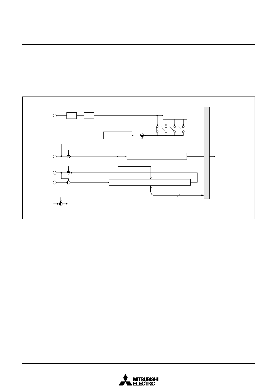
Bit 3
Bit 2
Bit 1
Bit 0
00
16
(0)
01
16
(1)
06
16
(24)
3F
16
(63)
16
48
32
(a) Pulses showing the weight of each bit
T = 64t
PWM output t = 10
µ
s T = 1024
µ
s
f (X
IN
) = 4MHz
(b) Example of 6-bit PWM output
24
40
56
MITSUBISHI MICROCOMPUTERS
M37210M3-XXXSP/FP, M37210M4-XXXSP, M37211M2-XXXSP
M37210E4-XXXSP/FP, M37210E4SP/FP
SINGLE-CHIP 8-BIT CMOS MICROCOMPUTER for VOLTAGE SYNTHESIZER
with ON-SCREEN DISPLAY CONTROLLER
19
Fig. 14 14-bit PWM output example (f (X
IN
) = 4MHz)
Set "2C
16
" to DA-H register
Set "28
16
" to DA-L register
[DA-H register]
[DA latch]
bit 7
These bits decide smaller intervals tm in which "H"
level area
is
["H" level area of fundamental waveform plus r]
These bits decide "H"
level area
of fundamental waveform
Fundamental
waveform
14-bit
8-bit
counter
PWM output
0
0
1
0
1
1
0
0
bit 0
After writing of DA-L
After writing
bit 13
bit 0
0
0
1
0
1
1
0
0
1
0
1
0
0
0
1
0
0
1
0
0
bit 0
Waveform of smaller intervals tm specified by the lower 6 bits
14-bit
PWM output
8-bit
counter
FF FE FD
D6 D5 D4 D3
02 01 00
The fundamental waveform of smaller intervals
tm which is not specified by the lower 6 bits is
not changed
14-bit PWM output
Low-order 6-bit
output of DA latch
t
0
t
1
t
2
t
3
t
4
t
5
t
59
t
60
t
61
t
62
t
63
(
)
"H"
level area of
fundamental waveform
Minimum bit
durations 0.5
µ
s
High-order 8 bit
value of DA latch
=
!
(
) (
0.5
µ
s
!
44
0.5
µ
s
!
45
0.5
µ
s
2C 2B 2A
03 02 01
FF FE FD
D6 D5 D4 D3
02 01 00
2C 2B 2A
03 02 01 00
)
0.5
µ
s
!
45
T = 8192
µ
s
[DA-L register]
00
= 0.5
µ
s
...
...
...
...
...
...
MITSUBISHI MICROCOMPUTERS
M37210M3-XXXSP/FP, M37210M4-XXXSP, M37211M2-XXXSP
M37210E4-XXXSP/FP, M37210E4SP/FP
SINGLE-CHIP 8-BIT CMOS MICROCOMPUTER for VOLTAGE SYNTHESIZER
with ON-SCREEN DISPLAY CONTROLLER
20
Fig.15 Structure of PWM output control registers 1 and 2
Note : Fix this bit to "0" (M37211M2-XXXSP).
PWM output control register 2
(PN : address 00D6
16
)
P0
0
/PWM4 output selection bit
0 : P0
0
(general-purpose) output
1 : PWM4 (6-bit PWM) output
P6
3
/PWM3 output selection bit
0 : P6
3
(general-purpose) output
1 : PWM3 (6-bit PWM) output
P6
2
/PWM2 output selection bit
0 : P6
2
(general-purpose) output
1 : PWM2 (6-bit PWM) output
P6
1
/PWM1 output selection bit
0 : P6
1
(general-purpose) output
1 : PWM1 (6-bit PWM) output
P6
0
/PWM0 output selection bit
0 : P6
0
(general-purpose) output
1 : PWM0 (6-bit PWM) output
D-A pin general-purpose output register
0 : Output "L"
1 : Output "H"
7
0
DA, PWM count source STOP bit
0 : Supply
1 : Stop
PWM output control register 1
(PW : address 00D5
16
)
DA/PN
4
output selection bit
0 : DA (14-bit PWM) output
1 : PN
4
(general-purpose) output
7
0
P0
1
/PWM5 output selection bit
0 : P0
1
(general-purpose) output
1 : PWM5 (6-bit PWM) output
P0
2
/PWM6 output selection bit (Note)
0 : P0
2
(general-purpose) output
1 : PWM6 (6-bit PWM) output
P0
3
/PWM7 output selection bit (Note)
0 : P0
3
(general-purpose) output
1 : PWM7 (6-bit PWM) output
DA output polarity selection bit
0 : Positive polarity
1 : Negative polarity
6-bit PWM output polarity selection bit
0 : Positive polarity
1 : Negative polarity
MITSUBISHI MICROCOMPUTERS
M37210M3-XXXSP/FP, M37210M4-XXXSP, M37211M2-XXXSP
M37210E4-XXXSP/FP, M37210E4SP/FP
SINGLE-CHIP 8-BIT CMOS MICROCOMPUTER for VOLTAGE SYNTHESIZER
with ON-SCREEN DISPLAY CONTROLLER
21
Fig. 18 A-D comparator block diagram
Fig. 17 Structure of A-D mode register
Fig. 16 Structure of A-D control register
Table 3. Relationship between the contents of A-D control register
and reference voltage
A-D control register
Reference voltage Vref
1/64 V
CC
3/64 V
CC
5/64 V
CC
27/64 V
CC
29/64 V
CC
31/64 V
CC
Bit4
0
0
0
1
1
1
Bit 3
0
0
0
1
1
1
Bit 2
0
0
0
1
1
1
Bit 1
0
0
1
0
1
1
Bit 0
0
1
0
1
0
1
........................
........................
........................
........................
........................
........................
7
0
A-D input pin selection bits
0 0 0 : A-D1
0 0 1 : A-D2
0 1 0 : A-D3
0 1 1 : A-D4
1 0 0 : A-D5
A-D mode regiser
(ADM : address 00EE
16
)
1 0 1 :
1 1 0 :
1 1 1 :
These are not
available
A-D mode register
Bits 0 to 2
P1
5
/A-D1
Analog
signal
switch
Comparator
Bit 4
Bit 3
Bit 2
Bit 1
Bit 0
Switch tree
Resistor ladder
A-D control register
Data bus
Bit 5
Comparator control
P1
6
/A-D2
P1
7
/A-D3
P3
5
/A-D4
P4
2
/A-D5
7
0
D-A converter set bits
(refer to table 3)
A-D control register
(ADC : address 00EF
16
)
Strage bit of comparison result
0 : Input voltage <
reference voltage
1 : Input voltage >
reference voltage
A-D COMPARATOR
Block diagram of A-D comparator is shown in Figure 18. A-D com-
parator consists of 5-bit D-A converter and comparator. The A-D con-
trol register can generate 1/64 V
CC
-step internal analog voltage
based on the settings of bits 0 to 4.
Table 3 gives the relation between the descriptions of A-D control
register bits 0 to 4 and the generated internal analog voltage. The
comparison result of the analog input voltage and the internal analog
voltage is stored in the A-D control register, bit 5.
After selection of an analog input pin by bits 0-2 of A-D mode register
(address 00EE
16
), the digital value corresponding to the internal ana-
log voltage to be compared is then written in the A-D control register,
bit 0 to 3 and an analog input pin is selected. After 16 machine cycle,
the voltage comparison is completed.
MITSUBISHI MICROCOMPUTERS
M37210M3-XXXSP/FP, M37210M4-XXXSP, M37211M2-XXXSP
M37210E4-XXXSP/FP, M37210E4SP/FP
SINGLE-CHIP 8-BIT CMOS MICROCOMPUTER for VOLTAGE SYNTHESIZER
with ON-SCREEN DISPLAY CONTROLLER
22
12 dots
16 dots
Functions
18 characters
!
2 lines
12
!
16 dots (refer to Figure 19)
96
3 kinds
1 screen : 4 kinds
A character
Possible (multiline display)
Possible (maximum 7 kinds)
CRT DISPLAY FUNCTIONS
(1) Outline of CRT Display Functions
Table 4 outlines the CRT display functions of the M37210M3-XXXSP.
The M37210M3-XXXSP incorporates a 18 columns
!
2 lines CRT
display control circuit. CRT display is controlled by the CRT display
control register.
Up to 96 kinds of characters can be displayed, and colors can be
specified for each character. Four colors can be displayed on one
screen. A combination of up to 7 colors can be obtained by using
each output signal (R, G and B).
Characters are displayed in a 12
!
16 dot configuration to obtain
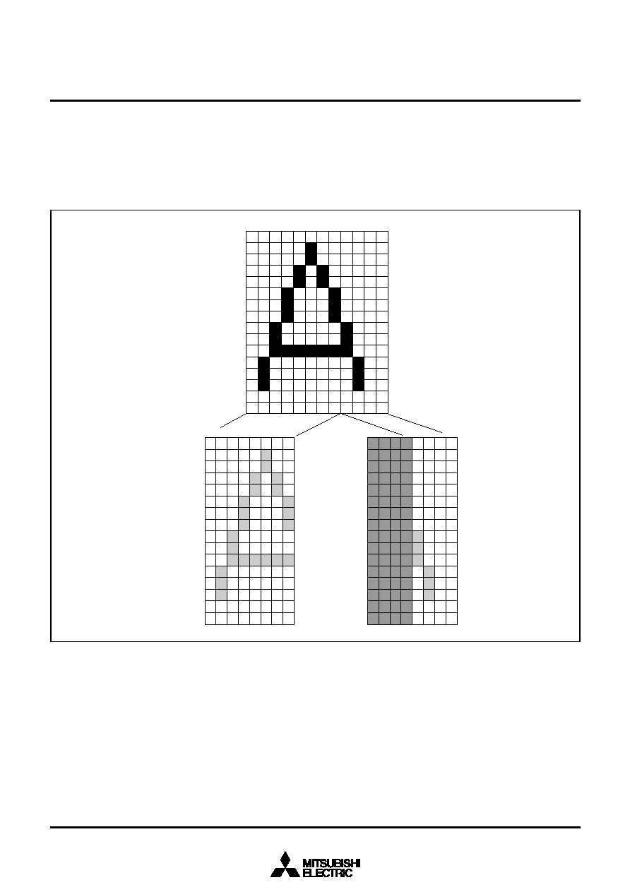
smooth character patterns (refer to Figure 19).
The following shows the procedure how to display characters on the
CRT screen.
Fig. 19 CRT display character configuration
Fig. 20 Structure of CRT control register
Set the character to be displayed in display RAM.
Set the display color by using the color register.
Specify the color register in which the display color is set by us-
ing the display RAM.
Specify the vertical position and character size by using the verti-
cal position register and the character size register.
Specify the horizontal position by using the horizontal position
register.
Write the display enable bit to the designated block display flag of
the CRT control register. When this is done, the CRT starts op-
eration according to the input of the V
SYNC
signal.
The CRT display circuit has an extended display mode.
This mode allows multiple lines (more than 3 lines) to be displayed
on the screen by interrupting the display each time one line is dis-
played and rewriting data in the block for which display is terminated
by software.
Figure 21 shows a block diagram of the CRT display control circuit.
Figure 20 shows the structure of the CRT display control register.
Table 4. Outline of CRT display functions
Parameter
Number of display
character
Character
configuration
Kinds of character
Character size
Color
Display expansion
Raster coloring
Kinds of color
Coloring unit
Note : Display is controlled by logical product (AND) between the all-
blocks display control bit and each block display control bit
7
0
CRT control register
(CC : address 00EA
16
)
Display of all blocks control bit (Note)
0 : Display of all blocks off
1 : Display of all blocks on
Display of block 1 control bit
0 : Display of block 1 off
1 : Display of block 1 on
Display of block 2 control bit
0 : Display of block 2 off
1 : Display of block 2 on
MITSUBISHI MICROCOMPUTERS
M37210M3-XXXSP/FP, M37210M4-XXXSP, M37211M2-XXXSP
M37210E4-XXXSP/FP, M37210E4SP/FP
SINGLE-CHIP 8-BIT CMOS MICROCOMPUTER for VOLTAGE SYNTHESIZER
with ON-SCREEN DISPLAY CONTROLLER
23
Fig. 21 Block diagram of CRT display control circuit
(Address 00EA
16
)
CRT control register
(Addresses 00E1
16
to 00E2
16
)
Vertical position registers
(Address 00E4
16
)
Character size register
(Address 00E0
16
)
Horizontal position register
(Address 00E5
16
)
Border selection register
(Addresses 00E6
16
to 00E9
16
)
Color registers
(Address 00EC
16
)
CRT port control register
Data bus
R
G
B
OUT
Output circuit
Shift register
12 bits
Shift register
12 bits
ROM for display
12 bits
×
16
×
96
Display control
circuit
Display position control circuit
Display oscillation
circuit
OSC1
OSC2
H
SYNC
V
SYNC
RAM for display
9 bits
×
18
×
2
MITSUBISHI MICROCOMPUTERS
M37210M3-XXXSP/FP, M37210M4-XXXSP, M37211M2-XXXSP
M37210E4-XXXSP/FP, M37210E4SP/FP
SINGLE-CHIP 8-BIT CMOS MICROCOMPUTER for VOLTAGE SYNTHESIZER
with ON-SCREEN DISPLAY CONTROLLER
24
Fig. 23 Structure of horizontal position register
(2) Display Position
The display positions of characters are specified in units called a
"block". There are two blocks, block 1 and block 2.
Up to 18 characters can be displayed in one block (refer to (4)
Memory for Display).
The display position of each block in both horizontal and vertical di-
rections can be set by software.
The horizontal direction is common to all blocks, and is selected from
64-step display positions in units of 4Tc (Tc = oscillating cycle for dis-
play).
The display position in the vertical direction is selected from 128-step
display positions for each block in units of four scanning lines.
Block 2 is displayed after the display of block 1 perfectly (fig. 24(a)).
Then if the display of block 2 starts during the display of block 1, only
block 1 is displayed. As same, when multiline display, block 1 is dis-
played after the display of block 2 perfectly (fig. 24(b)).
The vertical position can be specified from 128-step positions (four
scanning lines per step) for each block by setting values 00
16
to 7F
16
to bits 0 to 6 in the vertical position register (addresses 00E1
16
and
00E2
15
). Figure 22 shows the structure of the vertical position regis-
ter.
The horizontal direction is common to all blocks, and can be speci-
fied from 64-step display positions (4Tc per step (Tc = oscillating
cycle for display) by setting values 00
16
to 3F
16
to bits 0 to 5 in the
horizontal position register (address 00E0
16
). Figure 23 shows the
structure of the horizontal position register.
Fig. 22 Structure of vertical position registers
7
0
Vertical position registers 1, 2
(CV1 : address 00E1
16
)
(CV2 : address 00E2
16
)
The vertical display start positions
128-step positions (00
16
to 7F
16
)
7
0
Horizontal position register
(HR : address 00E0
16
)
The horizontal display start positions
64-step positions (00
16
to 3F
16
)
MITSUBISHI MICROCOMPUTERS
M37210M3-XXXSP/FP, M37210M4-XXXSP, M37211M2-XXXSP
M37210E4-XXXSP/FP, M37210E4SP/FP
SINGLE-CHIP 8-BIT CMOS MICROCOMPUTER for VOLTAGE SYNTHESIZER
with ON-SCREEN DISPLAY CONTROLLER
25
Fig. 24 Display position
Block 2
(a) Example when each block is separated
(b) Example when block 2 overlaps with block 1
(RH)
CV
1
CV
2
Block 1
Block 2
CV
1
CV
2
Block 1
Block 1 (second)
CV
1
No display
No display
MITSUBISHI MICROCOMPUTERS
M37210M3-XXXSP/FP, M37210M4-XXXSP, M37211M2-XXXSP
M37210E4-XXXSP/FP, M37210E4SP/FP
SINGLE-CHIP 8-BIT CMOS MICROCOMPUTER for VOLTAGE SYNTHESIZER
with ON-SCREEN DISPLAY CONTROLLER
26
(3) Character Size
The size of characters to be displayed can be selected from three
sizes for each block. Use the character size register (address
00E4
16
) to set a character size. The character size in block 1 can be
specified by using bits 0 and 1 in the character size register ; the
character size in block 2 can be specified by using bits 2 and 3. Fig-
ure 25 shows the structure of the character size register.
The character size can be selected from three sizes : small size, me-
dium size and large size. Each character size is determined by the
number of scanning lines in the height (vertical) direction and the
cycle of display oscillation ( = Tc) in the width (horizontal) direction.
The small size consists of [one scanning line]
!
[1 Tc] ; the medium
size consists of [two scanning lines]
!
[2 Tc] ; and the large size con-
sists of [three scanning lines]
!
[3 Tc].
Table 5 shows the relationship between the set values in the charac-
ter size register and the character sizes.
Table 5. The relationship between the set values of the character size register and the character sizes
Set values of the character size register
CSn
0
0
1
0
1
CSn
1
0
0
1
1
Character
size
Minimum
Medium
Large
Width (horizontal) direction
Tc : oscillating cycle for display
1 Tc
2 Tc
3 Tc
This is not available
Height (vertical) direction
scanning lines
1
2
3
Fig. 25 Structure of character size register
Note : The display start position in the horizontal direction is not affected by the character size. In other words, the horizontal display start position is common to
all blocks even when the character size varies with each block (refer to Figure 26).
7
0
Character size of block 1 selection bits
00 : Minimum size
01 : Medium size
10 : Large size
11 : This is not available
Character size register
(CS : address 00E4
16
)
Character size of block 2 selection bits
00 : Minimum size
01 : Medium size
10 : Large size
11 : This is not available
MITSUBISHI MICROCOMPUTERS
M37210M3-XXXSP/FP, M37210M4-XXXSP, M37211M2-XXXSP
M37210E4-XXXSP/FP, M37210E4SP/FP
SINGLE-CHIP 8-BIT CMOS MICROCOMPUTER for VOLTAGE SYNTHESIZER
with ON-SCREEN DISPLAY CONTROLLER
27
Contained up address of character data
Left 8 dots lines
3000
16
to
300F
16
3010
16
to
301F
16
3020
16
to
302F
16
3030
16
to
303F
16
:
3100
16
to
310F
16
3110
16
to
311F
16
:
34F0
16
to
34FF
16
3500
16
to
350F
16
:
35D0
16
to
35DF
16
35E0
16
to
35EF
16
35E0
16
to
35FF
16
Right 4 dots lines
3800
16
to
380F
16
3810
16
to
381F
16
3820
16
to
382F
16
3830
16
to
383F
16
:
3900
16
to
390F
16
3910
16
to
391F
16
:
3CF0
16
to
3CFF
16
3D00
16
to
3D0F
16
:
3DD0
16
to
3DDF
16
3DE0
16
to
3DEF
16
3DF0
16
to
3DFF
16
Character code
00
16
01
16
02
16
03
16
:
10
16
11
16
:
4F
16
50
16
:
5D
16
5E
16
5F
16
Table 6. Character code list
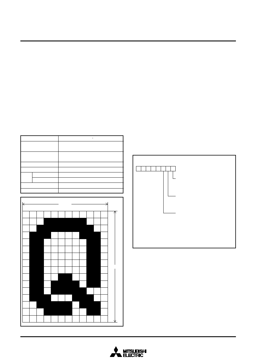
The CRT display ROM has a capacity of 3K bytes. Because 32 bytes
are required for one character data, the ROM can contain up to 96
kinds of characters.
The CRT display ROM space is broadly divided into two areas. The
[vertical 16 dots]
×
[horizontal (left side) 8 dots] data of display char-
acters are stored in addresses 3000
16
to 35FF
16
; the [vertical 16
dots]
×
[horizontal (right side) 4 dots] data of display characters are
stored in addresses 3800
16
to 3DFF
16
(refer to Figure 27). Note how-
ever that the four upper bits in the data to be written to addresses
3800
16
to 3DFF
16
must be set to "1" (by writing data F0
16
to FF
16
).
Fig. 26 Display start position of each character size
(horizontal direction)
Minimum
Medium
Large
Horizontal display start position
(4) Memory for Display
There are two types of memory for display : ROM of CRT display (ad-
dresses 3000
16
to 35FF
16
, 3800
16
to 3DFF
16
) used to store charac-
ter dot data (masked) and display RAM (addresses 2000
16
to
20B1
16
) used to specify the colors of characters to be displayed. The
following describes each type of display memory.
ROM for display (addresses 3000
16
to 35FF
16
and 3800
16
to
3DFF
16
)
The CRT display ROM contains dot pattern data for characters to be
displayed. For characters stored in this ROM to be actually dis-
played, it is necessary to specify them by writing the character code
inherent to each character (code determined based on the ad-
dresses in the CRT display ROM) into the CRT display RAM.
MITSUBISHI MICROCOMPUTERS
M37210M3-XXXSP/FP, M37210M4-XXXSP, M37211M2-XXXSP
M37210E4-XXXSP/FP, M37210E4SP/FP
SINGLE-CHIP 8-BIT CMOS MICROCOMPUTER for VOLTAGE SYNTHESIZER
with ON-SCREEN DISPLAY CONTROLLER
28
The character code used to specify a character to be displayed is
determined based on the address in the CRT display ROM in which
that character is stored.
Assume that data for one character is stored at addresses 3XX0
16
to
3XXF
16
(XX denotes 00
16
to 5F
16
) and addresses 3YY0
16
to 3YYF
16
(YY denotes 80
16
to DF
16
), then the character code for it is "XX16".
In other words, character code for any given character is configured
with two middle digits of the four-digit (hexnotated) addresses 3000
16
to 35FF
16
where data for that character is stored.
Table 6 lists the character codes.
Fig. 27 Display character stored area
bit 7
bit 0
bit 7
bit 3
bit 0
3XX0
16
+800
16
3XXF
16
+800
16
3XX0
16
0 0 0 0 0 0 0 0
0
0
1
0
0
0
0
0
0
0
0
0
0
1
0
0
0
1
0
1
0
0
0
0
0
0
0
0 1 0 1 0
1
0
0
0
1
0
0
0
0
0
0
1
0
0
0
1
1
0
0
0
0
0
0
1
0 0 1 0
0
0
0
0
1
0 0
1
0 0
0 0 0 0 0
0
0 1
0 0 0
0
0 1
0 0
0 0 0
0
0 0
0 1
0
0 0
0
0
0 0 0
0 0 0 0 0
0
0 0
3XXF
16
1 1 1 1 0 0 0 0
0
0
0
0
1
1
1
1
1
1
1
0
1
0
0
0
0
0
0
0
1
1
1
1
1
1
1
1 0 0 0 0
0
0
0
0
1
1
1
1
1
1
1
0
0
0
0
1
0
0
0
0
1
1
1
1
1 1 1 1
0
0
1
0
0
0
0
1
1
1
1 1
1
1 1
1 1 0 0 0
1 0 1 0 0
1
1 1
1 0 1
1
1 1
0 0
1 0 1
1
0 0
1 1
1
1 0
1
1
0 0 0
1 0 0 0 0
1
1 1
0 0 0 0 0
1
1
1
1
1
MITSUBISHI MICROCOMPUTERS
M37210M3-XXXSP/FP, M37210M4-XXXSP, M37211M2-XXXSP
M37210E4-XXXSP/FP, M37210E4SP/FP
SINGLE-CHIP 8-BIT CMOS MICROCOMPUTER for VOLTAGE SYNTHESIZER
with ON-SCREEN DISPLAY CONTROLLER
29
RAM for display (address 2000
16
to 20B1
16
)
The CRT display RAM is allocated at addresses 2000
16
to 20B1
16
,
and is divided into a display character code specifying part and dis-
play color specifying part for each block.
Table 7 shows the contents of the CRT display RAM.
When a character is to be displayed at the first character (leftmost)
position in block 1, for example, it is necessary to write the character
code to the seven low-order bits (bits 0 to 6) in address 2000
16
and
the color register No. to the two low-order bits (bits 0 and 1) in ad-
dress 2080
16
. The color register No. to be written here is one of the
four color registers in which the color to be displayed is set in ad-
vance. For details on color registers, refer to (5) Color Registers.
The structure of the CRT display RAM is shown in Figure 27.
Table 7. The contents of the CRT display RAM
Block
Block 1
Block 2
Display position (from left)
1st character
2nd character
3rd character
:
16th character
17th character
18th character
1st character
2nd character
3rd character
:
16th character
17th character
18th character
Color specification
2080
16
2081
16
2082
16
:
208F
16
2090
16
2091
16
2092
16
:
209F
16
20A0
16
20A1
16
20A2
16
:
20AF
16
20B0
16
20B1
16
20B2
16
:
20BF
16
Character code specification
2000
16
2001
16
2002
16
:
200F
16
2010
16
2011
16
2012
16
:
201F
16
2020
16
2021
16
2022
16
:
202F
16
2030
16
2031
16
2032
16
:
203F
16
Not used
Not used
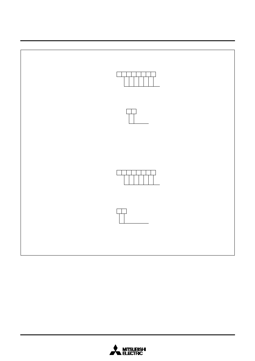
MITSUBISHI MICROCOMPUTERS
M37210M3-XXXSP/FP, M37210M4-XXXSP, M37211M2-XXXSP
M37210E4-XXXSP/FP, M37210E4SP/FP
SINGLE-CHIP 8-BIT CMOS MICROCOMPUTER for VOLTAGE SYNTHESIZER
with ON-SCREEN DISPLAY CONTROLLER
30
Fig. 28 Structure of the CRT display RAM
7
0
Character code (00
16
to 5F
16
)
Specify 96 characters
1 0
Specify color select mode
00 : Color register 0 specification
01 : Color register 1 specification
10 : Color register 2 specification
11 : Color register 3 specification
7
0
Character code (00
16
to 5F
16
)
Specify 96 characters
1
0
Color register specification
00 : Color register 0 specification
01 : Color register 1 specification
10 : Color register 2 specification
11 : Color register 3 specification
Block 1
[Color specification]
1st character : 2080
16
to
18th character : 2091
16
Block 2
[Character specification]
1st character : 2020
16
to
18th character : 2031
16
[Color specification]
1st character : 20A0
16
to
18th character : 20B1
16
[Character specification]
1st character : 2000
16
to
18th character : 2011
16
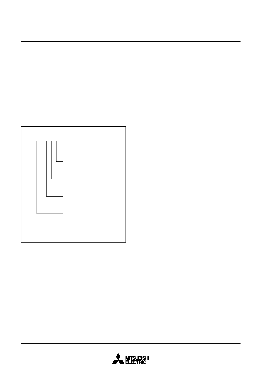
MITSUBISHI MICROCOMPUTERS
M37210M3-XXXSP/FP, M37210M4-XXXSP, M37211M2-XXXSP
M37210E4-XXXSP/FP, M37210E4SP/FP
SINGLE-CHIP 8-BIT CMOS MICROCOMPUTER for VOLTAGE SYNTHESIZER
with ON-SCREEN DISPLAY CONTROLLER
31
(5) Color Registers
The color of a displayed character can be specified by setting the
color to one of the four color registers (CO0 to CO3 : addresses
00E6
16
to 00E9
16
) and then specifying that color register with the
CRT display RAM.
There are three color outputs : R, G and B. By using a combination
of these outputs, it is possible to set 2
3
-1 (when no output) = 7 col-
ors. However, because only four color registers are available, up to
four colors can be displayed at one time.
R, G and B outputs are set by using bits 1 to 3 in the color register.
Bit 5 is used to specify whether a character output or blank output.
Figure 29 shows the structure of the color register.
(6) Multiline Display
The M37210M3-XXXSP can normally display two lines on the CRT
screen by displaying two blocks at different vertical positions.
In addition, it allows up to 16 lines to be displayed by using a CRT
interrupt.
The CRT interrupt works in such a way that when display of one
block is terminated, an interrupt request is generated.
In other words, character display for a certain block is initiated when
the scanning line reaches the display position for that block (speci-
fied with vertical position register) and when the range of that block
is exceeded, an interrupt is applied.
Note : A CRT interrupt does occurs at the end of display regardless
of display on or off. In other words, even if a block is set to off
display with the display control bit of the CRT control register
(address 00EA
16
), a CRT interrupt request occurs (refer to
Figure 30).
Fig. 29 Structure of color registers
Note : When the character bordering function is used, the contents
of this bit (bit 5) are invalied, and the OUT pin output be-
comes a border output.
Color registers 0,1,2,3
(CO0 : address 00E6
16
)
(CO1 : address 00E7
16
)
(CO2 : address 00E8
16
)
(CO3 : address 00E9
16
)
7
0
B signal output selection bit
0 : No character is output
1 : Character is output
OUT signal output selection bit (Note)
0 : OUT pin outputs character
1 : OUT pin outputs blank
G signal output selection bit
0 : No character is output
1 : Character is output
R signal output selection bit
0 : No character is output
1 : Character is output
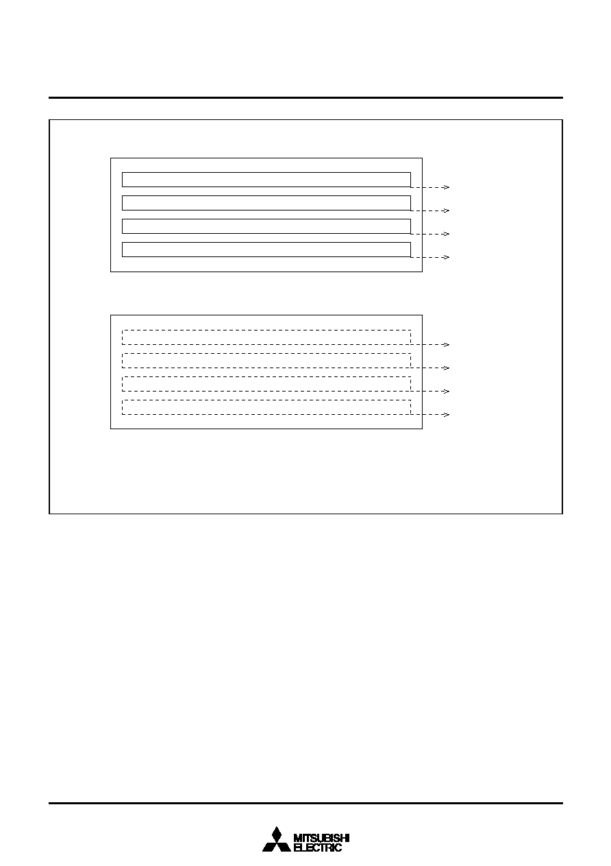
MITSUBISHI MICROCOMPUTERS
M37210M3-XXXSP/FP, M37210M4-XXXSP, M37211M2-XXXSP
M37210E4-XXXSP/FP, M37210E4SP/FP
SINGLE-CHIP 8-BIT CMOS MICROCOMPUTER for VOLTAGE SYNTHESIZER
with ON-SCREEN DISPLAY CONTROLLER
32
Fig. 30 Timing of CRT interrupt
(Note) : That is to say, "CRT interrupt" occurs even when it is off display by setting the display control flag of the CRT control
register (address 00EA
16
).
Block 2' (on display)
Block 1' (on display)
Block 2 (on display)
Block 1 (on display)
"CRT interrupt"
"CRT interrupt"
"CRT interrupt"
"CRT interrupt"
On display ("CRT interrupt" works after block)
Block 2' (off display)
Block 1' (off display)
Block 2 (off display)
Block 1 (off display)
"CRT interrupt"
"CRT interrupt"
"CRT interrupt"
"CRT interrupt"
Off display ("CRT interrupt" occurs after block)
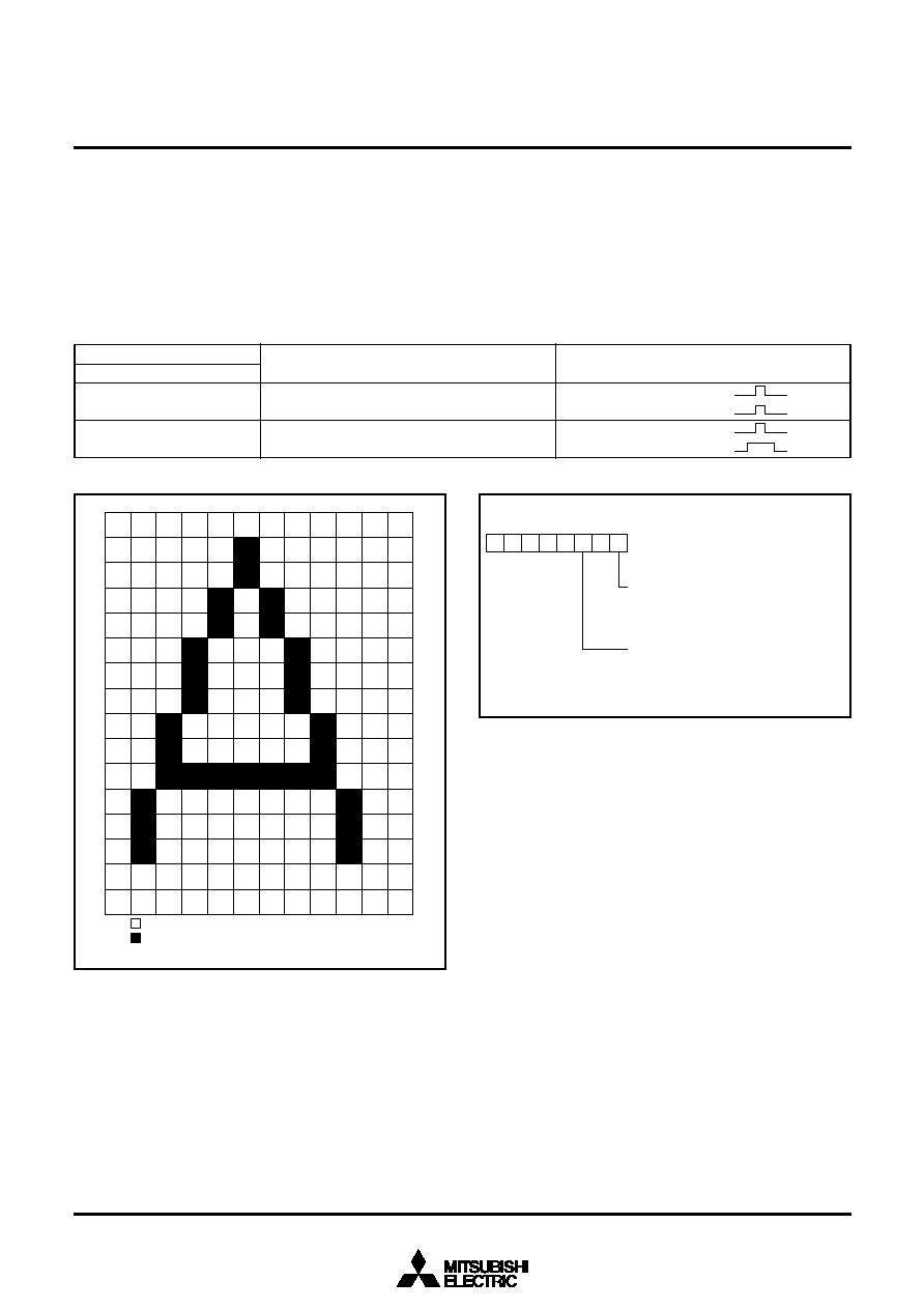
MITSUBISHI MICROCOMPUTERS
M37210M3-XXXSP/FP, M37210M4-XXXSP, M37211M2-XXXSP
M37210E4-XXXSP/FP, M37210E4SP/FP
SINGLE-CHIP 8-BIT CMOS MICROCOMPUTER for VOLTAGE SYNTHESIZER
with ON-SCREEN DISPLAY CONTROLLER
33
(7) Character Border Function
An border of a one clock (one dot) equivalent size can be added to a
character to be displayed in both horizontal and vertical directions.
The border is output from the OUT pin. In this case, bit 5 in the color
register (contents output from the OUT pin) is nullified, and the bor-
der is output from the OUT pin instead.
Fig. 31 Example of border
Fig. 32 Structure of border selection register
Border can be specified in units of block by using the border select
register (address 00E5
16
). Table 8 shows the relationship between
the values set in the border select register and the character border
function. Figure 32 shows the structure of the border select register.
is border.
is display by character data.
Table 8. The relationship between the value set in the border selection register and the character border function
Border selection register
MDn0
0
1
Functions
Ordinary
Border including character
Example of output
R, G, B output
OUT output
R, G, B output
OUT output
7
0
Border selection register
(MD : address 00E5
16
)
Block 1 OUT signal output border selection bit
0 : Same output as R, G, B is output
1 : Border output
Block 2 OUT signal output border selection bit
0 : Same output as R, G, B is output
1 : Border output
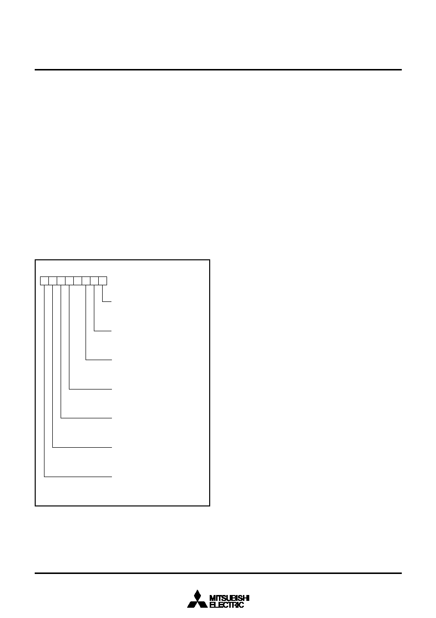
MITSUBISHI MICROCOMPUTERS
M37210M3-XXXSP/FP, M37210M4-XXXSP, M37211M2-XXXSP
M37210E4-XXXSP/FP, M37210E4SP/FP
SINGLE-CHIP 8-BIT CMOS MICROCOMPUTER for VOLTAGE SYNTHESIZER
with ON-SCREEN DISPLAY CONTROLLER
34
(8) CRT Output Pin Control
CRT output pins R, G, B and OUT are respectively shared with port
P5
2
, P5
3
, P5
4
and P5
5
. When the corresponding bits in the port P5
control register (address 00CB
16
) are cleared to "0", the pins are set
for CRT output ; when the bits are set to "1", the pins function as port
P5 (general- purpose output pins).
The polarities of CRT outputs (R, G, B and OUT, as well as H
SYNC
and V
SYNC
) can be specified by using the CRT port control register
(address 00EC
16
).
Use bits 0 to 4 in the CRT port control register to set the output po-
larities of H
SYNC
, V
SYNC
, R/G/B and OUT. When these bits are
cleared to "0", a positive polarity is selected ; when the bits are set to
"1", a negative polarity is selected.
Bits 5 to 7 in the CRT port control register are used to specify pin by
pin whether normal video signals or R-MUTE, G-MUTE, and B-
MUTE signals are output from each pin (R, G, B). When set for R-
MUTE, G-MUTE, and B-MUTE outputs, the whole background
colors of the screen become red, green, and blue.
Figure 33 shows the structure of the CRT port control register.
Fig. 33 Structure of CRT port control register
7
0
H
SYNC
input polarity selection bit
0 : Positive polarity
1 : Negative polarity
Polarity register
(CRTP : address 00EC
16
)
V
SYNC
input polarity selection bit
0 : Positive polarity
1 : Negative polarity
OUT output polarity selection bit
0 : Positive polarity
1 : Negative polarity
R pin output switch bit
0 : R signal output
1 : R-MUTE signal output
G pin output switch bit
0 : G signal output
1 : G-MUTE signal output
R/G/B output polarity selection bit
0 : Positive polarity
1 : Negative polarity
B pin output switch bit
0 : B signal output
1 : B-MUTE signal output
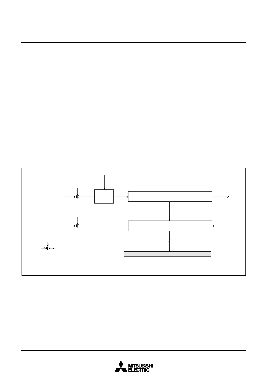
MITSUBISHI MICROCOMPUTERS
M37210M3-XXXSP/FP, M37210M4-XXXSP, M37211M2-XXXSP
M37210E4-XXXSP/FP, M37210E4SP/FP
SINGLE-CHIP 8-BIT CMOS MICROCOMPUTER for VOLTAGE SYNTHESIZER
with ON-SCREEN DISPLAY CONTROLLER
35
INTERRUPT INTERVAL DETERMINATION
FUNCTION
The M37210M3-XXXSP incorporates an interrupt interval determina-
tion circuit. This interrupt interval determination circuit has an 8-bit
binary up counter as shown in Figure 34.
Using this counter, it determines an interval or a pulse width on the
INT1 or INT2 (refer to Figure 36).
The following describes how the interrupt interval is determined.
1. The interrupt input to be determined (INT1 input or INT2 input) is
selected by using bit 2 in the interrupt interval determination con-
trol register (address 00D8
16
). When this bit is cleared to "0", the
INT1 input is selected ; when the bit is set to "1", the INT2 input is
selected.
2. When the INT1 input is to be determined, the polarity is selected
by using bit 3 of the interrupt interval determination control regis-
ter ; when the INT2 input is to be determined, the polarity is se-
lected by using bit 4 of the interrupt interval determination control
register.
When the relevant bit is cleared to "0", determination is made of
the interval of a positive polarity (rising transition) ; when the bit is
set to "1", determination is made of the interval of a negative po-
Fig. 34 Block diagram of interrupt interval determination circuit
Note : The pulse width of external interrupt INT1 and INT2 needs 5 or more machine cycles.
Data bus
RE
1
INT1
(Note)
RE
0
RE
2
INT2
32
µ
s
8
8
8-bit binary up counter
Interrupt interval determination register
64
µ
s
Address 00D7
16
Control
circuit
Selection gate : Connected to black
colored side at reset.
RE : Interrupt interval determination control register
larity (falling transition).
3. The reference clock is selected by using bit 1 of the interrupt inter-
val determination control register. When the bit is cleared to "0", a
64
m
s clock is selected ; when the bit is set to "1", a 32
µ
s clock is
selected (based on an oscillation frequency of 4MHz in either
case).
4. Simultaneously when the input pulse of the specified polarity (ris-
ing or falling transition) occurs on the INT1 pin (or INT2 pin), the 8-
bit binar y up counter starts counting up with the selected
reference clock (64
µ
s or 32
µ
s).
5. Simultaneously with the next input pulse, the value of the 8-bit bi-
nary up counter is loaded into the determination register (address
00D7
16
) and the counter is immediately reset (00
16
). The refer-
ence clock is input in succession even after the counter is reset,
and the counter restarts counting up from "00
16
".
6. When count value "FE
16
" is reached, the 8-bit binary up counter
stops counting. Then, simultaneously when the next reference
clock is input, the counter sets value "FF
16
" to the determination
register.
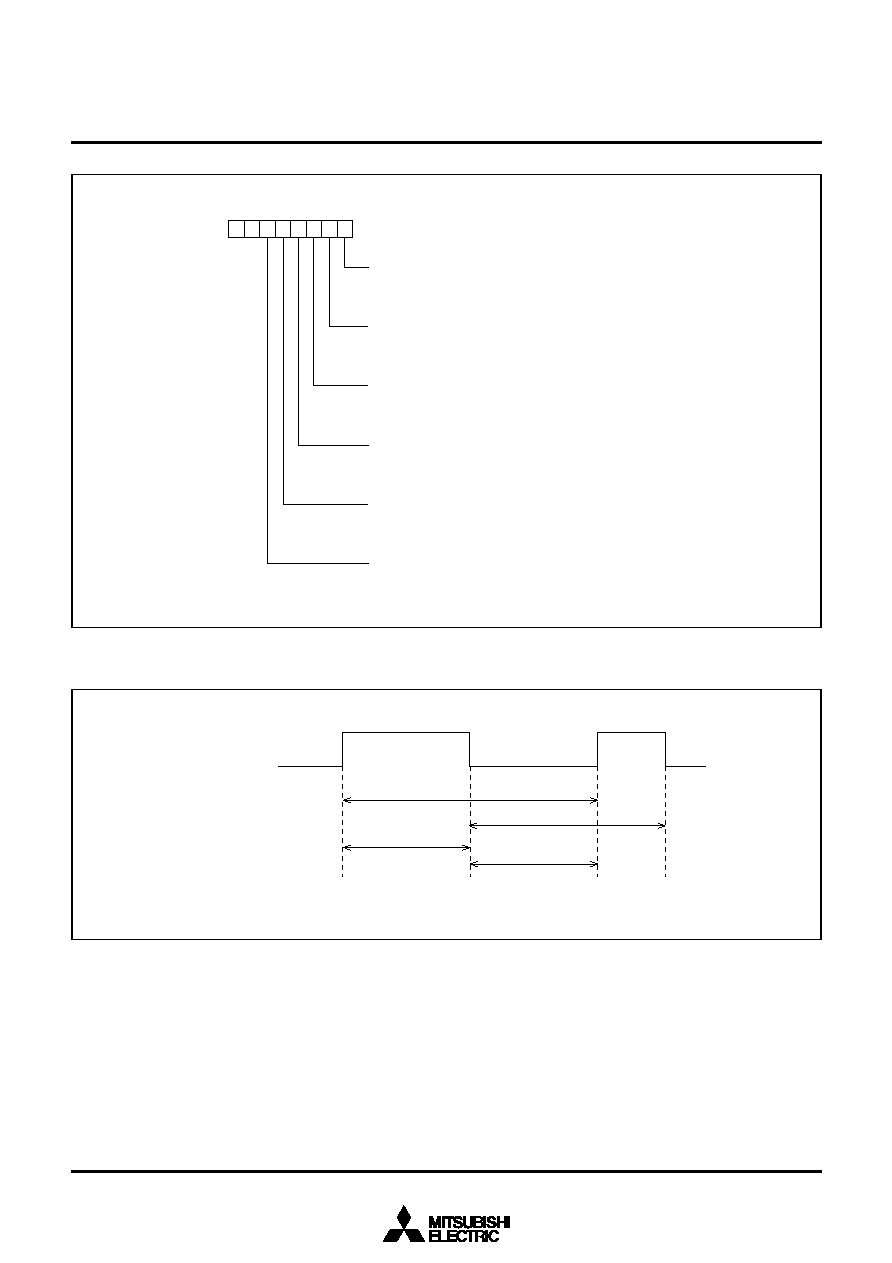
MITSUBISHI MICROCOMPUTERS
M37210M3-XXXSP/FP, M37210M4-XXXSP, M37211M2-XXXSP
M37210E4-XXXSP/FP, M37210E4SP/FP
SINGLE-CHIP 8-BIT CMOS MICROCOMPUTER for VOLTAGE SYNTHESIZER
with ON-SCREEN DISPLAY CONTROLLER
36
RE
i
: Bits
i
(
i
= 3, 4, 5) of interrupt space distinguish control register (address 00D8
16
)
Fig. 36 Interrupt space distinguish control register setting value and the measuring interval
Fig. 35 Structure of interrupt space distinguish control register
count interval
INT1 or 2 input
RE
5
0
0
1
1
RE
4
(RE
3
)
0
1
0
1
INT2 pin input polarity switch bit
0 : Positive polarity input
1 : Negative polarity input
Interrupt interval determination mode switch bit
0 : Interrupt interval determination mode
1 : Pulse width determination mode
INT1 pin input polarity switch bit
0 : Positive polarity input
1 : Negative polarity input
External interrupt input pin selection bit
0 : INT1 input
1 : INT2 input
Reference clock selection bit
(At f (X
IN
) = 4MH
Z)
0 : 64
m
s
1 : 32
m
s
Interrupt interval determination circuit operation control bit
0 : Stop
1 : Operation
Interrupt interval determination control register
(RE : address 00D8
16
)
7
0
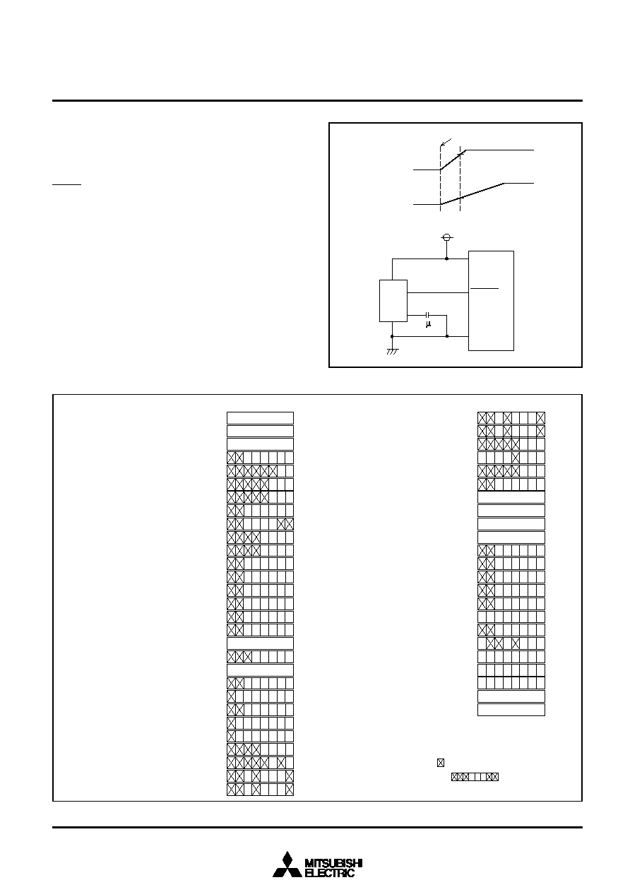
MITSUBISHI MICROCOMPUTERS
M37210M3-XXXSP/FP, M37210M4-XXXSP, M37211M2-XXXSP
M37210E4-XXXSP/FP, M37210E4SP/FP
SINGLE-CHIP 8-BIT CMOS MICROCOMPUTER for VOLTAGE SYNTHESIZER
with ON-SCREEN DISPLAY CONTROLLER
37
RESET CIRCUIT
The M37210M3-XXXSP is reset according to the sequence shown in
Figure 39. It starts the program from the address formed by using the
content of address FFFF
1 6
as the high order address and the con-
tent of the address FFFE
16
as the low order address, when the
RESET pin is held at "L" level for no less than 2
µ
s while the power
voltage is 5V ± 10% and the crystal oscillator oscillation is stable and
then returned to "H" level. The internal initializations following reset
are shown in Figure 37.
An example of the reset circuit is shown in Figure 38. The reset input
voltage must be kept below 0.6V until the supply voltage surpasses
4.5V.
Fig. 38 Example of reset circuit
Fig. 37 Internal state at reset
Notes 1 : Since the contents of both registers other than those listed
above and the RAM are undefined at reset, it is necessary to
set initial values.
"0" is read from all bits which is not used.
2 : The M37211M2-XXXSP is
3 : The M37211M2-XXXSP dose not have this register.
Power on
Reset input
voltage 0V
4.5V
0.6V
M51953AL
1
5
4
3
Vcc
RESET
Vss
M37210M4-XXXSP
27
30
26
Power source
voltage 0V
0.1 F
...
00
16
00
16
00
16
0 0 0 0 0
0 0 0 0
Address
C o n t e n t s o f a d d r e s s
F F F E
1 6
00
16
(1) Port P0 directional register
(2) Port P1 directional register
(3) Port P2 directional register
(4) Port P3
(5) Port P3 directional register
(6) Port P4
(7) Port P4 directional register
(8) Port P5
(9) Port P5 directional register
(10) Port P6
(11) Port P6 directional register
(12) 14DA-L register
(13) PWM0 register
(14) PWM1 register
(15) PWM2 register
(16) PWM3 register
(17) PWM4 register
(18) PWM output control register 1
(19)
(20)
(21)
( 0 0 C 1
16
)
( 0 0 C 3
16
)
( 0 0 C 5
16
)
( 0 0 C 6
16
)
( 0 0 C 7
16
)
( 0 0 C 8
16
)
( 0 0 C 9
16
)
( 0 0 C A
16
)
( 0 0 C B
16
)
( 0 0 C C
16
)
( 0 0 C D
16
)
( 0 0 C F
16
)
( 0 0 D 0
16
)
( 0 0 D 1
16
)
( 0 0 D 2
16
)
( 0 0 D 3
16
)
( 0 0 D 4
16
)
( 0 0 D 5
16
)
( 0 0 D 6
16
)
( 0 0 D 7
16
)
( 0 0 D 8
16
)
( 0 0 D C
16
)
( 0 0 E 0
16
)
( 0 0 E 1
16
)
( 0 0 E 2
16
)
( 0 0 E 4
16
)
( 0 0 E 5
16
)
( 0 0 E 6
16
)
( 0 0 E 7
16
)
0 0
0 0 0
1 1 1 1
00
16
0 0 0
0
1 1 1 1
0 0 0 0
0
0
0
0
0
0 0 0 0
0
0
(22) Serial I/O mode register
(23) Horizontal position register
(24)
Vertical position register 1
(25)
Vertical position register 2
(26) Character size register
(27) Border selection register
(28) Color register 0
(29) Color register 1
Interrupt interval
determination register
Interrupt interval
determination control register
0 0 0
0
0 0 0
0
0 0 0 0 0
(30) Color register 2
(31) Color register 3
(32) CRT control register
(33) CRT port control register
(34) A-D mode register
(35) A-D control register
(36) Timer 1
(37) Timer 2
(38) Timer 3
(39) Timer 4
(40) Timer 12 mode register
(41) Timer 34 mode register
(42) PWM5 register
(43) PWM6 register (Note 3)
(44) PWM7 register (Note 3)
(45) CPU mode register
(46) Interrupt request register 1
(47) Interrupt request register 2
(48) Interrupt control register 1
(49) Interrupt control register 2
(50) Processor status register
(51) Program counter
( 0 0 E 8
16
)
( 0 0 E 9
16
)
( 0 0 E A
16
)
( 0 0 E C
16
)
( 0 0 E E
16
)
( 0 0 E F
16
)
( 0 0 F 0
16
)
( 0 0 F 1
16
)
( 0 0 F 2
16
)
( 0 0 F 3
16
)
( 0 0 F 4
16
)
( 0 0 F 5
16
)
( 0 0 F 6
16
)
( 0 0 F 7
16
)
( 0 0 F 8
16
)
( 0 0 F B
16
)
( 0 0 F C
16
)
( 0 0 F D
16
)
( 0 0 F E
16
)
( 0 0 F F
16
)
( P S )
( P C
M
)
( P C
L
)
0 0 0
0 0
0 0 0
0
0 0 0
0
0 0 0
0 0 0
0 0 0
0
0 0 0
0 0 0 0 0
0 0 0 0 0
0
1 1 1 0 0
1 1 1
0 0 0 0 0
0
0
0 0 0
0
1
FF
16
07
16
FF
16
07
16
0 0
0
0 0 0
0
0
0
PWM output control
register 2(Note 2)
C o n t e n t s o f a d d r e s s
F F F F
1 6
0 0 0
...
...
...
...
...
...
...
...
...
...
...
...
...
...
...
...
...
...
...
...
...
...
...
...
...
...
...
...
...
...
...
...
...
...
...
...
...
...
...
...
...
...
...
...
...
...
...
...
...
...
...
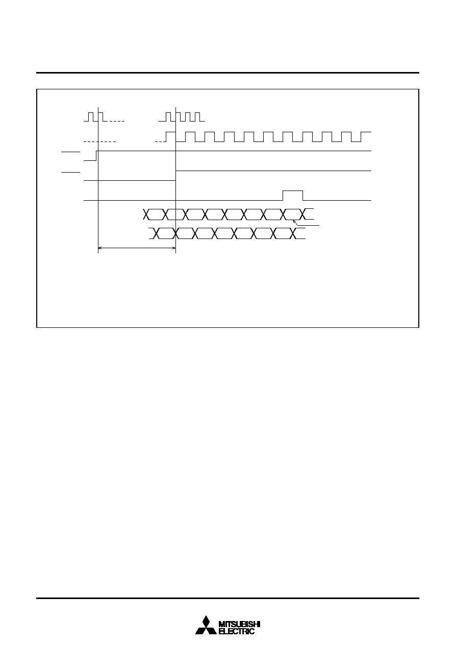
MITSUBISHI MICROCOMPUTERS
M37210M3-XXXSP/FP, M37210M4-XXXSP, M37211M2-XXXSP
M37210E4-XXXSP/FP, M37210E4SP/FP
SINGLE-CHIP 8-BIT CMOS MICROCOMPUTER for VOLTAGE SYNTHESIZER
with ON-SCREEN DISPLAY CONTROLLER
38
Fig. 39 Reset sequence
?
PC
H
PC
L
PS
AD
L
AD
H
?
?
00,S 00,S-1 00,S-2 FFFE
FFFF
?
X
IN
RESET
Internal RESET
SYNC
Address
Data
32768 count of X
IN
clock cycle (Note 3)
Reset address from the vector table
AD
H,
AD
L
Note 1 : f (X
IN
) and f (
) are in the relationship : f (X
IN
) = 2 · f (
).
2 : A question mark (?) indicates an undefined state that
depends on the previous state.
3 : Immediately after a reset, FF
16
is automatically set in
timer 3 and 07
16
in timer 4 and timer 4, timer 3 and the
clock (f (X
IN
) divided by 16) are connected in series.
Reset state is canceled by the overflow signal of timer 4.

MITSUBISHI MICROCOMPUTERS
M37210M3-XXXSP/FP, M37210M4-XXXSP, M37211M2-XXXSP
M37210E4-XXXSP/FP, M37210E4SP/FP
SINGLE-CHIP 8-BIT CMOS MICROCOMPUTER for VOLTAGE SYNTHESIZER
with ON-SCREEN DISPLAY CONTROLLER
39
I/O PORTS
(1) Port P0
Port P0 is an 8-bit I/O port with N-channel open-drain output.
As shown in the memory map (Figure 3), port P0 can be ac-
cessed at zero page memory address 00C0
16
.
Port P0 has a directional register (address 00C1
16
) which can be
used to program each individual bit as input ("0") or as output
("1"). If the pins are programmed as output, the output data is
latched to the port register and then output. When data is read
from the output port the output pin level is not read, only the
latched data in the port register is read. This allows a previously
output value to be read correctly even though the output voltage
level is shifted up or down.
Pins set as input are in the floating state and the signal levels can
thus be read. When data is written into the input port, the data is
latched only to the port latch and the pin still remains in the float-
ing state.
Ports P0
0
-P0
3
are in common with 6-bit PWM outputs PWM4-
PWM7. For the M37211M2, ports P0
0
and P0
1
are in common
with 6-bit PWM outputs PWM4 and PWM5.
(2) Port P1
Port P1 has basically the same function as port P0 except the
output structure is CMOS output. But, pins P1
5
-P1
7
are input
ports and in common with analog input pins A-D1-A-D3.
(3) Port P2
Port P2 has basically the same function as port P1.
(4) Port P3
Port P3 are a 2-bit I/O port and a 4-bit input port with function
similar to port P2, but the output structure of P3
0
, P3
1
is CMOS
output.
P3
2
, P3
3
are in common with the external clock input pins of timer
2 and 3.
P3
4
, P3
5
are in common with the external interrupt input pins
INT1, INT2 and P3
5
with the analog input pin of A-D comparator
A-D4.
(5) Port P4
Port P4 are a 2-bit I/O port and a 1-bit input port with function
similar to port P2, but the output structure is N-channel open-
drain output.
When a serial I/O function is selected, P4
0
-P4
2
are in common
with pins S
OUT
, S
CLK
and S
IN
.
(6) OSC1, OSC2 pins
Clock input/output pins for CRT display function.
(7) H
SYNC
, V
SYNC
pins
H
SYNC
is a horizontal synchronizing signal input pin for CRT dis-
play.
V
SYNC
is a vertical synchronizing signal input pin for CRT display.
(8) R, G, B, OUT pins
This is an 4-bit output pin for CRT display and in common with
P5
2
-P5
5
.
(9) Port P6
Port P6 is an 4-bit output port with function similar to port P0, but
the output structure is N-channel opendrain output.
This port is in common with 6-bit PWM output pin PWM0-PWM3.
(10) D-A pin
This is a 14-bit PWM output pin.
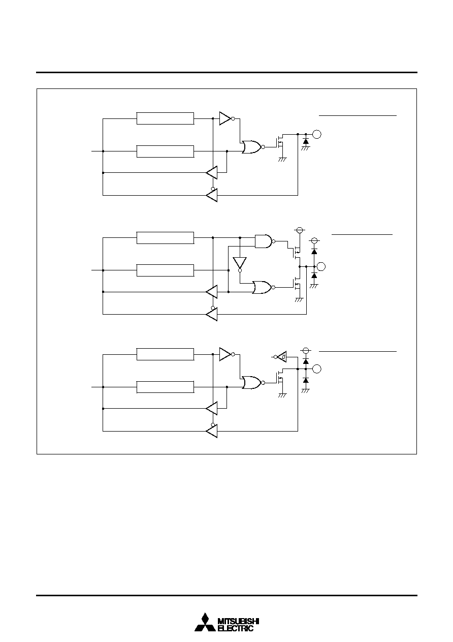
MITSUBISHI MICROCOMPUTERS
M37210M3-XXXSP/FP, M37210M4-XXXSP, M37211M2-XXXSP
M37210E4-XXXSP/FP, M37210E4SP/FP
SINGLE-CHIP 8-BIT CMOS MICROCOMPUTER for VOLTAGE SYNTHESIZER
with ON-SCREEN DISPLAY CONTROLLER
40
Fig. 40 I/O pin block diagram (1)
Note : P4
0
, P4
1
can also be used as
serial I/O pins.
Directional register
Port latch
Data bus
CMOS 3-state output
Port P1
0
P1
4
, P2, P3
0
, P3
1
Port P1
0
P1
4
, P2, P3
0
, P3
1
Directional register
Port latch
Data bus
N-channel open-drain output
Port P4
0
,P4
1
Directional register
Port latch
Data bus
N-channel open-drain output
Port P0
Port P0
Port P4
0
,P4
1
S
IN
/S
CLK
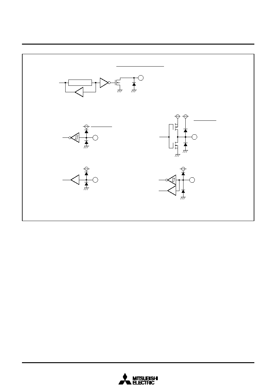
MITSUBISHI MICROCOMPUTERS
M37210M3-XXXSP/FP, M37210M4-XXXSP, M37211M2-XXXSP
M37210E4-XXXSP/FP, M37210E4SP/FP
SINGLE-CHIP 8-BIT CMOS MICROCOMPUTER for VOLTAGE SYNTHESIZER
with ON-SCREEN DISPLAY CONTROLLER
41
Fig. 41 I/O pin block diagram (2)
Note : P1
5
P1
7
are in common with input Pins for A-D comparator.
P3
2
, P3
3
are in common with timer inputs.
P3
4
, P3
5
are in common with external interrupt inputs.
P4
2
is in common with input pins of serial I/O pins.
Note : Pins R, G, B, and OUT can also be
used as output ports P5
2
P5
5
.
N-channel open-drain output
Port P6
H
SYNC
, V
SYNC
Schmitt input
H
SYNC
, V
SYNC
CMOS output
D-A, R, G, B, OUT
Data bus
Port P1
5
P1
7
Port P1
5
P1
7
Internal circuit
D-A, R, G, B, OUT
Data bus
Ports P3
2
P3
5
, P4
2
TIM2, TIM3,
INT1, INT2,
or S
IN
Internal circuit
Port P6
Data bus
Port latch
Note : P6 can also be used as
6-bit PWM output pins.
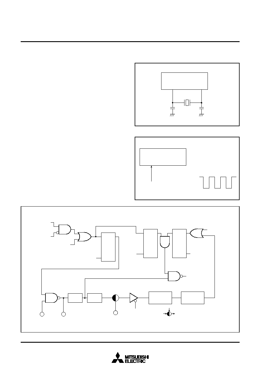
MITSUBISHI MICROCOMPUTERS
M37210M3-XXXSP/FP, M37210M4-XXXSP, M37211M2-XXXSP
M37210E4-XXXSP/FP, M37210E4SP/FP
SINGLE-CHIP 8-BIT CMOS MICROCOMPUTER for VOLTAGE SYNTHESIZER
with ON-SCREEN DISPLAY CONTROLLER
42
CLOCK GENERATING CIRCUIT
The built-in clock generating circuit is shown in Figure 44.
When the STP instruction is executed, the internal clock
stops os-
cillating at "H" level. At the same time, timers 3 and 4 are connected
in hardware and "FF
16
" is set in the timer 3, "07
16
" is set in the timer
4. Select f(X
IN
)/16 as the timer 3 count source (set bit 0 of the timer
34 mode register to "0" before the execution of the STP instruction).
And besides, set the timer 3 and timer 4 interrupt enable bits to dis-
abled ("0") before execution of the STP instruction.
The oscillator is restarted when an external interrupt is accepted.
However, the internal clock
keeps its "H" level until timer 4 over-
flows.
This is because the oscillator needs a set-up period if a ceramic reso-
nator or a quartz-crystal oscillator is used.
When the WIT instruction is executed, the internal clock
stops in the
"H" level but the oscillator continues running. This wait state is
cleared when an interrupt is accepted (Note). Since the oscillation
does not stop, the next instructions are executed at once.
To return from the stop or the wait state, set the interrupt enable bit to
"1" before executing the STP or the WIT instruction.
Note : In the wait mode, the following interrupts are invalid.
(1) V
SYNC
interrupt
(2) CRT interrupt
(3) Timer 2 interrupt using P3
2
/TIM2 pin input as count source
(4) Timer 3 interrupt using P3
3
/TIM3 pin input as count source
(5) Timer 4 interrupt using f(X
IN
)/2 as count source
The circuit example using a ceramic resonator (or a quartz crystal
oscillator) is shown in Figure 42.
Use the circuit constants in accordance with the resonator
manufacture's recommended values.
Fig. 44 Clock generating circuit block diagram
Interrupt request
Interrupt
disable flag I
Reset
S
Q
R
S
Q
R
S
Q
R
Reset
STP instruction
Timer 4
Timer 3
1/2
1/8
Internal clock
TIM3
T34M
2
T34M
0
X
IN
X
OUT
WIT
instruction
STP instruction
Selection gate: Connected to black
colored side at reset.
Fig. 42 Ceramic resonator circuit example
Fig. 43 External clock input circuit example
M37210M3-XXXSP
X
IN
X
OUT
24
25
C
IN
C
OUT
M37210M3-XXXSP
X
IN
External oscillation
circuit
Vcc
Vss
24
The example of external clock usage is shown in Figure 43 X
IN
is the
input, and X
OUT
is open.
MITSUBISHI MICROCOMPUTERS
M37210M3-XXXSP/FP, M37210M4-XXXSP, M37211M2-XXXSP
M37210E4-XXXSP/FP, M37210E4SP/FP
SINGLE-CHIP 8-BIT CMOS MICROCOMPUTER for VOLTAGE SYNTHESIZER
with ON-SCREEN DISPLAY CONTROLLER
43
DATA REQUIRED FOR MASK ORDERS
The following are necessary when ordering a mask ROM production.
(1) Mask ROM Order Confirmation Form
(2) Mark Specification Form
(3) Data to be written to ROM, in EPROM form (28-pin DIP type
27256, three identical copies)
PROM Programming Method
The built-in PROM of the blank One Time PROM version and built-in
EPROM version can be read or programmed with a general-purpose
PROM programmer using a special programming adapter.
Product
M37210E4SP
M37210E4FP
Name of Programming Adapter
PCA4754
PCA4756
The PROM of the blank One Time PROM version is not tested
or screened in the assembly process and following processes. To
ensure proper operation after programming, the procedure shown
in Figure 45 is recommended to verify programming.
Fig. 45 Programming and testing of One Time PROM version
Programming with
PROM programmer
Screening (Caution)
(150 for 40 hours)
Verification with
PROM programmer
Functional check in target device
Caution : The screening temperature is far higher than the
storage temperature. Never expose to 150°C ex-
ceeding 100 hours.
PROGRAMMING NOTES
(1) The divide ratio of the timer is 1/ (n + 1).
(2) Even though the BBC and BBS instructions are executed imme-
diately after the interrupt request bits are modified (by the pro-
gram), those instructions are only valid for the contents before
the modification. At least one instruction cycle is needed (such as
an NOP) between the modification of the interrupt request bits
and the execution of the BBC and BBS instructions.
(3) After the ADC and SBC instructions are executed (indecimal op-
eration mode), one instruction cycle (such as an NOP) is needed
before the SEC, CLC, or CLD instructions are executed.
(4) An NOP instruction is needed immediately after the execution of
a PLP instruction.
(5) In order to avoid noise and latch-up, connect a bypass capacitor
(
0.1
µ
F) directly between the V
CC
pin and V
SS
pin using a thick
wire.
MITSUBISHI MICROCOMPUTERS
M37210M3-XXXSP/FP, M37210M4-XXXSP, M37211M2-XXXSP
M37210E4-XXXSP/FP, M37210E4SP/FP
SINGLE-CHIP 8-BIT CMOS MICROCOMPUTER for VOLTAGE SYNTHESIZER
with ON-SCREEN DISPLAY CONTROLLER
44
Parameter
Power source voltage (Note 4) During the CPU and the CRT operation
Power source voltage
"H" input voltage P0
0
P0
7
, P1
0
P1
7
, P2
0
P2
7
,
P3
0
P3
5
, P4
0
P4
2
, H
SYNC
,
V
SYNC
, RESET, X
IN
, OSC1,
TIM2, TIM3, INT1, INT2, S
IN
, S
CLK
"L" input voltage P0
0
P0
7
, P1
0
P1
7
, P2
0
P2
7
,
P3
0
P3
5
, P4
0
P4
2
"L" input voltage TIM2, TIM3, INT1, INT2, S
IN
, S
CLK
,
H
SYNC
, V
SYNC
, RESET, X
IN
, OSC1
"H" average output current (Note 1) R, G, B, OUT,
P1
0
P1
4
, P2
0
P2
7
, P3
0
, P3
1
, D-A
"L" average output current (Note 2) R, G, B, OUT, P1
0
P1
4
,
P2
0
P2
3
, P3
0
, P3
1
, P4
0
, P4
1
, D-A
"L" average output current (Note 2) P6
0
P6
3
, P0
0
P0
7
"L" average output current (Note 3) P2
4
P2
7
Oscillation frequency (for CPU operation)(Note 5)
Oscillation frequency (for CRT display)
Input frequency TIM2, TIM3, INT1, INT2
Input frequency S
CLK
Parameter
Power source voltage
Input voltage CNV
SS
Input voltage P0
0
P0
7
, P1
0
P1
7
, P2
0
P2
7
,
P3
0
P3
5
, P4
0
P4
2
, H
SYNC
,
V
SYNC
, RESET, OSC1, X
IN
Output voltage P1
0
P1
4
, P2
0
P2
7
, P3
0
, P3
1
,
P4
0
, P4
1
, R, G, B, OUT, D-A,
X
OUT
, OSC2
Output voltage P6
0
P6
3
, P0
0
P0
7
"H" average output current R, G, B, OUT, P1
0
P1
4
,
P2
0
P2
3
, P3
0
, P3
1
,
D-A
"L" average output current R, G, B, OUT, P1
0
P1
4
,
P2
0
P2
3
, P3
0
, P3
1
, P4
0
, P4
1
D-A
"L" average output current P6
0
P6
3
, P0
0
P0
7
"L" average output current P2
4
P2
7
Power dissipation
Operating temperature
Storage temperature
ABSOLUTE MAXIMUM RATINGS
Symbol
V
CC
V
SS
V
IH
V
IL
V
IL
I
OH
I
OL1
I
OL2
I
OL3
f
CPU
f
CRT
fhs
fhs
Min.
4.5
0
0.8V
CC
0
0
3.6
4.0
Max.
5.5
0
V
CC
0.4V
CC
0.2V
CC
1
2
1
10
8.1
6.0
100
1
Limits
Unit
V
V
V
V
V
mA
mA
mA
mA
MHz
MHz
kHz
MHz
(V
CC
= 5V ± 10%, Ta = 10 to 70°C unless otherwise noted)
RECOMMENDED OPERATING CONDITIONS
Symbol
V
CC
V
I
V
I
V
O
V
O
I
OH
I
OL1
I
OL2
I
OL3
Pd
Topr
Tstg
Conditions
All voltages are based on
V
SS
.
Output transistors are
cut off.
Ta = 25°C
Ratings
0.3 to 6
0.3 to 6
0.3 to V
CC
+ 0.3
0.3 to V
CC
+ 0.3
0.3 to 13
0 to 1 (Note 1)
0 to 2 (Note 2)
0 to 1 (Note 2)
0 to 10 (Note 3)
550
10 to 70
40 to 125
Unit
V
V
V
V
V
mA
mA
mA
mA
mW
°C
°C
Typ.
5.0
0
4.0
5.0
Notes 1 : The total current that flows out of the IC should be 20mA (max.).
2 : The total of I
OL1
and I
OL2
should be 30mA (max.).
3 : The total of I
OL
of port P2
4
-P2
7
should be 20mA (max.).
4 : Connect 0.022
µ
F or more capacitor externally between the V
CC
V
SS
power source pins so as to reduce power
source noise.
Also connect 0.068
µ
F or more capacitor externally between the V
CC
CNV
SS
pins.
5 : Use a quartz-crystal oscillator or a ceramic resonator for CPU oscillation circuit.
MITSUBISHI MICROCOMPUTERS
M37210M3-XXXSP/FP, M37210M4-XXXSP, M37211M2-XXXSP
M37210E4-XXXSP/FP, M37210E4SP/FP
SINGLE-CHIP 8-BIT CMOS MICROCOMPUTER for VOLTAGE SYNTHESIZER
with ON-SCREEN DISPLAY CONTROLLER
45
Parameter
Power source current
"H" output voltage P1
0
P1
4
, P2
0
P2
7
,
P3
0
, P3
1
, R, G, B, OUT, D-A
"L" output voltage P1
0
P1
4
, P2
0
P2
3
, P3
0
, P3
1
,
P4
0
, P4
1
, R, G, B, OUT, D-A
"L" output voltage P6
0
P6
3
, P0
0
P0
7
"L" output voltage P2
4
P2
7
Hysteresis RESET
Hysteresis (Note) H
SYNC
, V
SYNC
, TIM2, TIM3,
INT1, INT2, S
IN
, S
CLK
"H" input leak current RESET, P0
0
P0
7
,
P1
0
P1
7
, P2
0
P2
7
,
P3
0
P3
5
, P4
0
P4
2
, H
SYNC
, V
SYNC
"L" input leak current RESET, P0
0
P0
7
,
P1
0
P1
7
, P2
0
P2
7
, P3
0
P3
5
,
P4
0
P4
2
, P6
0
P6
3
, H
SYNC
, V
SYNC
"H" input leak current
P6
0
P6
3
, P0
0
P0
7
ELECTRIC CHARACTERISTICS
(V
CC
= 5V ± 10%, V
SS
= 0V, Ta = 10 to 70°C, f (X
IN
) = 4MHz unless otherwise noted)
C
R
T
C
R
T
OFF
ON
OFF
ON
Min.
2.4
Limits
Typ.
10
20
20
30
0.5
0.5
Test conditions
V
CC
= 5.5V
f (X
IN
) = 4MHz
V
CC
= 5.5V
f (X
IN
) = 8MHz
At stop mode
V
CC
= 4.5V
I
OH
= 0.5mA
V
CC
= 4.5V
I
OL
= 0.5mA
V
CC
= 4.5V
I
OL
= 0.5mA
V
CC
= 4.5V
I
OL
= 10.0mA
V
CC
= 5.0V
V
CC
= 5.0V
V
CC
= 5.5V
V
I
= 5.5V
V
CC
= 5.5V
V
I
= 0V
V
CC
= 5.5V
V
O
= 12V
Symbol
I
CC
V
OH
V
OL
V
T
+ V
T
I
IZH
I
IZL
I
OZH
Note : P3
2
P3
5
, have the hysteresis when these pins are used as interrupt input pins or timer input pins.
P4
0
P4
2
have the hysteresis when these pins are used as serial I/O ports.
Max.
20
40
40
60
300
0.4
0.4
3.0
0.7
1.3
5
5
10
Unit
mA
mA
µ
A
V
V
V
µ
A
µ
A
µ
A
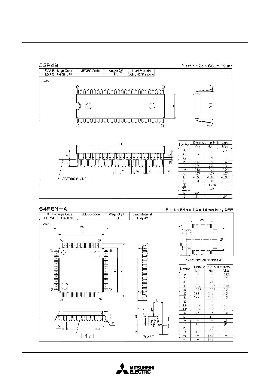
MITSUBISHI MICROCOMPUTERS
M37210M3-XXXSP/FP, M37210M4-XXXSP, M37211M2-XXXSP
M37210E4-XXXSP/FP, M37210E4SP/FP
SINGLE-CHIP 8-BIT CMOS MICROCOMPUTER for VOLTAGE SYNTHESIZER
with ON-SCREEN DISPLAY CONTROLLER
46
PACKAGE OUTLINE
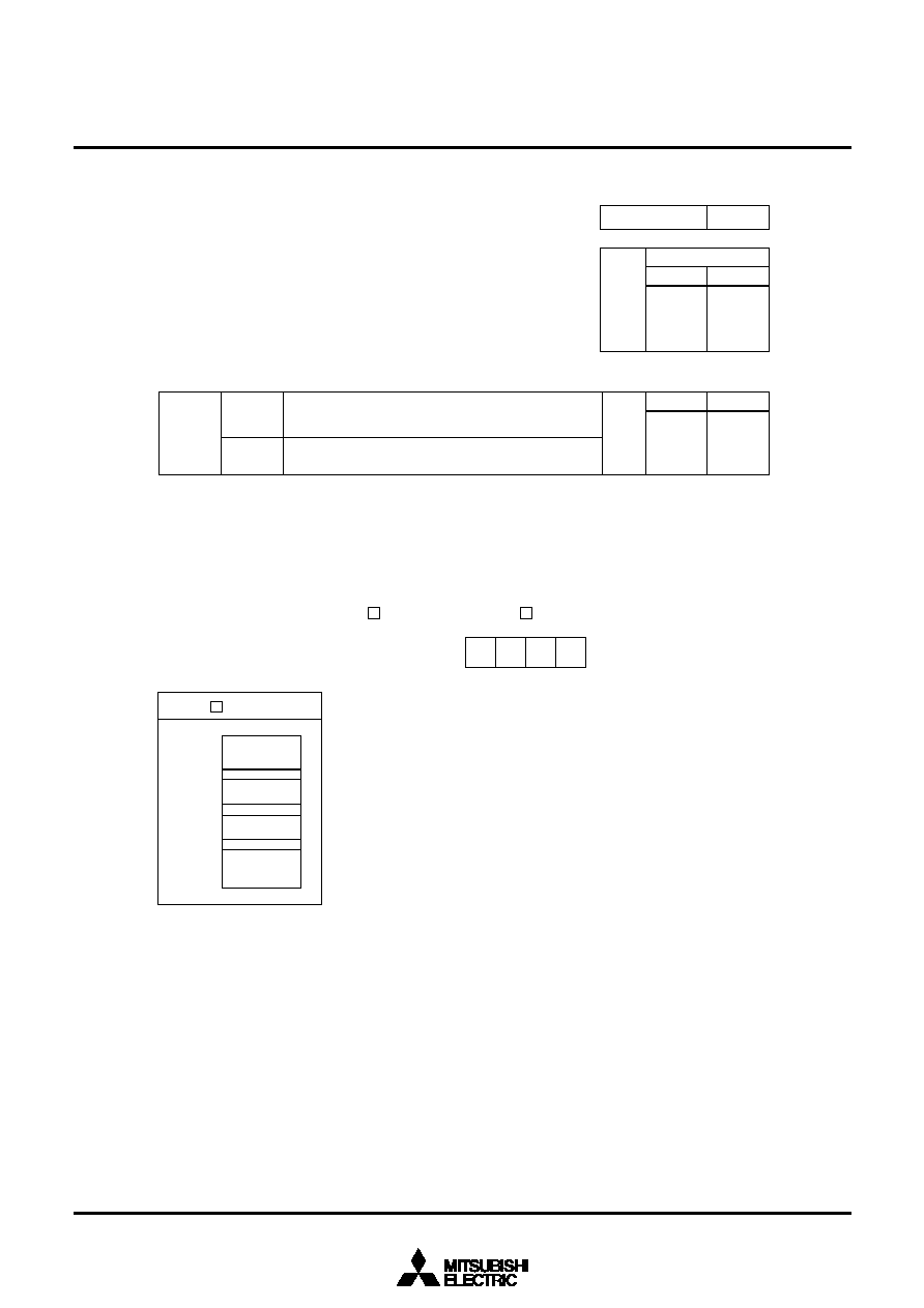
MITSUBISHI MICROCOMPUTERS
M37210M3-XXXSP/FP, M37210M4-XXXSP, M37211M2-XXXSP
M37210E4-XXXSP/FP, M37210E4SP/FP
SINGLE-CHIP 8-BIT CMOS MICROCOMPUTER for VOLTAGE SYNTHESIZER
with ON-SCREEN DISPLAY CONTROLLER
47
GZZSH0609B < 25C0 >
740 FAMILY MASK ROM CONFIRMATION FORM
SINGLE-CHIP MICROCOMPUTER M37210M3-XXXSP/FP
MITSUBISHI ELECTRIC
Mask ROM number
Date :
Supervisor
signature
Receipt
Section head
signature
g
Customer
Company
name
Date
issued
Date :
TEL
( )
Note : Please fill in all items marked
g
.
Submitted by
Supervisor
Issuance
signature
g
1. Confirmation
Specify the name of the product being ordered and the type of EPROMs submitted.
Three EPROMs are required for each pattern.
If at least two of the three sets of EPROMs submitted contain identical data, we will produce masks based on
this data. We shall assume the responsibility for errors only if the mask ROM data on the products we produce
differs from this data. Thus, extreme care must be taken to verify the data in the submitted EPROMs.
Checksum code for entire EPROM
(hexadecimal notation)
27256
EPROM address
0000
16
Product name
ASCII code :
`M37210M3 '
ROM (12K bytes)
000F
16
15FF
16
1800
16
1DFF
16
Set "FF
16
" in the shaded area.
Write the ASCII codes that indicates the product name of "M37210M3" to addresses 0000
16
to 000F
16
.
(1)
(2)
EPROM type (indicate the type used)
1000
16
Character ROM1
5000
16
7FFF
16
Character ROM2
g
2. Mark specification
Mark specification must be submitted using the correct form for the type package being ordered fill out the appropriate
mark specification form (52P4B for M37210M3-XXXSP; 64P6N for M37210M3-XXXFP) and attach to the mask ROM
confirmation form.
g
3. Comments
(1/3)
Microcomputer name : M37210M3-XXXSP M37210M3-XXXFP
MITSUBISHI MICROCOMPUTERS
M37210M3-XXXSP/FP, M37210M4-XXXSP, M37211M2-XXXSP
M37210E4-XXXSP/FP, M37210E4SP/FP
SINGLE-CHIP 8-BIT CMOS MICROCOMPUTER for VOLTAGE SYNTHESIZER
with ON-SCREEN DISPLAY CONTROLLER
48
GZZSH0609B < 25C0 >
740 FAMILY MASK ROM CONFIRMATION FORM
SINGLE-CHIP MICROCOMPUTER M37210M3-XXXSP/FP
MITSUBISHI ELECTRIC
`M' =
16
4 D
16
`3' = 3 3
16
`7' = 3 7
16
`2' = 3 2
16
`1' = 3
1
16
`0' = 3 0
16
`M' = 4 D
16
`3' = 3 3
0000
16
0001
16
0002
16
0003
16
0004
16
0005
16
0006
16
0007
16
Address
`' =
16
2 D
16
F F
16
F F
16
F F
16
F F
16
F F
16
F F
16
F F
0008
16
0009
16
000A
16
000B
16
000C
16
000D
16
000E
16
000F
16
Address
Addresses 0000
16
to 000F
16
store the product name, and addresses 1000
16
to 15FF
16
and addresses 1800
16
to 1DFF
16
store the character pattern.
If the name of the product contained in the EPROMs does not match the name on the mask ROM confirmation form, the
ROM processing is disabled. Write the data correctly.
Inputting the name of the product with the ASCII code
ASCII codes `M37210M3-' are listed on the right.
The addresses and data are in hexadecimal notation.
1.
Inputting the character ROM
Input the character ROM data by dividing it into character ROM1 and character ROM2. For the character ROM data,
see the next page and on.
2.
Writing the product name and character ROM data onto EPROMs
(2/3)

MITSUBISHI MICROCOMPUTERS
M37210M3-XXXSP/FP, M37210M4-XXXSP, M37211M2-XXXSP
M37210E4-XXXSP/FP, M37210E4SP/FP
SINGLE-CHIP 8-BIT CMOS MICROCOMPUTER for VOLTAGE SYNTHESIZER
with ON-SCREEN DISPLAY CONTROLLER
49
GZZSH0609B < 25C0>
740 FAMILY MASK ROM CONFIRMATION FORM
SINGLE-CHIP MICROCOMPUTER M37210M3-XXXSP/FP
MITSUBISHI ELECTRIC
The structure of character ROM (divided of 12
!
16 dots font)
Example
Character code
"1A
16
"
Example
11A0
16
to
11AF
16
b
7
b
6
b
5
b
4
b
3
b
2
b
1
b
0
b
7
b
6
b
5
b
4
b
3
b
2
b
1
b
0
0
1
2
3
4
5
6
7
8
9
A
B
C
D
E
F
0
1
2
3
4
5
6
7
8
9
A
B
C
D
E
F
00
16
04
16
04
16
0A
16
0A
16
11
16
11
16
11
16
20
16
20
16
3F
16
40
16
40
16
40
16
00
16
00
16
F0
16
F0
16
F0
16
F0
16
F0
16
F0
16
F0
16
F0
16
F8
16
F8
16
F8
16
F4
16
F4
16
F4
16
F0
16
F0
16
Example
19A0
16
to
19AF
16
Character
ROM1
Character
ROM2
F
16
(3/3)
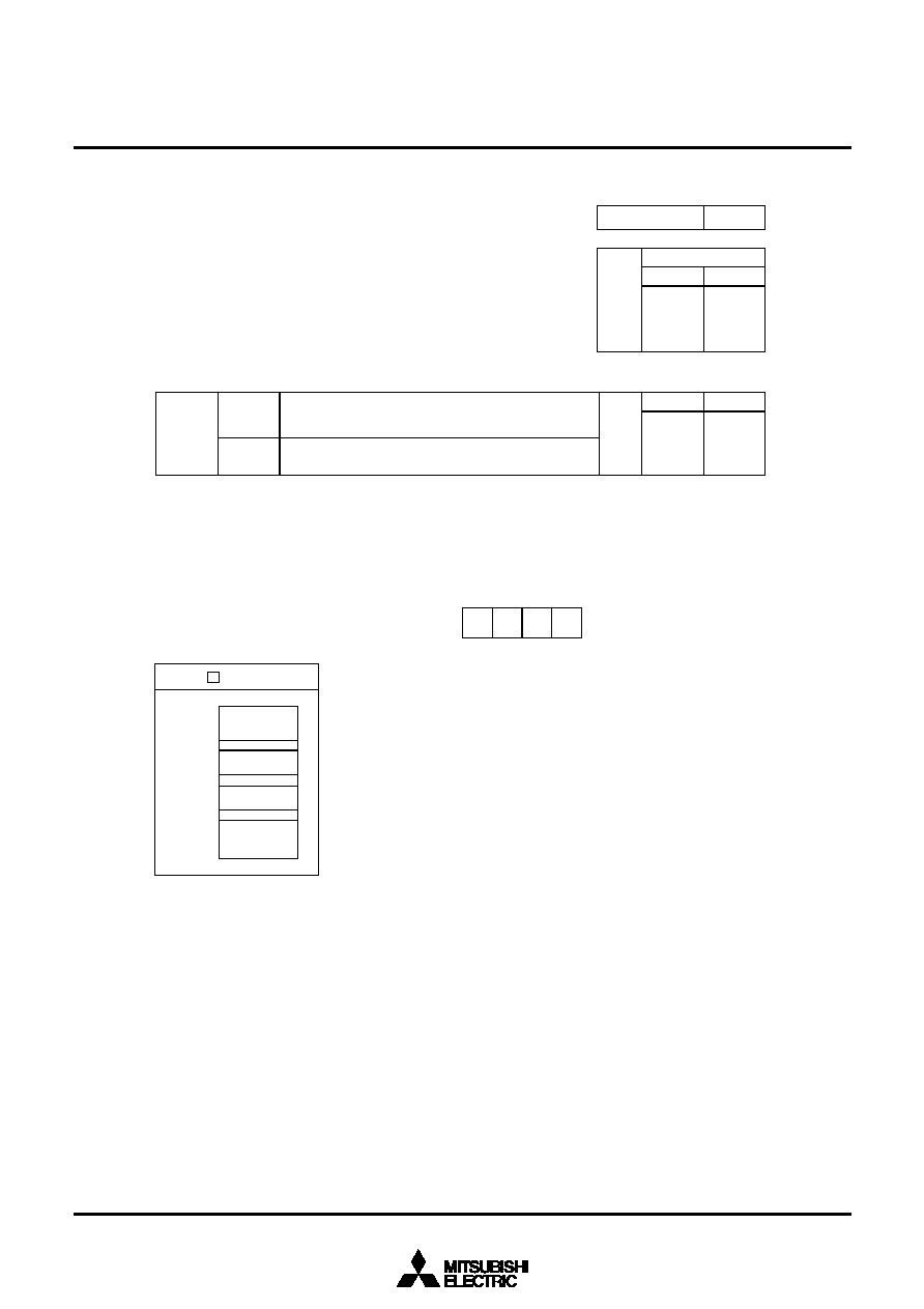
MITSUBISHI MICROCOMPUTERS
M37210M3-XXXSP/FP, M37210M4-XXXSP, M37211M2-XXXSP
M37210E4-XXXSP/FP, M37210E4SP/FP
SINGLE-CHIP 8-BIT CMOS MICROCOMPUTER for VOLTAGE SYNTHESIZER
with ON-SCREEN DISPLAY CONTROLLER
50
GZZSH0610B < 25B0 >
740 FAMILY MASK ROM CONFIRMATION FORM
SINGLE-CHIP MICROCOMPUTER M37210M4-XXXSP
MITSUBISHI ELECTRIC
Mask ROM number
Date :
Supervisor
signature
Receipt
Section head
signature
g
Customer
Company
name
Date
issued
Date :
TEL
( )
Note : Please fill in all items marked
g
.
Submitted by
Supervisor
Issuance
signature
g
1. Confirmation
Specify the name of the product being ordered and the type of EPROMs submitted.
Three EPROMs are required for each pattern.
If at least two of the three sets of EPROMs submitted contain identical data, we will produce masks based on
this data. We shall assume the responsibility for errors only if the mask ROM data on the products we produce
differs from this data. Thus, extreme care must be taken to verify the data in the submitted EPROMs.
Checksum code for entire EPROM
(hexadecimal notation)
27256
EPROM address
0000
16
Product name
ASCII code :
`M37210M4 '
ROM (16K bytes)
000F
16
15FF
16
1800
16
1DFF
16
Set "FF
16
" in the shaded area.
Write the ASCII codes that indicates the product name of "M37210M4" to addresses 0000
16
to 000F
16
.
(1)
(2)
EPROM type (indicate the type used)
1000
16
Character ROM1
4000
16
7FFF
16
Character ROM2
g
2. Mark specification
Mark specification must be submitted using the correct form for the type package being ordered fill out the appropriate
mark specification form (52P4B for M37210M4-XXXSP) and attach to the mask ROM confirmation form.
g
3. Comments
(1/3)
MITSUBISHI MICROCOMPUTERS
M37210M3-XXXSP/FP, M37210M4-XXXSP, M37211M2-XXXSP
M37210E4-XXXSP/FP, M37210E4SP/FP
SINGLE-CHIP 8-BIT CMOS MICROCOMPUTER for VOLTAGE SYNTHESIZER
with ON-SCREEN DISPLAY CONTROLLER
51
GZZSH0610B < 25B0 >
740 FAMILY MASK ROM CONFIRMATION FORM
SINGLE-CHIP MICROCOMPUTER M37210M4-XXXSP
MITSUBISHI ELECTRIC
`M' =
16
4 D
16
`3' = 3 3
16
`7' = 3 7
16
`2' = 3 2
16
`1' = 3 1
16
`0' = 3 0
16
`M' = 4 D
16
`4' = 3 4
0000
16
0001
16
0002
16
0003
16
0004
16
0005
16
0006
16
0007
16
Address
`' =
16
2 D
16
F F
16
F F
16
F F
16
F F
16
F F
16
F F
16
F F
0008
16
0009
16
000A
16
000B
16
000C
16
000D
16
000E
16
000F
16
Address
Addresses 0000
16
to 000F
16
store the product name, and addresses 1000
16
to 15FF
16
and addresses 1800
16
to 1DFF
16
store the character pattern.
If the name of the product contained in the EPROMs does not match the name on the mask ROM confirmation form, the
ROM processing is disabled. Write the data correctly.
Inputting the name of the product with the ASCII code
ASCII codes `M37210M4-' are listed on the right.
The addresses and data are in hexadecimal notation.
1.
Inputting the character ROM
Input the character ROM data by dividing it into character ROM1 and character ROM2. For the character ROM data,
see the next page and on.
2.
Writing the product name and character ROM data onto EPROMs
(2/3)
MITSUBISHI MICROCOMPUTERS
M37210M3-XXXSP/FP, M37210M4-XXXSP, M37211M2-XXXSP
M37210E4-XXXSP/FP, M37210E4SP/FP
SINGLE-CHIP 8-BIT CMOS MICROCOMPUTER for VOLTAGE SYNTHESIZER
with ON-SCREEN DISPLAY CONTROLLER
52
GZZSH0610B < 25B0 >
740 FAMILY MASK ROM CONFIRMATION FORM
SINGLE-CHIP MICROCOMPUTER M37210M4-XXXSP
MITSUBISHI ELECTRIC
The structure of character ROM (divided of 12
!
16 dots font)
Example
Character code
"1A
16
"
Example
11A0
16
to
11AF
16
b
7
b
6
b
5
b
4
b
3
b
2
b
1
b
0
b
7
b
6
b
5
b
4
b
3
b
2
b
1
b
0
0
1
2
3
4
5
6
7
8
9
A
B
C
D
E
F
0
1
2
3
4
5
6
7
8
9
A
B
C
D
E
F
00
16
04
16
04
16
0A
16
0A
16
11
16
11
16
11
16
20
16
20
16
3F
16
40
16
40
16
40
16
00
16
00
16
F0
16
F0
16
F0
16
F0
16
F0
16
F0
16
F0
16
F0
16
F8
16
F8
16
F8
16
F4
16
F4
16
F4
16
F0
16
F0
16
Example
19A0
16
to
19AF
16
Character
ROM1
Character
ROM2
F
16
(3/3)

MITSUBISHI MICROCOMPUTERS
M37210M3-XXXSP/FP, M37210M4-XXXSP, M37211M2-XXXSP
M37210E4-XXXSP/FP, M37210E4SP/FP
SINGLE-CHIP 8-BIT CMOS MICROCOMPUTER for VOLTAGE SYNTHESIZER
with ON-SCREEN DISPLAY CONTROLLER
53
GZZSH0611B < 25B1 >
740 FAMILY MASK ROM CONFIRMATION FORM
SINGLE-CHIP MICROCOMPUTER M37211M2-XXXSP
MITSUBISHI ELECTRIC
Mask ROM number
Date :
Supervisor
signature
Receipt
Section head
signature
g
Customer
Company
name
Date
issued
Date :
TEL
( )
Note : Please fill in all items marked
g
.
Submitted by
Supervisor
Issuance
signature
g
1. Confirmation
Specify the name of the product being ordered and the type of EPROMs submitted.
Three EPROMs are required for each pattern.
If at least two of the three sets of EPROMs submitted contain identical data, we will produce masks based on
this data. We shall assume the responsibility for errors only if the mask ROM data on the products we produce
differs from this data. Thus, extreme care must be taken to verify the data in the submitted EPROMs.
Checksum code for entire EPROM
(hexadecimal notation)
27256
EPROM address
0000
16
Product name
ASCII code :
`M37211M2 '
ROM (8K bytes)
000F
16
15FF
16
1800
16
1DFF
16
Set "FF
16
" in the shaded area.
Write the ASCII codes that indicates the product name of "M37211M2" to addresses 0000
16
to 000F
16
.
(1)
(2)
EPROM type (indicate the type used)
1000
16
Character ROM1
6000
16
7FFF
16
Character ROM2
g
2. Mark specification
Mark specification must be submitted using the correct form for the type package being ordered fill out the appropriate
mark specification form (52P4B for M37211M2-XXXSP) and attach to the mask ROM confirmation form.
g
3. Note
Set the stack page selection bit to "0", because this bit is set to "1" after reset but the internal RAM is located at 0
page only.
Both P0
2
pin (9th pin) and P0
3
pin (10th pin) are not used as PWM output pins.
(1)
(2)
g
4. Comments
(1/3)
MITSUBISHI MICROCOMPUTERS
M37210M3-XXXSP/FP, M37210M4-XXXSP, M37211M2-XXXSP
M37210E4-XXXSP/FP, M37210E4SP/FP
SINGLE-CHIP 8-BIT CMOS MICROCOMPUTER for VOLTAGE SYNTHESIZER
with ON-SCREEN DISPLAY CONTROLLER
54
GZZSH0611B< 25B1 >
740 FAMILY MASK ROM CONFIRMATION FORM
SINGLE-CHIP MICROCOMPUTER M37211M2-XXXSP
MITSUBISHI ELECTRIC
`M' =
16
4 D
16
`3' = 3 3
16
`7' = 3 7
16
`2' = 3 2
16
`1' = 3
1
16
`1' = 3 1
16
`M' = 4 D
16
`2' = 3 2
0000
16
0001
16
0002
16
0003
16
0004
16
0005
16
0006
16
0007
16
Address
`' =
16
2 D
16
F F
16
F F
16
F F
16
F F
16
F F
16
F F
16
F F
0008
16
0009
16
000A
16
000B
16
000C
16
000D
16
000E
16
000F
16
Address
Addresses 0000
16
to 000F
16
store the product name, and addresses 1000
16
to 15FF
16
and addresses 1800
16
to 1DFF
16
store the character pattern.
If the name of the product contained in the EPROMs does not match the name on the mask ROM confirmation form, the
ROM processing is disabled. Write the data correctly.
Inputting the name of the product with the ASCII code
ASCII codes `M37211M2-' are listed on the right.
The addresses and data are in hexadecimal notation.
1.
Inputting the character ROM
Input the character ROM data by dividing it into character ROM1 and character ROM2. For the character ROM data,
see the next page and on.
2.
Writing the product name and character ROM data onto EPROMs
(2/3)

MITSUBISHI MICROCOMPUTERS
M37210M3-XXXSP/FP, M37210M4-XXXSP, M37211M2-XXXSP
M37210E4-XXXSP/FP, M37210E4SP/FP
SINGLE-CHIP 8-BIT CMOS MICROCOMPUTER for VOLTAGE SYNTHESIZER
with ON-SCREEN DISPLAY CONTROLLER
55
GZZSH0611B < 25B1 >
740 FAMILY MASK ROM CONFIRMATION FORM
SINGLE-CHIP MICROCOMPUTER M37211M2-XXXSP
MITSUBISHI ELECTRIC
The structure of character ROM (divided of 12
!
16 dots font)
Example
Character code
"1A
16
"
Example
11A0
16
to
11AF
16
b
7
b
6
b
5
b
4
b
3
b
2
b
1
b
0
b
7
b
6
b
5
b
4
b
3
b
2
b
1
b
0
0
1
2
3
4
5
6
7
8
9
A
B
C
D
E
F
0
1
2
3
4
5
6
7
8
9
A
B
C
D
E
F
00
16
04
16
04
16
0A
16
0A
16
11
16
11
16
11
16
20
16
20
16
3F
16
40
16
40
16
40
16
00
16
00
16
F0
16
F0
16
F0
16
F0
16
F0
16
F0
16
F0
16
F0
16
F8
16
F8
16
F8
16
F4
16
F4
16
F4
16
F0
16
F0
16
Example
19A0
16
to
19AF
16
Character
ROM1
Character
ROM2
F
16
(3/3)
MITSUBISHI MICROCOMPUTERS
M37210M3-XXXSP/FP, M37210M4-XXXSP, M37211M2-XXXSP
M37210E4-XXXSP/FP, M37210E4SP/FP
SINGLE-CHIP 8-BIT CMOS MICROCOMPUTER for VOLTAGE SYNTHESIZER
with ON-SCREEN DISPLAY CONTROLLER
56
MITSUBISHI MICROCOMPUTERS
M37210M3-XXXSP/FP, M37210M4-XXXSP, M37211M2-XXXSP
M37210E4-XXXSP/FP, M37210E4SP/FP
SINGLE-CHIP 8-BIT CMOS MICROCOMPUTER for VOLTAGE SYNTHESIZER
with ON-SCREEN DISPLAY CONTROLLER
57

Sep. First Edition 1996 H-DF319-B
Editioned by
Committee of editing of Mitsubishi Semiconductor Data Book
Published by
Mitsubishi Electric Corp., Semiconductor Division
This book, or parts thereof, may not be reproduced in any form without permission of
Mitsubishi Electric Corporation.
MITSUBISHI DATA BOOK
SINGLE-CHIP 8-BIT MICROCOMPUTERS Vol.3
Rev.
Rev.
No.
date
1.0
First Edition 9708
2.0
Information about copyright note, revision number, release date added (last page).
971130
M37210M3-XXXSP/FP, M37210M4-XXXSP, M37211M2-XXXSP,
M37210E4-XXXSP/FP, M37210E4SP/FP
DATA SHEET
Revision Description
REVISION DESCRIPTION LIST
(1/1)
Document Outline