
1
2
3
4
5
6
7
8
9
10
11
12
13
14
15
16
17
18
19
20
21
42
41
40
39
38
37
36
35
34
33
32
31
30
29
28
27
26
25
24
23
22
P0
6
/INT2/A-D4
X
OUT
H
SYNC
V
SYNC
P0
0
/PWM0
P0
1
/PWM1
P0
2
/PWM2
P0
3
/PWM3
P0
4
/PWM4
P0
5
/PWM5
P0
7
/INT1
P2
3
/TIM3
P2
4
/TIM2
P2
5
P2
6
P2
7
D-A
P3
2
CNV
SS
X
IN
V
SS
P5
2
/R
P5
3
/G
P5
4
/B
P5
5
/OUT
P2
0
/S
CLK
P2
1
/S
OUT
P2
2
/S
IN
P1
0
P1
1
P1
2
P1
3
P1
4
P1
5
/A-D1/INT3
P1
6
/A-D2
P3
0
/A-D5/DA1
P3
1
/A-D6/DA2
RESET
OSC1/P3
3
OSC2/P3
4
V
CC
P1
7
/A-D3
M37220M3-XXXSP
PIN CONFIGURATION (TOP VIEW)
DESCRIPTION
The M37220M3-XXXSP is a single-chip microcomputer designed with
CMOS silicon gate technology. It is housed in a 42-pin shrink plastic
molded DIP.
In addition to their simple instruction sets, the ROM, RAM and I/O
addresses are placed on the same memory map to enable easy pro-
gramming.
The M37220M3-XXXSP has a PWM output function and a OSD dis-
play function, so it is useful for a channel selection system for TV.
FEATURES
∑
Number of basic instructions ..................................................... 71
∑
Memory size
ROM ........................................................ 12 K bytes
RAM ......................................................... 256 bytes
ROM for display......................................... 4 K bytes
RAM for display .......................................... 80 bytes
∑
The minimum instruction execution time
.......................................... 0.5
µ
s (at 8 MHz oscillation frequency)
∑
Power source voltage .................................................. 5 V
±
10 %
∑
Power dissipation ............................................................. 165 mW
(at 8 MHz oscillation frequency, V
CC
=5.5V, at CRT display)
∑
Subroutine nesting ....................................... 96 levels (maximum)
∑
Interrupts ....................................................... 13 types, 13 vectors
∑
8-bit timers .................................................................................. 4
∑
Programmable I/O ports (Ports P0, P1, P2, P3
0
≠P3
2
) .............. 27
∑
Input ports (Ports P3
3
, P3
4
) ......................................................... 2
∑
Output ports (Ports P5
2
≠P5
5
) ...................................................... 4
∑
12 V withstand ports .................................................................... 6
∑
LED drive ports ........................................................................... 4
∑
Serial I/O ............................................................ 8-bit
!
1 channel
∑
A-D comparator (6-bit resolution) ................................ 6 channels
∑
D-A converter (6-bit resolution) ................................................... 2
∑
PWM output circuit ......................................... 14-bit
!
1, 8-bit
!
6
∑
CRT display function
Number of display characters ................ 24 characters
!
2 lines
(16 lines maximum)
Kinds of characters ..................................................... 128 kinds
Dot structure .......................................................... 12
!
16 dots
Kinds of character sizes .................................................. 3 kinds
Kinds of character colors (It can be specified by the character)
maximum 7 kinds (R, G, B)
Kinds of raster colors (maximum 7 kinds)
Display position
Horizontal .................................................................. 64 levels
Vertical .................................................................... 128 levels
Bordering (horizontal and vertical)
APPLICATION
TV
Outline 42P4B
MITSUBISHI MICROCOMPUTERS
M37220M3-XXXSP
SINGLE-CHIP 8-BIT CMOS MICROCOMPUTER for VOLTAGE SYNTHESIZER
with ON-SCREEN DISPLAY CONTROLLER
MITSUBISHI MICROCOMPUTERS
M37220M3-XXXSP
SINGLE-CHIP 8-BIT CMOS MICROCOMPUTER for VOLTAGE SYNTHESIZER
with ON-SCREEN DISPLAY CONTROLLER
2
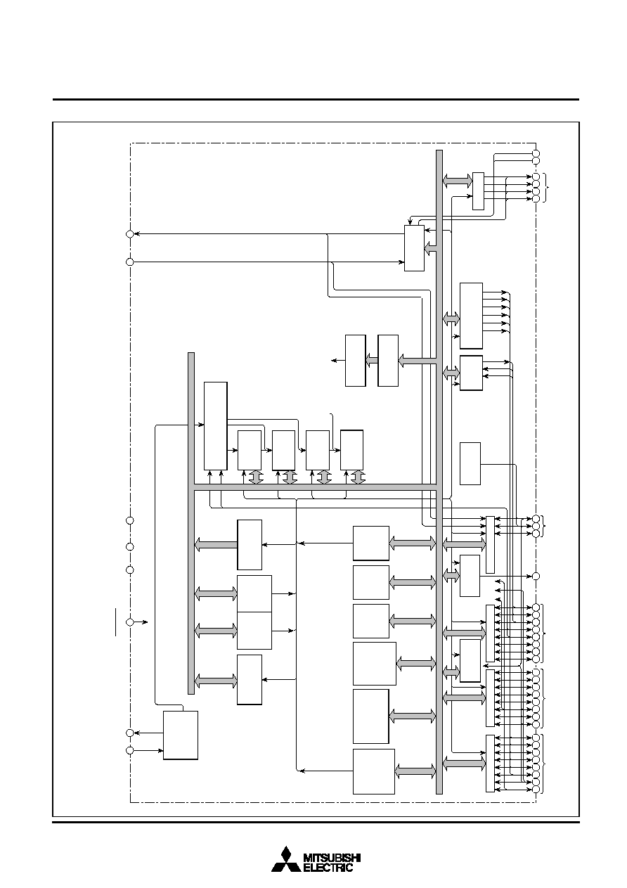
FUNCTIONAL BLOCK DIAGRAM of M37220M3-XXXSP
OUT
Clock input
Clock output
X
IN
X
OUT
Reset input
V
CC
V
SS
CNV
SS
Clock output for display
Input ports P3
3,
P3
4
OSC1
OSC2
Clock input for display
INT2
INT1
PWM5
PWM4
PWM3
PWM2
PWM1
PWM0
P5 (4)
B
G
R
H
SYNC
V
SYNC
A-D
comparator
14-bit
PWM circuit
8-bit PWM circuit
Accumulator
A (8)
Timer 4
T4 (8)
Timer 3
T3 (8)
Timer 2
T2 (8)
Timer 1
T1 (8)
Timer count source
selection circuit
TIM2
TIM3
Instruction
register (8)
Instruction
decoder
Control signal
CRT circuit
Stack
pointer
S (8)
Index
register
Y (8)
Index
register
X (8)
Processor
status
register
PS (8)
8-bit
arithmetic
and
logical unit
ROM
12 K bytes
Program
counter
PC
L
(8)
Program
counter
PC
H
(8)
RAM
256 bytes
Data bus
Clock
generating
circuit
RESET
Output ports P5
2
≠P5
5
Address bus
SI/O(8)
S
IN
S
CLK
S
OUT
INT3
10
9
8
7
6
5
4
3
I/O port P0
28
29
30
31
32
33
34
35
P1
(
8
)
I/O port P1
15
14
13
12
11
36
37
38
P2
(
8
)
I/O port P2
I/O ports P3
0
≠P3
2
17
26
27
16
P3
(
3
)
P0
(
8
)
39
40
41
42
2
1
20
19
25
22
21
18
24
23
(
) Timing output
D-
A
D-A
converter

MITSUBISHI MICROCOMPUTERS
M37220M3-XXXSP
SINGLE-CHIP 8-BIT CMOS MICROCOMPUTER for VOLTAGE SYNTHESIZER
with ON-SCREEN DISPLAY CONTROLLER
3
Number of basic instructions
Instruction execution time
Clock frequency
Memory size
Input/Output ports
Serial I/O
A-D comparatpr
D-A converter
PWM output circuit
Timers
Subroutine nesting
Interrupt
Clock generating circuit
Power source voltage
Power dissipation
Operating temperature range
Device structure
Package
CRT display function
71
0.5
µ
s (the minimum instruction execution time, at 8 MHz oscillation fre-
quency)
8 MHz (maximum)
12K bytes
256 bytes
4K bytes
80 bytes
8-bit
!
1 (N-channel open-drain output structure, can be used as PWM
output pins, INT input pins, A-D input pin)
8-bit
!
1 (CMOS input/output structure, can be used as A-D input pins, INT
input pin)
2-bit
!
1 (CMOS input/output or N-channel open-drain output structure,
can be used as serial output pins)
6-bit
!
1 (CMOS input/output structure, can be used as serial input pin,
external clock input pins)
2-bit
!
1 (CMOS input/output or N-channel open-drain output structure,
can be used as A-D input pins, D-A conversion output pins)
1-bit
!
1 (N-channel open-drain output structure)
2-bit
!
1 (can be used as CRT display clock I/O pins)
4-bit
!
1 (CMOS output structure, can be used as CRT output pins)
8-bit
!
1
6 channels (6-bit resolution)
2 (6-bit resolution)
14-bit
!
1, 8-bit
!
6
8-bit timer
!
4
96 levels (maximum)
External interrupt
!
3, Internal timer interrupt
!
4, Serial I/O interrupt
!
1,
CRT interrupt
!
1, X
IN
/4096 interrupt
!
1, V
SYNC
interrupt
!
1,
BRK interrupt
!
1
2 built-in circuits (externally connected a ceramic resonator or a quartz-
crystal oscillator)
5 V
±
10 %
165 mW typ. (at oscillation frequency f
CPU
= 8 MHz, f
CRT
= 8 MHz)
110 mW typ. (at oscillation frequency f
CPU
= 8 MHz)
1.65 mW (maximum)
≠10
∞
C to 70
∞
C
CMOS silicon gate process
42-pin shrink plastic molded DIP
20 characters
!
2 lines (maximum 16 lines by software)
12
!
16 dots
128 kinds
3 kinds
Maximum 7 kinds (R, G, B); can be specified by the character
64 levels (horizontal)
!
128 levels (vertical)
Parameter
Functions
FUNCTIONS
ROM
RAM
CRT ROM
CRT RAM
P0
P1
0
≠P1
7
P2
0
, P2
1
P2
2
≠P2
7
P3
0
, P3
1
P3
2
P3
3
, P3
4
P5
2
≠P5
5
I/O
I/O
I/O
I/O
I/O
I/O
Input
Output
CRT ON
CRT OFF
In stop mode
Number of display characters
Dot structure
Kinds of characters
Kinds of character sizes
Kinds of character colors
Display position (horizontal, vertical)

MITSUBISHI MICROCOMPUTERS
M37220M3-XXXSP
SINGLE-CHIP 8-BIT CMOS MICROCOMPUTER for VOLTAGE SYNTHESIZER
with ON-SCREEN DISPLAY CONTROLLER
4
PIN DESCRIPTION
Pin
Input/
Output
Name
V
CC,
V
SS
CNV
SS
RESET
X
IN
X
OUT
P0
0
/PWM0≠
P0
5
/PWM5,
P0
6
/INT2/
A-D4,
P0
7
/INT1
P1
0
≠P1
4
,
P1
5
/A-D1
INT3,
P1
6
/A-D2,
P1
7
/A-D3
P2
0
/S
CLK
,
P2
1
/S
OUT
,
P2
2
/S
IN
,
P2
3
/TIM3,
P2
4
/TIM2,
P2
5
≠P2
7
P3
0
/A-D5/
DA1,
P3
1
/A-D6/
DA2,
P3
2
P3
3
/OSC1,
P3
4
/OSC2
Apply voltage of 5 V
±
10 % (typical) to V
CC
, and 0 V to V
SS
.
This is connected to V
SS
.
To enter the reset state, the reset input pin must be kept at a "L" for 2
µ
s or more (under
normal V
CC
conditions).
If more time is needed for the quartz-crystal oscillator to stabilize, this "L" condition should
be maintained for the required time.
This chip has an internal clock generating circuit. To control generating frequency, an
external ceramic resonator or a quartz-crystal oscillator is connected between pins X
IN
and
X
OUT
. If an external clock is used, the clock source should be connected to the X
IN
pin and
the X
OUT
pin should be left open.
Port P0 is an 8-bit I/O port with direction register allowing each I/O bit to be individually
programmed as input or output. At reset, this port is set to input mode. The output structure
is N-channel open-drain output. The note out of this Table gives a full of port P0 function.
Pins P0
0
≠P0
5
are also used as PWM output pins PWM0≠PWM5 respectively.The output
structure is N-channel open-drain output.
Pins P0
6
, P0
7
are also used as external interrupt input pins INT2, INT1 respectively.
Pins P0
6
is also used as an analog interrupt input pin A-D4.
Port P1 is an 8-bit I/O port and has basically the same functions as port P0. The output
structure is CMOS output.
Pins P1
5
≠P1
7
are also used as an analog input pins A-D1 to A-D3.
Pin P1
5
is also used as an external interrupt input pins INT3.
Port P2 is an 8-bit I/O port and has basically the same functions as port P0. The output
structure is CMOS output.
Pins P2
3
, P2
4
is also used an external clock input pins TIM3, TIM2 respectively.
Pins P2
1
, P2
2
are also used serial I/O data input/output pins S
OUT
, S
IN
respectively. The
output structure is N-channel open-drain output.
Pin P2
0
is also used serial I/O syncronizing clock input/output pin S
CLK
. The output struc-
ture is N-channel open-drain output.
Ports P3
0
≠P3
2
are a 3-bit I/O port and have basically the same functions as port P0. Either
CMOS output or N-channel open-drain output structure can be selected as the ports P3
0
and P3
1
. The output structure of port P3
2
is N-channel open-drain output.
Pins P3
0
, P3
1
are also used as analog input pins A-D5, A-D6 respectively.
Pins P3
0
, P3
1
are also used as D-A conversion output pins DA1, DA2 respectively.
Ports P3
3
, P3
4
are a 2-bit input port.
Pin P3
3
is also used as CRT display clock input pin OSC1.
Pin P3
4
is also used as CRT display clock output pin OSC2.The output structure is CMOS
output.
Input
Input
Output
I/O
Output
Input
Input
I/O
Input
Input
I/O
Input
I/O
I/O
I/O
Input
Output
Input
Input
Output
Power source
CNV
SS
Reset input
Clock input
Clock output
I/O port P0
PWM output
External interrupt
input
Analog input
I/O port P1
Analog input
External interrupt
input
I/O port P2
External clock
input
Serial I/O data
input/output
Serial I/O synchro-
nizing clock input/
output
I/O port P3
Analog input
D-A conversion
output
Input port P3
Clock input for
CRT display
Clock output for
CRT display
Functions

MITSUBISHI MICROCOMPUTERS
M37220M3-XXXSP
SINGLE-CHIP 8-BIT CMOS MICROCOMPUTER for VOLTAGE SYNTHESIZER
with ON-SCREEN DISPLAY CONTROLLER
5
Output port
P5
CRT output
H
SYNC
input
V
SYNC
input
DA output
PIN DESCRIPTION (continued)
P5
2
/R,
P5
3
/G,
P5
4
/B,
P5
5
/OUT
H
SYNC
V
SYNC
D-A
Output
Output
Input
Input
Output
Ports P5
2
≠P5
5
are a 4-bit output port. The output structure is CMOS output.
Pins P5
2
≠P5
5
are also used as CRT output pins R, G, B, OUT respectively. The output structure is
CMOS output.
This is a horizontal synchronizing signal input for CRT display.
This is a vertical synchronizing signal input for CRT display.
This is an output pin for 14-bit PWM.
Note : As shown in the memory map (Figure 3), port P0 is accessed as a memory at address 00C0
16
of zero page. Port P0 has the port P0
direction register (address 00C1
16
of zero page) which can be used to program each bit as an input ("0") or an output ("1"). The pins
programmed as "1" in the direction register are output pins. When pins are programmed as "0," they are input pins. When pins are
programmed as output pins, the output data are written into the port latch and then output. When data is read from the output pins, the
output pin level is not read but the data of the port latch is read. This allows a previously-output value to be read correctly even if the
output "L" voltage has risen, for example, because a light emitting diode was directly driven. The input pins are in the floating state, so the
values of the pins can be read. When data is written into the input pin, it is written only into the port latch, while the pin remains in the
floating state.