 | ÐлекÑÑоннÑй компоненÑ: M37225M6 | СкаÑаÑÑ:  PDF PDF  ZIP ZIP |
Äîêóìåíòàöèÿ è îïèñàíèÿ www.docs.chipfind.ru

1. DESCRIPTION
The M37225M6-XXXSP, M37225M8-XXXSP, and M37225ECSP are
single-chip microcomputers designed with CMOS silicon gate tech-
nology. They have a OSD, I
2
C-BUS interface, PWM output, and 12 V
withstand, so it is useful for a channel selection system for TV.
The features of the M37225ECSP are similar to those of the
M37225M6-XXXSP except that the chip has a built-in PROM which
can be written electrically. The difference between M37225M6-XXXSP
and M37225M8-XXXSP are the ROM size. Accordingly, the follow-
ing descriptions will be for the M37225M6-XXXSP.
2. FEATURES
q
Number of basic instructions .................................................... 71
q
Memory size
ROM ..................... 24K bytes (M37225M6-XXXSP)
32K bytes (M37225M8-XXXSP)
48K bytes (M37225ECSP)
RAM ...................... 1024 bytes (M37225M6-XXXSP,
M37225M8-XXXSP)
2048 bytes (M37225ECSP)
(*ROM correction memory included)
q
Minimum instruction execution time
......................................... 0.5
µ
s
(at 8 MHz oscillation frequency)
q
Power source voltage ................................................. 5 V
±
10 %
q
Subroutine nesting ............................................. 128 levels (Max.)
q
Interrupts ....................................................... 16 types, 16 vectors
q
8-bit timers .................................................................................. 4
q
Programmable I/O ports (Ports P0, P1, P2, P3
0
P3
2
, P3
5
) ..... 28
q
Input ports (Ports P3
3
, P3
4
, P5
0
, P5
1
) ........................................ 4
q
Output ports (Ports P5
2
P5
5
) ..................................................... 4
q
12 V withstand ports ................................................................... 6
q
LED drive ports ........................................................................... 4
q
Serial I/O ............................................................ 8-bit
!
1 channel
q
Multi-master I
2
C-BUS interface .............................. 1 (2 systems)
q
A-D converter (8-bit resolution) .................................... 8 channels
q
PWM output circuit ........................................ 14-bit
!
2, 8-bit
!
6
q
Power dissipation
In operating ...................................................................... 165 mW
(at V
CC
= 5.5V, 8 MHz oscillation frequency, and OSD on)
q
ROM correction function ................................................ 3 vectors
q
Immediate return mode from wait state
SINGLE-CHIP 8-BIT CMOS MICROCOMPUTER for VOLTAGE SYNTHESIZER
with ON-SCREEN DISPLAY CONTROLLER
M37225M6-XXXSP, M37225M8-XXXSP
M37225ECSP
MITSUBISHI MICROCOMPUTERS
q
OSD function
Display characters ............................................... 24 characters
!
2 lines
(It is possible to display 3 lines or more by software)
Kinds of characters ......... 381 kinds
Character display area
16
!
20 dots
Kinds of character sizes .............................. Block display: 3 kinds
SPRITE display: 1 kinds
Kinds of character colors. ................................. 8 colors (R, G, B)
Coloring unit ................... character, character background, raster
Display position
Horizontal: 64 levels
Vertical :255 levels
Attribute ........ Border (all-bordered, shadow-bordered), BUTTON
SPRITE display function
Wallpaper function
Window function
Corresponding to bi-scan mode
3. APPLICATION
TV
Rev. 1.1

2
SINGLE-CHIP 8-BIT CMOS MICROCOMPUTER for VOLTAGE SYNTHESIZER
with ON-SCREEN DISPLAY CONTROLLER
M37225M6XXXSP, M37225M8XXXSP
M37225ECSP
MITSUBISHI MICROCOMPUTERS
Rev. 1.0
TABLE OF CONTENTS
1. DESCRIPTION .......................................................................... 1
2. FEAUTURES ............................................................................. 1
3. APPLICATION ............................................................................ 1
4. PIN CONFIGURATION .............................................................. 3
5. FUNCTIONAL BLOCK DIAGRAM ............................................. 4
6. PERFORMANCE OVERVIEW ................................................... 5
7. PIN DESCRIPTION ................................................................... 7
8. FUNCTIONAL DESCRIPTION ................................................. 11
8.1 CENTRAL PROCESSING UNIT (CPU) .................... 11
8.2 MEMORY .................................................................. 12
8.3 INTERRUPTS ........................................................... 19
8.4 TIMERS ..................................................................... 24
8.5 SERIAL I/O ................................................................ 27
8.6 MULTI-MASTER I
2
C-BUS INTERFACE .................... 31
8.7 PWM OUTPUT CIRCUIT .......................................... 44
8.8 A-D COMPARATOR .................................................. 49
8.9 ROM CORRECTION FUNCTION ............................. 53
8.10 OSD FUNCTIONS ................................................... 54
(1) Clock for OSD .................................................... 57
(2) Scan mode ......................................................... 58
(3) OSD input/output pin control .............................. 59
8.10.1 Block Display .................................................... 60
(1) Display position .................................................. 61
(2) Dot size .............................................................. 65
(3) Memory For OSD ............................................... 66
(4) Character Color .................................................. 69
(5) Character Background Color .............................. 69
(6) OUT1, OUT2 Signals ......................................... 69
(7) Attribute .............................................................. 72
(8) Multiple Display .................................................. 76
(9) Window Function ................................................ 77
8.10.2 SPRITE Display ................................................ 80
8.10.3 Raster Display ................................................... 83
8.11. SOFTWARE RUNAWAY DETECT FUNCTION ...... 85
8.12. RESET CIRCUIT .................................................... 86
8.13. CLOCK GENERATING CIRCUIT ........................... 87
8.14. DISPLAY OSCILLATION CIRCUIT ........................ 88
8.15. AUTO-CLEAR CIRCUIT ......................................... 88
8.16. ADDRESSING MODE ............................................ 88
8.17. MACHINE INSTRUCTIONS ................................... 88
9. PROGRAMMING NOTES ........................................................ 88
10. ABSOLUTE MAXIMUM RATINGS ......................................... 89
11. RECOMMENDED OPERATING CONDITIONS ..................... 89
12. ELECTRIC CHARACTERISTICS .......................................... 90
13. A-D COMPARISON CHARACTERISTICS ............................. 92
14. MULTI-MASTER I
2
C-BUS BUS LINE CHARACTERISTICS ........... 92
15. PROM PROGRAMMING METHOD ....................................... 93
16. DATA REQUIRED FOR MASK ORDERS .............................. 94
17. MASK CONFIRMATION FORM ............................................. 95
18. MARK SPECIFICATION FORM ........................................... 101
19. ONE TIME PROM VERSIONS M37225ECSP MARKING ... 102
20. APPENDIX ........................................................................... 103
21. PACKAGE OUTLINE ........................................................... 131
3
SINGLE-CHIP 8-BIT CMOS MICROCOMPUTER for VOLTAGE SYNTHESIZER
with ON-SCREEN DISPLAY CONTROLLER
M37225M6XXXSP, M37225M8XXXSP
M37225ECSP
MITSUBISHI MICROCOMPUTERS
Rev. 1.0
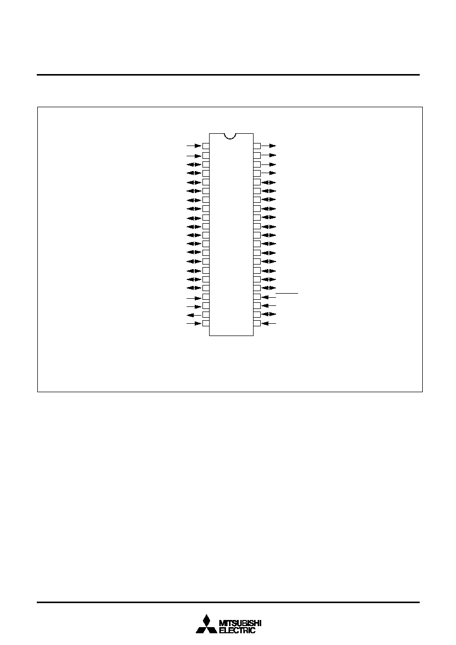
4. PIN CONFIGURATION
Outline 42P4B
Fig. 4.1 Pin Configuration (Top View)
P
0
6
/
I
N
T
2
/
A
-
D
4
X
O
U
T
H
S
Y
N
C
/
P
5
0
V
S
Y
N
C
/
P
5
1
P
0
0
/
P
W
M
0
P
0
1
/
P
W
M
1
P
0
2
/
P
W
M
2
P
0
3
/
P
W
M
3
P
0
4
/
P
W
M
4
P
0
5
/
P
W
M
5
P
0
7
/
I
N
T
1
P
2
3
/
T
I
M
3
P
2
4
/
T
I
M
2
P
2
5
P
2
6
P
2
7
D
A
1
/
P
3
5
P
3
2
/
A
-
D
7
C
N
V
S
S
X
I
N
V
S
S
1
2
3
4
5
6
7
8
9
1
0
1
1
1
2
1
3
1
4
1
5
1
6
1
7
1
8
1
9
2
0
2
1
4
2
4
1
4
0
3
9
3
8
3
7
3
6
3
5
3
4
3
3
3
2
3
1
3
0
2
9
2
8
2
7
2
6
2
5
2
4
2
3
2
2
R
E
S
E
T
R
/
P
5
2
G
/
P
5
3
B
/
P
5
4
O
U
T
1
/
P
5
5
P
2
0
/
S
C
L
K
P
2
1
/
S
O
U
T
(
/S
I
N
)
P
2
2
/
S
I
N
P
1
0
/
OU
T
2
/
A
-
D
8
P
1
1
/
S
C
L
1
P
1
2
/
S
C
L
2
P
1
3
/
S
D
A
1
P
1
4
/
S
D
A
2
P
1
6
/
A
-
D
2
P
3
0
/
A
-
D
5
P
3
1
/
A
-
D
6
O
S
C
1
/
P
3
3
O
S
C
2
/
P
3
4
V
C
C
P
1
7
/
D
A
2
/A
-
D3
P
1
5
/
I
N
T
3
/
A
-
D
1
M
3
7
2
2
5
M
6
-
X
X
X
S
P
M
3
7
2
2
5
M
8
-
X
X
X
S
P
M
3
7
2
2
5
E
C
S
P
4
SINGLE-CHIP 8-BIT CMOS MICROCOMPUTER for VOLTAGE SYNTHESIZER
with ON-SCREEN DISPLAY CONTROLLER
M37225M6XXXSP, M37225M8XXXSP
M37225ECSP
MITSUBISHI MICROCOMPUTERS
Rev. 1.0
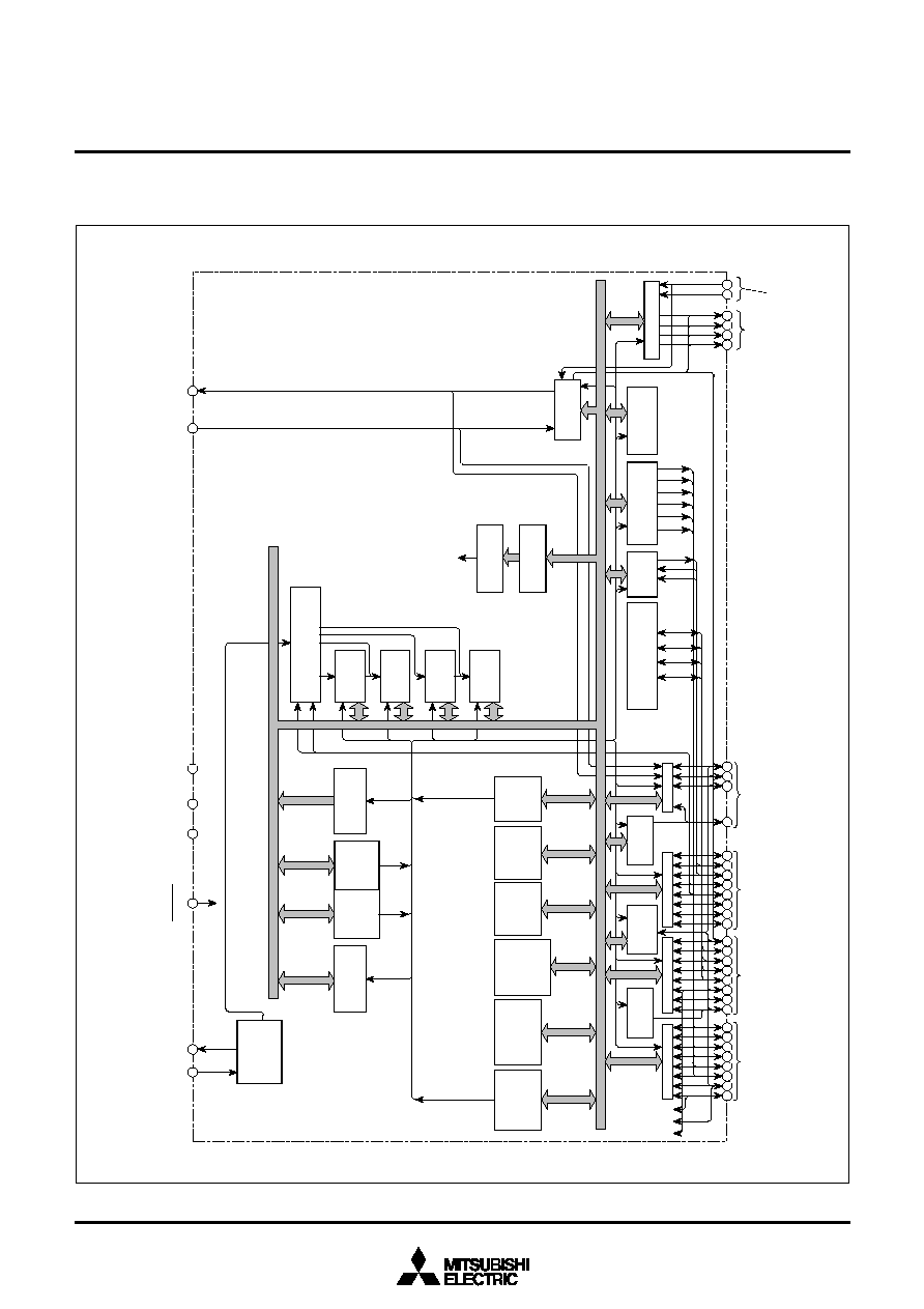
5. FUNCTIONAL BLOCK DIAGRAM
Fig. 5.1 Functional Block Diagram of M37225
O
U
T
1
C
l
o
c
k
i
n
p
u
t
C
l
o
c
k
o
u
t
p
u
t
X
I
N
X
O
U
T
R
e
s
e
t
i
n
p
u
t
V
C
C
V
S
S
C
N
V
S
S
I
n
p
u
t
p
o
r
t
s
P
3
3
,
P
3
4
O
S
C
1
O
S
C
2
C
l
o
c
k
i
n
p
u
t
f
o
r
O
S
D
P
W
M
5
P
W
M
4
P
W
M
3
P
W
M
2
P
W
M
1
P
W
M
0
P
5
(
6
)
B
G
R
H
S
Y
N
C
V
S
Y
N
C
1
4
-
b
i
t
P
W
M
c
i
r
c
u
i
t
1
8
-
b
i
t
P
W
M
c
i
r
c
u
i
t
A
c
c
u
m
u
l
a
t
o
r
A
(
8
)
T
i
m
e
r
4
T
4
(
8
)
T
i
m
e
r
3
T
3
(
8
)
T
i
m
e
r
2
T
2
(
8
)
T
i
m
e
r
1
T
1
(
8
)
T
i
m
e
r
c
o
u
n
t
s
o
u
r
c
e
s
e
l
e
c
t
i
o
n
c
i
r
c
u
i
t
T
I
M
2
T
I
M
3
I
n
s
t
r
u
c
t
i
o
n
r
e
g
i
s
t
e
r
(
8
)
I
n
s
t
r
u
c
t
i
o
n
d
e
c
o
d
e
r
C
o
n
t
r
o
l
s
i
g
n
a
l
O
S
D
c
i
r
c
u
i
t
S
t
a
c
k
p
o
i
n
t
e
r
S
(
8
)
I
n
d
e
x
r
e
g
i
s
t
e
r
X
(
8
)
P
r
o
c
e
s
s
o
r
s
t
a
t
u
s
r
e
g
i
s
t
e
r
P
S
(
8
)
8
-
b
i
t
a
r
i
t
h
m
e
t
i
c
a
n
d
l
o
g
i
c
a
l
u
n
i
t
R
O
M
P
r
o
g
r
a
m
c
o
u
n
t
e
r
P
C
L
(
8
)
P
r
o
g
r
a
m
c
o
u
n
t
e
r
P
C
H
(
8
)
R
A
M
D
a
t
a
b
u
s
C
l
o
c
k
g
e
n
e
r
a
t
i
n
g
c
i
r
c
u
i
t
R
E
S
E
T
O
u
t
p
u
t
p
o
r
t
s
P
5
2
P
5
5
O
S
D
o
u
t
p
u
t
A
d
d
r
e
s
s
b
u
s
S
I
/
O
(
8
)
S
I
N
S
C
L
K
S
O
U
T
I
N
T
2
I
N
T
1
I
N
T
3
I
/
O
p
o
r
t
s
P
3
0
P
3
2
,
P
3
5
1
7
2
6
2
7
1
6
P
3
(
6
)
3
9
4
0
4
1
4
2
2
1
2
0
1
9
2
5
2
2
2
1
1
8
2
4
2
3
I
n
d
e
x
r
e
g
i
s
t
e
r
Y
(
8
)
M
u
l
t
i
-
m
a
s
t
e
r
I
2
C
-
B
U
S
i
n
t
e
r
f
a
c
e
R
O
M
c
o
r
r
e
c
t
i
o
n
f
u
n
c
t
i
o
n
S
y
n
c
s
i
g
n
a
l
i
n
p
u
t
I
n
p
u
t
p
o
r
t
s
P
5
0
,
P
5
1
S
D
A
2
S
D
A
1
S
C
L
2
S
C
L
1
A
-
D
c
o
n
v
e
r
t
e
r
1
0
9
8
7
6
5
4
3
I
/
O
p
o
r
t
P
0
2
8
2
9
3
0
3
1
3
2
3
3
3
4
3
5
P
1
(
8
)
I
/
O
p
o
r
t
P
1
1
5
1
4
1
3
1
2
1
1
3
6
3
7
3
8
P
2
(
8
)
I
/
O
p
o
r
t
P
2
P
0
(
8
)
1
4
-
b
i
t
P
W
M
c
i
r
c
u
i
t
2
O
U
T
2
C
l
o
c
k
o
u
t
p
u
t
f
o
r
O
S
D
5
SINGLE-CHIP 8-BIT CMOS MICROCOMPUTER for VOLTAGE SYNTHESIZER
with ON-SCREEN DISPLAY CONTROLLER
M37225M6XXXSP, M37225M8XXXSP
M37225ECSP
MITSUBISHI MICROCOMPUTERS
Rev. 1.0
Number of basic instructions
Instruction execution time
Clock frequency
Memory size
Input/Output
ports
Serial I/O
Multi-master I
2
C-BUS interface
A-D converter
PWM output circuit
Timers
ROM correction function
Subroutine nesting
Interrupt
Clock generating circuit
ROM
RAM
OSD ROM
OSD RAM
P0
0
P0
5
P0
6
, P0
7
P1
P2
P3
0
, P3
1
, P3
5
P3
2
P3
3
, P3
4
P5
0
, P5
1
P5
2
P5
5
I/O
I/O
I/O
I/O
I/O
I/O
Input
Input
Output
71
0.5
µ
s (the minimum instruction execution time, at 8 MHz oscillation fre-
quency)
8 MHz (maximum)
24K bytes
32K bytes
48K bytes
1024 bytes (ROM correction memory included)
2048 bytes (ROM correction memory included)
15K bytes
96 bytes
6-bit
!
1 (N-channel open-drain output structure, can be used as PWM
output pins)
2-bit
!
1 (N-channel open-drain output structure, can be used as INT input
pins, A-D input pin)
8-bit
!
1 (CMOS input/output structure, can be used as OSD output pin, INT
input pin, A-D input pins, DA output pin, multi-master I
2
C-BUS interface)
8-bit
!
1 (CMOS input/output structure, can be used as serial I/O pins,
timer external clock input pins)
3-bit
!
1 (CMOS output structure, or N-channel open-drain output struc-
ture, can be used as A-D input pins, DA output pin)
1-bit
!
1 (N-channel open-drain output structure, can be used as A-D input pin)
2-bit
!
1 (Can be used as OSD clock input/output pins)
2-bit
!
1 (N-channel open-drain output structure, can be used as horizonal
· vertical synchronous sibnal input pins)
4-bit
!
1 (CMOS output structure, can be used as OSD output pins)
8-bit
!
1
1 (2 systems)
8 channels (8-bit resolution)
14-bit
!
2, 8-bit
!
6
8-bit timer
!
4
3 vectors
128 levels (maximum)
<16 types>
INT external interrupt
!
3, Internal timer interrupt
!
6, Serial I/O interrupt
!
1, OSD interrupt
!
1, Multi-master I
2
C-BUS interface interrupt
!
1,
f(X
IN
)/4096 interrupt
!
1, SPRITE OSD interrupt
!
1, A-D conversion inter-
rupt
!
1, V
SYNC
interrupt
!
1, BRK instruction interrupt
!
1, reset
!
1
2 built-in circuits (externally connected to a ceramic resonator or a quartz-
crystal oscillator)
Parameter
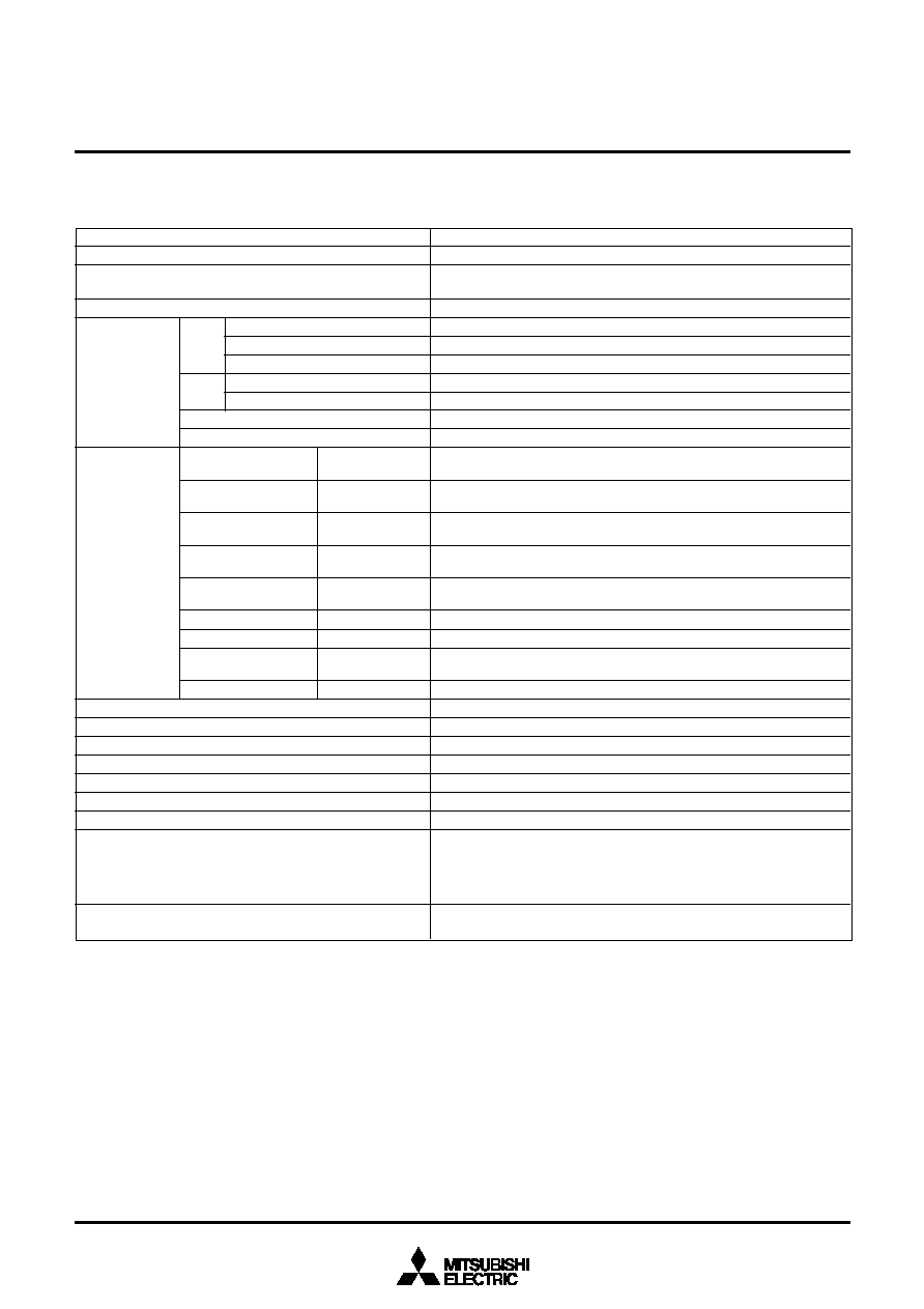
6. PERFORMANCE OVERVIEW
M37225M6-XXXSP
M37225M8-XXXSP
M37225ECSP
M37225M6-XXXSP, M37225M8-XXXSP
M37225ECSP
Table 6.1 Performance Overview
Functions
Document Outline
- Be Sure to Read
- Table of Contents
- SFR
- PDF Revision History