 | ÐлекÑÑоннÑй компоненÑ: M37272M6H | СкаÑаÑÑ:  PDF PDF  ZIP ZIP |
Äîêóìåíòàöèÿ è îïèñàíèÿ www.docs.chipfind.ru

1
SINGLE-CHIP 8-BIT CMOS MICROCOMPUTER with CLOSED CAPTION DECODER
and ON-SCREEN DISPLAY CONTROLLER
M37272M6H/M8H/MAH/MFHXXXSP/FP
M37272E8SP/FP, M37272EFSP/FP
MITSUBISHI MICROCOMPUTERS
Rev. 1.0
1. DESCRIPTION
The M37272M6H/M8H/MAH/MFH-XXXSP/FP are single-chip micro-
computers designed with CMOS silicon gate technology. They have
a OSD, data slicer, and I
2
C-BUS interface, so it is useful for a chan-
nel selection system for TV with a closed caption decoder.
The features of the M37272E8SP/FP and M37272EFSP/FP are simi-
lar to those of the M37272M6H-XXXSP/FP except that the chip has
a built-in PROM which can be written electrically. The difference be-
tween M37272M6H/M8H/MAH/MFH-XXXSP/FP are the ROM size
and RAM size. Accordingly, the following descriptions will be for the
M37272M6H-XXXSP/FP.
2. FEATURES
q
Number of basic instructions .................................................... 71
q
Memory size
ROM .............. 24K bytes
(M37272M6H-XXXSP/FP)
32K bytes
(M37272M8H-XXXSP/FP, M37272E8SP/FP)
40K bytes
(M37272MAH-XXXSP/FP)
60K bytes
(M37272MFH-XXXSP/FP, M37272EFSP/FP)
RAM ............... 1024 bytes
(M37272M6H-XXXSP/FP)
1152 bytes
(M37272M8H-XXXSP/FP, M37272E8SP/FP)
1472 bytes
(M37272MAH-XXXSP/FP, M37272MFH- .
XXXSP/FP, M37272EFSP/FP)
(*ROM correction memory included)
q
Minimum instruction execution time
......................................... 0.5
µ
s
(at 8 MHz oscillation frequency)
q
Power source voltage ................................................. 5 V ± 10 %
q
Subroutine nesting ............................................. 128 levels (Max.)
q
Interrupts ....................................................... 17 types, 16 vectors
q
8-bit timers .................................................................................. 6
q
Programmable I/O ports (Ports P0, P1, P2, P3
0
, P3
1
) ............. 26
q
Input ports (Ports P5
0
, P5
1
) ........................................................ 2
q
Output ports (Ports P5
2
P5
5
) ..................................................... 4
q
12 V withstand ports ................................................................... 6
q
LED drive ports ........................................................................... 4
q
Serial I/O ............................................................ 8-bit
1 channel
q
Multi-master I
2
C-BUS interface .............................. 1 (2 systems)
q
A-D comparator (6-bit resolution) ................................ 6 channels
q
PWM output circuit ......................................................... 8-bit
6
q
Power dissipation
In high-speed mode ......................................................... 165 mW
(at V
CC
= 5.5V, 8 MHz oscillation frequency, OSD on, and Data
slicer on)
In low-speed mode ......................................................... 0.33 mW
(at V
CC
= 5.5V, 32 kHz oscillation frequency)
q
ROM correction function ................................................ 2 vectors
q
Closed caption data slicer
q
OSD function
Display characters ................................... 32 characters
2 lines
(It is possible to display 3 lines or more by software)
Kinds of characters ........................................................ 254 kinds
Character display area ............................ CC mode: 16
26 dots
OSD mode: 16
20 dots
Kinds of character sizes ..................................... CC mode: 1 kind
OSD mode: 8 kinds
Kinds of character colors .................................. 8 colors (R, G, B)
Coloring unit ................... character, character background, raster
Display position
Horizontal: 128 levels
Vertical: 512 levels
Attribute ........................................................................................
CC mode: smooth italic, underline, flash, automatic solid space
OSD mode: border
Smoth roll-up
Window function
3. APPLICATION
TV with a closed caption decoder

2
SINGLE-CHIP 8-BIT CMOS MICROCOMPUTER with CLOSED CAPTION DECODER
and ON-SCREEN DISPLAY CONTROLLER
M37272M6H/M8H/MAH/MFHXXXSP/FP
M37272E8SP/FP, M37272EFSP/FP
MITSUBISHI MICROCOMPUTERS
Rev. 1.0
TABLE OF CONTENTS
1. DESCRIPTION .......................................................................... 1
2. FEATURES ................................................................................ 1
3. APPLICATION ............................................................................ 1
4. PIN CONFIGURATION .............................................................. 3
5. FUNCTIONAL BLOCK DIAGRAM ............................................. 4
6. PERFORMANCE OVERVIEW ................................................... 5
7. PIN DESCRIPTION ................................................................... 7
8. FUNCTIONAL DESCRIPTION ................................................. 11
8.1 CENTRAL PROCESSING UNIT (CPU) .................... 11
8.2 MEMORY .................................................................. 12
8.3 INTERRUPTS ........................................................... 18
8.4 TIMERS ..................................................................... 23
8.5 SERIAL I/O ................................................................ 26
8.6 MULTI-MASTER I2C-BUS INTERFACE ................... 29
8.7 PWM OUTPUT FUNCTION ...................................... 42
8.8 A-D COMPARATOR .................................................. 46
8.9 ROM CORRECTION FUNCTION ............................. 48
8.10 DATA SLICER ......................................................... 49
8.11 OSD FUNCTIONS ................................................... 60
8.11.1 Display Position ....................................... 65
8.11.2 Dot Size ................................................... 69
8.11.3 Clock for OSD .......................................... 70
8.11.4 Field Determination Display ..................... 71
8.11.5 Memory for OSD ...................................... 73
8.11.6 Character color ........................................ 77
8.11.7 Character background color .................... 77
8.11.8 OUT1, OUT2 signals ............................... 78
8.11.9 Attribute .................................................... 79
8.11.10 Multiline Display ..................................... 84
8.11.11 Automatic Solid Space Function ............ 85
8.11.12 Window Function ................................... 86
8.11.13 OSD Output Pin Control ........................ 88
8.11.14 Raster Coloring Function ....................... 89
8.12 SOFTWARE RUNAWAY DETECT FUNCTION ...... 91
8.13. RESET CIRCUIT .................................................... 92
8.14 CLOCK GENERATING CIRCUIT ............................ 93
8.15 DISPLAY OSCILLATION CIRCUIT ......................... 96
8.16 AUTO-CLEAR CIRCUIT .......................................... 96
8.17 ADDRESSING MODE ............................................. 96
8.18 MACHINE INSTRUCTIONS .................................... 96
9. PROGRAMMING NOTES ........................................................ 96
10. ABSOLUTE MAXIMUM RATINGS ......................................... 97
11. RECOMMENDED OPERATING CONDITIONS ..................... 97
12. ELECTRIC CHARACTERISTICS .......................................... 98
13. A-D CONVERTER CHARACTERISTICS ............................. 100
14. MULTI-MASTER I2C-BUS BUS LINE CHARACTERISTICS ......... 100
15. PROM PROGRAMMING METHOD ..................................... 101
16. DATA REQUIRED FOR MASK ORDERS ............................ 102
17. ONE TIME PROM VERSION M37272E8SP/FP, M37272EFSP/FP MARKING ...... 103
18. APPENDIX .......................................................................... 104
19. PACKAGE OUTLINE ........................................................... 129
3
SINGLE-CHIP 8-BIT CMOS MICROCOMPUTER with CLOSED CAPTION DECODER
and ON-SCREEN DISPLAY CONTROLLER
M37272M6H/M8H/MAH/MFHXXXSP/FP
M37272E8SP/FP, M37272EFSP/FP
MITSUBISHI MICROCOMPUTERS
Rev. 1.0
1
2
3
4
5
6
7
8
9
1
0
1
1
1
2
1
3
1
4
1
5
16
17
1
8
1
9
2
0
2
1
42
4
1
40
39
3
8
3
7
3
6
3
5
3
4
3
3
3
2
3
1
3
0
2
9
2
8
27
26
2
5
24
2
3
22
P0
6
/INT2/AD4
X
OUT
P5
0
/H
SYNC
P5
1
/V
SYNC
P
0
0
/
P
W
M
0
P0
1
/PWM1
P0
2
/PWM2
P
0
3
/
P
W
M
3
P
0
4
/
P
W
M
4
P
0
5
/
P
W
M
5
P
0
7
/
I
N
T
1
P
2
3
/
T
I
M
3
P
2
4
/
T
I
M
2
P
2
5
HLF
V
H
O
L
D
CV
IN
CNV
SS
X
IN
V
SS
P
5
2
/
R
P5
3
/G
P5
4
/B
P5
5
/OUT1
P2
0
/S
CLK
P
2
1
/
S
O
U
T
P
2
2
/
S
I
N
P
1
0
/
O
U
T
2
P
1
1
/
S
C
L
1
P
1
2
/
S
C
L
2
P
1
3
/
S
D
A
1
P
1
4
/
S
D
A
2
P
1
5
/
A
D
1
/
I
N
T
3
P
1
6
/
A
D
2
P
3
0
/
A
D
5
P
3
1
/
A
D
6
R
E
S
E
T
P
2
6
/
O
S
C
1
/
X
C
I
N
P
2
7
/
O
S
C
2
/
X
C
O
U
T
V
C
C
P
1
7
/
A
D
3
M37272M6H/M8H/MAH/MFH-XXXSP
M37272E8/EFSP
(AV
CC
) NC
( )...M37272E8/EFSP
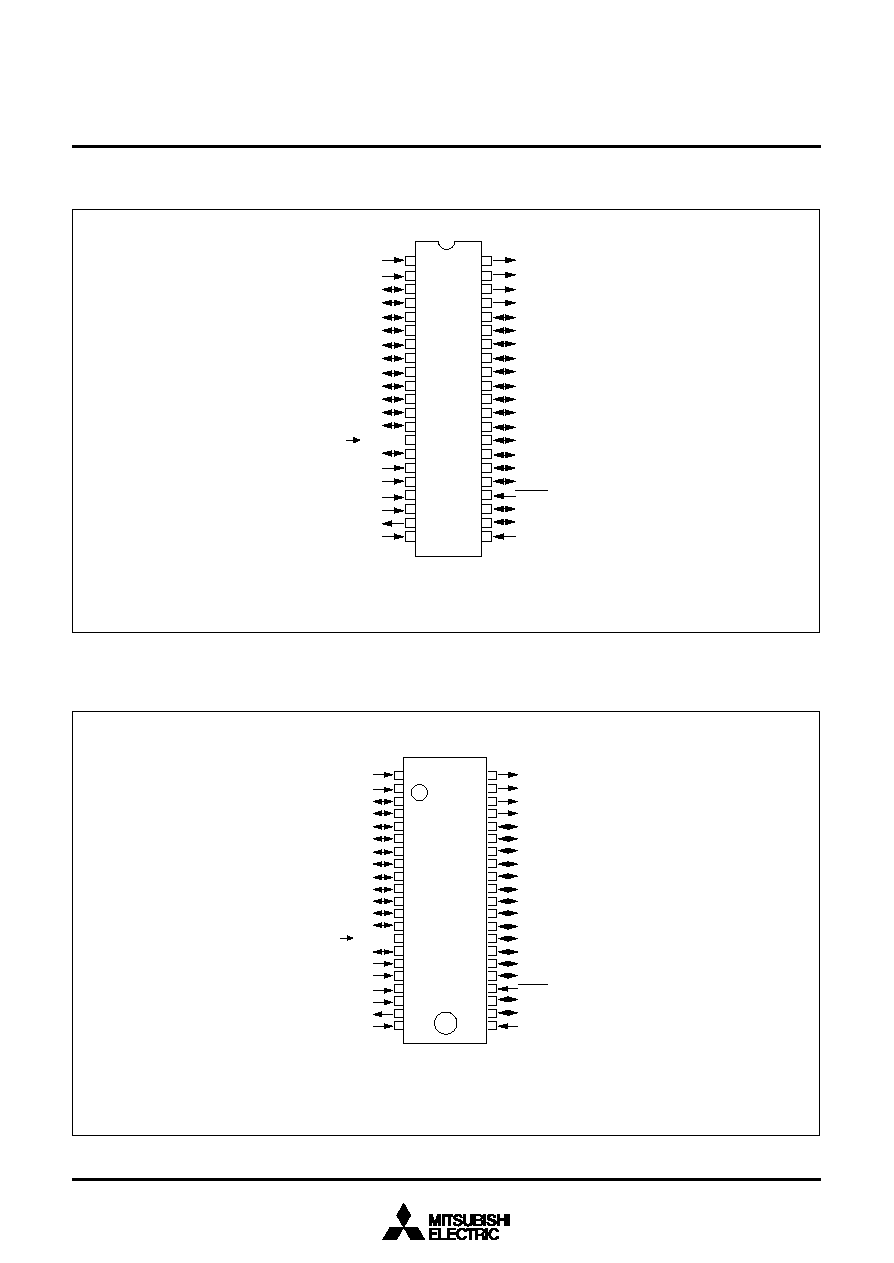
4. PIN CONFIGURATION
Outline 42P4B
Fig. 4.1 Pin Configuration (1) (Top View)
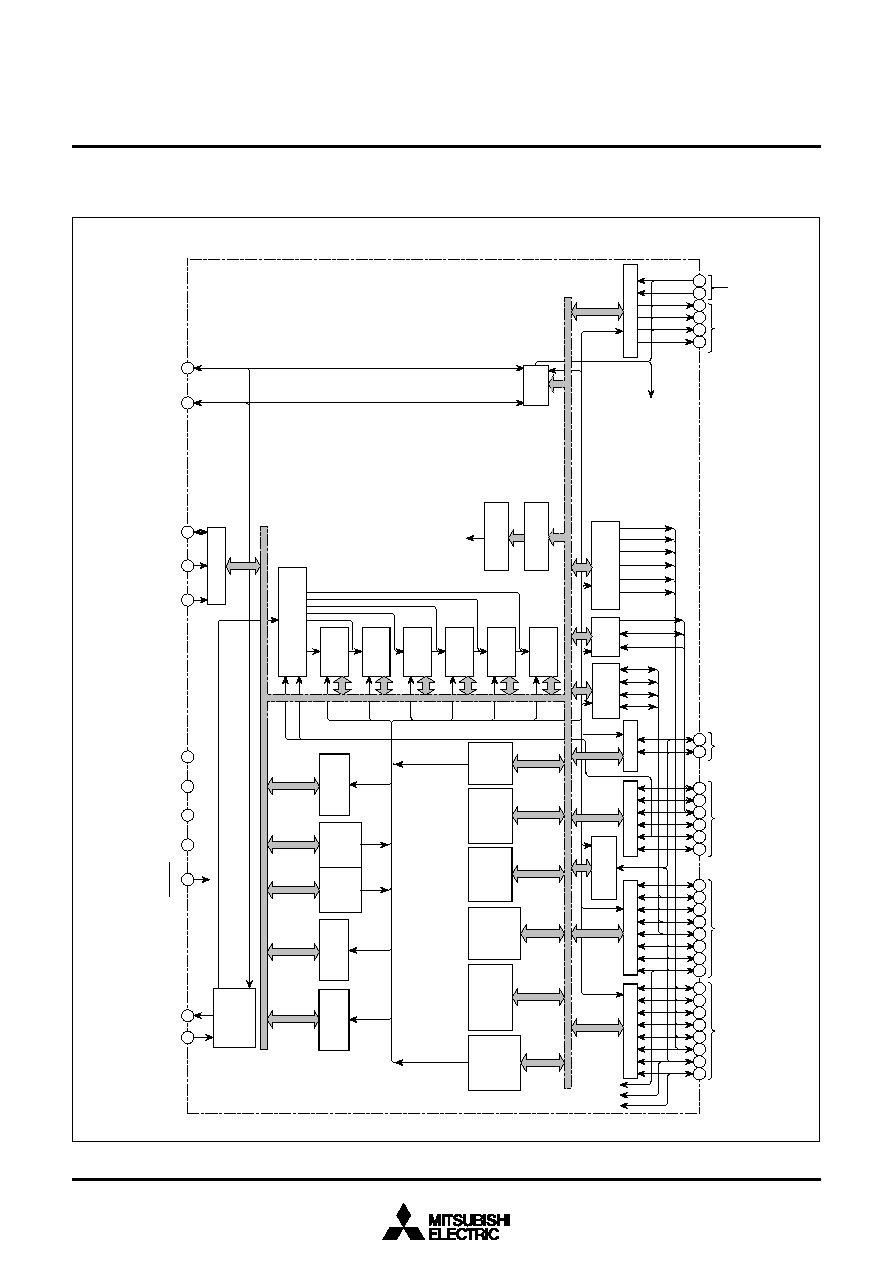
Outline 42P2R-A/E
Fig. 4.2 Pin Configuration (2) (Top View)
1
2
3
4
5
6
7
8
9
1
0
1
1
1
2
1
3
1
4
15
16
1
7
1
8
1
9
20
2
1
P0
6
/INT2/AD4
X
OUT
P5
0
/H
SYNC
P
5
1
/
V
S
Y
N
C
P
0
0
/
P
W
M
0
P
0
1
/
P
W
M
1
P
0
2
/
P
W
M
2
P
0
3
/
P
W
M
3
P
0
4
/
P
W
M
4
P
0
5
/
P
W
M
5
P
0
7
/
I
N
T
1
P
2
3
/
T
I
M3
P
2
4
/
T
I
M
2
P
2
5
HLF
V
HOLD
CV
IN
C
N
V
S
S
X
IN
V
S
S
42
41
40
39
38
37
36
35
34
33
32
31
30
29
28
27
26
25
24
23
22
P5
2
/R
P
5
3
/
G
P
5
4
/
B
P
5
5
/
O
U
T
1
P
2
0
/
S
C
L
K
P
2
1
/
S
O
U
T
P
2
2
/
S
I
N
P
1
0
/
O
U
T
2
P
1
1
/
S
C
L
1
P
1
2
/
S
C
L
2
P
1
3
/
S
D
A
1
P
1
4
/
S
D
A
2
P
1
5
/
A
D
1
/
I
N
T
3
P
1
6
/
A
D
2
P
3
0
/
A
D
5
P3
1
/AD6
RESET
P2
6
/OSC1/X
CIN
P2
7
/OSC2/X
COUT
V
C
C
P
1
7
/
A
D
3
M37272M6H/M8H/MAH/MFH-XXXFP
M37272E8/EFFP
(AV
CC
) NC
( )...M37272E8/EFFP
Note: Only 14th pin is NC pin of M37272M6H/
M8H/MAH/MFH-XXXSP. This pin is
AVcc pin of M37272E8/EFSP. But NC
pin of M37272M6H/M8H/MAH/MFH-
XXX SP is not connect in the IC. You
can apply to Vcc.
Note: Only 14th pin is NC pin of M37272M6H/
M8H/MAH/MFH-XXXFP. This pin is
AVcc pin of M37272E8/EFSP. But NC
pin of M37272M6H/M8H/MAH/MFH-
XXX SP is not connect in the IC. You
can apply to Vcc.
4
SINGLE-CHIP 8-BIT CMOS MICROCOMPUTER with CLOSED CAPTION DECODER
and ON-SCREEN DISPLAY CONTROLLER
M37272M6H/M8H/MAH/MFHXXXSP/FP
M37272E8SP/FP, M37272EFSP/FP
MITSUBISHI MICROCOMPUTERS
Rev. 1.0
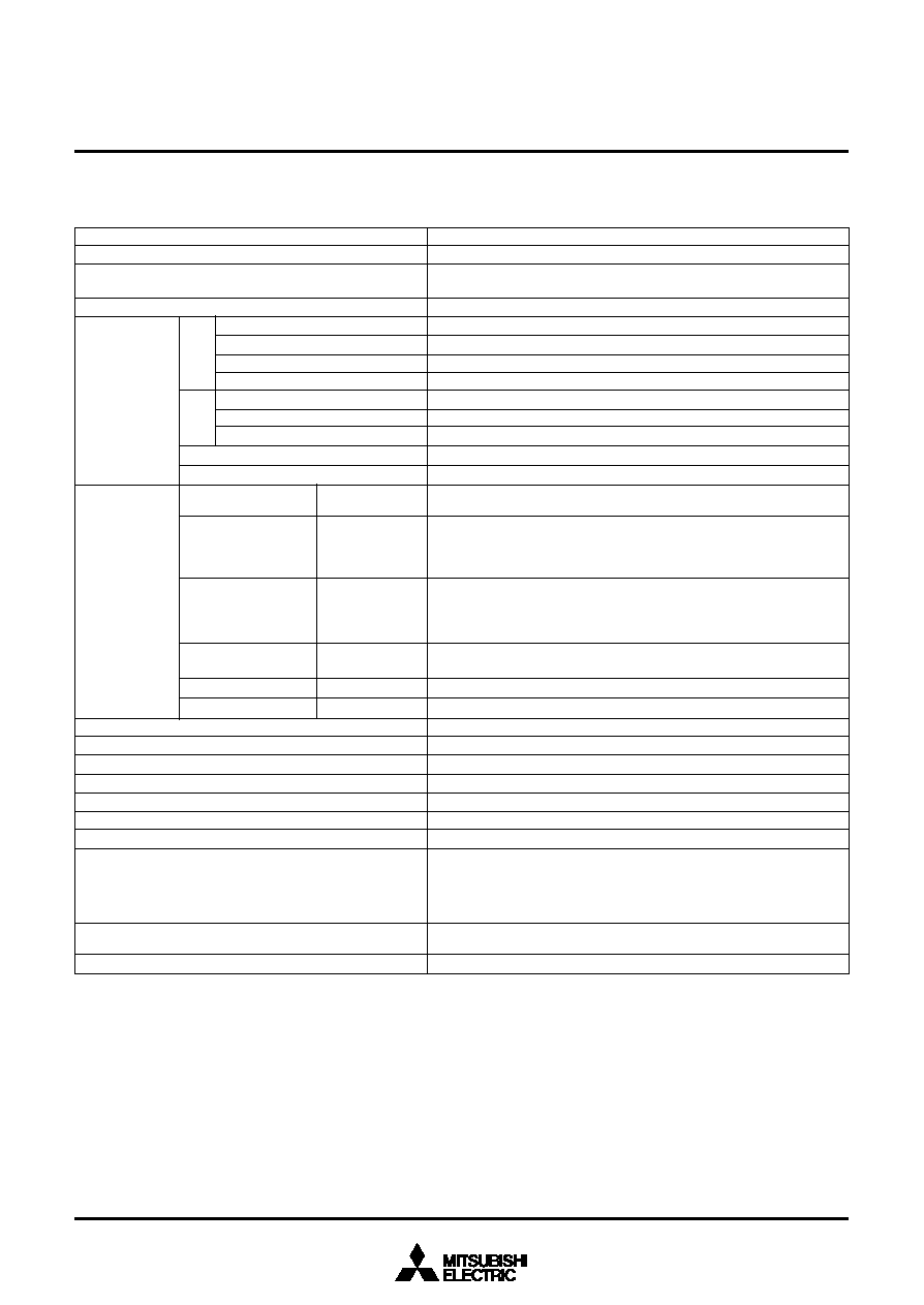
5. FUNCTIONAL BLOCK DIAGRAM
Fig. 5.1 Functional Block Diagram of M37272
X
I
N
X
O
U
T
OS
C1/X
CI
N
O
S
C
2
/
X
C
O
U
T
P
0
(
8
)
I
N
T
1
I
N
T
2
I
N
T
3
P
1
(
8
)
P
W
M
5
P
W
M
4
P
W
M
3
P
W
M
2
P
W
M
1
P
W
M
0
P
W
M
TI
M2
TI
M3
1
9
2
0
25
14
2
22
1
1
8
CV
IN
1
71
61
5
V
HO
L
D
HL
F
2
42
3
1
0
987
65
4
3
2
82
93
03
13
23
33
43
5
P
2
(
8
)
13
1
21
13
63
7
I
/
O
p
o
r
t
P
1I
/
O
p
o
r
t
P
2
P
3
(
2
)
27
2
6
3
8
S
D
A
2
S
D
A
1
S
C
L
2
S
C
L
1
S
I
/
O
S
I
N
S
C
L
K
S
O
U
T
P
5
(
6
)
3
94
04
14
22
O
u
t
p
u
t
p
o
r
t
s
P
5
2
--
P
5
5
O
u
t
p
u
t
f
o
r
d
i
s
p
l
a
y
1
H
S
Y
N
C
V
S
Y
N
C
R
G
B
O
U
T
1
O
U
T
2
P
1
0
I
/
O
p
o
r
t
s
P
3
0
,
P
3
1
A
D
1
--
6
D
a
t
a
s
l
i
c
e
r
Contr
o
l signal
X
I
N
X
O
U
T
Resetinput
V
CC
V
S
S
C
N
V
S
S
P
i
n
s
f
o
r
d
a
t
a
s
l
i
c
e
r
Clock out
put fo
r
OS
D
/
sub-
clock outp
u
t
I
/
O
p
o
r
t
s
P
2
6
,
P
2
7
C
l
o
ck input fo
r
OS
D/su
b-clock in
p
u
t
A-
D
c
o
mp
arat
or
8
-
b
i
t
a
r
i
t
h
m
e
t
i
c
a
n
d
l
o
g
i
c
a
l
u
n
i
t
A
c
c
u
m
u
l
a
t
o
r
A
(
8
)
T
i
m
e
r
6
T
6
(
8
)
T
i
m
e
r
5
T
5
(
8
)
T
i
m
e
r
4
T
4
(
8
)
T
i
mer 3
T3
(
8
)
T
i
m
e
r
2
T
2
(
8
)
T
i
mer 1
T1
(
8
)
T
i
m
e
r
c
o
u
n
t
s
o
u
r
c
e
s
e
l
e
c
t
i
o
n
c
i
r
c
u
i
t
I
n
s
t
r
u
c
t
i
o
n
r
e
g
i
s
t
e
r
(
8
)
I
n
s
t
r
u
c
t
i
o
n
d
e
c
o
d
e
r
O
S
D
c
i
r
c
u
i
t
P
r
o
c
e
s
s
o
r
s
t
a
t
u
s
r
e
g
i
s
t
e
r
P
S
(
8
)
S
t
a
c
k
p
o
i
n
t
e
r
S
(
8
)
I
n
d
e
x
r
e
g
i
s
t
e
r
Y
(
8
)
I
n
d
ex
re
g
i
s
t
e
r
X (
8
)
ROM
P
r
o
g
r
a
m
c
o
u
n
t
e
r
P
C
L
(
8
)
P
r
o
g
a
m
c
o
u
n
t
e
r
P
C
H
(
8
)
R
A
M
D
a
t
a
b
u
s
Clo
ck
gener
ati
n
g
cir
c
u
i
t
R
E
S
ET
V
IN
A
d
d
r
e
s
s
b
u
s
I/
O por
t P
0
R
O
M
c
o
rrec
t
ion
ci
r
c
u
i
t
Mu
l
t
i
-
ma
st
e
r
I2
C-
B
U
S
in
t
e
r
f
a
c
e
I
nput p
orts
P
5
0
, P5
1
S
y
n
c
hron
o
us signa
l
i
n
put
(AV
CC
*)
NC
*( )... M37272E8SP/FP, M37272EFSP/FP
Clock input Clock output
5
SINGLE-CHIP 8-BIT CMOS MICROCOMPUTER with CLOSED CAPTION DECODER
and ON-SCREEN DISPLAY CONTROLLER
M37272M6H/M8H/MAH/MFHXXXSP/FP
M37272E8SP/FP, M37272EFSP/FP
MITSUBISHI MICROCOMPUTERS
Rev. 1.0
Number of basic instructions
Instruction execution time
Clock frequency
Memory size
Input/Output
ports
Serial I/O
Multi-master I
2
C-BUS interface
A-D comparator
PWM output circuit
Timers
ROM correction function
Subroutine nesting
Interrupt
Clock generating circuit
Data slicer
ROM
RAM
OSD ROM
OSD RAM
P0
P1
0
P1
7
P2
0
P2
7
P3
0
, P3
1
P5
0
, P5
1
P5
2
P5
5
M37272M6H-XXXSP/FP
M37272M8H-XXXSP/FP,M37272E8SP/FP
M37272MAH-XXXSP/FP
M37272MFH-XXXSP/FP, M37272EFSP/FP
M37272M6H-XXXSP/FP
M37272M8H-XXXSP/FP,M37272E8SP/FP
M37272MAH-XXXSP/FP, M37272MFH-XXXSP/FP, M37272EFSP/FP
I/O
I/O
I/O
I/O
Input
Output
71
0.5
µ
s (the minimum instruction execution time, at 8 MHz oscillation fre-
quency)
8 MHz (maximum)
24K bytes
32K bytes
40K bytes
60K bytes
1024 bytes (ROM correction memory included)
1152 bytes (ROM correction memory included)
1472 bytes (ROM correction memory included)
10K bytes
128 bytes
8-bit
1 (N-channel open-drain output structure, can be used as PWM
output pins, INT input pins, A-D input pin)
8-bit
1 (CMOS input/output structure, however, N-channel open-drain
output structure, when P1
1
P1
4
are used as multi-master I
2
C-BUS inter-
face, can be used as OSD output pin, A-D input pins, INT input pin, multi-
master I
2
C-BUS interface)
8-bit
1 (P2 is CMOS input/output structure, however, N-channel open-
drain output structure when P2
0
and 2
1
are used as serial output, can be
used as serial input/output pins, timer external clock input pins, OSD clock
input/output pin, sub-clock input/output pins)
2-bit
1 (CMOS input/output or N-channel open-drain output structure,
can be used as A-D input pins)
2-bit
1 (can be used as OSD input pins)
4-bit
1 (CMOS output structure, can be used as OSD output pins)
8-bit
1
1 (2 systems)
6 channels (6-bit resolution)
8-bit
6
8-bit timer
6
2 vectors
128 levels (maximum)
<17 types>
INT external interrupt
3, Internal timer interrupt
6, Serial I/O interrupt
1, OSD interrupt
1, Multi-master I
2
C-BUS interface interrupt
1, Data
slicer interrupt
1, f(X
IN
)/4096 interrupt
1, V
SYNC
interrupt
1, BRK
instruction interrupt
1, reset
1
2 built-in circuits (externally connected to a ceramic resonator or a quartz-
crystal oscillator)
Built-in
Parameter
6. PERFORMANCE OVERVIEW
Table 6.1 Performance Overview
Functions
Document Outline