 | ÐлекÑÑоннÑй компоненÑ: M37280MK | СкаÑаÑÑ:  PDF PDF  ZIP ZIP |
Äîêóìåíòàöèÿ è îïèñàíèÿ www.docs.chipfind.ru

1. DESCRIPTION
The M37280MFXXXSP and M37280MK-XXXSP are single-chip
microcomputers designed with CMOS silicon gate technology. They
have a OSD function and a data slicer function, so it is useful for a
channel selection system for TV with a closed caption decoder.
The feautures of the M37280EKSP is similar to those of the
M37280MK-XXXSP except that the chip has a built-in PROM which
can be written electrically. The difference between M37280MK-XXXSP
and M37280MF-XXXSP are the ROM size and RAM size. Accord-
ingly, the following descriptions will be for the M37280MK-XXXSP.
2. FEATURES
q
Number of basic instructions .................................................... 71
q
Memory size
ROM ..................... 60K bytes (M37280MF-XXXSP)
80K bytes (M37280MK-XXXSP,
M37280EKSP)
RAM ..................... 1024 bytes (M37280MF-XXXSP)
1472 bytes (M37280MK-XXXSP,
M37280EKSP)
ROM correction memory ............................ 64 bytes
q
Minimum instruction execution time
......................................... 0.5
µ
s
(at 8 MHz oscillation frequency)
q
Power source voltage ................................................. 5 V ± 10 %
q
Subroutine nesting ............................................. 128 levels (Max.)
q
Interrupts ....................................................... 19 types, 16 vectors
q
8-bit timers .................................................................................. 6
q
Programmable I/O ports (Ports P0, P1, P2, P3
0
, P3
1
) ............. 26
q
Input ports (Ports P4
0
P4
6
, P6
3
, P6
4
, P7
0
P7
2
) ...................... 12
q
Output ports (Ports P3
2
, P4
7,
P5
,
P6
0
P6
2,
P6
5
P6
7
) .............. 16
q
12 V withstand ports ................................................................... 8
q
LED drive ports ........................................................................... 2
q
Serial I/O ............................................................ 8-bit
!
1 channel
q
Multi-master I
2
C-BUS interface .............................. 1 (2 systems)
q
A-D converter (8-bit resolution) .................................... 8 channels
q
PWM output circuit ......................................................... 8-bit
!
8
q
Power dissipation
In high-speed mode ......................................................... 165 mW
(at V
CC
= 5.5V, 8 MHz oscillation frequency, CRT on, and Data
slicer on)
In low-speed mode ......................................................... 0.33 mW
(at V
CC
= 5.5V, 32 kHz oscillation frequency)
q
ROM correction function
SINGLE-CHIP 8-BIT CMOS MICROCOMPUTER with CLOSED CAPTION DECODER
and ON-SCREEN DISPLAY CONTROLLER
M37280MFXXXSP, M37280MKXXXSP
M37280EKSP
PRELIMINAR
Y
Notice:
This is not a final specification.
Some paramentic limits are subject to change.
MITSUBISHI MICROCOMPUTERS
Rev. 1.0
q
Closed caption data slicer
q
OSD function
Display characters .... 32 characters
!
16 lines + RAM font (1 character)
(CC/OSD mode)(CDOSD mode)(RAM font)
Kinds of characters ......... 510 kinds
+ 62 kinds
+ 1 kind
(Coloring unit)
(a character) (a dot)
(a dot)
Triple layer function .......................................................................
2 layers selected from CC/CDOSD/OSD mode + RAM font layer
Character display area .............. CC/CDOSD mode: 16
!
26 dots
OSD mode/RAM font: 16
!
20 dots
Kinds of character sizes .................... CC mode/RAM font: 4 kinds
OSD/CDOSD mode: 14 kinds
Kinds of character colors ..............................................................
64 colors (4 adjustment levels for each R, G, B)
Coloring unit ............ dot, character, character background, raster
Blanking output OUT1, OUT2
Display position
Horizontal: 256 levels
Vertical :1024 levels
(RAM font can be set independently)
Attribute ........................................................................................
CC mode: smooth italic, underline, flash, automatic solid space
OSD mode: border, shadow
Window/Blank function
3. APPLICATION
TV with a closed caption decoder
4. PIN CONFIGURATION
Refer to page 3.
5. BLOCK DIAGRAM
Refer to page 4.
6. PERFORMANCE OVERVIEW
Refer to pages 5 and 6.
7. PIN DESCRIPTION
Refer to pages 7 to 11.

2
SINGLE-CHIP 8-BIT CMOS MICROCOMPUTER with CLOSED CAPTION DECODER
and ON-SCREEN DISPLAY CONTROLLER
M37280MFXXXSP, M37280MKXXXSP
M37280EKSP
MITSUBISHI MICROCOMPUTERS
PRELIMINAR
Y
Notice:
This is not a final specification.
Some paramentic limits are subject to change.
Rev. 1.0
TABLE OF CONTENTS
8. PIN CONFIGURATION ................................................................................................................................................................................... 3
9. FUNCTIONAL BLOCK DIAGRAM .................................................................................................................................................................. 4
10. PERFORMANCE OVERVIEW ...................................................................................................................................................................... 5
11. PIN DESCRIPTION ....................................................................................................................................................................................... 7
12. FUNCTIONAL DESCRIPTION .................................................................................................................................................................... 12
12.1 CENTRAL PROCESSING UNIT (CPU) ........................................................................................................................................... 12
12.2 MEMORY ......................................................................................................................................................................................... 13
12.3 INTERRUPTS .................................................................................................................................................................................. 21
12.4 TIMERS ............................................................................................................................................................................................ 26
12.5 SERIAL I/O ....................................................................................................................................................................................... 30
12.6 MULTI-MASTER I
2
C-BUS INTERFACE .......................................................................................................................................... 33
12.7 PWM OUTPUT CIRCUIT ................................................................................................................................................................. 46
12.8 A-D CONVERTER ............................................................................................................................................................................ 50
12.9 ROM CORRECTION FUNCTION .................................................................................................................................................... 54
12.10 DATA SLICER ................................................................................................................................................................................ 55
12.11 OSD FUNCTIONS .......................................................................................................................................................................... 66
13. SOFTWARE RUNAWAY DETECT FUNCTION ......................................................................................................................................... 117
14. RESET CIRCUIT ........................................................................................................................................................................................ 118
15. CLOCK GENERATING CIRCUIT............................................................................................................................................................... 119
15.1 OSCILLATION CONTROL .............................................................................................................................................................. 119
16. DISPLAY OSCILLATION CIRCUIT ........................................................................................................................................................... 122
17. AUTO-CLEAR CIRCUIT ............................................................................................................................................................................ 122
18. ADDRESSING MODE ............................................................................................................................................................................... 122
19. MACHINE INSTRUCTIONS ..................................................................................................................................................................... 122
20. PROGRAMMING NOTES ......................................................................................................................................................................... 122
21. ABSOLUTE MAXIMUM RATINGS ............................................................................................................................................................ 123
22. RECOMMENDED OPERATING CONDITIONS ........................................................................................................................................ 123
23. ELECTRIC CHARACTERISTICS ............................................................................................................................................................. 124
24. ANALOG R, G, B OUTPUT CHARACTERISTICS .................................................................................................................................... 126
25. A-D CONVERETER CHARACTERISTICS ............................................................................................................................................... 126
26. MULTI-MASTER I
2
C-BUS BUS LINE CHARACTERISTICS .................................................................................................................... 127
27. DATA REQUIRED FOR MASK ORDERS ................................................................................................................................................. 128
28. PROM PROGRAMMING METHOD .......................................................................................................................................................... 128
29. MASK CONFIRMATION FORM ................................................................................................................................................................ 129
30. MARK SPECIFICATION FORM ................................................................................................................................................................ 135
31. APPENDIX ................................................................................................................................................................................................ 136
32. PACKAGE OUTLINE ................................................................................................................................................................................ 176
3
SINGLE-CHIP 8-BIT CMOS MICROCOMPUTER with CLOSED CAPTION DECODER
and ON-SCREEN DISPLAY CONTROLLER
M37280MFXXXSP, M37280MKXXXSP
M37280EKSP
MITSUBISHI MICROCOMPUTERS
PRELIMINAR
Y
Notice:
This is not a final specification.
Some paramentic limits are subject to change.
Rev. 1.0
1
2
3
4
5
6
7
8
9
10
11
12
13
14
15
16
17
18
19
20
21
64
63
62
61
60
59
58
57
56
55
54
53
52
51
50
49
48
47
46
45
44
P5
0
/PWM7
HLF/AD6
H
SYNC
V
SYNC
P4
0
AD4
P4
1
/INT2
P4
2
/TIM2
P4
3
/TIM3
P2
4
/AD3
P2
5
/AD2
P0
1
/PWM5
P4
7
P0
2
/PWM6
P5
1
P1
7
/S
IN
/R0
P3
2
P4
4
/INT1
P5
6
P4
6
/S
CLK
AV
CC
P7
2
/(S
IN
)
P5
2
/R/R1
P5
3
/G/G1
P5
4
/B/B1
P5
5
/OUT1
P0
4
/PWM0
P0
5
/PWM1
P6
0
P1
0
/OUT2
P1
1
/SCL1
P1
2
/SCL2
P1
3
/SDA1
P1
4
/SDA2
P1
5
/G0
P1
6
/INT3/B0
P3
0
/AD7
P3
1
/AD8
RESET
P6
4
/OSC2/X
COUT
P6
3
/OSC1/X
CIN
V
CC
P0
3
/PWM7
P2
6
/AD1
P2
7
/AD5
P0
0
/PWM4
P4
5
/S
OUT
P5
7
P0
6
/PWM2
P6
1
P2
1
P2
2
P2
3
22
23
24
25
26
43
42
41
40
39
M37280MF-XXXSP, M37280MK-XXXSP,
M37280EKSP
P7
0
/CV
IN
P7
1
/V
HOLD
CNV
SS
X
OUT
X
IN
V
SS
27
28
29
30
31
32
38
37
36
35
34
33
P0
7
/PWM3
P6
2
P2
0
P6
5
P6
6
P6
7
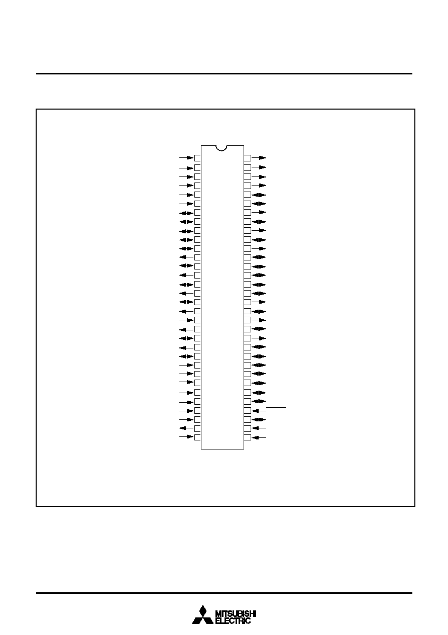
8. PIN CONFIGURATION
Outline 64P4B
Fig. 8.1 Pin Configuration (Top View)
4
SINGLE-CHIP 8-BIT CMOS MICROCOMPUTER with CLOSED CAPTION DECODER
and ON-SCREEN DISPLAY CONTROLLER
M37280MFXXXSP, M37280MKXXXSP
M37280EKSP
MITSUBISHI MICROCOMPUTERS
PRELIMINAR
Y
Notice:
This is not a final specification.
Some paramentic limits are subject to change.
Rev. 1.0
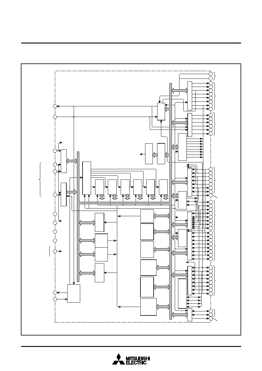
9. FUNCTIONAL BLOCK DIAGRAM
Fig. 9.1 Functional Block Diagram of M37280
Clock input
Clock output
X
IN
X
OUT
Reset input
AV
CC
V
CC
V
SS
CNV
SS
Pins for data
slicer
Clock output for
OSD/
sub-clock output
Input ports P6
3
, P6
4
OSC1
OSC2
Clock input
for
OSD/sub-clock input
P1 (8)
Multi-master
I2
C-BUS interface
P3 (3)
SDA1
SCL2
SCL1
SDA2
P2 (8)
P0 (8)
P4 (8)
S
IN
S
CLK
S
OUT
SI/O (8)
P6 (8)
INT1
INT2
PWM6
PWM5
PWM4
PWM3
PWM2
PWM1
PWM0
P5 (8)
OUT1
B
G
R
H
SYNC
V
SYNC
A-D
converter
8-bit
PWM circuit
8-bit
arithmetic
and
logical unit
Accumulator
A (8)
Timer 6
T6 (8)
Timer 5
T5 (8)
Timer 4
T4 (8)
Timer 3
T3 (8)
Timer 2
T2 (8)
Timer 1
T1 (8)
Timer count
source
selection circuit
TIM2
TIM3
Data slicer
Instruction
register (8)
Instruction
decoder
Control signal
OSD
circuit
Processor
status
register
PS (8)
Stack
pointer
S (8)
Index
register
Y (8)
Index
register
X (8)
ROM
Program
counter
PC
L
(8)
Progam
counter
PC
H
(8)
RAM
Data bus
Clock
generating
circuit
30
31
36
RESET
24
33
32
29
CV
IN
28
27
25
26
V
HOLD
RVCO
HLF
34
35
Address bus
36
17
40
41
42
43
45
47
49
10
9
8
7
50
51
52
53
55
57
59
60
39
15
13
11
23
21
19
6
5
4
3
61
62
63
64
2
1
I/O ports
P3
0
, P3
1
I/O port
P1
I/O port
P2
I/O port
P0
Input ports P4
0
P4
6
Output port P5
Sync
signal input
Output port P4
7
20
22
16
12
56
58
44
Output ports
P6
0
P6
2
, P6
5
P4
7
14
18
Output port
P3
2
INT3
PWM7
37
48
54
46
Input ports P7
0
P7
2
A-D converter
SI/O
P7 (3)
5
SINGLE-CHIP 8-BIT CMOS MICROCOMPUTER with CLOSED CAPTION DECODER
and ON-SCREEN DISPLAY CONTROLLER
M37280MFXXXSP, M37280MKXXXSP
M37280EKSP
MITSUBISHI MICROCOMPUTERS
PRELIMINAR
Y
Notice:
This is not a final specification.
Some paramentic limits are subject to change.
Rev. 1.0
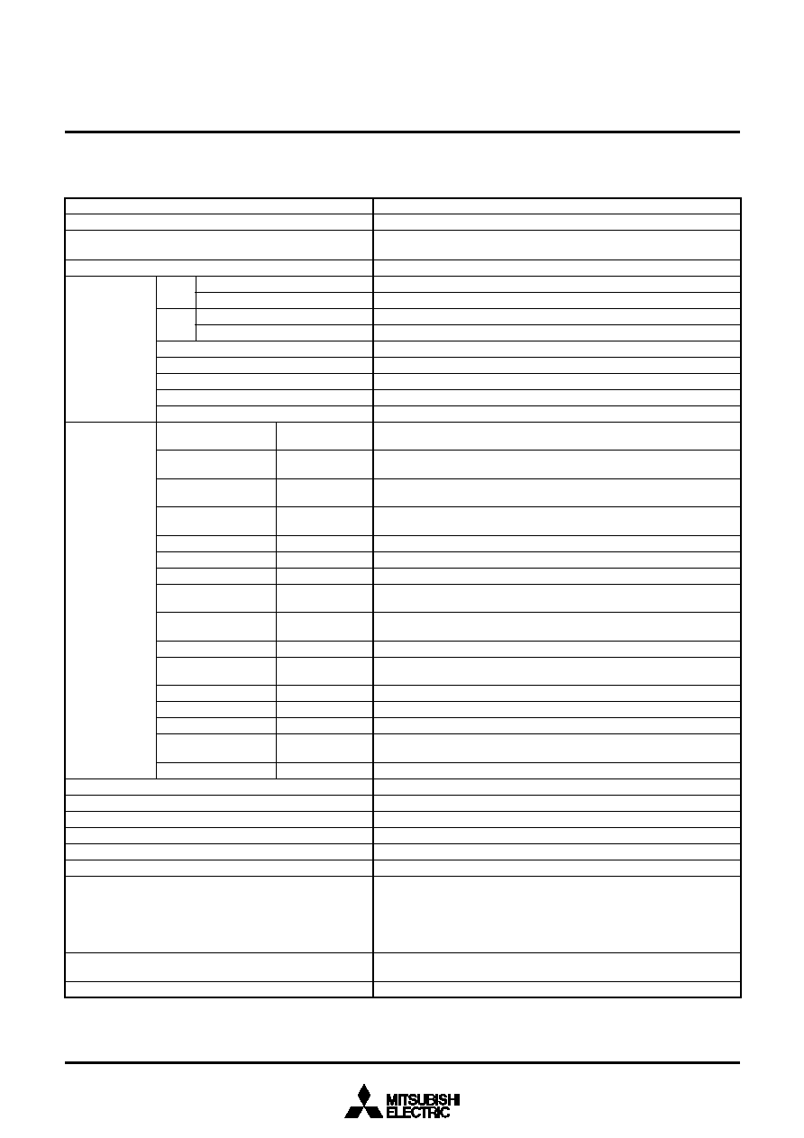
Number of basic instructions
Instruction execution time
Clock frequency
Memory size
Input/Output
ports
Serial I/O
Multi-master I
2
C-BUS interface
A-D converter
PWM output circuit
Timers
Subroutine nesting
Interrupt
Clock generating circuit
Data slicer
ROM
RAM
ROM correction memory
OSD ROM (character font)
OSD ROM (color dot font)
OSD RAM (SPRITE)
OSD RAM (character)
P0
0
P0
2
, P0
4
P0
7
P0
3
P1
0
, P1
5
P1
7
P1
1
P1
4
P2
P3
0
, P3
1
P3
2
P4
0
P4
4
P4
5
, P4
6
P4
7
P5
0
, P5
1
, P5
6
, P5
7
P5
2
P5
5
P6
0
P6
2
, P6
5
P6
7
P6
3
P6
4
P7
0
P7
2
I/O
I/O
I/O
I/O
I/O
I/O
Output
Input
Input
Output
Output
Output
Output
Input
Input
Input
71
0.5
µ
s (the minimum instruction execution time, at 8 MHz oscillation fre-
quency)
8 MHz (maximum)
60K bytes
80K bytes
1024 bytes
1472 bytes
64 bytes
20400 bytes
9672 bytes
120 bytes
1536 bytes
7-bit
!
1 (N-channel open-drain output structure, can be used as 8-bit PWM
output pins)
1-bit
!
1 (CMOS input/output structure, can be used as 14-bit PWM output
pin)
4-bit
!
1 (CMOS input/output structure, can be used as OSD output pin,
INT input pin, serial input pin)
4-bit
!
1 (N-channel open-drain output structure, can be used as multi-
master I
2
C-BUS interface)
8-bit
!
1 (CMOS input/output structure, can be used as A-D input pins)
2-bit
!
1 (CMOS input/output structure, can be used as A-D input pins)
1-bit
!
1 (N-channel open-drain output structure)
5-bit
!
1 (can be used as A-D input pins, INT input pins, external clock input
pins)
2-bit
!
1 (N-channel open-drain output structure when serial I/O is used,
can be used as serial I/O pins)
1-bit
!
1 (N-channel open-drain output structure)
4-bit
!
1 (N-channel open-drain output structure, can be used as PWM
output pin)
4-bit
!
1 (CMOS output structure, can be used as OSD output pins)
6-bit
!
1 (N-channel open-drain output structure)
1-bit
!
1 (can be used as sub-clock input pin, OSD clock input pin)
1-bit
!
1 (CMOS output structure when LC is oscillating, can be used as
sub-clock output pin, OSD clock output pin)
3-bit
!
1 (can be used as data slicer input/output, serial input pin)
8-bit
!
1
1 (2 systems)
8 channels (8-bit resolution)
8-bit
!
8
8-bit timer
!
6
128 levels (maximum)
<19 types>
External interrupt
!
3, Internal timer interrupt
!
6, Serial I/O interrupt
!
1,
OSD interrupt
!
1, Multi-master I
2
C-BUS interface interrupt
!
1,
Data slicer interrupt
!
1, f(X
IN
)/4096 interrupt
!
1, SPRITE OSD interrupt
!
1, V
SYNC
interrupt
!
1, A-D conversion interrupt
!
1, BRK instruction
interrupt
!
1
2 built-in circuits (externally connected to a ceramic resonator or a quartz-
crystal oscillator)
Built in
Parameter
10. PERFORMANCE OVERVIEW
M37280MF-XXXSP
M37280MK-XXXSP, M37280EKSP
M37280MF-XXXSP
M37280MK-XXXSP, M37280EKSP
Table 10.1 Performance Overview
Functions
Document Outline
- þÿ
- þÿ
- þÿ
- þÿ
- þÿ
- þÿ
- þÿ
- þÿ
- þÿ
- þÿ
- þÿ
- þÿ
- þÿ
- þÿ
- þÿ
- þÿ
- þÿ
- þÿ
- þÿ
- þÿ
- þÿ
- þÿ
- þÿ
- þÿ
- þÿ
- þÿ
- þÿ
- þÿ
- þÿ
- þÿ
- þÿ
- þÿ
- þÿ
- þÿ
- þÿ
- þÿ
- þÿ
- þÿ
- þÿ
- þÿ
- þÿ