 | –≠–ª–µ–∫—Ç—Ä–æ–Ω–Ω—ã–π –∫–æ–º–ø–æ–Ω–µ–Ω—Ç: M38027E4 | –°–∫–∞—á–∞—Ç—å:  PDF PDF  ZIP ZIP |
P4
1
/INT
0
25
26
27
28
29
30
31
32
33
34
35
36
37
38
39
40
1
2
3
4
5
6
7
8
9
10
11
12
13
14
15
16
17
18
19
20
21
22
23
24
48
49
50
51
52
53
54
55
56
57
58
59
60
61
62
63
64
P0
0
/AD
0
P0
3
/AD
3
P0
4
/AD
4
P0
5
/AD
5
P0
6
/AD
6
P0
7
/AD
7
P1
1
/AD
9
P1
2
/AD
10
P1
3
/AD
11
P1
4
/AD
12
P1
5
/AD
13
P1
6
/AD
14
P1
7
/AD
15
P6
2
/AN
2
P6
1
/AN
1
P6
0
/AN
0
P5
7
/INT
3
M38022M4-XXXFP
P5
6
/PWM
P5
5
/CNTR
1
P5
4
/CNTR
0
P5
2
/S
CLK2
P5
1
/S
OUT2
P5
0
/S
IN2
P4
7
/S
RDY1
P4
5
/T
X
D
P4
4
/R
X
D
P4
3
/INT
2
P6
3
/AN
3
P6
4
/AN
4
P6
5
/AN
5
AV
SS
V
REF
V
CC
P3
0
/DA
1
P3
1
/DA
2
P3
2
/ONW
P3
3
/RESET
OUT
P3
4
/
P3
5
/SYNC
P3
6
/WR
P3
7
/RD
P4
2
/INT
1
CNV
SS
X
IN
X
OUT
V
SS
P2
7
/DB
7
P2
6
/DB
6
P2
5
/DB
5
P2
4
/DB
4
P2
3
/DB
3
P2
2
/DB
2
P2
1
/DB
1
P2
0
/DB
0
RESET
P5
3
/S
RDY2
P4
6
/S
CLK1
P1
0
/AD
8
P0
1
/AD
1
P0
2
/AD
2
P4
0
/INT
4
P6
7
/AN
7
P6
6
/AN
6
41
42
43
44
45
46
47
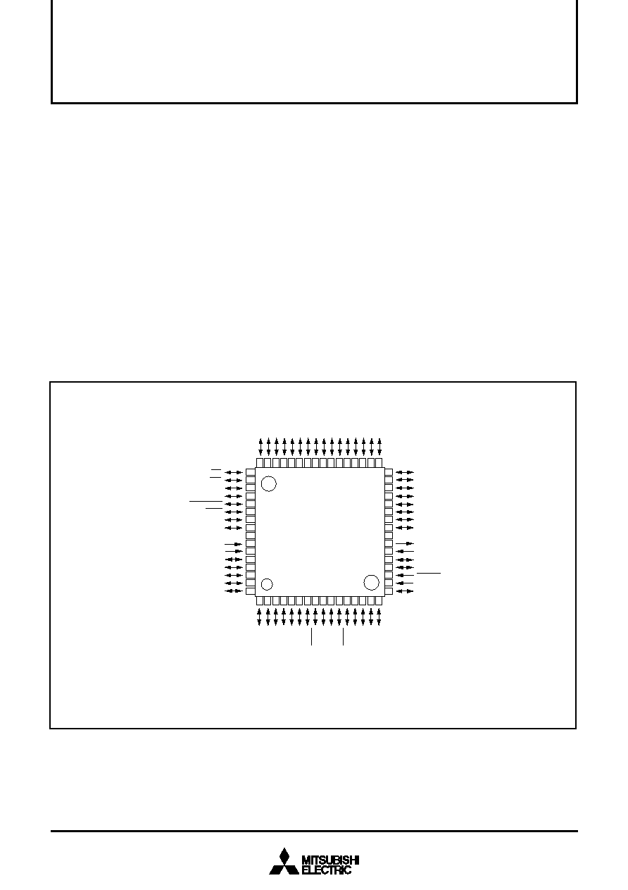
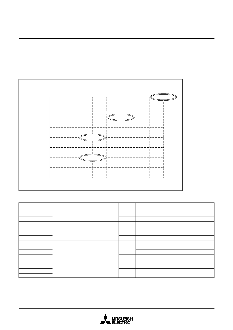
PIN CONFIGURATION (TOP VIEW)
Package type : 64P6N-A
64-pin plastic-molded QFP
DESCRIPTION
The 3802 group is the 8-bit microcomputer based on the 740 fam-
ily core technology.
The 3802 group is designed for controlling systems that require
analog signal processing and include two serial I/O functions, A-D
converters, and D-A converters.
The various microcomputers in the 3802 group include variations
of internal memory size and packaging. For details, refer to the
section on part numbering.
For details on availability of microcomputers in the 3802 group, re-
fer to the section on group expansion.
FEATURES
∑
Basic machine-language instructions ....................................... 71
∑
The minimum instruction execution time ............................ 0.5
µ
s
(at 8 MHz oscillation frequency)
∑
Memory size
ROM .................................................................. 8 K to 32 K bytes
RAM ................................................................. 384 to 1024 bytes
∑
Programmable input/output ports ............................................. 56
∑
Interrupts .................................................. 16 sources, 16 vectors
∑
Timers ............................................................................. 8 bit
!
4
∑
Serial I/O1 .................... 8-bit
!
1 (UART or Clock-synchronized)
∑
Serial I/O2 .................................... 8-bit
!
1 (Clock-synchronized)
∑
PWM ................................................................................ 8-bit
!
1
∑
A-D converter .................................................. 8-bit
!
8 channels
∑
D-A converter .................................................. 8-bit
!
2 channels
∑
Clock generating circuit ....................... Internal feedback resistor
(connect to external ceramic resonator or quartz-crystal oscillator)
∑
Power source voltage .................................................. 3.0 to 5.5 V
(Extended operating temperature version : 4.0 to 5.5 V)
∑
Power dissipation ............................................................... 32 mW
∑
Memory expansion possible
∑
Operating temperature range .................................... ≠20 to 85
∞
C
(Extended operating temperature version : ≠40 to 85
∞
C)
APPLICATIONS
Office automation, VCRs, tuners, musical instruments, cameras,
air conditioners, etc.
MITSUBISHI MICROCOMPUTERS
3802 Group
SINGLE-CHIP 8-BIT CMOS MICROCOMPUTER
MITSUBISHI MICROCOMPUTERS
3802 Group
SINGLE-CHIP 8-BIT CMOS MICROCOMPUTER
2
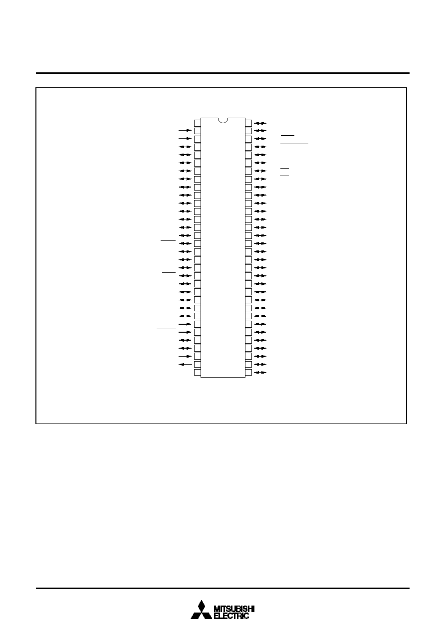
PIN CONFIGURATION (TOP VIEW)
Package type : 64P4B
64-pin shrink plastic-molded DIP
1
2
3
4
5
6
7
8
9
10
11
12
13
14
15
16
17
18
19
20
21
22
23
24
25
26
27
28
29
30
31
32
64
63
62
61
60
59
58
57
56
55
54
53
52
51
50
49
48
47
46
45
44
43
42
41
40
39
38
37
36
35
34
33
P6
4
/AN
4
P6
6
/AN
6
P6
7
/AN
7
AV
SS
V
REF
V
CC
P6
3
/AN
3
P6
5
/AN
5
P6
2
/AN
2
P6
1
/AN
1
P6
0
/AN
0
P5
7
/INT
3
P5
6
/PWM
P5
5
/CNTR
1
P5
4
/CNTR
0
P5
3
/S
RDY2
P5
2
/S
CLK2
P5
1
/S
OUT2
P5
0
/S
IN2
P4
7
/S
RDY1
P4
6
/S
CLK1
P4
3
/INT
2
P4
4
/R
X
D
P4
5
/T
X
D
CNV
SS
P4
1
/INT
0
P4
0
/INT
4
X
IN
X
OUT
V
SS
P4
2
/INT
1
RESET
P2
4
/DB
4
P2
3
/DB
3
P2
2
/DB
2
P2
0
/DB
0
P2
1
/DB
1
P2
5
/DB
5
P2
7
/DB
7
P2
6
/DB
6
P3
3
/RESET
OUT
P3
4
/
P3
5
/SYNC
P3
7
/RD
P3
6
/WR
P3
2
/ONW
P3
0
/DA
1
P3
1
/DA
2
P0
0
/AD
0
P0
1
/AD
1
P0
2
/AD
2
P0
3
/AD
3
P0
4
/AD
4
P0
5
/AD
5
P0
6
/AD
6
P0
7
/AD
7
P1
0
/AD
8
P1
1
/AD
9
P1
2
/AD
10
P1
3
/AD
11
P1
4
/AD
12
P1
7
/AD
15
P1
6
/AD
14
P1
5
/AD
13
M38022M4-XXXSP
MITSUBISHI MICROCOMPUTERS
3802 Group
SINGLE-CHIP 8-BIT CMOS MICROCOMPUTER
3
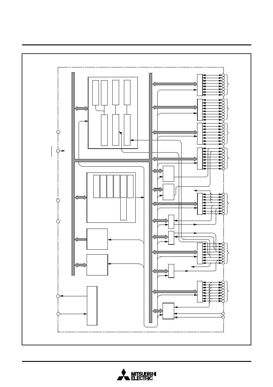
FUNCTIONAL BLOCK DIA
GRAM (P
ac
ka
g
e
:
64P4B)
CNTR
1
CNTR
0
V
REF
AV
SS
RAM
ROM
CPU
A
X
Y
S
PC
H
PC
L
PS
V
SS
32
RESET
27
V
CC
1
26
CNV
SS
P0(8)
49
50
51
52
53
54
55
56
P1(8)
41
43
45
47
42
44
46
48
P2(8)
33
35
37
39
36
38
40
P3(8)
57
59
61
63
58
60
62
64
P4(8)
20
22
24
28
21
23
25
29
P5(8)
12
14
16
18
13
15
17
19
P6(8)
46
10
59
11
3
34
2
X
IN
30
X
OUT
31
D-A
(8)
D-A
(8)
A-D
(8)
Reset input
Clock generating circuit
Clock input
Clock output
Prescaler 12 (8)
Timer 1 (8)
Timer 2 (8)
I/O port P4
I/O port P0
I/O port P1
I/O port P2
I/O port P3
I/O port P5
I/O port P6
7
8
SI/O1 (8)
INT
0
INT
2
INT
4
Prescaler X (8)
Timer X (8)
Prescaler Y (8)
Timer Y (8)
converter 2
converter 1
~
SI/O2 (8)
PWM (8)
INT
3
converter
MITSUBISHI MICROCOMPUTERS
3802 Group
SINGLE-CHIP 8-BIT CMOS MICROCOMPUTER
4
PIN DESCRIPTION
Pin
V
CC
, V
SS
CNV
SS
V
REF
AV
SS
RESET
X
IN
X
OUT
P0
0
≠P0
7
P1
0
≠P1
7
P2
0
≠P2
7
P3
0
/DA
1
,
P3
1
/DA
2
P3
2
≠P3
7
P4
0
/INT
4
,
P4
1
/INT
0
,
P4
2
/INT
1
,
P4
3
/INT
2
P4
4
/R
X
D,
P4
5
/T
X
D,
P4
6
/S
CLK1
,
P4
7
/S
RDY1
P5
0
/S
IN2
,
P5
1
/S
OUT2
,
P5
2
/S
CLK2
,
P5
3
/S
RDY2
P5
4
/CNTR
0
,
P5
5
/CNTR
1
P5
6
/PWM
P5
7
/INT
3
P6
0
/AN
0
≠
P6
7
/AN
7
Function
∑ Apply voltage of 3.0 V≠5.5 V to V
CC
, and 0 V to V
SS
.
(Extended operating temperature version : 4.0 V to 5.5 V)
∑ This pin controls the operation mode of the chip.
∑ Normally connected to V
SS
.
∑ If this pin is connected to V
CC
, the internal ROM is inhibited and external memory is accessed.
∑ Reference voltage input pin for A-D and D-A converters
∑ GND input pin for A-D and D-A converters
∑ Connect to V
SS
.
∑ Reset input pin for active "L"
∑ Input and output signals for the clock generating circuit.
∑ Connect a ceramic resonator or quartz-crystal oscillator between the X
IN
and X
OUT
pins to set the
oscillation frequency.
∑ If an external clock is used, connect the clock source to the X
IN
pin and leave the X
OUT
pin open.
∑ The clock is used as the oscillating source of system clock.
∑ 8 bit CMOS I/O port
∑ I/O direction register allows each pin to be individually programmed as either input or output.
∑ At reset this port is set to input mode.
∑ In modes other than single-chip, these pins are used as address, data, and control bus I/O pins.
∑ CMOS compatible input level
∑ CMOS 3-state output structure
∑ 8-bit CMOS I/O port with the same function as port P0
∑ CMOS compatible input level
∑ CMOS 3-state output structure
∑ 8-bit CMOS I/O port with the same function as port P0
∑ CMOS compatible input level
∑ CMOS 3-state output structure
∑ 8-bit CMOS I/O port with the same function as port P0
∑ CMOS compatible input level
∑ CMOS 3-state output structure
Function except a port function
∑ D≠A conversion output pins
∑ External interrupt input pin
∑ Serial I/O1 I/O pins
∑ Serial I/O2 I/O pins
∑ Timer X and Timer Y I/O pins
∑ PWM output pin
∑ External interrupt input pin
∑ A-D conversion input pins
Name
Power source
CNV
SS
Analog reference
voltage
Analog power
source
Reset input
Clock input
Clock output
I/O port P0
I/O port P1
I/O port P2
I/O port P3
I/O port P4
I/O port P5
I/O port P6
MITSUBISHI MICROCOMPUTERS
3802 Group
SINGLE-CHIP 8-BIT CMOS MICROCOMPUTER
5
RAM size (bytes)
384
384
640
1024
Remarks
Mask ROM version
Mask ROM version
Mask ROM version
Mask ROM version
Mask ROM version
Mask ROM version
Mask ROM version
One Time PROM version
One Time PROM version (blank)
Mask ROM version
One Time PROM version
One Time PROM version (blank)
EPROM version
EPROM version
Package
64P4B
64P6N-A
64P4B
64P6N-A
64P4B
64P6N-A
64P4B
64P6N-A
64S1B-E
64D0
Product
M38022M2-XXXSP
M38022M2-XXXFP
M38022M4-XXXSP
M38022M4-XXXFP
M38024M6-XXXSP
M38024M6-XXXFP
M38027M8-XXXSP
M38027E8-XXXSP
M38027E8SP
M38027M8-XXXFP
M38027E8-XXXFP
M38027E8FP
M38027E8SS
M38027E8FS
(P) ROM size (bytes)
ROM size for User in (
)
8192
(8062)
GROUP EXPANSION
Mitsubishi plans to expand the 3802 group as follows:
(1) Support for mask ROM, One Time PROM, and EPROM
versions
ROM/PROM capacity ................................... 8 K to 32 K bytes
RAM capacity .............................................. 384 to 1024 bytes
(2) Packages
64P4B ............................................ Shrink plastic molded DIP
64P6N-A ................................................... Plastic molded QFP
64S1B-E .................................................... Shrink ceramic DIP
64D0 ................................................................... Ceramic LCC
Memory Expansion Plan
Currently supported products are listed below
As of May 1996
16384
(16254)
24576
(24446)
32768
(32638)
M38022M2
M38022M4
M38024M6
M38027M8/E8
Mass product
Mass product
Mass product
Mass product
ROM size (bytes)
32K
28K
24K
20K
16K
12K
8K
4K
192 256
384
512
640
768
896
1024
RAM size (bytes)

MITSUBISHI MICROCOMPUTERS
3802 Group
SINGLE-CHIP 8-BIT CMOS MICROCOMPUTER
6
GROUP EXPANSION
(Extended operating temperature version)
Mitsubishi plans to expand the 3802 group (extended operating
temperature version) as follows:
(1) Support for mask ROM One Time PROM, and EPROM ver-
sions
ROM/PROM capacity ................................... 8 K to 32 K bytes
RAM capacity .............................................. 384 to 1024 bytes
(2) Packages
64P4B ............................................ Shrink plastic molded DIP
64P6N-A ................................................... Plastic molded QFP
Memory Expansion Plan (Extended operating temperature version)
Currently supported products are listed below.
As of May 1996
RAM size (bytes)
384
384
1024
8192
(8062)
16384
(16254)
32768
(32638)
Remarks
Mask ROM version
Mask ROM version
Mask ROM version
Mask ROM version
Mask ROM version
One Time PROM version
One Time PROM version (blank)
Mask ROM version
One Time PROM version
One Time PROM version (blank)
Package
64P4B
64P6N-A
64P4B
64P6N-A
64P4B
64P6N-A
Product
M38022M2DXXXSP
M38022M2DXXXFP
M38022M4DXXXSP
M38022M4DXXXFP
M38027M8DXXXSP
M38027E8DXXXSP
M38027E8DSP
M38027M8DXXXFP
M38027E8DXXXFP
M38027E8DFP
(P) ROM size (bytes)
M38022M2D
M38022M4D
M38027M8D/E8D
Mass product
Mass product
Mass product
ROM size (bytes)
32K
28K
24K
20K
16K
12K
8K
4K
192 256
384
512
640
768
896
1024
RAM size (bytes)

MITSUBISHI MICROCOMPUTERS
3802 Group
SINGLE-CHIP 8-BIT CMOS MICROCOMPUTER
7
PART NUMBERING
M3802 2 M 4 - XXX SP
Product
Package type
ROM number
ROM/PROM size
: 4096 bytes
: 8192 bytes
: 12288 bytes
: 16384 bytes
: 20480 bytes
: 24576 bytes
: 28672 bytes
: 32768 bytes
The first 128 bytes and the last 2 bytes of ROM
are reserved areas ; they cannot be used.
Memory type
: Mask ROM version
: EPROM or One Time PROM version
RAM size
: 192 bytes
: 256 bytes
: 384 bytes
: 512 bytes
: 640 bytes
: 768 bytes
: 896 bytes
: 1024 bytes
Normally, using hyphen
.
When electrical characteristic, or division of quality
identification code using alphanumeric character
≠ : standard
D : Extended operating temperature version
SP : 64P4B package
FP : 64P6N-A package
SS : 64S1B-E package
FS : 64D0 package
Omitted in some types.
1
2
3
4
5
6
7
8
M
E
0
1
2
3
4
5
6
7
MITSUBISHI MICROCOMPUTERS
3802 Group
SINGLE-CHIP 8-BIT CMOS MICROCOMPUTER
8
FUNCTIONAL DESCRIPTION
Central Processing Unit (CPU)
The 3802 group uses the standard 740 family instruction set. Re-
fer to the table of 740 family addressing modes and machine in-
structions or the SERIES 740 <Software> User's Manual for de-
tails on the instruction set.
Machine-resident 740 family instructions are as follows:
The FST and SLW instruction cannot be used.
The STP, WIT, MUL, and DIV instruction can be used.
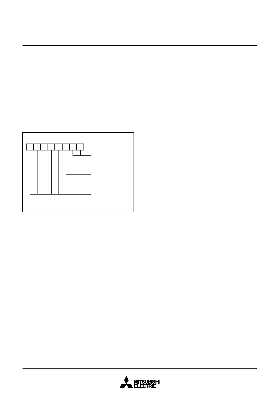
CPU mode register
The CPU mode register is allocated at address 003B
16
.
The CPU mode register contains the stack page selection bit.
Fig. 1 Structure of CPU mode register
CPU mode register
(
CPUM : address
003B
16
)
b7
b0
Stack page selection bit
0 : 0 page
1 : 1 page
Not used (return "0" when read)
Processor mode bits
b1 b0
0 0 : Single-chip mode
0 1 : Memory expansion mode
1 0 : Microprocessor mode
1 1 : Not available

MITSUBISHI MICROCOMPUTERS
3802 Group
SINGLE-CHIP 8-BIT CMOS MICROCOMPUTER
9
Memory
Special function register (SFR) area
The Special Function Register area in the zero page contains con-
trol registers such as I/O ports and timers.
RAM
RAM is used for data storage and for stack area of subroutine
calls and interrupts.
ROM
The first 128 bytes and the last 2 bytes of ROM are reserved for
device testing and the rest is user area for storing programs.
Interrupt vector area
The interrupt vector area contains reset and interrupt vectors.
Zero page
The 256 bytes from addresses 0000
16
to 00FF
16
are called the
zero page area. The internal RAM and the special function regis-
ters (SFR) are allocated to this area.
The zero page addressing mode can be used to specify memory
and register addresses in the zero page area. Access to this area
with only 2 bytes is possible in the zero page addressing mode.
Special page
The 256 bytes from addresses FF00
16
to FFFF
16
are called the
special page area. The special page addressing mode can be
used to specify memory addresses in the special page area. Ac-
cess to this area with only 2 bytes is possible in the special page
addressing mode.
Fig. 2 Memory map diagram
0100
16
0000
16
0040
16
0440
16
FF00
16
FFDC
16
FFFE
16
FFFF
16
192
256
384
512
640
768
896
1024
XXXX
16
00FF
16
013F
16
01BF
16
023F
16
02BF
16
033F
16
03BF
16
043F
16
4096
8192
12288
16384
20480
24576
28672
32768
F000
16
E000
16
D000
16
C000
16
B000
16
A000
16
9000
16
8000
16
F080
16
E080
16
D080
16
C080
16
B080
16
A080
16
9080
16
8080
16
YYYY
16
ZZZZ
16
RAM
ROM
Reserved area
SFR area
Not used
Interrupt vector area
ROM area
Reserved ROM area
(128 bytes)
Zero page
Special page
RAM area
RAM capacity
(bytes)
Address
XXXX
16
ROM capacity
(bytes)
Address
YYYY
16
Reserved ROM area
Address
ZZZZ
16
MITSUBISHI MICROCOMPUTERS
3802 Group
SINGLE-CHIP 8-BIT CMOS MICROCOMPUTER
10
Fig. 3 Memory map of special function register (SFR)
0020
16
0021
16
0022
16
0023
16
0024
16
0025
16
0026
16
0027
16
0028
16
0029
16
002A
16
002B
16
002C
16
002D
16
002E
16
002F
16
0030
16
0031
16
0032
16
0033
16
0034
16
0035
16
0036
16
0037
16
0038
16
0039
16
003A
16
003B
16
003C
16
003D
16
003E
16
003F
16
0000
16
0001
16
0002
16
0003
16
0004
16
0005
16
0006
16
0007
16
0008
16
0009
16
000A
16
000B
16
000C
16
000D
16
000E
16
000F
16
0010
16
0011
16
0012
16
0013
16
0014
16
0015
16
0016
16
0017
16
0018
16
0019
16
001A
16
001B
16
001C
16
001D
16
001E
16
001F
16
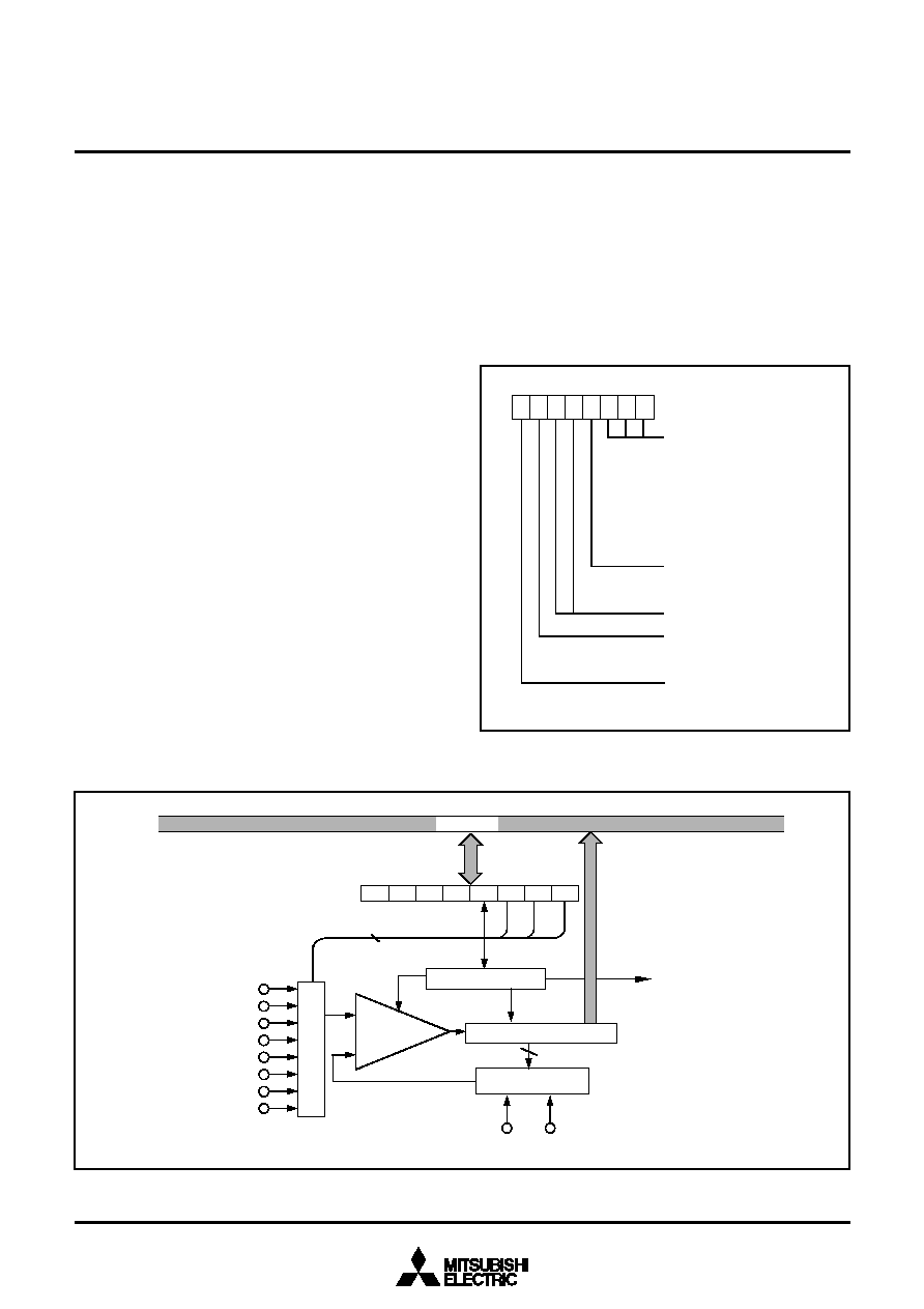
Serial I/O2 register (SIO2)
Port P0 (P0)
Port P0 direction register (P0D)
Port P1 (P1)
Port P1 direction register (P1D)
Port P2 (P2)
Port P2 direction register (P2D)
Port P3 (P3)
Port P3 direction register (P3D)
Port P4 (P4)
Port P4 direction register (P4D)
Port P5 (P5)
Port P5 direction register (P5D)
Port P6 (P6)
Port P6 direction register (P6D)
Transmit/Receive buffer register (TB/RB)
Serial I/O1 status register (SIO1STS)
Serial I/O1 control register (SIO1CON)
UART control register (UARTCON)
Baud rate generator (BRG)
Serial I/O2 control register (SIO2CON)
Interrupt control register 2(ICON2)
A-D conversion register (AD)
Prescaler Y (PREY)
Timer Y (TY)
AD/DA control register (ADCON)
D-A1 conversion register (DA1)
D-A2 conversion register (DA2)
Interrupt edge selection register
(INTEDGE)
CPU mode register (CPUM)
Interrupt request register 1(IREQ1)
Interrupt request register 2(IREQ2)
Interrupt control register 1(ICON1)
Prescaler 12 (PRE12)
Timer 2 (T2)
Prescaler X (PREX)
Timer X (TX)
Timer 1 (T1)
Timer XY mode register (TM)
PWM control register (PWMCON)
PMW prescaler (PREPWM)
PWM register (PWM)
MITSUBISHI MICROCOMPUTERS
3802 Group
SINGLE-CHIP 8-BIT CMOS MICROCOMPUTER
11
Related SFRs
CPU mode register
CPU mode register
CPU mode register
AD/DA control register
CPU mode register
CPU mode register
Interrupt edge selection
register
Serial I/O1 control
register
UART control register
Serial I/O2 control
register
Timer XY mode register
PWM control register
Interrupt edge selection register
Pin
P0
0
≠P0
7
P1
0
≠P1
7
P2
0
≠P2
7
P3
0
/DA
1
P3
1
/DA
2
P3
2
≠P3
7
P4
0
/INT
4
,
P4
1
/INT
0
,
P4
3
/INT
2
P4
4
/R
X
D,
P4
5
/T
X
D,
P4
6
/S
CLK1
,
P4
7
/S
RDY1
P5
0
/SIN
2
,
P5
1
/S
OUT2
,
P5
2
/S
CLK2
,
P5
3
/S
RDY2
P5
4
/CNTR
0
,
P5
5
/CNTR
1
P5
6
/PWM
P5
7
/INT
3
P6
0
/AN
0
≠
P6
7
/AN
7
Name
Port P0
Port P1
Port P2
Port P3
Port P4
Port P5
Port P6
Input/Output
Input/output,
individual bits
Input/output,
individual bits
Input/output,
individual bits
Input/output,
individual bits
Input/output,
individual bits
Input/output,
individual bits
Input/output,
individual bits
I/O Format
CMOS 3-state output
CMOS compatible
input level
CMOS 3-state output
CMOS compatible
input level
CMOS 3-state output
CMOS compatible
input level
CMOS 3-state output
CMOS compatible
input level
CMOS 3-state output
CMOS compatible
input level
CMOS 3-state output
CMOS compatible
input level
CMOS 3-state output
CMOS compatible
input level
Non-Port Function
Address low-order byte
output
Address high-order
byte output
Data bus I/O
D-A conversion output
Control signal I/O
External interrupt input
Serial I/O1 function I/O
Serial I/O2 function I/O
Timer X and Timer Y
function I/O
PWM output
External interrupt input
A-D conversion input
Ref.No.
(1)
(2)
(1)
(3)
(4)
(5)
(6)
(7)
(8)
(9)
(10)
(11)
(12)
(13)
(3)
(14)
Note 1: For details of the functions of ports P0 to P3 in modes other than single-chip mode, and how to use double-function ports as func-
tion I/O ports, refer to the applicable sections.
2: Make sure that the input level at each pin is either 0 V or V
CC
during execution of the STP instruction.
When an input level is at an intermediate potential, a current will flow from V
CC
to V
SS
through the input-stage gate.
I/O Ports
Direction registers
The 3802 group has 56 programmable I/O pins arranged in seven
I/O ports (ports P0 to P6). The I/O ports have direction registers
which determine the input/output direction of each individual pin.
Each bit in a direction register corresponds to one pin, each pin
can be set to be input port or output port.
When "0" is written to the bit corresponding to a pin, that pin be-
comes an input pin. When "1" is written to that bit, that pin be-
comes an output pin.
If data is read from a pin which is set to output, the value of the
port output latch is read, not the value of the pin itself. Pins set to
input are floating. If a pin set to input is written to, only the port
output latch is written to and the pin remains floating.

MITSUBISHI MICROCOMPUTERS
3802 Group
SINGLE-CHIP 8-BIT CMOS MICROCOMPUTER
12
Fig. 4 Port block diagram (single-chip mode) (1)
(1) Ports P0, P1, P2, P3
2
≠P3
7
Direction register
Data bus
Port latch
(2) Ports P3
0
, P3
1
(3) Ports P4
0≠
P4
3
, P5
7
Direction register
Data bus
Port latch
Serial I/O1 input
Serial I/O1 enable bit
Receive enable bit
(4) Port P4
4
(5) Port P4
5
(6) Port P4
6
Direction register
Data bus
Port latch
Serial I/O1 ready output
Serial I/O1 enable bit
S
RDY1
output enable bit
Serial I/O1 mode selection bit
(7) Port P4
7
(8) Port P5
0
Serial I/O2 input
Direction register
Data bus
Port latch
D≠A conversion output
DA
1
output enable bit (P3
0
)
DA
2
output enable bit (P3
1
)
Direction register
Data bus
Port latch
Interrupt input
Direction register
Data bus
Port latch
Serial I/O1 output
Serial I/O1 enable bit
Transmit enable bit
P4
5
/T
X
D P-channel output disable bit
Direction register
Data bus
Port latch
Serial I/O1 clock output
Serial I/O1 mode selection bit
Serial I/O1 enable bit
Serial I/O1 enable bit
Serial I/O1 synchronous
clock selection bit
Serial I/O1
external
clock input
Direction register
Data bus
Port latch

MITSUBISHI MICROCOMPUTERS
3802 Group
SINGLE-CHIP 8-BIT CMOS MICROCOMPUTER
13
Fig. 5 Port block diagram (single-chip mode) (2)
(14) Port P6
(13) Port P5
6
(12) Ports P5
4
, 5
5
(9) Port P5
1
(10) Port P5
2
(11) Port P5
3
Serial I/O2 transmit end signal
Serial I/O2 port selection bit
P5
1
/S
OUT2
P-channel output disable bit
Direction register
Data bus
Port latch
Serial I/O2 output
Serial I/O2 external clock input
Serial I/O2
synchronous clock selection bit
Serial I/O2 port selection bit
Direction register
Data bus
Port latch
Serial I/O2 clock output
Direction register
Data bus
Port latch
Serial I/O2 ready output
S
RDY2
output enable bit
Direction register
Data bus
Port latch
Pulse output mode
Timer output
CNTR
0
, CNTR
1
Interrupt input
Direction register
Data bus
Port latch
PWM output
PWM output enable bit
A-D conversion input
Direction register
Data bus
Port latch
Analog input pin selection bit
MITSUBISHI MICROCOMPUTERS
3802 Group
SINGLE-CHIP 8-BIT CMOS MICROCOMPUTER
14
INTERRUPTS
Interrupts occur by sixteen sources: seven external, eight internal,
and one software.
Interrupt control
Each interrupt is controlled by an interrupt request bit, an interrupt
enable bit, and the interrupt disable flag except for the software in-
terrupt set by the BRK instruction. An interrupt occurs if the corre-
sponding interrupt request and enable bits are "1" and the inter-
rupt disable flag is "0".
Interrupt enable bits can be set or cleared by software.
Interrupt request bits can be cleared by software, but cannot be
set by software.
The BRK instruction cannot be disabled with any flag or bit. The I
(interrupt disable) flag disables all interrupts except the BRK in-
struction interrupt.
When several interrupts occur at the same time, the interrupts are
received according to priority.
Interrupt operation
When an interrupt is received, the contents of the program counter
and processor status register are automatically stored into the
stack. The interrupt disable flag is set to inhibit other interrupts
from interfering.The corresponding interrupt request bit is cleared
and the interrupt jump destination address is read from the vector
table into the program counter.
Notes on use
When the active edge of an external interrupt (INT
0
to INT
4
,
CNTR
0
, or CNTR
1
) is changed, the corresponding interrupt re-
quest bit may also be set. Therefore, please take following se-
quence;
(1) Disable the external interrupt which is selected.
(2) Change the active edge selection.
(3) Clear the interrupt request bit which is selected to "0".
(4) Enable the external interrupt which is selected.
Interrupt Source
Reset (Note 2)
INT
0
INT
1
Serial I/O1
reception
Serial I/O1
transmission
Timer X
Timer Y
Timer 1
Timer 2
CNTR
0
CNTR
1
Serial I/O2
INT
2
INT
3
INT
4
A-D converter
BRK instruction
Low
FFFC
16
FFFA
16
FFF8
16
FFF6
16
FFF4
16
FFF2
16
FFF0
16
FFEE
16
FFEC
16
FFEA
16
FFE8
16
FFE6
16
FFE4
16
FFE2
16
FFE0
16
FFDE
16
FFDC
16
High
FFFD
16
FFFB
16
FFF9
16
FFF7
16
FFF5
16
FFF3
16
FFF1
16
FFEF
16
FFED
16
FFEB
16
FFE9
16
FFE7
16
FFE5
16
FFE3
16
FFE1
16
FFDF
16
FFDD
16
Table 1. Interrupt vector addresses and priority
Priority
1
2
3
4
5
6
7
8
9
10
11
12
13
14
15
16
17
Interrupt Request
Generating Conditions
At reset
At detection of either rising or
falling edge of INT
0
input
At detection of either rising or
falling edge of INT
1
input
At completion of serial I/O1
data reception
At completion of serial I/O1
transfer shift or when
transmission buffer is empty
At timer X underflow
At timer Y underflow
At timer 1 underflow
At timer 2 underflow
At detection of either rising or
falling edge of CNTR
0
input
At detection of either rising or
falling edge of CNTR
1
input
At completion of serial I/O2
data transfer
At detection of either rising or
falling edge of INT
2
input
At detection of either rising or
falling edge of INT
3
input
At detection of either rising or
falling edge of INT
4
input
At completion of A-D conversion
At BRK instruction execution
Remarks
Non-maskable
External interrupt
(active edge selectable)
External interrupt
(active edge selectable)
Valid when serial I/O1 is selected
Valid when serial I/O1 is selected
STP release timer underflow
External interrupt
(active edge selectable)
External interrupt
(active edge selectable)
Valid when serial I/O2 is selected
External interrupt
(active edge selectable)
External interrupt
(active edge selectable)
External interrupt
(active edge selectable)
Non-maskable software interrupt
Note 1: Vector addresses contain interrupt jump destination addresses.
2: Reset function in the same way as an interrupt with the highest priority.
Vector Addresses (Note 1)
MITSUBISHI MICROCOMPUTERS
3802 Group
SINGLE-CHIP 8-BIT CMOS MICROCOMPUTER
15
Fig. 6 Interrupt control
Fig. 7 Structure of interrupt-related registers
Interrupt disable flag (I)
Interrupt request
Interrupt request bit
Interrupt enable bit
BRK instruction
Reset
b7 b0
b7 b0
b7 b0
b7 b0
b7 b0
Interrupt edge selection register
INT
0
active edge selection bit
INT
1
active edge selection bit
Not used (returns "0" when read)
INT
2
active edge selection bit
INT
3
active edge selection bit
INT
4
active edge selection bit
Not used (returns "0" when read)
(INTEDGE : address 003A
16
)
Interrupt request register 1
INT
0
interrupt request bit
INT
1
interrupt request bit
Serial I/O1 receive interrupt request bit
Serial I/O1 transmit interrupt request bit
Timer X interrupt request bit
Timer Y interrupt request bit
Timer 1 interrupt request bit
Timer 2 interrupt request bit
Interrupt control register 1
INT
0
interrupt enable bit
INT
1
interrupt enable bit
Serial I/O1 receive interrupt enable bit
Serial I/O1 transmit interrupt enable bit
Timer X interrupt enable bit
Timer Y interrupt enable bit
Timer 1 interrupt enable bit
Timer 2 interrupt enable bit
0 : No interrupt request issued
1 : Interrupt request issued
(IREQ1 : address 003C
16
)
(ICON1 : address 003E
16
)
Interrupt request register 2
CNTR
0
interrupt request bit
CNTR
1
interrupt request bit
Serial I/O2 interrupt request bit
INT
2
interrupt request bit
INT
3
interrupt request bit
INT
4
interrupt request bit
AD converter interrupt request bit
Not used (returns "0" when read)
(IREQ2 : address 003D
16
)
Interrupt control register 2
CNTR
0
interrupt enable bit
CNTR
1
interrupt enable bit
Serial I/O2 interrupt enable bit
INT
2
interrupt enable bit
INT
3
interrupt enable bit
INT
4
interrupt enable bit
AD converter interrupt enable bit
Not used (returns "0" when read)
(Do not write "1" to this bit)
0 : Interrupts disabled
1 : Interrupts enabled
(ICON2 : address 003F
16
)
0 : Falling edge active
1 : Rising edge active
MITSUBISHI MICROCOMPUTERS
3802 Group
SINGLE-CHIP 8-BIT CMOS MICROCOMPUTER
16
Timer X count stop bit
0: Count start
1: Count stop
Timer XY mode register
(TM : address 0023
16)
Timer Y operating mode bit
0
0: Timer mode
0 1: Pulse output mode
1 0: Event counter mode
1 1: Pulse width measurement mode
CNTR
1
active edge switch bit
0: Interrupt at falling edge
Count at rising edge in event
counter mode
1: Interrupt at rising edge
Count at falling edge in event
counter mode
b7
CNTR
0
active edge switch bit
0: Interrupt at falling edge
Count at rising edge in event
counter mode
1: Interrupt at rising edge
Count at falling edge in event
counter mode
b0
Timer X operating mode bit
0
0: Timer mode
0 1: Pulse output mode
1 0: Event counter mode
1 1: Pulse width measurement mode
b1b0
b4b5
Timer Y count stop bit
0: Count start
1: Count stop
Timers
The 3802 group has four timers: timer X, timer Y, timer 1, and timer
2.
All timers are count down. When the timer reaches "00
16
", an un-
derflow occurs at the next count pulse and the corresponding
timer latch is reloaded into the timer and the count is continued.
When a timer underflows, the interrupt request bit corresponding
to that timer is set to "1".
The division ratio of each timer or prescaler is given by 1/(n + 1),
where n is the value in the corresponding timer or prescaler latch.
Timer 1 and Timer 2
The count source of prescaler 12 is the oscillation frequency di-
vided by 16. The output of prescaler 12 is counted by timer 1 and
timer 2, and a timer underflow sets the interrupt request bit.
Timer X and Timer Y
Timer X and Timer Y can each be selected in one of four operating
modes by setting the timer XY mode register.
Timer Mode
The timer counts f(X
IN
)/16 in timer mode.
Pulse Output Mode
Timer X (or timer Y) counts f(X
IN
)/16. Whenever the contents of
the timer reach "00
16
", the signal output from the CNTR
0
(or
CNTR
1
) pin is inverted. If the CNTR
0
(or CNTR
1
) active edge
switch bit is "0", output begins at " H".
If it is "1", output starts at "L". When using a timer in this mode, set
the corresponding port P5
4
( or port P5
5
) direction register to out-
put mode.
Event Counter Mode
Operation in event counter mode is the same as in timer mode,
except the timer counts signals input through the CNTR
0
or
CNTR
1
pin.
Pulse Width Measurement Mode
If the CNTR
0
(or CNTR
1
) active edge selection bit is "0", the timer
counts at the oscillation frequency divided by 16 while the CNTR
0
(or CNTR
1
) pin is at "H". If the CNTR
0
(or CNTR
1
) active edge
switch bit is "1", the count continues during the time that the
CNTR
0
(or CNTR
1
) pin is at "L".
In all of these modes, the count can be stopped by setting the
timer X (timer Y) count stop bit to "1". Every time a timer
underflows, the corresponding interrupt request bit is set.
Fig. 8 Structure of timer XY register
MITSUBISHI MICROCOMPUTERS
3802 Group
SINGLE-CHIP 8-BIT CMOS MICROCOMPUTER
17
Fig. 9 Block diagram of timer X, timer Y, timer 1, and timer 2
Timer X latch (8)
Timer X (8)
Prescaler X latch (8)
Prescaler X (8)
Oscillator
Divider
f(X
IN
)
1/16
CNTR
0
active
edge switch bit
P5
4
/CNTR
0
pin
Port P5
4
direction register
"0"
"1"
Event
counter
mode
Timer X count stop bit
CNTR
0
active
edge switch
bit
Port P5
4
latch
Pulse output
mode
Pulse width
measurement
mode
Timer mode
Pulse output
mode
"1"
"0"
Timer X latch write pulse
Pulse output mode
To timer X interrupt
request bit
To CNTR
0
interrupt
request bit
Data bus
Timer Y latch (8)
Timer Y (8)
Prescaler Y latch (8)
Prescaler Y (8)
CNTR
1
active
edge switch bit
P5
5
/CNTR
1
pin
Port P5
5
direction register
"0"
"1"
Event
counter
mode
Timer Y count stop bit
CNTR
1
active
edge switch
bit
Port P5
5
latch
Pulse output
mode
Pulse width
measurement
mode
Timer mode
Pulse output
mode
"1"
"0"
Timer Y latch write pulse
Pulse output mode
To timer Y interrupt
request bit
To CNTR
1
interrupt
request bit
Data bus
Q
Q
R
Toggle flip- flop
T
Q
Q
R
Toggle flip- flop
T
Timer 2 latch (8)
Timer 1 latch (8)
Prescaler
12 latch (8)
Prescaler 12 (8)
Timer 2 (8)
Timer 1 (8)
Data bus
To timer 2 interrupt
request bit
To timer 1 interrupt
request bit
MITSUBISHI MICROCOMPUTERS
3802 Group
SINGLE-CHIP 8-BIT CMOS MICROCOMPUTER
18
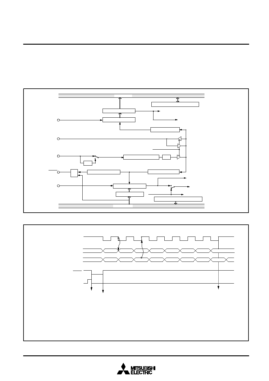
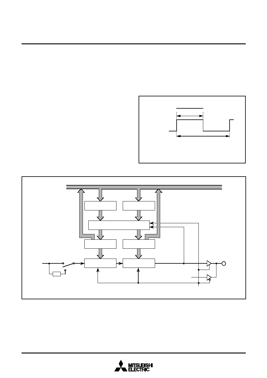
Serial I/O1
Serial I/O1 can be used as either clock synchronous or asynchro-
nous (UART) serial I/O. A dedicated timer is also provided for
baud rate generation.
Clock synchronous serial I/O mode
Clock synchronous serial I/O1 mode can be selected by setting
the mode selection bit of the serial I/O1 control register to "1".
For clock synchronous serial I/O1, the transmitter and the receiver
must use the same clock. If an internal clock is used, transfer is
started by a write signal to the TB/RB (address 0018
16
).
Fig. 10 Block diagram of clock synchronous serial I/O1
Fig. 11 Operation of clock synchronous serial I/O1 function
1/4
X
IN
1/4
F/F
P4
6
/S
CLK1
Serial I/O1 status register
Serial I/O1 control register
P4
7
/S
RDY1
P4
4
/R
X
D
P4
5
/T
X
D
f(X
IN
)
Receive buffer
Address 0018
16
Receive shift register
Receive buffer full flag (RBF)
Receive interrupt request (RI)
Clock control circuit
Shift clock
Serial I/O1 synchronous
clock selection bit
Frequency division ratio 1/(n+1)
Baud rate generator
Address 001C
16
BRG count source selection bit
Clock control circuit
Falling-edge detector
Transmit buffer
Data bus
Address 0018
16
Shift clock
Transmit shift completion flag (TSC)
Transmit buffer empty flag (TBE)
Transmit interrupt request (TI)
Transmit interrupt source selection bit
Address 0019
16
Data bus
Address 001A
16
Transmit shift register
D
7
D
7
D
0
D
1
D
2
D
3
D
4
D
5
D
6
D
0
D
1
D
2
D
3
D
4
D
5
D
6
RBF = 1
TSC = 1
TBE = 0
TBE = 1
TSC = 0
Transfer shift clock
(1/2 to 1/2048 of the internal
clock, or an external clock)
Serial output TxD
Serial input RxD
Write pulse to receive/transmit
buffer (address 0018
16
)
Overrun error (OE)
detection
Notes 1 : The transmit interrupt (TI) can be selected to occur either when the transmit buffer has emptied (TBE=1) or after the
transmit shift operation has ended (TSC=1), by setting the transmit interrupt source selection bit (TIC) of the serial I/O1
control register.
2 : If data is written to the transmit buffer when TSC=0, the transmit clock is generated continuously and serial data is
output continuously from the TxD pin.
3 : The receive interrupt (RI) is set when the receive buffer full flag (RBF) becomes "1" .
Receive enable signal
S
RDY1
MITSUBISHI MICROCOMPUTERS
3802 Group
SINGLE-CHIP 8-BIT CMOS MICROCOMPUTER
19
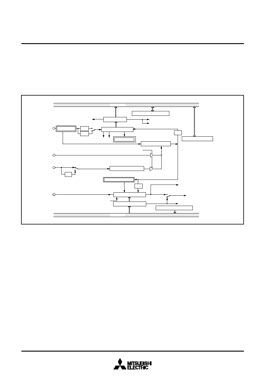
Asynchronous serial I/O (UART) mode
Clock asynchronous serial I/O mode (UART) can be selected by
clearing the serial I/O mode selection bit of the serial I/O control
register to "0".
Eight serial data transfer formats can be selected, and the transfer
formats used by a transmitter and receiver must be identical.
The transmit and receive shift registers each have a buffer, but the
two buffers have the same address in memory. Since the shift reg-
ister cannot be written to or read from directly, transmit data is
written to the transmit buffer, and receive data is read from the re-
ceive buffer.
The transmit buffer can also hold the next data to be transmitted,
and the receive buffer can hold a character while the next charac-
ter is being received.
Fig. 12 Block diagram of UART serial I/O
f(X
IN
)
1/4
OE
PE FE
1/16
1/16
Data bus
Receive buffer
Address 0018
16
Receive shift register
Receive buffer full flag (RBF)
Receive interrupt request (RI)
Baud rate generator
Frequency division ratio 1/(n+1)
Address 001C
16
ST/SP/PA generator
Transmit buffer
Data bus
Transmit shift register
Address
0018
16
Transmit shift completion flag (TSC)
Transmit buffer empty flag (TBE)
Transmit interrupt request (TI)
Address
0019
16
STdetector
SP detector
UART control register
Address 001B
16
Character length selection bit
Address 001A
16
BRG count source selection bit
Transmit interrupt source selection bit
Serial I/O1 synchronous clock selection bit
Clock control circuit
Character length selection bit
7 bits
8 bits
Serial I/O1 control register
P4
6
/S
CLK1
Serial I/O1 status register
P4
4
/R
X
D
P4
5
/T
X
D
MITSUBISHI MICROCOMPUTERS
3802 Group
SINGLE-CHIP 8-BIT CMOS MICROCOMPUTER
20
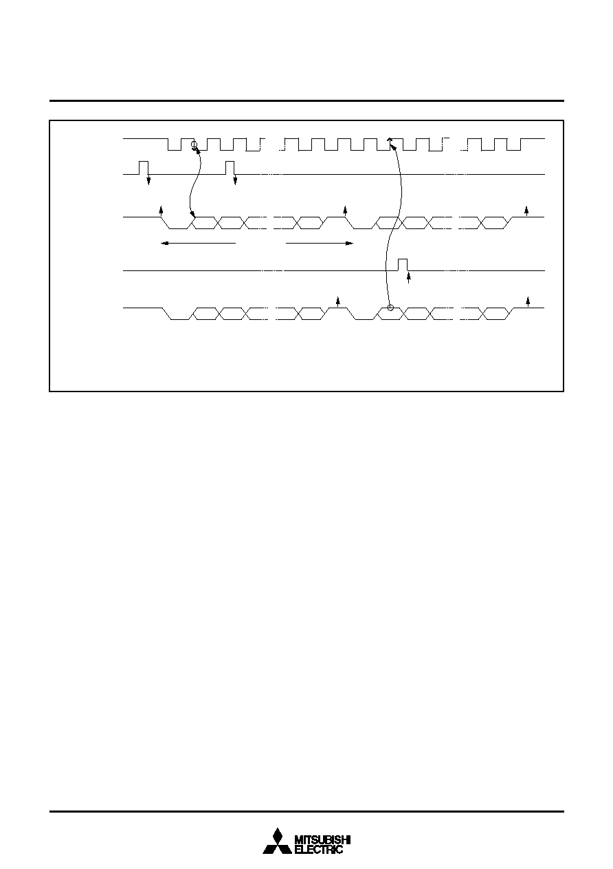
Fig. 13 Operation of UART serial I/O function
Serial I/O1 control register (SIO1CON) 001A
16
The serial I/O control register consists of eight control bits for the
serial I/O function.
UART control register (UARTCON) 001B
16
The UART control register consists of four control bits (bits 0 to 3)
which are valid when asynchronous serial I/O is selected and set
the data format of an data transfer. One bit in this register (bit 4) is
always valid and sets the output structure of the P4
5
/T
X
D pin.
Serial I/O1 status register (SIO1STS) 0019
16
The read-only serial I/O1 status register consists of seven flags
(bits 0 to 6) which indicate the operating status of the serial I/O
function and various errors.
Three of the flags (bits 4 to 6) are valid only in UART mode.
The receive buffer full flag (bit 1) is cleared to "0" when the receive
buffer is read.
If there is an error, it is detected at the same time that data is
transferred from the receive shift register to the receive buffer, and
the receive buffer full flag is set. A write to the serial I/O status reg-
ister clears all the error flags OE, PE, FE, and SE (bit 3 to bit 6, re-
spectively). Writing "0" to the serial I/O enable bit SIOE (bit 7 of
the Serial I/O Control Register) also clears all the status flags, in-
cluding the error flags.
All bits of the serial I/O1 status register are initialized to "0" at re-
set, but if the transmit enable bit (bit 4) of the serial I/O control reg-
ister has been set to "1", the transmit shift completion flag (bit 2)
and the transmit buffer empty flag (bit 0) become "1".
Transmit buffer/Receive buffer register (TB/
RB) 0018
16
The transmit buffer and the receive buffer are located at the same
address. The transmit buffer is write-only and the receive buffer is
read-only. If a character bit length is 7 bits, the MSB of data stored
in the receive buffer is "0".
Baud rate generator (BRG) 001C
16
The baud rate generator determines the baud rate for serial trans-
fer.
The baud rate generator divides the frequency of the count source
by 1/(n + 1), where n is the value written to the baud rate genera-
tor.
TSC=0
TBE=1
RBF=0
TBE=0
TBE=0
RBF=1
RBF=1
ST
D
0
D
1
SP
D
0
D
1
ST
SP
TBE=1
TSC=1
ST
D
0
D
1
SP
D
0
D
1
ST
SP
Transmit or receive clock
Transmit buffer write
signal
Generated at 2nd bit in 2-stop-bit mode
1 start bit
7 or 8 data bit
1 or 0 parity bit
1 or 2 stop bit (s)
1: Error flag detection occurs at the same time that the RBF flag becomes "1" (at 1st stop bit, during reception).
2: The transmit interrupt (TI) can be selected to occur when either the TBE or TSC flag becomes "1", depending on the setting of the transmit interrupt
source selection bit (TIC) of the serial I/O control register.
3: The receive interrupt (RI) is set when the RBF flag becomes "1".
4: After data is written to the transmit buffer when TSC=1, 0.5 to 1.5 cycles of the data shift cycle is necessary until changing to TSC=0.
Notes
V
V
Serial output T
X
D
Serial input R
X
D
Receive buffer read
signal

MITSUBISHI MICROCOMPUTERS
3802 Group
SINGLE-CHIP 8-BIT CMOS MICROCOMPUTER
21
b7
b7
Transmit buffer empty flag (TBE)
0: Buffer full
1: Buffer empty
Receive buffer full flag (RBF)
0: Buffer empty
1: Buffer full
Transmit shift completion flag (TSC)
0: Transmit shift in progress
1: Transmit shift completed
Overrun error flag (OE)
0: No error
1: Overrun error
Parity error flag (PE)
0: No error
1: Parity error
Framing error flag (FE)
0: No error
1: Framing error
Summing error flag (SE)
0: (OE) U (PE) U (FE)=0
1: (OE) U (PE) U (FE)=1
Not used (returns "1" when read)
Serial I/O1 status register
(SIO1STS : address 0019
16
)
Serial I/O1 control register
(SIO1CON : address 001A
16
)
b0
b0
BRG count source selection bit (CSS)
0: f(X
IN
)
1: f(X
IN
)/4
Serial I/O1 synchronous clock selection bit (SCS)
0: BRG output divided by 4 when clock synchronous
serial I/O is selected, BRG output divided by 16
when UART is selected.
1: External clock input when clock synchronous serial
I/O is selected, external clock input divided by 16
when UART is selected.
S
RDY1
output enable bit (SRDY)
0: P4
7
pin operates as ordinaly I/O pin
1: P4
7
pin operates as S
RDY1
output pin
Transmit interrupt source selection bit (TIC)
0: Interrupt when transmit buffer has emptied
1: Interrupt when transmit shift operation is completed
Transmit enable bit (TE)
0: Transmit disabled
1: Transmit enabled
Receive enable bit (RE)
0: Receive disabled
1: Receive enabled
Serial I/O1 mode selection bit (SIOM)
0: Asynchronous serial I/O (UART)
1: Clock synchronous serial I/O
Serial I/O enable bit (SIOE)
0: Serial I/O disabled
(pins P4
4
to P4
7
operate as ordinary I/O pins)
1: Serial I/O enabled
(pins P4
4
to P4
7
operate as serial I/O pins)
b7
UART control register
(UARTCON : address 001B
16
)
Character length selection bit (CHAS)
0: 8 bits
1: 7 bits
Parity enable bit (PARE)
0: Parity checking disabled
1: Parity checking enabled
Parity selection bit (PARS)
0: Even parity
1: Odd parity
Stop bit length selection bit (STPS)
0: 1 stop bit
1: 2 stop bits
P4
5
/T
X
D P-channel output disable bit (POFF)
0: CMOS output (in output mode)
1: N-channel open drain output (in output mode)
Not used (return "1" when read)
b0
Fig. 14 Structure of serial I/O control registers

MITSUBISHI MICROCOMPUTERS
3802 Group
SINGLE-CHIP 8-BIT CMOS MICROCOMPUTER
22
Serial I/O2
The serial I/O2 function can be used only for clock synchronous
serial I/O.
For clock synchronous serial I/O the transmitter and the receiver
must use the same clock. If the internal clock is used, transfer is
started by a write signal to the serial I/O2 register.
Serial I/O2 control register (SIO2CON) 001D
16
The serial I/O2 control register contains seven bits which control
various serial I/O functions.
Fig. 15 Structure of serial I/O2 control register
Fig. 16 Block diagram of serial I/O2 function
X
IN
"1"
"0"
"0"
"1"
"0"
"1"
S
RDY2
S
CLK2
"0"
"1"
1/8
1/16
1/32
1/64
1/128
1/256
Data bus
Serial I/O2
interrupt request
Serial I/O2 port selection bit
Serial I/O counter 2 (3)
Serial I/O shift register 2 (8)
Synchronization circuit
Serial I/O2 port selection bit
Serial I/O2 synchronous
clock selection bit
S
RDY2
output enable bit
External clock
Internal synchronous
clock selection bits
Divider
P5
3
latch
P5
3
/S
RDY2
P5
2
/S
CLK2
P5
1
/S
OUT2
P5
0
/S
IN2
P5
2
latch
P5
1
latch
Serial I/O2 control register
(SIO2CON : address 001D
16
)
b7
Internal synchronous clock selection bits
0 0 0: f(X
IN
)/8
0 0 1: f(X
IN
)/16
0 1 0: f(X
IN
)/32
0 1 1: f(X
IN
)/64
1 1 0: f(X
IN
)/128
1 1 1: f(X
IN
)/256
Serial I/O2 port selection bit (SM2
3
)
0: I/O port
1: S
OUT2
,S
CLK2
output pin
S
RDY2
output enable bit (SM2
4
)
0: I/O port
1: S
RDY2
output pin
Transfer direction selection bit (SM2
5
)
0: LSB first
1: MSB first
Serial I/O2 synchronous clock selection bit (SM2
6
)
0: External clock
1: Internal clock
P5
1
/S
OUT2
P-channel output disable bit
0: CMOS output (in output mode)
1: N-channel open-drain output (in output mode)
b0
b2 b1 b0
MITSUBISHI MICROCOMPUTERS
3802 Group
SINGLE-CHIP 8-BIT CMOS MICROCOMPUTER
23
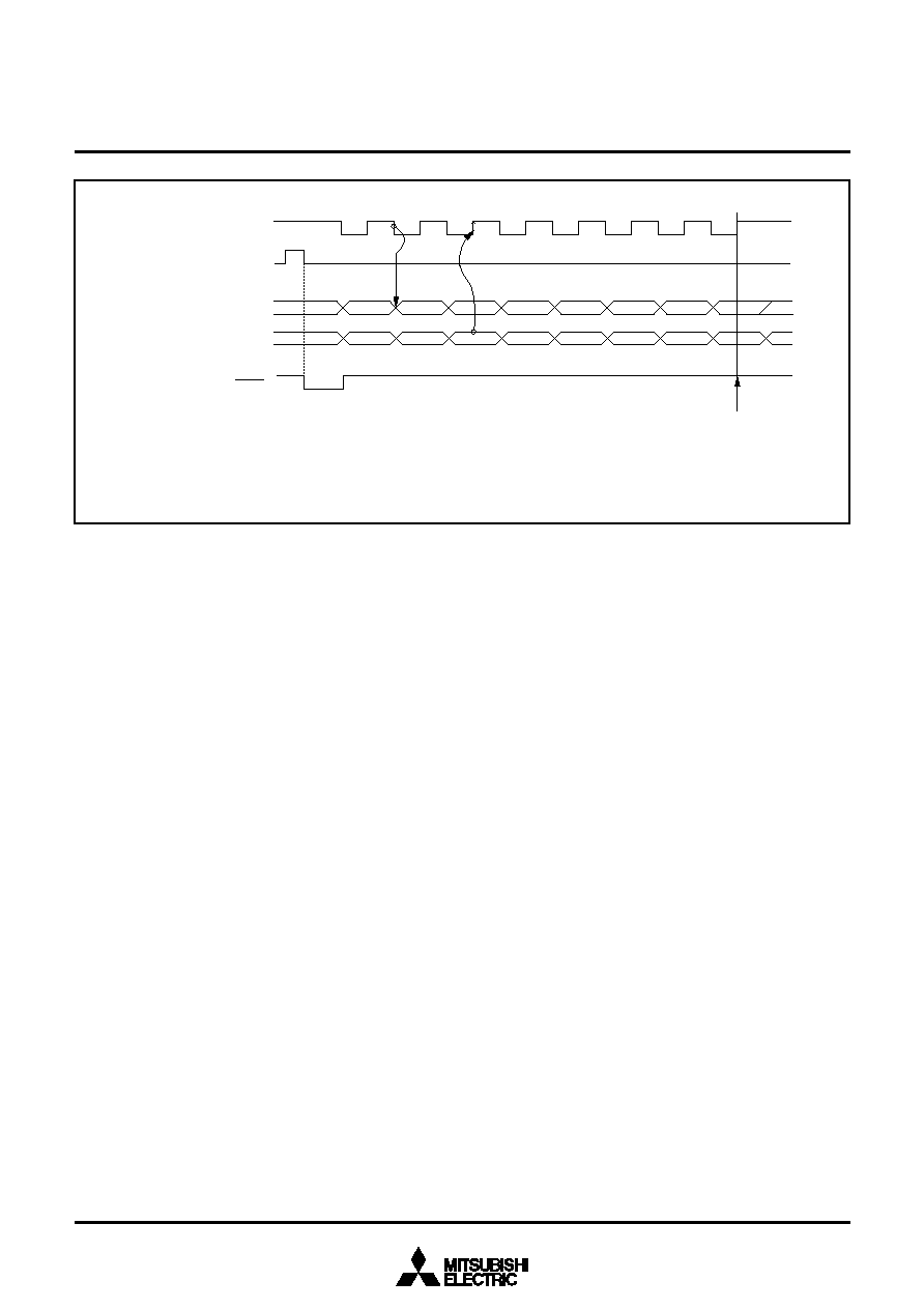
Fig. 17 Timing of serial I/O2 function
D
7
D
0
D
1
D
2
D
3
D
4
D
5
D
6
Transfer clock (Note 1)
Serial I/O2 output S
OUT2
Serial I/O2 input S
IN2
Receive enable signal S
RDY2
Serial I/O2 register
write signal
(Note 2)
Serial I/O2 interrupt request bit set
1: When the internal clock is selected as the transfer clock, the divide ratio can be selected by setting bits 0 to 2 of the serial
I/O2 control register.
2: When the internal clock is selected as the transfer clock, the S
OUT2
pin goes to high impedance after transfer completion.
Notes
MITSUBISHI MICROCOMPUTERS
3802 Group
SINGLE-CHIP 8-BIT CMOS MICROCOMPUTER
24
Data bus
Count source
selection bit
"0"
"1"
PWM
prescaler pre-latch
PWM
register pre-latch
PWM
prescaler latch
PWM
register latch
Transfer control circuit
PWM register
1/2
X
IN
Port P5
6
latch
PWM enable bit
Port P5
6
PWM prescaler
PULSE WIDTH MODULATION (PWM)
The 3802 group has a PWM function with an 8-bit resolution,
based on a signal that is the clock input X
IN
or that clock input di-
vided by 2.
Data Setting
The PWM output pin also functions as port P5
6
. Set the PWM pe-
riod by the PWM prescaler, and set the period during which the
output pulse is an "H" by the PWM register.
If the value in the PWM prescaler is n and the value in the PWM
register is m (where n = 0 to 255 and m = 0 to 255) :
PWM period = 255
!
(n+1)/f(X
IN
)
= 51
!
(n+1)
µ
s (when X
IN
= 5 MHz)
Output pulse "H" period = PWM period
!
m/255
= 0.2
!
(n+1)
!
m
µ
s
(when X
IN
= 5 MHz)
PWM Operation
When bit 0 (PWM enable bit) of the PWM control register is set to
"1", operation starts by initializing the PWM output circuit, and
pulses are output starting at an "H".
If the PWM register or PWM prescaler is updated during PWM
output, the pulses will change in the cycle after the one in which
the change was made.
Fig. 18 Timing of PWM cycle
Fig. 19 Block diagram of PWM function
51
!
m
!
(n+1)
255
µ
s
T = [51
!
(n+1)]
µ
s
PWM output
m: Contents of PWM register
n : Contents of PWM prescaler
T : PWM cycle (when X
IN
= 5
MHz)

MITSUBISHI MICROCOMPUTERS
3802 Group
SINGLE-CHIP 8-BIT CMOS MICROCOMPUTER
25
A
B
C
B
T
C
T2
=
PWM output
PWM register
write signal
PWM prescaler
write signal
(Changes from "A" to "B" during "H" period)
(Changes from "T" to "T2" during PWM period)
When the contents of the PWM register or PWM prescaler have changed, the PWM
output will change from the next period after the change.
T
T
T2
Fig. 20 Structure of PWM control register
Fig. 21 PWM output timing when PWM register or PWM prescaler is changed
PWM control register
(PWMCON : address 002B
16
)
PWM function enable bit
Count source selection bit
Not used (return "0" when read)
b7
b0
0: PWM disabled
1: PWM enabled
0: f(X
IN
)
1: f(X
IN
)/2
MITSUBISHI MICROCOMPUTERS
3802 Group
SINGLE-CHIP 8-BIT CMOS MICROCOMPUTER
26
A-D Converter
The functional blocks of the A-D converter are described below.
[A-D conversion register]
The A-D conversion register is a read-only register that stores the
result of an A-D conversion. When reading this register during an
A-D conversion, the previous conversion result is read.
[AD/DA control register]
The AD/DA control register controls the A-D conversion process.
Bits 0 to 2 select a specific analog input pin. Bit 3 signals the
completion of an A-D conversion. The value of this bit remains at
"0" during an A-D conversion, and changes to "1" when an A-D
conversion ends. Writing "0" to this bit starts the A-D conversion.
Bits 6 and 7 are used to control the output of the D-A converter.
[Comparison voltage generator]
The comparison voltage generator divides the voltage between
AV
SS
and V
REF
into 256, and outputs the divided voltages.
[Channel selector]
The channel selector selects one of the ports P6
0
/AN
0
to P6
7
/AN
7
,
and inputs the voltage to the comparator.
Fig.22 Structure of AD/DA control register
Fig. 23 Block diagram of A-D converter
[Comparator and Control circuit]
The comparator and control circuit compares an analog input volt-
age with the comparison voltage, then stores the result in the A-D
conversion register. When an A-D conversion is complete, the
control circuit sets the AD conversion completion bit and the AD
interrupt request bit to "1".
Note that the comparator is constructed linked to a capacitor, so
set f(X
IN
) to 500 kHz or more during an A-D conversion.
AD/DA control register
(ADCON : address 0034
16
)
Analog input pin selection bits
0 0 0: P6
0
/AN
0
0 0 1: P6
1
/AN
1
0 1 0: P6
2
/AN
2
0 1 1: P6
3
/AN
3
1 0 0: P6
4
/AN
4
1 0 1: P6
5
/AN
5
1 1 0: P6
6
/AN
6
1 1 1: P6
7
/AN
7
AD conversion completion bit
0: Conversion in progress
1: Conversion completed
Not used (return "0" When read)
DA
1
output enable bit
0: DA
1
output disabled
1: DA
1
output enabled
DA
2
output enable bit
0: DA
2
output disabled
1: DA
2
output enabled
b7
b0
b2 b1 b0
Channel selector
A-D control circuit
A-D conversion register
Resistor ladder
V
REF
AV
SS
Comparator
A-D interrupt request
b7
b0
3
8
P6
0
/AN
0
P6
1
/AN
1
P6
2
/AN
2
P6
3
/AN
3
P6
4
/AN
4
P6
5
/AN
5
P6
6
/AN
6
P6
7
/AN
7
Data bus
(Address 0035
16
)
AD/DA control register
(Address 0034
16
)
MITSUBISHI MICROCOMPUTERS
3802 Group
SINGLE-CHIP 8-BIT CMOS MICROCOMPUTER
27
D-A Converter
The 3802 group has two internal D-A converters (DA1 and DA2)
with 8-bit resolutions.
The D-A converter is performed by setting the value in the D-A
conversion register. The result of D-A converter is output from the
DA
1
or DA
2
pin by setting the DA output enable bit to "1".
When using the D-A converter, the corresponding port direction
register bit (P3
0
/DA
1
or P3
1
/DA
2
) should be set to "0" (input sta-
tus).
The output analog voltage V is determined by the value n (base
10) in the D-A conversion register as follows:
V = V
REF
!
n/256 (n = 0 to 255)
Where V
REF
is the reference voltage.
At reset, the D-A conversion registers are cleared to "00
16
", the DA
output enable bits are cleared to "0", and the P3
0
/DA
1
and P3
1
/
DA
2
pins are set to input (high impedance).
The D-A output is not buffered, so connect an external buffer when
driving a low-impedance load.
Set V
CC
to 3.0 V or more when using the D-A converter.
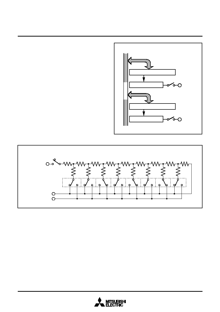
Fig. 24 Block diagram of D-A converter
Fig. 25 Equivalent connection circuit of D-A converter
P3
0
/DA
1
D-A1 conversion register (8)
R-2R resistor ladder
DA
1
output enable bit
P3
1
/DA
2
D-A2 conversion register (8)
R-2R resistor ladder
DA
2
output enable bit
Data bus
AV
SS
V
REF
"0"
"1"
MSB
"0"
"1"
R
2R
R
2R
R
2R
R
2R
R
2R
R
2R
R
2R
2R
LSB
2R
P3
0
/DA1
D-A1
conversion
register
DA
1
output enable bit
MITSUBISHI MICROCOMPUTERS
3802 Group
SINGLE-CHIP 8-BIT CMOS MICROCOMPUTER
28
Note.
!
: Undefined
V
: The initial values of CM
1
are determined by the level at the
CNV
SS
pin.
The contents of all other registers and RAM are undefined
after a reset, so they must be initialized by software.
Register contents
(0001
16
) ∑ ∑ ∑
Prescaler X
Port P0 direction register
Port P1 direction register
Port P2 direction register
Port P3 direction register
Port P4 direction register
Port P5 direction register
Port P6 direction register
Serial I/O1 status register
Serial I/O1 control register
Timer X
UART control register
Serial I/O2 control register
Prescaler 12
Timer 1
Timer XY mode register
(1)
(2)
(3)
(4)
(5)
(6)
(7)
(8)
(9)
(10)
(11)
(12)
(13)
(14)
(15)
(16)
(17)
(18)
(19)
(20)
(21)
(22)
(23)
(24)
(25)
(26)
(27)
(28)
(29)
(30)
(31)
(0003
16
) ∑ ∑ ∑
(0005
16
) ∑ ∑ ∑
(0007
16
) ∑ ∑ ∑
(0009
16
) ∑ ∑ ∑
(000B
16
) ∑ ∑ ∑
(000D
16
) ∑ ∑ ∑
(0019
16
) ∑ ∑ ∑
(001A
16
) ∑ ∑ ∑
(001B
16
) ∑ ∑ ∑
(001D
16
) ∑ ∑ ∑
(0020
16
) ∑ ∑ ∑
(0021
16
) ∑ ∑ ∑
(0022
16
) ∑ ∑ ∑
(0023
16
) ∑ ∑ ∑
(0024
16
) ∑ ∑ ∑
(0025
16
) ∑ ∑ ∑
(0026
16
) ∑ ∑ ∑
(0027
16
) ∑ ∑ ∑
(002B
16
) ∑ ∑ ∑
(0034
16
) ∑ ∑ ∑
(0036
16
) ∑ ∑ ∑
(0037
16
) ∑ ∑ ∑
(003A
16
) ∑ ∑ ∑
(003B
16
) ∑ ∑ ∑
(003C
16
) ∑ ∑ ∑
(003D
16
) ∑ ∑ ∑
(003E
16
) ∑ ∑ ∑
Address
Timer 2
Prescaler Y
Timer Y
PWM control register
AD/DA control register
D-A1 conversion register
D-A2 conversion register
Interrupt edge selection register
CPU mode register
Interrupt request register 1
Interrupt request register 2
Interrupt control register 1
Interrupt control register 2
Processor status register
Program counter
00
16
00
16
00
16
00
16
00
16
00
16
00
16
FF
16
FF
16
FF
16
FF
16
00
16
FF
16
01
16
00
16
00
16
00
16
1 1 1 0 0 0
0
0
00
16
00
16
00
16
Contents of address FFFC
16
! ! ! ! !
1
!
!
(PS)
(PC
H
)
(PC
L
)
Contents of address FFFD
16
00
16
00
16
00
16
(003F
16
) ∑ ∑ ∑
1 0 0 0 0 0
0
0
FF
16
0 0 0 0 1 0
0
0
00
16
0 0 0 0 0 0
0
V
Reset Circuit
To reset the microcomputer, the RESET pin should be held at an
"L" level for 2
µ
s or more. Then the RESET pin is returned to an "H"
level (the power source voltage should be between 4.0 V and 5.5
V), reset is released. Internal operation begin until after 8 to 13 X
IN
clock cycles are completed. After the reset is completed, the pro-
gram starts from the address contained in address FFFD
16
(high-
order byte) and address FFFC
16
(low-order byte).
Make sure that the reset input voltage is less than 0.6 V for V
CC
of
3.0 V (Extended operating temperature version : the reset input
voltage is less than 0.8 V for V
CC
of 4.0 V).
Fig. 27 Internal status of microcomputer after reset
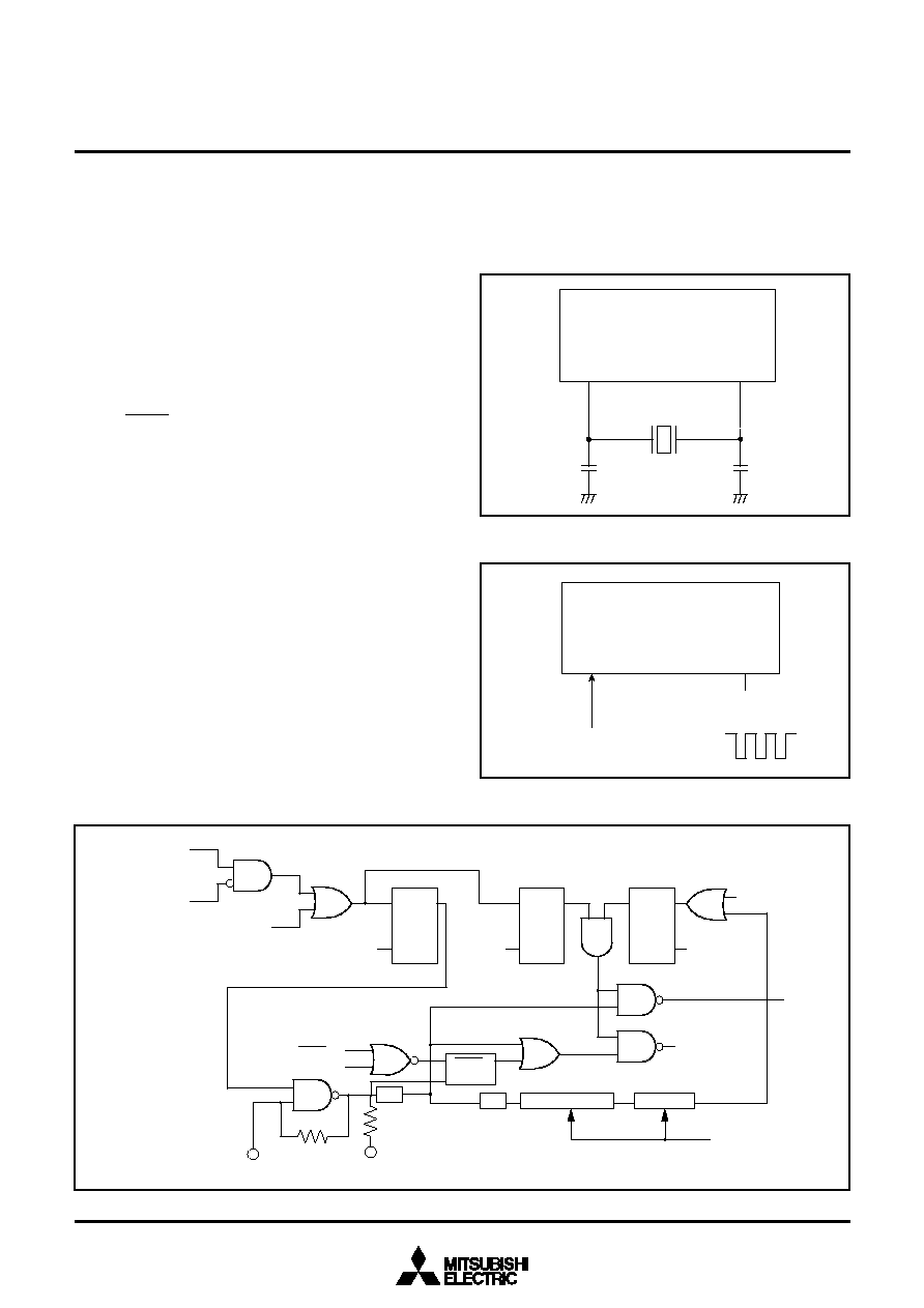
Fig. 26 Example of reset circuit
4.0V
0.8V
0V
0V
V
CC
RESET
Power source
voltage
Reset input
voltage
V
SS
M51953AL
4
5
1
3
0.1
µ
F
3802 group
MITSUBISHI MICROCOMPUTERS
3802 Group
SINGLE-CHIP 8-BIT CMOS MICROCOMPUTER
29
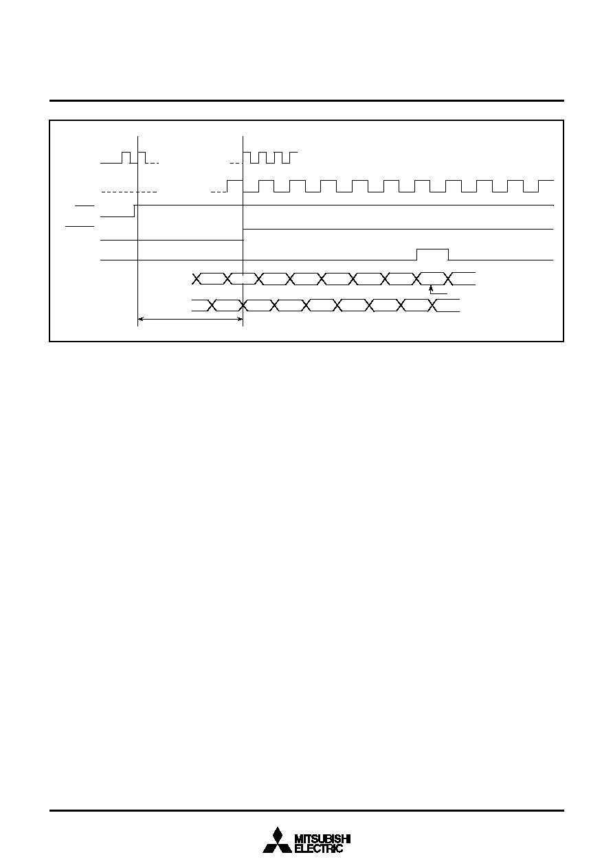
Fig. 28 Timing of reset
RESET
Data
Address
SYNC
X
IN
: 8 to 13 clock cycles
X
IN
?
?
?
?
?
FFFC
FFFD
AD
H
, AD
L
?
?
?
?
?
AD
L
AD
H
1: f(X
IN
) and f(
) are in the relationship: f(X
IN
)=2
∑
f(
).
2: A question mark (?) indicates an undefined status that depends on the previous status.
Reset address from the vector table
Notes
?
?
RESET
OUT
(internal reset)
MITSUBISHI MICROCOMPUTERS
3802 Group
SINGLE-CHIP 8-BIT CMOS MICROCOMPUTER
30
Clock Generating Circuit
An oscillation circuit can be formed by connecting a resonator be-
tween X
IN
and X
OUT
. To supply a clock signal externally, input it to
the X
IN
pin and make the X
OUT
pin open.
Oscillation control
Stop Mode
If the STP instruction is executed, the internal clock
stops at an
"H". Timer 1 is set to "01
16
" and prescaler 12 is set to "FF
16
".
Oscillator restarts when an external interrupt is received, but the
internal clock
remains at an "H" until timer 1 underflow.
This allows time for the clock circuit oscillation to stabilize.
If oscillator is restarted by a reset, no wait time is generated, so
keep the RESET pin at an "L" level until oscillation has stabilized.
Wait Mode
If the WIT instruction is executed, the internal clock
stops at an
"H" level, but the oscillator itself does not stop. The internal clock
restarts if a reset occurs or when an interrupt is received.
Since the oscillator does not stop, normal operation can be started
immediately after the clock is restarted.
To ensure that interrupts will be received to release the STP or
WIT state, interrupt enable bits must be set to "1" before the STP
or WIT instruction is executed.
When the STP status is released, prescaler 12 and timer 1 will
start counting and reset will not be released until timer 1
underflows, so set the timer 1 interrupt enable bit to "0" before the
STP instruction is executed.
Fig. 31 Block diagram of clock generating circuit
Fig. 30 External clock input circuit
Fig. 29 Ceramic resonator circuit
C
OUT
X
IN
X
OUT
C
IN
X
IN
X
OUT
Open
External oscillation
circuit
Vss
Vcc
1/8
X
OUT
X
IN
R
S
Q
STP instruction
WIT
instruction
R
S
Q
R
S
Q
Reset
STP instruction
Timer 1
ONW
control
Prescaler 12
1/2
output
Internal clock
Rd
Rf
ONW pin
Single-chip mode
Reset
Interrupt request
Interrupt disable
flag (I)
FF
16
01
16
Reset or STP instruction
MITSUBISHI MICROCOMPUTERS
3802 Group
SINGLE-CHIP 8-BIT CMOS MICROCOMPUTER
31
Processor Modes
Single-chip mode, memory expansion mode, and microprocessor
mode can be selected by changing the contents of the processor
mode bits CM
0
and CM
1
(bits 0 and 1 of address 003B
16
). In
memory expansion mode and microprocessor mode, memory can
be expanded externally through ports P0 to P3. In these modes,
ports P0 to P3 lose their I/O port functions and become bus pins.
Fig. 32 Memory maps in various processor modes
Fig. 33 Structure of CPU mode register
Single-Chip Mode
Select this mode by resetting the microcomputer with CNV
SS
con-
nected to V
SS
.
Memory Expansion Mode
Select this mode by setting the processor mode bits to "01" in soft-
ware with CNV
SS
connected to V
SS
. This mode enables external
memory expansion while maintaining the validity of the internal
ROM. Internal ROM will take precedence over external memory if
addresses conflict.
Microprocessor Mode
Select this mode by resetting the microcomputer with CNV
SS
con-
nected to V
CC
, or by setting the processor mode bits to "10" in
software with CNV
SS
connected to V
SS
. In microprocessor mode,
the internal ROM is no longer valid and external memory must be
used.
Port Name
Port P0
Port P1
Port P2
Port P3
Function
Outputs low-order byte of address.
Outputs high-order byte of address.
Operates as I/O pins for data D
7
to D
0
(including instruction codes).
P3
0
and P3
1
function only as output pins
(except that the port latch cannot be read).
P3
2
is the ONW input pin.
P3
3
is the RESET
OUT
output pin. (Note)
P3
4
is the
output pin.
P3
5
is the SYNC output pin.
P3
6
is the WR output pin, and P3
7
is the
RD output pin.
Note: If CNV
SS
is connected to V
SS
, the microcomputer goes to
single-chip mode after a reset, so this pin cannot be used
as the RESET
OUT
output pin.
Table 2.
Functions of ports in memory expansion mode and
microprocessor mode
0000
16
0040
16
0008
16
0000
16
YYYY
16
FFFF
16
0008
16
0040
16
FFFF
16
Internal RAM
reserved area
Internal ROM
Memory expansion mode
The shaded areas are external memory areas.
SFR area
:
YYYY
16
is the start address of internal ROM.
SFR area
Microprocessor mode
V
Internal RAM
reserved area
0440
16
V
0440
16
b0
CPU mode register
(CPUM : address 003B
16
)
Processor mode bits
0 0 : Single-chip mode
0 1 : Memory expansion mode
1 0 : Microprocessor mode
1 1 : Not available
Stack page selection bit
0 : 0 page
1 : 1 page
b7
Not used (return "0" when read)
b1 b0
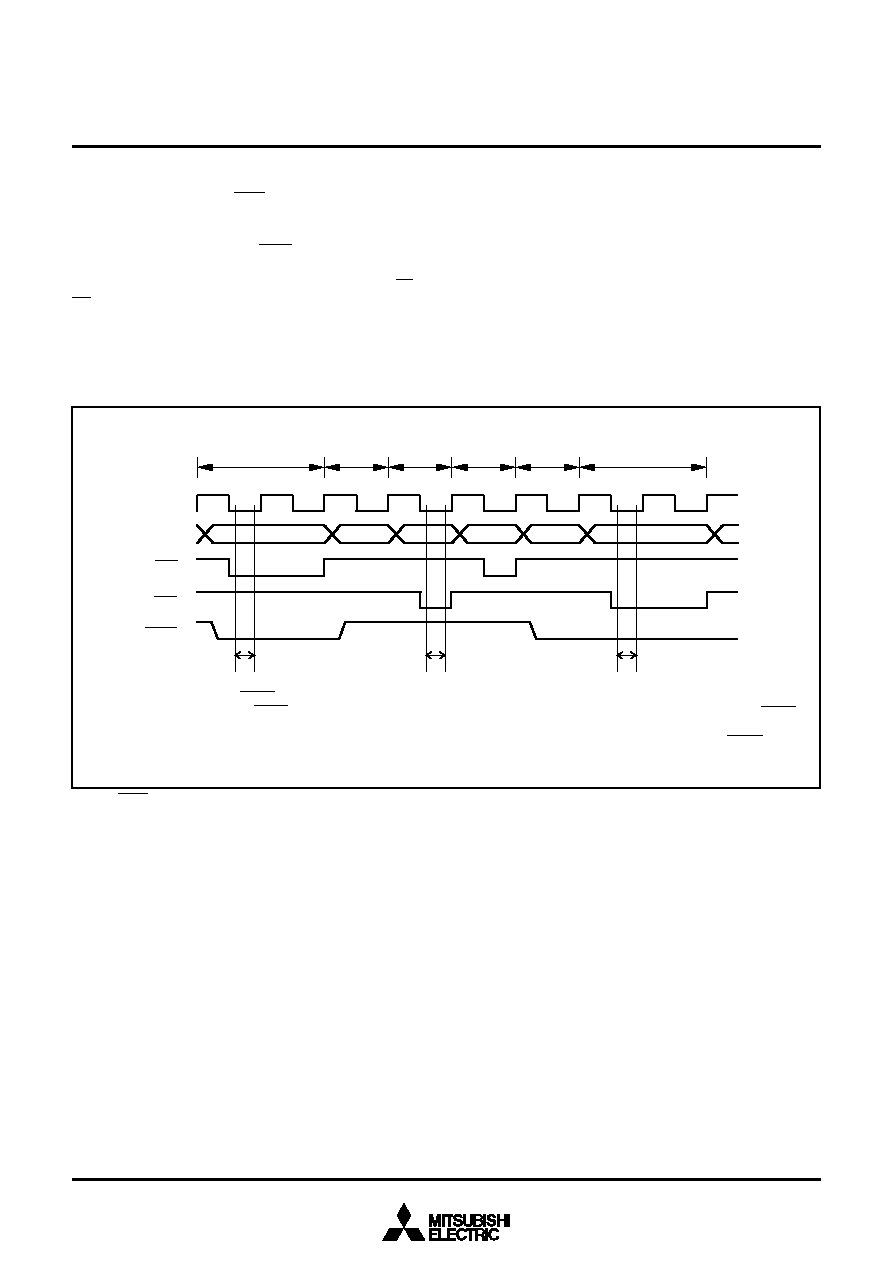
MITSUBISHI MICROCOMPUTERS
3802 Group
SINGLE-CHIP 8-BIT CMOS MICROCOMPUTER
32
Bus control with memory expansion
The 3802 group has a built-in ONW function to facilitate access to
external memory and I/O devices in memory expansion mode or
microprocessor mode.
If an "L" level signal is input to the ONW pin when the CPU is in a
read or write state, the corresponding read or write cycle is ex-
tended by one cycle of
. During this extended period, the RD or
WR signal remains at "L". This extension period is valid only for
writing to and reading from addresses 0000
16
to 0007
16
and
0440
16
to FFFF
16
in microprocessor mode, 0440
16
to YYYY
16
in
memory expansion mode, and only read and write cycles are ex-
tended.
Fig. 34 ONW function timing
Read cycle
Write cycle
Dummy cycle Write cycle
Read cycle Dummy cycle
AD
15
to AD
0
Period during which ONW input signal is received
During this period, the ONW signal must be fixed at either "H" or "L". At all other times, the input level of the ONW
signal has no affect on operations.
The bus cycles is not extended for an address in the area 0008
16
to 043F
16,
regardless of whether the ONW signal
is received.
V
:
V
V
V
ONW
WR
RD

MITSUBISHI MICROCOMPUTERS
3802 Group
SINGLE-CHIP 8-BIT CMOS MICROCOMPUTER
33
NOTES ON PROGRAMMING
Processor Status Register
The contents of the processor status register (PS) after a reset are
undefined, except for the interrupt disable flag (I) which is "1". Af-
ter a reset, initialize flags which affect program execution.
In particular, it is essential to initialize the index X mode (T) and
the decimal mode (D) flags because of their effect on calculations.
Interrupts
The contents of the interrupt request bits do not change immedi-
ately after they have been written. After writing to an interrupt re-
quest register, execute at least one instruction before executing a
BBC or BBS instruction.
Decimal Calculations
To calculate in decimal notation, set the decimal mode flag (D) to
"1", then execute an ADC or SBC instruction. Only the ADC and
SBC instructions yield proper decimal results. After executing an
ADC or SBC instruction, execute at least one instruction before
executing a SEC, CLC, or CLD instruction.
In decimal mode, the values of the negative (N), overflow (V), and
zero (Z) flags are invalid.
The carry flag can be used to indicate whether a carry or borrow
has occurred. Initialize the carry flag before each calculation.
Clear the carry flag before an ADC and set the flag before an
SBC.
Timers
If a value n (between 0 and 255) is written to a timer latch, the fre-
quency division ratio is 1/(n + 1).
Multiplication and Division Instructions
The index X mode (T) and the decimal mode (D) flags do not af-
fect the MUL and DIV instruction.
The execution of these instructions does not change the contents
of the processor status register.
Ports
The contents of the port direction registers cannot be read.
The following cannot be used:
∑ The data transfer instruction (LDA, etc.)
∑ The operation instruction when the index X mode flag (T) is "1"
∑ The addressing mode which uses the value of a direction regis-
ter as an index
∑ The bit-test instruction (BBC or BBS, etc.) to a direction register
∑ The read-modify-write instruction (ROR, CLB, or SEB, etc.) to a
direction register
Use instructions such as LDM and STA, etc., to set the port direc-
tion registers.
Serial I/O
In clock synchronous serial I/O, if the receive side is using an ex-
ternal clock and it is to output the S
RDY1
signal, set the transmit
enable bit, the receive enable bit, and the S
RDY1
output enable bit
to "1".
Serial I/O1 continues to output the final bit from the T
X
D pin after
transmission is completed. The S
OUT2
pin from serial I/O2 goes to
high impedance after transmission is completed.
A-D Converter
The comparator uses internal capacitors whose charge will be lost
if the clock frequency is too low.
Make sure that f(X
IN
) is at least 500 kHz during an A-D conver-
sion. (If the ONW pin has been set to "L", the A-D conversion will
take twice as long to match the longer bus cycle, and so f(X
IN
)
must be at least 1 MHz.)
Do not execute the STP or WIT instruction during an A-D conver-
sion.
D-A Converter
The accuracy of the D-A converter becomes poor rapidly under
the V
CC
= 3.0 V or less condition.
Instruction Execution Time
The instruction execution time is obtained by multiplying the fre-
quency of the internal clock
by the number of cycles needed to
execute an instruction.
The number of cycles required to execute an instruction is shown
in the list of machine instructions.
The frequency of the internal clock
is half of the X
IN
frequency.
When the ONW function is used in modes other than single-chip
mode, the frequency of the internal clock
may be one fourth the
X
IN
frequency.
Memory Expansion Mode
The memory expansion mode is not available in the following mi-
crocomputers.
∑ M38024M6-XXXSP
∑ M38024M6-XXXFP
Memory Expansion Mode and Microproces-
sor Mode
Execute the LDM or STA instruction for writing to port P3 (address
0006
16
) in memory expansion mode and microprocessor mode.
Set areas which can be read out and write to port P3 (address
0006
16
) in a memory, using the read-modify-write instruction
(SEB, CLB).
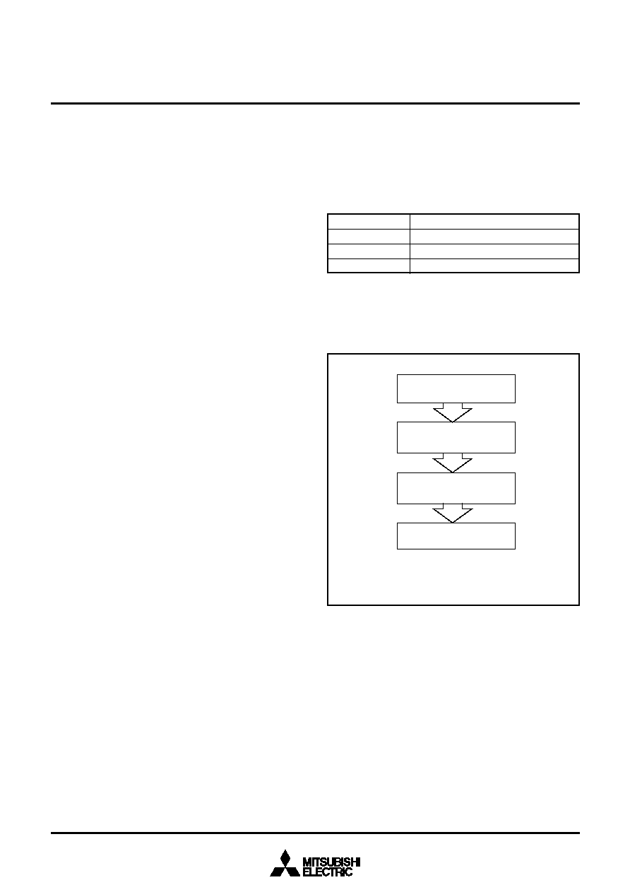
MITSUBISHI MICROCOMPUTERS
3802 Group
SINGLE-CHIP 8-BIT CMOS MICROCOMPUTER
34
DATA REQUIRED FOR MASK ORDERS
The following are necessary when ordering a mask ROM produc-
tion:
1. Mask ROM Order Confirmation Form
2. Mark Specification Form
3. Data to be written to ROM, in EPROM form (three identical
copies)
ROM PROGRAMMING METHOD
The built-in PROM of the blank One Time PROM version and built-
in EPROM version can be read or programmed with a general-
purpose PROM programmer using a special programming
adapter. Set the address of PROM programmer in the user ROM
area.
The PROM of the blank One Time PROM version is not tested or
screened in the assembly process and following processes. To en-
sure proper operation after programming, the procedure shown in
Figure 35 is recommended to verify programming.
Fig. 35 Programming and testing of One Time PROM version
Package
64P4B, 64S1B
64P6N
64D0
Name of Programming Adapter
PCA4738S-64A
PCA4738F-64A
PCA4738L-64A
Programming with PROM
programmer
Screening (Caution)
(150
∞
C for 40 hours)
Verification with
PROM programmer
Functional check in
target device
The screening temperature is far higher
than the storage temperature. Never
expose to 150
∞
C exceeding 100 hours.
Caution :

MITSUBISHI MICROCOMPUTERS
SINGLE-CHIP 8-BIT CMOS MICROCOMPUTER
3802 Group
35
ABSOLUTE MAXIMUM RATINGS
Power source voltage
Input voltage
P0
0
≠P0
7
, P1
0
≠P1
7
, P2
0
≠P2
7
,
P3
0
≠P3
7
, P4
0
≠P4
7
, P5
0
≠P5
7
,
P6
0
≠P6
7
,
V
REF
Input voltage
RESET, X
IN
Input voltage
CNV
SS
Output voltage P0
0
≠P0
7
, P1
0
≠P1
7
, P2
0
≠P2
7
,
P3
0
≠P3
7
, P4
0
≠P4
7
, P5
0
≠P5
7
,
P6
0
≠P6
7
,
X
OUT
Power dissipation
Operating temperature
Storage temperature
V
CC
V
I
V
I
V
I
V
O
P
d
T
opr
T
stg
Symbol
Parameter
Conditions
Ratings
≠0.3 to 7.0
≠0.3 to V
CC
+0.3
≠0.3 to V
CC
+0.3
≠0.3 to 13
≠0.3 to V
CC
+0.3
1000 (Note)
≠20 to 85
≠40 to 125
V
V
V
V
V
mW
∞
C
∞
C
Unit
T
a
= 25
∞
C
All voltages are based on V
SS
.
Output transistors are cut off.
RECOMMENDED OPERATING CONDITIONS
(Vcc = 3.0 to 5.5 V, Ta = ≠20 to 85
∞
C, unless otherwise noted)
Note 1: The minimum power source voltage is [V] (f(X
IN
) = XMHz) on the condition of 2 MHz < f(X
IN
) < 8 MHz.
2: The total output current is the sum of all the currents flowing through all the applicable ports. The total average current is an aver-
age value measured over 100 ms. The total peak current is the peak value of all the currents.
3: The peak output current is the peak current flowing in each port.
4: The average output current I
OL(avg)
, I
OH(avg)
in an average value measured over 100 ms.
5.5
5.5
V
CC
V
CC
V
CC
V
CC
V
CC
0.2 V
CC
0.2 V
CC
0.16 V
CC
≠80
≠80
80
80
≠40
≠40
40
40
≠10
10
≠5
5
8
6 V
CC
≠16
Power source voltage (f(X
IN
) < 2 MHz) (Note 1)
Power source voltage (f(X
IN
) = 8 MHz) (Note 1)
Power source voltage
Analog reference voltage (when A-D converter is used)
Analog reference voltage (when D-A converter is used)
Analog power source voltage
Analog input voltage
AN
0
≠AN
7
"H" input voltage
P0
0
≠P0
7
, P1
0
≠P1
7
, P2
0
≠P2
7
, P3
0
≠P3
7
, P4
0
≠P4
7
,
P5
0
≠P5
7
, P6
0
≠P6
7
"H" input voltage
RESET, X
IN
, CNV
SS
"L" input voltage
P0
0
≠P0
7
, P1
0
≠P1
7
, P2
0
≠P2
7
, P3
0
≠P3
7
, P4
0
≠P4
7
,
P5
0
≠P5
7
, P6
0
≠P6
7
"L" input voltage
RESET, CNV
SS
"L" input voltage
X
IN
"H" total peak output current
P0
0
≠P0
7
, P1
0
≠P1
7
, P2
0
≠P2
7
, P3
0
≠P3
7
(Note 2)
"H" total peak output current
P4
0
≠P4
7
,P5
0
≠P5
7
, P6
0
≠P6
7
(Note 2)
"L" total peak output current
P0
0
≠P0
7
, P1
0
≠P1
7
, P2
0
≠P2
7
, P3
0
≠P3
7
(Note 2)
"L" total peak output current
P4
0
≠P4
7
,P5
0
≠P5
7
, P6
0
≠P6
7
(Note 2)
"H" total average output current P0
0
≠P0
7
, P1
0
≠P1
7
, P2
0
≠P2
7
, P3
0
≠P3
7
(Note 2)
"H" total average output current P4
0
≠P4
7
,P5
0
≠P5
7
, P6
0
≠P6
7
(Note 2)
"L" total average output current
P0
0
≠P0
7
, P1
0
≠P1
7
, P2
0
≠P2
7
, P3
0
≠P3
7
(Note 2)
"L" total average output current
P4
0
≠P4
7
,P5
0
≠P5
7
, P6
0
≠P6
7
(Note 2)
"H" peak output current
P0
0
≠P0
7
, P1
0
≠P1
7
, P2
0
≠P2
7
, P3
0
≠P3
7
, P4
0
≠P4
7
,
P5
0
≠P5
7
, P6
0
≠P6
7
(Note 3)
"L" peak output current
P0
0
≠P0
7
, P1
0
≠P1
7
, P2
0
≠P2
7
, P3
0
≠P3
7
, P4
0
≠P4
7
,
P5
0
≠P5
7
, P6
0
≠P6
7
(Note 3)
"H" average output current
P0
0
≠P0
7
, P1
0
≠P1
7
, P2
0
≠P2
7
, P3
0
≠P3
7
, P4
0
≠P4
7
,
P5
0
≠P5
7
, P6
0
≠P6
7
(Note 4)
"L" average output current
P0
0
≠P0
7
, P1
0
≠P1
7
, P2
0
≠P2
7
, P3
0
≠P3
7
, P4
0
≠P4
7
,
P5
0
≠P5
7
, P6
0
≠P6
7
(Note 4)
Internal clock oscillation frequency (V
CC
= 4.0 to 5.5 V)
Internal clock oscillation frequency (V
CC
= 3.0 to 4.0 V)
V
CC
V
SS
V
REF
AV
SS
V
IA
V
IH
V
IH
V
IL
V
IL
V
IL
I
OH(peak)
I
OH(peak)
I
OL(peak)
I
OL(peak)
I
OH(avg)
I
OH(avg)
I
OL(avg)
I
OL(avg)
I
OH(peak)
I
OL(peak)
I
OH(avg)
I
OL(avg)
f(X
IN
)
Symbol
Parameter
Limits
Min.
V
V
V
V
V
V
V
V
V
V
mA
mA
mA
mA
mA
mA
mA
mA
mA
mA
mA
mA
MHz
Unit
3.0
4.0
2.0
3.0
AV
SS
0.8 V
CC
0.8 V
CC
0
0
0
5.0
5.0
0
0
Typ.
Max.
X + 16
6
Note: 300 mW in case of the flat package.
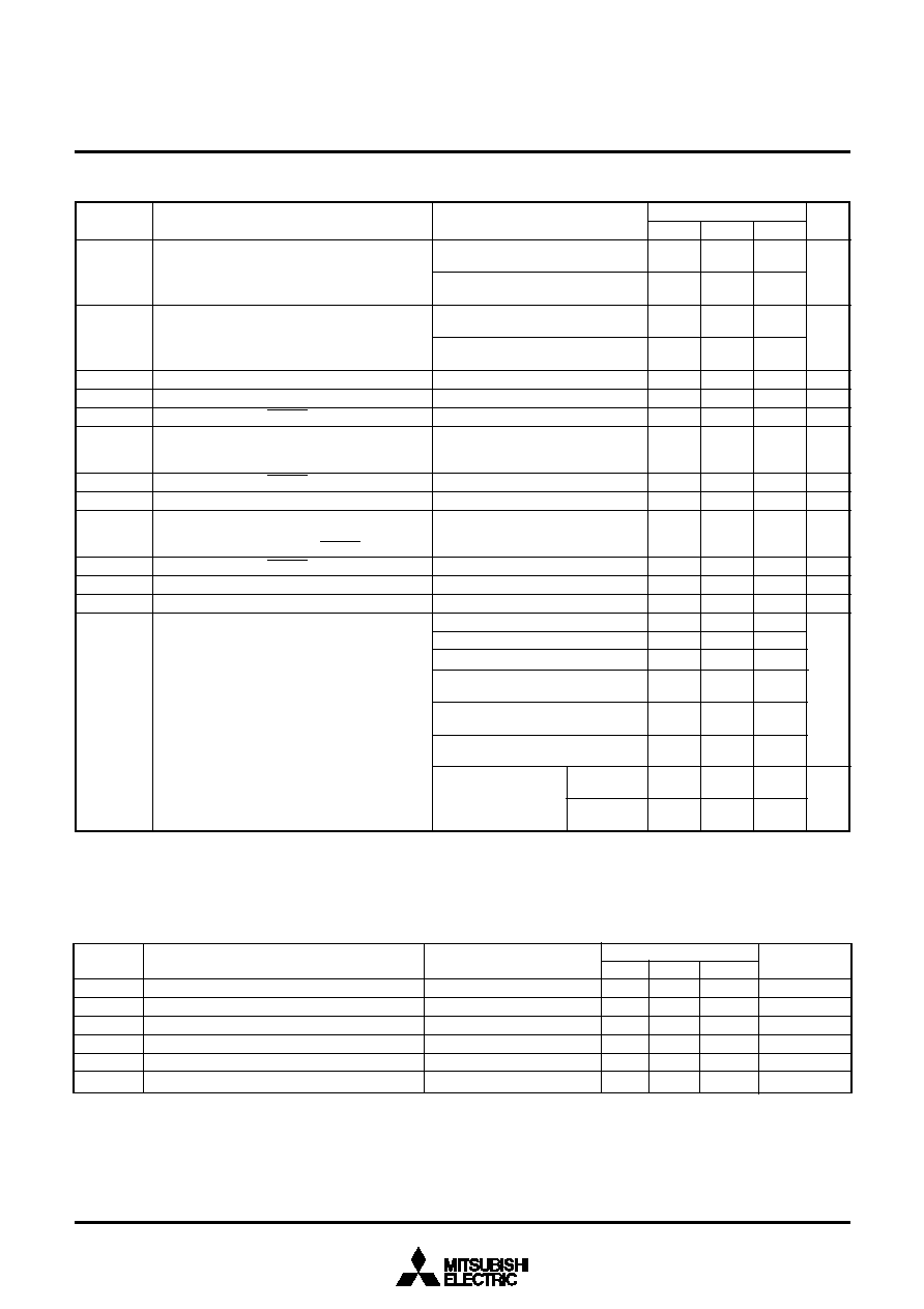
MITSUBISHI MICROCOMPUTERS
SINGLE-CHIP 8-BIT CMOS MICROCOMPUTER
3802 Group
36
When STP instruction
is executed with clock
stopped, output
transistors isolated.
Note 1: P4
5
is measured when the P4
5
/T
X
D P-channel output disable bit of the UART control register (bit 4 of address 001B
16
) is "0".
P5
1
is measured when the P5
1
/S
OUT2
P-channel output disable bit of the serial I/O2 control register (bit 7 of address 001D
16
) is "0".
2: With output transistors isolated and A-D converter having completed conversion, and not including current flowing through V
REF
pin.
2.0
1.0
5.0
5.0
≠5.0
≠5.0
5.5
13
8
2.0
1
10
"H" output voltage P0
0
≠P0
7
, P1
0
≠P1
7
, P2
0
≠P2
7
,
P3
0
≠P3
7
, P4
0
≠P4
7
, P5
0
≠P5
7
,
P6
0
≠P6
7
(Note 1)
"L" output voltage
P0
0
≠P0
7
, P1
0
≠P1
7
, P2
0
≠P2
7
,
P3
0
≠P3
7
, P4
0
≠P4
7
,P5
0
≠P5
7
,
P6
0
≠P6
7
Hysteresis
CNTR
0
, CNTR
1
, INT
0
≠INT
4
Hysteresis
R
X
D, S
CLK1
, S
IN2
, S
CLK2
Hysteresis
RESET
"H" input current
P0
0
≠P0
7
, P1
0
≠P1
7
, P2
0
≠P2
7
,
P3
0
≠P3
7
, P4
0
≠P4
7
, P5
0
≠P5
7
,
P6
0
≠P6
7
"H" input current
RESET, CNV
SS
"H" input current
X
IN
"L" input current
P0
0
≠P0
7
, P1
0
≠P1
7
, P2
0
≠P2
7
,
P3
0
≠P3
7
, P4
0
≠P4
7
, P5
0
≠P5
7
,
P6
0
≠P6
7
, RESET, CNV
SS
"L" input current
RESET, CNV
SS
"L" input current
X
IN
RAM hold voltage
Symbol
Parameter
Limits
Min.
V
Unit
V
CC
≠2.0
V
CC
≠1.0
0.4
0.5
0.5
4
≠4
6.4
4
0.8
1.5
1
0.2
0.1
Typ.
Max.
I
OH
= ≠10 mA
V
CC
= 4.0 to 5.5 V
I
OH
= ≠1.0 mA
V
CC
= 3.0 to 5.5 V
I
OL
= 10 mA
V
CC
= 4.0 to 5.5 V
I
OL
= 1.0 mA
V
CC
= 3.0 to 5.5 V
V
I
= V
CC
V
I
= V
CC
V
I
= V
CC
V
I
= V
SS
V
I
= V
SS
V
I
= V
SS
When clock stopped
f(X
IN
) = 8 MHz, V
CC
= 5 V
f(X
IN
) = 5 MHz, V
CC
= 5 V
f(X
IN
) = 2 MHz, V
CC
= 3 V
T
a
= 25
∞
C
(Note 2)
T
a
= 85
∞
C
(Note 2)
2.0
Test conditions
V
T+
≠ V
T≠
V
T+
≠ V
T≠
V
T+
≠ V
T≠
I
IH
I
IH
I
IH
I
IL
I
IL
I
IL
V
RAM
V
OH
V
OL
I
CC
V
V
V
V
µ
A
µ
A
µ
A
µ
A
µ
A
µ
A
V
mA
µ
A
Power source current
When WIT instruction is executed with
f(Xin) = 8MHz,V
CC
=5V
When WIT instruction is executed with
f(Xin) = 5MHz,V
CC
=5V
When WIT instruction is executed with
f(Xin) = 2MHz,V
CC
=3V
8
±
2.5
50
200
5.0
Limits
Min.
Bits
LSB
t
C
(
)
k
µ
A
µ
A
Typ.
Max.
±
1
35
150
0.5
Note: When D-A conversion registers (addresses 0036
16
and 0037
16
) contain "00
16
".
Resolution
Absolute accuracy (excluding quantization error)
Conversion time
Ladder resistor
Reference power source input current (Note)
A-D port input current
--
--
t
CONV
R
LADDER
I
VREF
I
I(AD)
Symbol
Parameter
Unit
V
REF
= 5.0 V
50
ELECTRICAL CHARACTERISTICS
(V
CC
= 3.0 to 5.5 V, V
SS
= 0 V, T
a
= ≠20 to 85
∞
C, unless otherwise noted)
Test conditions
A≠D CONVERTER CHARACTERISTICS
(V
CC
= 3.0 to 5.5 V, V
SS
= AV
SS
= 0 V, V
REF
= 2.0 V to V
CC
, T
a
= ≠20 to 85
∞
C, unless otherwise noted)

MITSUBISHI MICROCOMPUTERS
SINGLE-CHIP 8-BIT CMOS MICROCOMPUTER
3802 Group
37
Note: Using one D-A converter, with the value in the D-A conversion register of the other D-A converter being "00
16
", and excluding cur-
rents flowing through the A-D resistance ladder.
8
1.0
2.5
3
4
3.2
Resolution
Absolute accuracy
V
CC
= 4.0 to 5.5 V
V
CC
= 3.0 to 4.0 V
Setting time
Output resistor
Reference power source input current (Note)
--
--
t
su
R
O
I
VREF
Symbol
Parameter
Limits
Min.
Bits
%
µ
s
k
mA
Unit
1
Typ.
Max.
Test conditions
2.5
D-A CONVERTER CHARACTERISTICS
(V
CC
= 3.0 to 5.5 V, V
SS
= AV
SS
= 0 V, V
REF
= 3.0 V to V
CC
, T
a
= ≠20 to 85
∞
C, unless otherwise noted)
MITSUBISHI MICROCOMPUTERS
SINGLE-CHIP 8-BIT CMOS MICROCOMPUTER
3802 Group
38
Note: When f(X
IN
) = 8 MHz and bit 6 of address 001A
16
is "1". Divide this value by four when f(X
IN
) = 8 MHz and bit 6 of address 001A
16
is "0".
Reset input "L" pulse width
External clock input cycle time
External clock input "H" pulse width
External clock input "L" pulse width
CNTR
0
, CNTR
1
input cycle time
CNTR
0
, CNTR
1
input "H" pulse width
INT
0
to INT
4
input "H" pulse width
CNTR
0
, CNTR
1
input "L" pulse width
INT
0
to INT
4
input "L" pulse width
Serial I/O1 clock input cycle time (Note)
Serial I/O2 clock input cycle time
Serial I/O1 clock input "H" pulse width (Note)
Serial I/O2 clock input "H" pulse width
Serial I/O1 clock input "L" pulse width (Note)
Serial I/O2 clock input "L" pulse width
Serial I/O1 input set up time
Serial I/O2 input set up time
Serial I/O1 input hold time
Serial I/O2 input hold time
t
w(RESET)
t
c(X
IN
)
t
wH(X
IN
)
t
wL(X
IN
)
t
c(CNTR)
t
wH(CNTR)
t
wH(INT)
t
wL(CNTR)
t
wL(INT)
t
c(S
CLK1
)
t
c(S
CLK2
)
t
wH(S
CLK1
)
t
wH(S
CLK2
)
t
wL(S
CLK1
)
t
wL(S
CLK2
)
t
su(R
X
D≠S
CLK1
)
t
su(S
IN2
≠S
CLK2
)
t
h(S
CLK1
≠R
X
D)
t
h(S
CLK2
≠S
IN2
)
Symbol
Parameter
Limits
Min.
µ
s
ns
ns
ns
ns
ns
ns
ns
ns
ns
ns
ns
ns
ns
ns
ns
ns
ns
ns
Unit
TIMING REQUIREMENTS 1
(V
CC
= 4.0 to 5.5 V, V
SS =
0 V, T
a
= ≠20 to 85
∞
C, unless otherwise noted)
2
125
50
50
200
80
80
80
80
800
1000
370
400
370
400
220
200
100
200
Typ.
Max.
Reset input "L" pulse width
External clock input cycle time
External clock input "H" pulse width
External clock input "L" pulse width
CNTR
0
, CNTR
1
input cycle time
CNTR
0
, CNTR
1
input "H" pulse width
INT
0
to INT
4
input "H" pulse width
CNTR
0
, CNTR
1
input "L" pulse width
INT
0
to INT
4
input "L" pulse width
Serial I/O1 clock input cycle time (Note)
Serial I/O2 clock input cycle time
Serial I/O1 clock input "H" pulse width (Note)
Serial I/O2 clock input "H" pulse width
Serial I/O1 clock input "L" pulse width (Note)
Serial I/O2 clock input "L" pulse width
Serial I/O1 input set up time
Serial I/O2 input set up time
Serial I/O1 input hold time
Serial I/O2 input hold time
t
w(RESET)
t
c(X
IN
)
t
wH(X
IN
)
t
wL(X
IN
)
t
c(CNTR)
t
wH(CNTR)
t
wH(INT)
t
wL(CNTR)
t
wL(INT)
t
c(S
CLK1
)
t
c(S
CLK2
)
t
wH(S
CLK1
)
t
wH(S
CLK2
)
t
wL(S
CLK1
)
t
wL(S
CLK2
)
t
su(R
X
D≠S
CLK1
)
t
su(S
IN2
≠S
CLK2
)
t
h(S
CLK1
≠R
X
D)
t
h(S
CLK2
≠S
IN2
)
Symbol
Parameter
Limits
Min.
µ
s
ns
ns
ns
ns
ns
ns
ns
ns
ns
ns
ns
ns
ns
ns
ns
ns
ns
ns
Unit
TIMING REQUIREMENTS 2
(V
CC
= 3.0 to 5.5 V, V
SS =
0 V, T
a
= ≠20 to 85
∞
C, unless otherwise noted)
2
500/
(3 V
CC
≠8)
200/
(3 V
CC
≠8)
200/
(3 V
CC
≠8)
500
230
230
230
230
2000
2000
950
950
950
950
400
400
200
300
Typ.
Max.
Note: When f(X
IN
) = 2 MHz and bit 6 of address 001A
16
is "1". Divide this value by four when f(X
IN
) = 2 MHz and bit 6 of address 001A
16
is "0".
MITSUBISHI MICROCOMPUTERS
SINGLE-CHIP 8-BIT CMOS MICROCOMPUTER
3802 Group
39
Serial I/O1 clock output "H" pulse width
Serial I/O2 clock output "H" pulse width
Serial I/O1 clock output "L" pulse width
Serial I/O2 clock output "L" pulse width
Serial I/O1 output delay time (Note 1)
Serial I/O2 output delay time (Note 2)
Serial I/O1 output valid time (Note 1)
Serial I/O2 output valid time (Note 2)
Serial I/O1 clock output rising time
Serial I/O1 clock output falling time
Serial I/O2 clock output rising time
Serial I/O2 clock output falling time
CMOS output rising time (Note 3)
CMOS output falling time (Note 3)
140
200
30
30
30
40
30
30
Symbol
Parameter
Limits
Min.
ns
ns
ns
ns
ns
ns
ns
ns
ns
ns
ns
ns
ns
ns
Unit
SWITCHING CHARACTERISTICS 1
(V
CC
= 4.0 to 5.5 V, V
SS =
0 V, T
a
= ≠20 to 85
∞
C, unless otherwise noted)
t
c(S
CLK1
)/2≠30
t
c(S
CLK2
)/2≠160
t
c(S
CLK1
)/2≠30
t
c(S
CLK2
)/2≠160
≠30
0
10
10
Typ.
Max.
t
wH(S
CLK1
)
t
wH(S
CLK2
)
t
wL(S
CLK1
)
t
wL(S
CLK2
)
t
d(S
CLK1
≠T
X
D)
t
d(S
CLK2
≠S
OUT2
)
t
v(S
CLK1
≠T
X
D)
t
v(S
CLK2
≠S
OUT2
)
t
r(S
CLK1
)
t
f(S
CLK1
)
t
r(S
CLK2
)
t
f(S
CLK2
)
t
r(CMOS)
t
f(CMOS)
Test conditions
Fig. 36
Note1: When the P4
5
/T
X
D P-channel output disable bit of the UART control register (bit 4 of address 001B
16
) is "0".
2: When the P5
1
/S
OUT2
P-channel output disable bit of the serial I/O2 control register (bit 7 of address 001D
16
) is "0".
3: X
OUT
pin is excluded.
SWITCHING CHARACTERISTICS 2
(V
CC
= 3.0 to 5.5 V, V
SS =
0 V, T
a
= ≠20 to 85
∞
C, unless otherwise noted)
Serial I/O1 clock output "H" pulse width
Serial I/O2 clock output "H" pulse width
Serial I/O1 clock output "L" pulse width
Serial I/O2 clock output "L" pulse width
Serial I/O1 output delay time (Note 1)
Serial I/O2 output delay time (Note 2)
Serial I/O1 output valid time (Note 1)
Serial I/O2 output valid time (Note 2)
Serial I/O1 clock output rising time
Serial I/O1 clock output falling time
Serial I/O2 clock output rising time
Serial I/O2 clock output falling time
CMOS output rising time (Note 3)
CMOS output falling time (Note 3)
350
400
50
50
50
50
50
50
Symbol
Parameter
Limits
Min.
ns
ns
ns
ns
ns
ns
ns
ns
ns
ns
ns
ns
ns
ns
Unit
t
c(S
CLK1
)/2≠50
t
c(S
CLK2
)/2≠240
t
c(S
CLK1
)/2≠50
t
c(S
CLK2
)/2≠240
≠30
0
20
20
Typ.
Max.
t
wH(S
CLK1
)
t
wH(S
CLK2
)
t
wL(S
CLK1
)
t
wL(S
CLK2
)
t
d(S
CLK1
≠T
X
D)
t
d(S
CLK2
≠S
OUT2
)
t
v(S
CLK1
≠T
X
D)
t
v(S
CLK2
≠S
OUT2
)
t
r(S
CLK1
)
t
f(S
CLK1
)
t
r(S
CLK2
)
t
f(S
CLK2
)
t
r(CMOS)
t
f(CMOS)
Test conditions
Fig. 36
Note1: When the P4
5
/T
X
D P-channel output disable bit of the UART control register (bit 4 of address 001B
16
) is "0".
2: When the P5
1
/S
OUT2
P-channel output disable bit of the serial I/O2 control register (bit 7 of address 001D
16
) is "0".
3: X
OUT
pin is excluded.

MITSUBISHI MICROCOMPUTERS
SINGLE-CHIP 8-BIT CMOS MICROCOMPUTER
3802 Group
40
Note 1: The RESET
OUT
output goes "H" in sync with the rise of the
clock that is anywhere between about 8 cycle and 13 cycles after
the RESET input goes "H".
Before
ONW input set up time
After
ONW input hold time
Before
data bus set up time
After
data bus hold time
Before RD ONW input set up time
Before WR ONW input set up time
After RD ONW input hold time
After WR ONW input hold time
Before RD data bus set up time
After RD data bus hold time
t
su(ONW≠
)
t
h(
≠ONW)
t
su(DB≠
)
t
h(
≠DB)
t
su(ONW≠RD)
t
su(ONW≠WR)
t
h(RD≠ONW)
t
h(WR≠ONW)
t
su(DB≠RD)
t
h(RD≠DB)
Symbol
Parameter
Limits
Min.
ns
ns
ns
ns
ns
ns
ns
ns
Unit
≠20
≠20
60
0
≠20
≠20
65
0
Typ.
Max.
clock cycle time
clock "H" pulse width
clock "L" pulse width
After
AD
15
≠AD
8
delay time
After
AD
15
≠AD
8
valid time
After
AD
7
≠AD
0
delay time
After
AD
7
≠AD
0
valid time
SYNC delay time
SYNC valid time
RD and WR delay time
RD and WR valid time
After
data bus delay time
After
data bus valid time
RD pulse width, WR pulse width
RD pulse width, WR pulse width
(When one-wait is valid)
After AD
15
≠AD
8
RD delay time
After AD
15
≠AD
8
WR delay time
After AD
7
≠AD
0
RD delay time
After AD
7
≠AD
0
WR delay time
After RD AD
15
≠AD
8
valid time
After WR AD
15
≠AD
8
valid time
After RD AD
7
≠AD
0
valid time
After WR AD
7
≠AD
0
valid time
After WR data bus delay time
After WR data bus valid time
RESET
OUT
output delay time (Note 1)
RESET
OUT
output valid time (Note 1)
40
45
20
10
70
65
200
200
Symbol
Parameter
Limits
Min.
ns
ns
ns
ns
ns
ns
ns
ns
ns
ns
ns
ns
ns
ns
ns
ns
ns
ns
ns
ns
ns
ns
ns
Unit
t
c(X
IN
)
≠10
t
c(X
IN
)
≠10
6
6
3
15
t
c(X
IN
)
≠10
3t
c(X
IN
)
≠10
t
c(X
IN
)
≠35
t
c(X
IN
)
≠40
0
0
10
0
2t
c(X
IN
)
20
10
25
10
20
10
10
5
20
t
c(X
IN
)
≠15
t
c(X
IN
)
≠20
5
5
15
Typ.
Max.
t
c(
)
t
wH(
)
t
wL(
)
t
d(
≠AH)
t
v(
≠AH)
t
d(
≠AL)
t
v(
≠AL)
t
d(
≠SYNC)
t
v(
≠SYNC)
t
d(
≠WR)
t
v(
≠WR)
t
d(
≠DB)
t
v(
≠DB)
t
wL(RD)
t
wL(WR)
t
d(AH≠RD)
t
d(AH≠WR)
t
d(AL≠RD)
t
d(AL≠WR)
t
v(RD≠AH)
t
v(WR≠AH)
t
v(RD≠AL)
t
v(WR≠AL)
t
d(WR≠DB)
t
v(WR≠DB)
t
d(RESET≠RESET
OUT
)
t
v(
≠RESET)
Test conditions
Fig. 36
TIMING REQUIREMENTS 1 IN MEMORY EXPANSION MODE AND MICROPROCESSOR MODE
(V
CC
= 4.0 to 5.5 V, V
SS =
0 V, T
a
= ≠20 to 85
∞
C, unless otherwise noted)
SWITCHING CHARATERISTICS 1 IN MEMORY EXPANSION MODE AND MICROPROCESSOR MODE
(V
CC
= 4.0 to 5.5 V, V
SS =
0 V, T
a
= ≠20 to 85
∞
C, unless otherwise noted)
MITSUBISHI MICROCOMPUTERS
SINGLE-CHIP 8-BIT CMOS MICROCOMPUTER
3802 Group
41
Before
ONW input set up time
After
ONW input hold time
Before
data bus set up time
After
data bus hold time
Before RD ONW input set up time
Before WR ONW input set up time
After RD ONW input hold time
After WR ONW input hold time
Before RD data bus set up time
After RD data bus hold time
t
su(ONW≠
)
t
h(
≠ONW)
t
su(DB≠
)
t
h(
≠DB)
t
su(ONW≠RD)
t
su(ONW≠WR)
th
(RD≠ONW)
t
h(WR≠ONW)
t
su(DB≠RD)
t
h(RD≠DB)
Symbol
Parameter
Limits
Min.
ns
ns
ns
ns
Unit
≠20
≠20
180
0
≠20
≠20
185
0
Typ.
Max.
clock cycle time
clock "H" pulse width
clock "L" pulse width
After
AD
15
≠AD
8
delay time
After
AD
15
≠AD
8
valid time
After
AD
7
≠AD
0
delay time
After
AD
7
≠AD
0
valid time
SYNC delay time
SYNC valid time
RD and WR delay time
RD and WR valid time
After
data bus delay time
After
data bus valid time
RD pulse width, WR pulse width
RD pulse width, WR pulse width
(when one-wait is valid)
After AD
15
≠AD
8
RD delay time
After AD
15
≠AD
8
WR delay time
After AD
7
≠AD
0
RD delay time
After AD
7
≠AD
0
WR delay time
After RD AD
15
≠AD
8
valid time
After WR AD
15
≠AD
8
valid time
After RD AD
7
≠AD
0
valid time
After WR AD
7
≠AD
0
valid time
After WR data bus delay time
After WR data bus valid time
RESET
OUT
output delay time (Note 1)
RESET
OUT
output valid time (Note 1)
Symbol
Parameter
Limits
Min.
ns
ns
ns
ns
ns
ns
ns
ns
ns
ns
ns
ns
ns
ns
ns
ns
ns
ns
ns
ns
ns
ns
Unit
t
c(X
IN
)
≠20
t
c(X
IN
)
≠20
10
10
3
15
t
c(X
IN
)
≠20
3t
c(X
IN
)
≠20
t
c(X
IN
)
≠145
t
c(X
IN
)
≠145
5
5
10
0
2t
c(X
IN
)
15
15
40
20
15
7
10
10
Typ.
Max.
t
c(
)
t
wH(
)
t
wL(
)
t
d(
≠AH)
t
v(
≠AH)
t
d(
≠AL)
t
v(
≠AL)
t
d(
≠SYNC)
t
v(
≠SYNC)
t
d(
≠WR)
t
v(
≠WR)
t
d(
≠DB)
t
v(
≠DB)
t
wL(RD)
t
wL(WR)
t
d(AH≠RD)
t
d(AH≠WR)
t
d(AL≠RD)
t
d(AL≠WR)
t
v(RD≠AH)
t
v(WR≠AH)
t
v(RD≠AL)
t
v(WR≠AL)
t
d(WR≠DB)
t
v(WR≠DB)
t
d(RESET≠RESET
OUT
)
t
v(
≠RESET)
Test conditions
Fig. 36
Note1: The RESET
OUT
output goes "H" in sync with the fall of the
clock that is anywhere between about 8 cycle and 13 cycles after
the RESET input goes "H".
TIMING REQUIREMENTS 2 IN MEMORY EXPANSION MODE AND MICROPROCESSOR MODE
(V
CC
= 3.0 V, V
SS =
0 V, T
a
= ≠20 to 85
∞
C, unless otherwise noted)
SWITCHING CHARACTERISTICS 2 IN MEMORY EXPANSION MODE AND MICROPROCESSOR MODE
(V
CC
= 3.0 V, V
SS =
0 V, T
a
= ≠20 to 85
∞
C, unless otherwise noted)
ns
ns
ns
ns
ns
150
150
25
15
200
195
300
300

MITSUBISHI MICROCOMPUTERS
SINGLE-CHIP 8-BIT CMOS MICROCOMPUTER
3802 Group
42
Power source voltage
Input voltage
P0
0
≠P0
7
, P1
0
≠P1
7
, P2
0
≠P2
7
,
P3
0
≠P3
7
, P4
0
≠P4
7
, P5
0
≠P5
7
,
P6
0
≠P6
7
,
V
REF
Input voltage
RESET, X
IN
Input voltage
CNV
SS
Output voltage P0
0
≠P0
7
, P1
0
≠P1
7
, P2
0
≠P2
7
,
P3
0
≠P3
7
, P4
0
≠P4
7
, P5
0
≠P5
7
,
P6
0
≠P6
7
,
X
OUT
Power dissipation
Operating temperature
Storage temperature
V
CC
V
I
V
I
V
I
V
O
P
d
T
opr
T
stg
Symbol
Parameter
Conditions
Ratings
≠0.3 to 7.0
≠0.3 to V
CC
+0.3
≠0.3 to V
CC
+0.3
≠0.3 to 13
≠0.3 to V
CC
+0.3
1000 (Note)
≠40 to 85
≠65 to 150
V
V
V
V
V
mW
∞
C
∞
C
Unit
T
a
= 25
∞
C
All voltage are based on V
SS
.
Output transistors are cut off.
Note 1: The total output current is the sum of all the currents flowing through all the applicable ports. The total average current is an aver-
age value measured over 100 ms. The total peak current is the peak value of all the currents.
2: The peak output current is the peak current flowing in each port.
3: The average output current I
OL(avg)
, I
OH(avg)
in an average value measured over 100 ms.
5.5
V
CC
V
CC
V
CC
V
CC
V
CC
0.2 V
CC
0.2 V
CC
0.16 V
CC
≠80
≠80
80
80
≠40
≠40
40
40
≠10
10
≠5
5
8
Power source voltage (f(X
IN
)
2 MHz)
Power source voltage
Analog reference voltage (when A-D converter is used)
Analog reference voltage (when D-A converter is used)
Analog power source voltage
Analog input voltage
AN
0
≠AN
7
"H" input voltage
P0
0
≠P0
7
, P1
0
≠P1
7
, P2
0
≠P2
7
, P3
0
≠P3
7
, P4
0
≠P4
7
,
P5
0
≠P5
7
, P6
0
≠P6
7
"H" input voltage
RESET, X
IN
, CNV
SS
"L" input voltage
P0
0
≠P0
7
, P1
0
≠P1
7
, P2
0
≠P2
7
, P3
0
≠P3
7
, P4
0
≠P4
7
,
P5
0
≠P5
7
, P6
0
≠P6
7
"L" input voltage
RESET, CNV
SS
"L" input voltage
X
IN
"H" total peak output current
P0
0
≠P0
7
, P1
0
≠P1
7
, P2
0
≠P2
7
, P3
0
≠P3
7
(Note 1)
"H" total peak output current
P4
0
≠P4
7
,P5
0
≠P5
7
, P6
0
≠P6
7
(Note 1)
"L" total peak output current
P0
0
≠P0
7
, P1
0
≠P1
7
, P2
0
≠P2
7
, P3
0
≠P3
7
(Note 1)
"L" total peak output current
P4
0
≠P4
7
,P5
0
≠P5
7
, P6
0
≠P6
7
(Note 1)
"H" total average output current P0
0
≠P0
7
, P1
0
≠P1
7
, P2
0
≠P2
7
, P3
0
≠P3
7
(Note 1)
"H" total average output current P4
0
≠P4
7
,P5
0
≠P5
7
, P6
0
≠P6
7
(Note 1)
"L" total average output current
P0
0
≠P0
7
, P1
0
≠P1
7
, P2
0
≠P2
7
, P3
0
≠P3
7
(Note 1)
"L" total average output current
P4
0
≠P4
7
,P5
0
≠P5
7
, P6
0
≠P6
7
(Note 1)
"H" peak output current
P0
0
≠P0
7
, P1
0
≠P1
7
, P2
0
≠P2
7
, P3
0
≠P3
7
, P4
0
≠P4
7
,
P5
0
≠P5
7
, P6
0
≠P6
7
(Note 2)
"L" peak output current
P0
0
≠P0
7
, P1
0
≠P1
7
, P2
0
≠P2
7
, P3
0
≠P3
7
, P4
0
≠P4
7
,
P5
0
≠P5
7
, P6
0
≠P6
7
(Note 2)
"H" average output current
P0
0
≠P0
7
, P1
0
≠P1
7
, P2
0
≠P2
7
, P3
0
≠P3
7
, P4
0
≠P4
7
,
P5
0
≠P5
7
, P6
0
≠P6
7
(Note 3)
"L" average output current
P0
0
≠P0
7
, P1
0
≠P1
7
, P2
0
≠P2
7
, P3
0
≠P3
7
, P4
0
≠P4
7
,
P5
0
≠P5
7
, P6
0
≠P6
7
(Note 3)
Internal clock oscillation frequency (V
CC
= 4.0 to 5.5 V)
V
CC
V
SS
V
REF
AV
SS
V
IA
V
IH
V
IH
V
IL
V
IL
V
IL
I
OH(peak)
I
OH(peak)
I
OL(peak)
I
OL(peak)
I
OH(avg)
I
OH(avg)
I
OL(avg)
I
OL(avg)
I
OH(peak)
I
OL(peak)
I
OH(avg)
I
OL(avg)
f(X
IN
)
Symbol
Parameter
Limits
Min.
V
V
V
V
V
V
V
V
V
V
mA
mA
mA
mA
mA
mA
mA
mA
mA
mA
mA
mA
MHz
Unit
4.0
2.0
4.0
AV
SS
0.8 V
CC
0.8 V
CC
0
0
0
5.0
0
0
Typ.
Max.
ABSOLUTE MAXIMUM RATINGS (Extended operating temperature version)
RECOMMENDED OPERATING CONDITIONS (Extended operating temperature version)
(V
CC
= 4.0 to 5.5 V, T
a
= ≠40 to 85
∞
C, unless otherwise noted)

MITSUBISHI MICROCOMPUTERS
SINGLE-CHIP 8-BIT CMOS MICROCOMPUTER
3802 Group
43
When STP instruction
is executed with clock
stopped, output
transistors isolated.
Note 1: P4
5
is measured when the P4
5
/T
X
D P-channel output disable bit of the UART control register (bit 4 of address 001B
16
) is "0".
P5
1
is measured when the P5
1
/S
OUT2
P-channel output disable bit of the serial I/O2 control register (bit 7 of address 001D
16
) is "0".
2: With output transistors isolated and A-D converter having completed conversion, and not including current flowing through V
REF
pin.
2.0
5.0
5.0
≠5.0
5.5
13
8
1
10
"H" output voltage P0
0
≠P0
7
, P1
0
≠P1
7
, P2
0
≠P2
7
,
P3
0
≠P3
7
, P4
0
≠P4
7
, P5
0
≠P5
7
,
P6
0
≠P6
7
(Note 1)
"L" output voltage
P0
0
≠P0
7
, P1
0
≠P1
7
, P2
0
≠P2
7
,
P3
0
≠P3
7
, P4
0
≠P4
7
,P5
0
≠P5
7
,
P6
0
≠P6
7
Hysteresis
CNTR
0
, CNTR
1
, INT
0
≠INT
4
Hysteresis
R
X
D, S
CLK1
, S
IN2
, S
CLK2
Hysteresis
RESET
"H" input current
P0
0
≠P0
7
, P1
0
≠P1
7
, P2
0
≠P2
7
,
P3
0
≠P3
7
, P4
0
≠P4
7
, P5
0
≠P5
7
,
P6
0
≠P6
7
"H" input current
RESET, CNV
SS
"H" input current
X
IN
"L" input current
P0
0
≠P0
7
, P1
0
≠P1
7
, P2
0
≠P2
7
,
P3
0
≠P3
7
, P4
0
≠P4
7
, P5
0
≠P5
7
,
P6
0
≠P6
7
, RESET, CNV
SS
"L" input current
X
IN
RAM hold voltage
Symbol
Parameter
Limits
Min.
Unit
V
CC
≠2.0
0.4
0.5
0.5
4
≠4
6.4
4
1.5
1
0.1
Typ.
Max.
I
OH
= ≠10 mA
I
OL
= 10 mA
V
I
= V
CC
V
I
= V
CC
V
I
= V
CC
V
I
= V
SS
V
I
= V
SS
When clock stopped
f(X
IN
) = 8 MHz
f(X
IN
) = 5 MHz
When WIT instruction is executed
with f(X
IN
) = 8 MHz
When WIT instruction is executed
with f(X
IN
) = 5 MHz
T
a
= 25
∞
C
(Note 2)
T
a
= 85
∞
C
(Note 2)
2.0
Test conditions
Note: When D-A conversion registers (addresses 0036
16
and 0037
16
) contain "00
16
".
8
±
2.5
50
200
5.0
Resolution
Absolute accuracy (excluding quantization error)
Conversion time
Ladder resistor
Reference power source input current (Note)
A-D port input current
--
--
t
CONV
R
LADDER
I
VREF
I
I(AD)
Symbol
Parameter
Limits
Min.
Bits
LSB
t
C
(
)
k
µ
A
µ
A
Unit
50
Typ.
Max.
V
REF
= 5.0 V
Test conditions
±
1
35
150
0.5
A-D CONVERTER CHARACTERISTICS (Extended operating temperature version)
(V
CC
= 4.0 to 5.5 V, V
SS
= AV
SS
= 0 V, V
REF
= 2.0 V to V
CC
, T
a
= ≠40 to 85
∞
C, unless otherwise noted)
V
T+
≠ V
T≠
V
T+
≠ V
T≠
V
T+
≠ V
T≠
I
IH
I
IH
I
IH
I
IL
I
IL
V
RAM
V
OH
V
OL
V
V
V
V
V
µ
A
µ
A
µ
A
µ
A
µ
A
V
Power source current
mA
ELECTRICAL CHARACTERISTICS (Extended operating temperature version)
(V
CC
= 4.0 to 5.5 V, V
SS
= 0 V, T
a
= ≠40 to 85
∞
C, unless otherwise noted)
I
CC
µ
A

MITSUBISHI MICROCOMPUTERS
SINGLE-CHIP 8-BIT CMOS MICROCOMPUTER
3802 Group
44
Note: Using one D-A converter, with the value in the D-A conversion register of the other D-A converter being "00
16
", and excluding cur-
rents flowing through the A-D resistance ladder.
8
1.0
3
4
3.2
Resolution
Absolute accuracy
Setting time
Output resistor
Reference power source input current (Note)
--
--
t
su
R
O
I
VREF
Symbol
Parameter
Limits
Min.
Bits
%
µ
s
k
mA
Unit
1
Typ.
Max.
Test conditions
2.5
D-A CONVERTER CHARACTERISTICS (Extended operating temperature version)
(V
CC
= 4.0 to 5.5 V, V
SS
= AV
SS
= 0 V, V
REF
= 4.0 V to V
CC
, T
a
= ≠40 to 85
∞
C, unless otherwise noted)

MITSUBISHI MICROCOMPUTERS
SINGLE-CHIP 8-BIT CMOS MICROCOMPUTER
3802 Group
45
Note: When f(X
IN
) = 8 MHz and bit 6 of address 001A
16
is "1". Divide this value by four when f(X
IN
) = 8 MHz and bit 6 of address 001A
16
is "0".
Reset input "L" pulse width
External clock input cycle time
External clock input "H" pulse width
External clock input "L" pulse width
CNTR
0
, CNTR
1
input cycle time
CNTR
0
, CNTR
1
input "H" pulse width
INT
0
to INT
4
input "H" pulse width
CNTR
0
, CNTR
1
input "L" pulse width
INT
0
to INT
4
input "L" pulse width
Serial I/O1 clock input cycle time (Note)
Serial I/O2 clock input cycle time
Serial I/O1 clock input "H" pulse width (Note)
Serial I/O2 clock input "H" pulse width
Serial I/O1 clock input "L" pulse width (Note)
Serial I/O2 clock input "L" pulse width
Serial I/O1 input set up time
Serial I/O2 input set up time
Serial I/O1 input hold time
Serial I/O2 input hold time
t
w(RESET)
t
c(X
IN
)
t
wH(X
IN
)
t
wL(X
IN
)
t
c(CNTR)
t
wH(CNTR)
t
wH(INT)
t
wL(CNTR)
t
wL(INT)
t
c(S
CLK1
)
t
c(S
CLK2
)
t
wH(S
CLK1
)
t
wH(S
CLK2
)
t
wL(S
CLK1
)
t
wL(S
CLK2
)
t
su(R
X
D≠S
CLK1
)
t
su(S
IN2
≠S
CLK2
)
t
h(S
CLK1
≠R
X
D)
t
h(S
CLK2
≠S
IN2
)
Symbol
Parameter
Limits
Min.
µ
s
ns
ns
ns
ns
ns
ns
ns
ns
ns
ns
ns
ns
ns
ns
ns
ns
ns
ns
Unit
2
125
50
50
200
80
80
80
80
800
1000
370
400
370
400
220
200
100
200
Typ.
Max.
SWITCHING CHARACTERISTICS 1
(Extended operating temperature version)
(V
CC
= 4.0 to 5.5 V, V
SS =
0 V, T
a
= ≠40 to 85
∞
C, unless otherwise noted)
TIMING REQUIREMENTS 1 (Extended operating temperature version)
(V
CC
= 4.0 to 5.5 V, V
SS =
0 V, T
a
= ≠40 to 85
∞
C, unless otherwise noted)
Serial I/O1 clock output "H" pulse width
Serial I/O2 clock output "H" pulse width
Serial I/O1 clock output "L" pulse width
Serial I/O2 clock output "L" pulse width
Serial I/O1 output delay time (Note 1)
Serial I/O2 output delay time (Note 2)
Serial I/O1 output valid time (Note 1)
Serial I/O2 output valid time (Note 2)
Serial I/O1 clock output rising time
Serial I/O1 clock output falling time
Serial I/O2 clock output rising time
Serial I/O2 clock output falling time
CMOS output rising time (Note 3)
CMOS output falling time (Note 3)
140
200
30
30
30
40
30
30
Symbol
Parameter
Limits
Min.
ns
ns
ns
ns
ns
ns
ns
ns
ns
ns
ns
ns
ns
ns
Unit
t
c(S
CLK1
)/2≠30
t
c(S
CLK2
)/2≠160
t
c(S
CLK1
)/2≠30
t
c(S
CLK2
)/2≠160
≠30
0
10
10
Typ.
Max.
t
wH(S
CLK1
)
t
wH(S
CLK2
)
t
wL(S
CLK1
)
t
wL(S
CLK2
)
t
d(S
CLK1
≠T
X
D)
t
d(S
CLK2
≠S
OUT2
)
t
v(S
CLK1
≠T
X
D)
t
v(S
CLK2
≠S
OUT2
)
t
r(S
CLK1
)
t
f(S
CLK1
)
t
r(S
CLK2
)
t
f(S
CLK2
)
t
r(CMOS)
t
f(CMOS)
Test conditions
Fig. 36
Note1: When the P4
5
/T
X
D P-channel output disable bit of the UART control register (bit 4 of address 001B
16
) is "0".
2: When the P5
1
/S
OUT2
P-channel output disable bit of the serial I/O2 control register (bit 7 of address 001D
16
) is "0".
3: X
OUT
pin excluded.

MITSUBISHI MICROCOMPUTERS
SINGLE-CHIP 8-BIT CMOS MICROCOMPUTER
3802 Group
46
Note 1: The RESET
OUT
output goes "H" in sync with the rise of the
clock that is anywhere between about 8 cycle and 13 cycles after
the RESET input goes "H".
TIMING REQUIREMENTS IN MEMORY EXPANSION MODE AND MICROPROCESSOR MODE
(Extended operating temperature version)
(V
CC
= 4.0 to 5.5 V, V
SS =
0 V, T
a
= ≠40 to 85
∞
C, unless otherwise noted)
Before
ONW input set up time
After
ONW input hold time
Before
data bus set up time
After
data bus hold time
Before RD ONW input set up time
Before WR ONW input set up time
After RD ONW input hold time
After WR ONW input hold time
Before RD data bus set up time
After RD data bus hold time
t
su(ONW≠
)
t
h(
≠ONW)
t
su(DB≠
)
t
h(
≠DB)
t
su(ONW≠RD)
t
su(ONW≠WR)
t
h(RD≠ONW)
t
h(WR≠ONW)
t
su(DB≠RD)
t
h(RD≠DB)
Symbol
Parameter
Limits
Min.
ns
ns
ns
ns
ns
ns
ns
ns
Unit
≠20
≠20
60
0
≠20
≠20
65
0
Typ.
Max.
clock cycle time
clock "H" pulse width
clock "L" pulse width
After
AD
15
≠AD
8
delay time
After
AD
15
≠AD
8
valid time
After
AD
7
≠AD
0
delay time
After
AD
7
≠AD
0
valid time
SYNC delay time
SYNC valid time
RD and WR delay time
RD and WR valid time
After
data bus delay time
After
data bus valid time
RD pulse width, WR pulse width
RD pulse width, WR pulse width
(when one wait is valid)
40
45
20
10
70
Symbol
Parameter
Min.
ns
ns
ns
ns
ns
ns
ns
ns
ns
ns
ns
ns
ns
ns
Unit
t
c(X
IN
)
≠10
t
c(X
IN
)
≠10
6
6
3
15
2
!
t
c(X
IN
)
20
10
25
10
20
10
10
5
20
Typ.
Max.
t
c(
)
t
wH(
)
t
wL(
)
t
d(
≠AH)
t
v(
≠AH)
t
d(
≠AL)
t
v(
≠AL)
t
d(
≠SYNC)
t
v(
≠SYNC)
t
d(
≠WR)
t
v(
≠WR)
t
d(
≠DB)
t
v(
≠DB)
t
wL(RD)
t
wL(WR)
t
d(AH≠RD)
t
d(AH≠WR)
t
d(AL≠RD)
t
d(AL≠WR)
t
v(RD≠AH)
t
v(WR≠AH)
t
v(RD≠AL)
t
v(WR≠AL)
t
d(WR≠DB)
t
v(WR≠DB)
t
d(RESET≠RESET
OUT
)
t
v(
≠RESET)
Test conditions
Fig. 36
SWITCHING CHARACTERISTICS IN MEMORY EXPANSION MODE AND MICROPROCESSOR MODE
(Extended operating temperature version)
Fig. 36
Circuit for measuring output switching
characteristics
(V
CC
= 4.0 to 5.5 V, V
SS =
0 V, T
a
= ≠40 to 85
∞
C, unless otherwise noted)
After AD
15
≠AD
8
RD delay time
After AD
15
≠AD
8
WR delay time
After AD
7
≠AD
0
RD delay time
After AD
7
≠AD
0
WR delay time
After RD AD
15
≠AD
8
valid time
After WR AD
15
≠AD
8
valid time
After RD AD
7
≠AD
0
valid time
After WR AD
7
≠AD
0
valid time
After WR data bus delay time
After WR data bus valid time
RESET
OUT
output delay time
RESET
OUT
output valid time (Note 1)
t
c(X
IN
)
≠10
3t
c(X
IN
)
≠10
t
c(X
IN
)
≠35
t
c(X
IN
)
≠40
0
0
10
0
t
c(X
IN
)
≠15
t
c(X
IN
)
≠20
5
5
15
65
200
200
ns
ns
ns
ns
ns
ns
ns
ns
ns
Measurement output pin
100pF
CMOS output
Limits
MITSUBISHI MICROCOMPUTERS
SINGLE-CHIP 8-BIT CMOS MICROCOMPUTER
3802 Group
47
TIMING DIAGRAM
(1) Timing Diagram
0.2 V
CC
t
WL(INT)
0.8 V
CC
t
WH(INT)
0.2 V
CC
0.2 V
CC
0.8 V
CC
0.8 V
CC
0.2 V
CC
t
WL(X
IN
)
0.8 V
CC
t
WH(X
IN)
t
C(X
IN
)
X
IN
0.2 V
CC
0.8 V
CC
t
W(RESET)
RESET
t
f
t
r
0.2 V
CC
t
WL(CNTR)
0.8 V
CC
t
WH(CNTR)
t
C(CNTR)
t
d(S
CLK1
-T
X
D)
,t
d(S
CLK2-
S
OUT2
)
t
v(S
CLK1
-T
X
D),
t
v(S
CLK2-
S
OUT2
)
t
C(S
CLK1
),
t
C(S
CLK2
)
t
WL(S
CLK1
),
t
WL(S
CLK2
)
t
WH(S
CLK1
),
t
WH(S
CLK2
)
th
(S
CLK1-
R
X
D),
t
h
(S
CLK2-
S
IN2
)
t
su(R
X
D
-
S
CLK1
),
t
su(S
IN2-
S
CLK2
)
T
X
D
S
OUT2
R
X
D
S
IN2
S
CLK1
S
CLK2
INT
0≠
INT
4
CNTR
0
, CNTR
1
MITSUBISHI MICROCOMPUTERS
SINGLE-CHIP 8-BIT CMOS MICROCOMPUTER
3802 Group
48
(2)Timing Diagram in Memory Expansion Mode and Microprocessor Mode (a)
(3)Timing Diagram in Microprocessor Mode
t
WL(
)
t
WH(
)
t
C(
)
t
d(
-AH)
t
d(
-AL)
t
d(
-SYNC)
t
v(
-AH)
t
v(
-AL)
t
v(
-SYNC)
t
d(
-WR)
t
v(
-WR)
t
SU(ONW-
)
t
h(
-ONW)
t
SU(DB-
)
t
h(
-DB)
t
d(
-DB)
t
v(
-DB)
t
d(RESET- RESET
OUT
)
AD
15
≠AD
8
AD
7
≠AD
0
SYNC
RD,WR
ONW
DB
0
≠DB
7
DB
0
≠DB
7
RESET
RESET
OUT
t
v(
- RESET
OUT
)
0.5 V
CC
0.8 V
CC
0.2 V
CC
(At CPU reading)
(At CPU writing)
0.5 V
CC
0.5 V
CC
0.8 V
CC
0.2 V
CC
0.8 V
CC
0.2 V
CC
0.5 V
CC
0.5 V
CC
0.5 V
CC
0.5 V
CC
0.5 V
CC

MITSUBISHI MICROCOMPUTERS
SINGLE-CHIP 8-BIT CMOS MICROCOMPUTER
3802 Group
49
(4) Timing Diagram in Memory Expansion Mode and Microprocessor Mode (b)
0.5 V
CC
RD,WR
0.5 V
CC
AD
15
≠AD
8
t
d(AH-WR)
t
v(WR-AH)
0.5 V
CC
AD
7
≠AD
0
t
d(AL-WR)
t
v(WR-AL)
0.8 V
CC
0.2 V
CC
DB
0
≠DB
7
0.5 V
CC
RD
t
SU(DB-RD)
t
h(RD-DB)
0.5 V
CC
DB
0
≠DB
7
0.5 V
CC
WR
t
d(WR-DB)
t
v(WR-DB)
t
h(WR-ONW)
ONW
t
su(ONW-WR)
t
v(RD-AH)
t
d(AH-RD)
t
d(AL-RD)
t
v(RD-AL)
t
h(RD-ONW)
t
su(ONW-RD)
t
WL(RD)
t
WL(WR)
(At CPU reading)
(At CPU writing)
t
WL(RD)
t
WL(WR)
0.8 V
CC
0.2 V
CC

© 1997 MITSUBISHI ELECTRIC CORP.
New publication, effective Dec. 1997.
Specifications subject to change without notice.
Notes regarding these materials
∑
These materials are intended as a reference to assist our customers in the selection of the Mitsubishi semiconductor product best suited to the customer's application; they do not convey any license under any
intellectual property rights, or any other rights, belonging to Mitsubishi Electric Corporation or a third party.
∑
Mitsubishi Electric Corporation assumes no responsibility for any damage, or infringement of any third-party's rights, originating in the use of any product data, diagrams, charts or circuit application examples
contained in these materials.
∑
All information contained in these materials, including product data, diagrams and charts, represent information on products at the time of publication of these materials, and are subject to change by Mitsubishi
Electric Corporation without notice due to product improvements or other reasons. It is therefore recommended that customers contact Mitsubishi Electric Corporation or an authorized Mitsubishi Semiconductor
product distributor for the latest product information before purchasing a product listed herein.
∑
Mitsubishi Electric Corporation semiconductors are not designed or manufactured for use in a device or system that is used under circumstances in which human life is potentially at stake. Please contact
Mitsubishi Electric Corporation or an authorized Mitsubishi Semiconductor product distributor when considering the use of a product contained herein for any specific purposes, such as apparatus or systems for
transportation, vehicular, medical, aerospace, nuclear, or undersea repeater use.
∑
The prior written approval of Mitsubishi Electric Corporation is necessary to reprint or reproduce in whole or in part these materials.
∑
If these products or technologies are subject to the Japanese export control restrictions, they must be exported under a license from the Japanese government and cannot be imported into a country other than the
approved destination.
Any diversion or reexport contrary to the export control laws and regulations of Japan and/or the country of destination is prohibited.
∑
Please contact Mitsubishi Electric Corporation or an authorized Mitsubishi Semiconductor product distributor for further details on these materials or the products contained therein.
Keep safety first in your circuit designs!
∑
Mitsubishi Electric Corporation puts the maximum effort into making semiconductor products better and more reliable, but there is always the possibility that trouble may occur with them. Trouble with
semiconductors may lead to personal injury, fire or property damage. Remember to give due consideration to safety when making your circuit designs, with appropriate measures such as (i) placement of
substitutive, auxiliary circuits, (ii) use of non-flammable material or (iii) prevention against any malfunction or mishap.
MITSUBISHI MICROCOMPUTERS
3802 Group
SINGLE-CHIP 8-BIT CMOS MICROCOMPUTER

Rev.
Rev.
No.
date
1.0
First Edition
971226
REVISION DESCRIPTION LIST
3802 GROUP DATA SHEET
(1/1)
Revision Description