DESCRIPTION
The 3822 group is the 8-bit microcomputer based on the 740 fam-
ily core technology.
The 3822 group has the LCD drive control circuit, an 8-channel
A-D converter, and a serial I/O as additional functions.
The various microcomputers in the 3822 group include variations
of internal memory size and packaging. For details, refer to the
section on part numbering.
For details on availability of microcomputers in the 3822 group, re-
fer to the section on group expansion.
FEATURES
q
Basic machine-language instructions ...................................... 71
q
The minimum instruction execution time ........................... 0.5 µs
(at 8 MHz oscillation frequency)
q
Memory size
ROM ................................................................. 4 K to 48 K bytes
RAM ................................................................. 192 to 1024 bytes
q
Programmable input/output ports ............................................ 49
q
Software pull-up/pull-down resistors (Ports P0-P7 except port P4
0
)
q
Interrupts ................................................. 17 sources, 16 vectors
(includes key input interrupt)
q
Timers ........................................................... 8-bit
3, 16-bit
2
q
Serial I/O ...................... 8-bit
1 (UART or Clock-synchronized)
q
A-D converter ................................................. 8-bit
8 channels
q
LCD drive control circuit
Bias ................................................................................... 1/2, 1/3
Duty ........................................................................... 1/2, 1/3, 1/4
Common output .......................................................................... 4
Segment output ........................................................................ 32
q
2 clock generating circuits
(connect to external ceramic resonator or quartz-crystal oscillator)
q
Power source voltage
In high-speed mode .................................................. 4.0 to 5.5 V
In middle-speed mode ............................................... 2.5 to 5.5 V
(Extended operating temperature version:
2.0 to 5.5 V, Ta= ≠ 20 to 85∞C
3.0 to 5.5 V, Ta= ≠ 40 to ≠ 20∞C)
(One time PROM version: 2.5 to 5.5 V)
(M version: 2.2 to 5.5 V)
(H version: 2.0 to 5.5 V)
In low-speed mode .................................................... 2.5 to 5.5 V
(Extended operating temperature version:
2.0 to 5.5 V, Ta= ≠ 20 to 85∞C
3.0 to 5.5 V, Ta= ≠ 40 to ≠ 20∞C)
(One time PROM version: 2.5 to 5.5 V)
(M version: 2.2 to 5.5 V)
(H version: 2.0 to 5.5 V)
q
Power dissipation
In high-speed mode .......................................................... 32 mW
(at 8 MHz oscillation frequency, at 5 V power source voltage)
In low-speed mode ............................................................ 45
µ
W
(at 32 kHz oscillation frequency, at 3 V power source voltage)
q
Operating temperature range ................................... ≠ 20 to 85∞C
(Extended operating temperature version: ≠ 40 to 85 ∞C)
APPLICATIONS
Camera, household appliances, consumer electronics, etc.
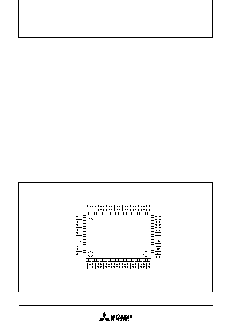
Fig. 1 M38224M6HXXXFP pin configuration
(The pin configuration of 80D0 is same as this.)
PIN CONFIGURATION (TOP VIEW)
Package type : 80P6N-A (80-pin plastic-molded QFP)
3822 Group
MITSUBISHI MICROCOMPUTERS
SINGLE-CHIP 8-BIT CMOS MICROCOMPUTER
S
E
G
8
S
E
G
9
P
3
4
/
S
E
G
1
2
P
3
5
/
S
E
G
1
3
P
0
0
/
S
E
G
1
6
P
0
3
/
S
E
G
1
9
P
0
4
/
S
E
G
2
0
P
0
5
/
S
E
G
2
1
P
0
6
/
S
E
G
2
2
P
0
7
/
S
E
G
2
3
P
1
1
/
S
E
G
2
5
P
1
2
/
S
E
G
2
6
P
1
3
/
S
E
G
2
7
P
1
4
/
S
E
G
2
8
P
1
5
/
S
E
G
2
9
P
1
6
/
S
E
G
3
0
P
1
7
/
S
E
G
3
1
V
L
1
P
6
7
/
A
N
7
M
3
8
2
2
4
M
6
H
X
X
X
F
P
P
5
7
/
A
D
T
P
5
0
/
I
N
T
2
P
4
6
/
S
C
L
K
P
4
5
/
T
X
D
P
4
3
/
I
N
T
1
P
4
2
/
I
N
T
0
A
V
S
S
V
R
E
F
V
C
C
S
E
G
0
P4
1
/
P
4
0
X
IN
X
OUT
V
SS
P2
7
P2
6
P2
5
P2
4
P2
3
P2
2
P2
1
P2
0
RESET
P
5
1
/
I
N
T
3
P
5
5
/
C
N
T
R
1
P
5
4
/
C
N
T
R
0
P
5
3
/
R
T
P
1
P
5
2
/
R
T
P
0
P
5
6
/
T
O
U
T
P
1
0
/
S
E
G
2
4
P
0
1
/
S
E
G
1
7
P
0
2
/
S
E
G
1
8
P
4
7
/
S
R
D
Y
S
E
G
1
0
S
E
G
1
1
P
3
6
/
S
E
G
1
4
P
3
7
/
S
E
G
1
5
P
7
0
/
X
C
O
U
T
P7
1
/X
CIN
COM
0
V
L
3
P
6
6
/
A
N
6
P
6
5
/
A
N
5
P
6
4
/
A
N
4
P
6
3
/
A
N
3
P
6
2
/
A
N
2
P
6
1
/
A
N
1
P
6
0
/
A
N
0
V
L
2
C
O
M
1
COM
2
C
O
M
3
S
E
G
1
S
E
G
2
S
E
G
3
S
E
G
4
S
E
G
5
S
E
G
6
S
E
G
7
P
4
4
/
R
X
D
1
2
3 4
5
6
7
8
9 1
0 1
1 12 1
3 1
4 1
5 1
6 1
7 1
8 1
9 20 2
1 22 2
3 24
2
5
2
6
2
7
2
8
2
9
3
0
3
1
3
2
3
3
3
4
3
5
3
6
3
7
3
8
3
9
4
0
41
4
2
43
4
4
45
4
6
47
4
8
49
5
0
51
52
53
5
4
55
56
57
5
8
5
9
6
0
61
6
2
6
3
6
4
6
5
6
6
6
7
6
8
6
9
7
0
7
1
7
2
7
3
7
4
7
5
76
7
7
78
7
9
8
0
2
SINGLE-CHIP 8-BIT CMOS MICROCOMPUTER
3822 Group
MITSUBISHI MICROCOMPUTERS
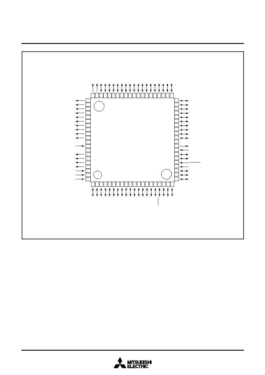
Package type : 80P6S-A/80P6Q-A
(80-pin plastic-molded QFP)
PIN CONFIGURATION (TOP VIEW)
Fig. 2 M38223M4MXXXGP/M38224M6HXXXHP pin configuration
1
2
3
4
7
8
9
1
0
1
1
1
2
1
3
1
4
1
5
1
6
1
7
1
8
1
9
2
0
5
6
2
1
2
2
2
3
24
25
2
6
2
7
2
8
29
30
31
3
2
3
3
3
4
35
3
6
37
3
8
3
9
4
0
4
1
4
2
4
3
4
4
4
5
4
6
4
7
4
8
4
9
5
0
5
1
5
2
5
3
5
4
5
5
5
6
5
7
5
8
5
9
6
0
61
62
63
64
65
66
67
68
69
70
71
72
73
74
75
76
77
78
79
80
P
1
4
/
S
E
G
2
8
P
1
5
/
S
E
G
2
9
P1
6
/SEG
30
P1
7
/SEG
31
P4
2
/INT
0
V
CC
X
IN
X
OUT
V
SS
P2
7
P2
6
P2
5
P2
4
P2
3
P2
2
P2
1
P2
0
RESET
P7
0
/X
COUT
P7
1
/X
CIN
P4
1
/
P4
0
P4
3
/INT
1
S
E
G
1
0
P
3
5
/
S
E
G
1
3
P
3
6
/
S
E
G
1
4
P
3
7
/
S
E
G
1
5
P
0
0
/
S
E
G
1
6
P
0
3
/
S
E
G
1
9
P
0
4
/
S
E
G
2
0
P
0
5
/
S
E
G
2
1
P
0
6
/
S
E
G
2
2
P
0
7
/
S
E
G
2
3
P
1
1
/
S
E
G
2
5
P
1
2
/
S
E
G
2
6
P
1
0
/
S
E
G
2
4
P
0
1
/
S
E
G
1
7
P
0
2
/
S
E
G
1
8
P
1
3
/
S
E
G
2
7
C
O
M
3
P
6
0
/
A
N
0
P
5
7
/
A
D
T
P
5
6
/
T
O
U
T
P
5
4
/
C
N
T
R
0
P
5
3
/
R
T
P
1
P
5
2
/
R
T
P
0
P
5
1
/
I
N
T
3
P
5
5
/
C
N
T
R
1
P
4
6
/
S
C
L
K
P
4
5
/
T
X
D
P
5
0
/
I
N
T
2
P
4
7
/
S
R
D
Y
P
4
4
/
R
X
D
SEG
1
SEG
2
S
E
G
3
S
E
G
4
S
E
G
6
S
E
G
5
S
E
G
7
SEG
0
S
E
G
8
SEG
9
COM
2
COM
1
COM
0
V
L3
V
L
2
V
L1
V
R
E
F
A
V
S
S
P
6
1
/
A
N
1
P
6
2
/
A
N
2
P
6
3
/
A
N
3
P
6
4
/
A
N
4
P
6
5
/
A
N
5
P
6
6
/
A
N
6
P
6
7
/
A
N
7
S
E
G
1
1
P
3
4
/
S
E
G
1
2
M38223M4MXXXGP
M38224M6HXXXHP
3
SINGLE-CHIP 8-BIT CMOS MICROCOMPUTER
3822 Group
MITSUBISHI MICROCOMPUTERS
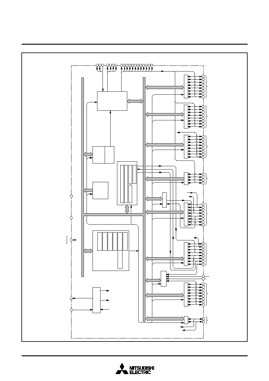
FUNCTIONAL BLOCK DIAGRAM (Package type : 80P6Q-A)
Fig. 3 Functional block diagram
K
e
y
o
n
w
a
k
e
u
p
R
e
a
l
t
i
m
e
p
o
r
t
f
u
n
c
t
i
o
n
I
N
T
2
,
I
N
T
3
C
N
T
R
0
,
C
N
T
R
1
T
O
U
T
A
D
T
I
N
T
0
,
I
N
T
1
R
T
P
0
,
R
T
P
1
D
a
t
a
b
u
s
C
P
U
A
X
Y
S
P
C
H
P
C
L
P
S
R
E
S
E
TV
C
C
V
S
S
R
e
s
e
t
I
n
p
u
t(
5
V
)
(
0
V
)
R
O
M
R
A
M
L
C
D
d
i
s
p
l
a
y
R
A
M
(
1
6
b
y
t
e
s
)
2
5
7
13
0
I
/
O
P
o
r
t
P
5
P
4
(
8
)
I
/
O
P
o
r
t
P
4
I
/
O
P
o
r
t
P
2
P
2
(
8
)
I
/
O
P
o
r
t
P
0
P
0
(
8
)
I
/
O
P
o
r
t
P
1
P
1
(
8
)
P
6
(
8
)
I
n
p
u
t
P
o
r
t
P
3
P
3
(
4
)
I
/
O
P
o
r
t
P
6
P
5
(
8
)
I
/
O
P
o
r
t
P
7
P
7
(
2
)
8
0
7
9
7
8
7
7
7
6
7
5
7
4
7
0
6
9
6
8
6
7
6
6
6
5
6
4
6
3
6
2
6
1
6
0
5
9
4
7
4
8
4
9
5
0
5
1
5
25
35
4
3
94
04
14
24
34
44
54
6
3
13
23
33
43
53
63
73
8
5
55
65
75
8
1
92
02
12
22
32
4
1
71
8
2
62
7
123
456
78
7
3
7
2
1
01
11
21
31
41
51
6
9
C
l
o
c
k
g
e
n
e
r
a
t
i
n
g
c
i
r
c
u
i
t
M
a
i
n
C
l
o
c
k
I
n
p
u
t
X
I
N
M
a
i
n
C
l
o
c
k
O
u
t
p
u
t
X
O
U
T
X
C
O
U
T
S
u
b
-
C
l
o
c
k
O
u
t
p
u
t
X
C
I
N
S
u
b
-
C
l
o
c
k
I
n
p
u
t
S
I
/
O
(
8
)
V
R
E
F
A
V
S
S
(
0
V
)
A
-
D
c
o
n
v
e
r
t
e
r
(
8
)
T
i
m
e
r
X
(
1
6
)
T
i
m
e
r
Y
(
1
6
)
T
i
m
e
r
1
(
8
)T
i
m
e
r
2
(
8
)
T
i
m
e
r
3
(
8
)
L
C
D
d
r
i
v
e
c
o
n
t
r
o
l
c
i
r
c
u
i
t
V
L
1
V
L
2
V
L
3
C
O
M
0
C
O
M
1
C
O
M
2
C
O
M
3
S
E
G
0
S
E
G
1
S
E
G
2
S
E
G
3
S
E
G
4
S
E
G
5
S
E
G
6
S
E
G
7
S
E
G
8
S
E
G
9
S
E
G
1
0
S
E
G
1
1
X
C
I
N
X
C
O
U
T
2
8
2
9
4
SINGLE-CHIP 8-BIT CMOS MICROCOMPUTER
3822 Group
MITSUBISHI MICROCOMPUTERS
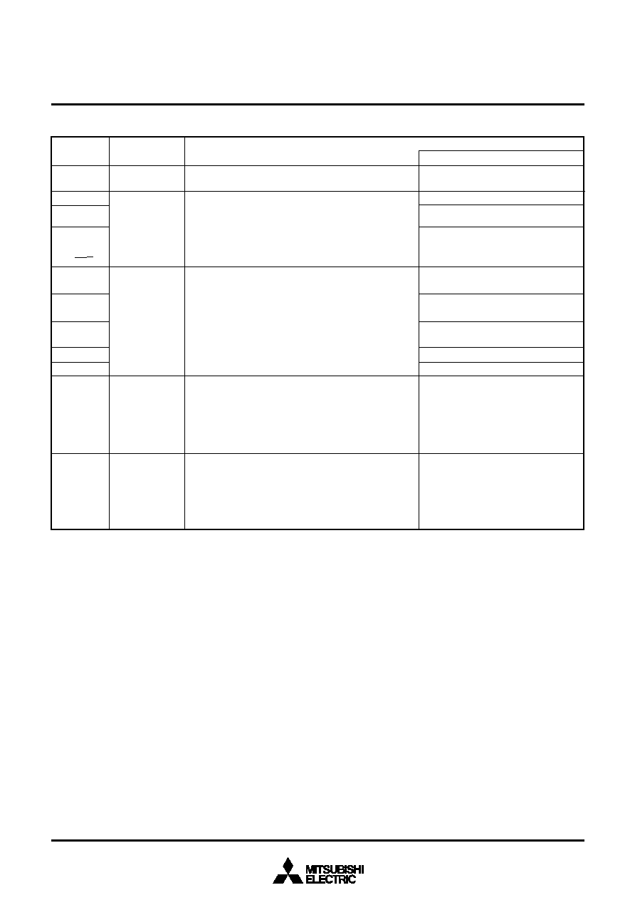
PIN DESCRIPTION
Table 1 Pin description (1)
V
CC
, V
SS
Function
Pin
Name
Function except a port function
∑LCD segment output pins
Power source
∑Apply voltage of power source to V
CC
, and 0 V to V
SS
. (For the limits of V
CC
, refer to "Recom-
mended operating conditions").
V
REF
AV
SS
RESET
X
IN
X
OUT
V
L1
≠V
L3
COM
0
≠COM
3
SEG
0
≠SEG
11
P0
0
/SEG
16
≠
P0
7
/SEG
23
P1
0
/SEG
24
≠
P1
7
/SEG
31
P2
0
≠ P2
7
P3
4
/SEG
12
≠
P3
7
/SEG
15
Analog refer-
ence voltage
Analog power
source
Reset input
Clock input
Clock output
LCD power
source
Common output
Segment output
I/O port P0
I/O port P1
I/O port P2
∑Reference voltage input pin for A-D converter.
∑GND input pin for A-D converter.
∑Connect to V
SS
.
∑Reset input pin for active "L".
∑Input and output pins for the main clock generating circuit.
∑Feedback resistor is built in between X
IN
pin and X
OUT
pin.
∑Connect a ceramic resonator or a quartz-crystal oscillator between the X
IN
and X
OUT
pins to set
the oscillation frequency.
∑If an external clock is used, connect the clock source to the X
IN
pin and leave the X
OUT
pin open.
∑This clock is used as the oscillating source of system clock.
∑Input 0
V
L1
V
L2
V
L3
V
CC
voltage.
∑Input 0 ≠ V
L3
voltage to LCD.
∑LCD common output pins.
∑COM
2
and COM
3
are not used at 1/2 duty ratio.
∑COM
3
is not used at 1/3 duty ratio.
∑LCD segment output pins.
∑8-bit output port.
∑CMOS compatible input level.
∑CMOS 3-state output structure.
∑I/O direction register allows each port to be individually
programmed as either input or output.
∑Pull-down control is enabled.
∑8-bit I/O port.
∑CMOS compatible input level.
∑CMOS 3-state output structure.
∑I/O direction register allows each pin to be individually
programmed as either input or output.
∑Pull-up control is enabled.
∑4-bit input port.
∑CMOS compatible input level.
∑Pull-down control is enabled.
∑Key input (key-on wake-up) interrupt
input pins
∑LCD segment output pins
Input port P3
5
SINGLE-CHIP 8-BIT CMOS MICROCOMPUTER
3822 Group
MITSUBISHI MICROCOMPUTERS
Table 2 Pin description (2)
Function
Pin
Name
Function except a port function
P4
0
P4
2
/INT
0
,
P4
3
/INT
1
P4
4
/R
X
D,
P4
5
/T
X
D,
P4
6
/S
CLK
,
P4
7
/S
RDY
P5
0
/INT
2
,
P5
1
/INT
3
P5
2
/RTP
0
,
P5
3
/RTP
1
P5
4
/CNTR
0
,
P5
5
/CNTR
1
P5
6
/T
OUT
P5
7
/ADT
P6
0
/AN
0
≠
P6
7
/AN
7
P7
0
/X
COUT,
P7
1
/X
CIN
I/O port P4
I/O port P5
I/O port P6
I/O port P7
∑1-bit Input port.
∑CMOS compatible input level.
∑7-bit I/O port.
∑CMOS compatible input level.
∑CMOS 3-state output structure.
∑I/O direction register allows each pin to be individually
programmed as either input or output.
∑Pull-up control is enabled.
∑8-bit I/O port.
∑CMOS compatible input level.
∑CMOS 3-state output structure.
∑I/O direction register allows each pin to be individually
programmed as either input or output.
∑Pull-up control is enabled.
∑8-bit I/O port.
∑CMOS compatible input level.
∑CMOS 3-state output structure.
∑I/O direction register allows each pin to be individually
programmed as either input or output.
∑Pull-up control is enabled.
∑2-bit I/O port.
∑CMOS compatible input level.
∑CMOS 3-state output structure.
∑I/O direction register allows each pin to be individually
programmed as either input or output.
∑Pull-up control is enabled.
∑
clock output pin
∑Interrupt input pins
∑Interrupt input pins
∑Real time port function pins
∑Timer X, Y function pins
∑Timer 2 output pins
∑A-D conversion input pins
∑Sub-clock generating circuit I/O pins.
(Connect a resonator. External clock
cannot be used.)
Input port P4
P4
1
/
∑Serial I/O function pins
∑A-D trigger input pins