DESCRIPTION
The 3825 group is the 8-bit microcomputer based on the 740 fam-
ily core technology.
The 3825 group has the LCD drive control circuit, an 8-channel A-
D converter, and a Serial I/O as additional functions.
The various microcomputers in the 3825 group include variations
of internal memory size and packaging. For details, refer to the
section on part numbering.
For details on availability of microcomputers in the 3825 group, re-
fer the section on group expansion.
FEATURES
∑
Basic machine-language instructions ....................................... 71
∑
The minimum instruction execution time ............................ 0.5 µs
(at 8MHz oscillation frequency)
∑
Memory size
ROM .................................................................. 4 K to 60 K bytes
RAM ................................................................. 192 to 2048 bytes
∑
Programmable input/output ports ............................................. 43
∑
Software pull-up/pull-down resistors (Ports P0≠P8)
∑
Interrupts .................................................. 17 sources, 16 vectors
(includes key input interrupt)
∑
Timers ........................................................... 8-bit
!
3, 16-bit
!
2
∑
Serial I/O ...................... 8-bit
!
1 (UART or Clock-synchronized)
∑
A-D converter .................................................. 8-bit
!
8 channels
∑
LCD drive control circuit
Bias ................................................................................... 1/2, 1/3
Duty ............................................................................ 1/2, 1/3, 1/4
Common output .......................................................................... 4
Segment output ......................................................................... 40
∑
2 Clock generating circuits
Clock (X
IN
-X
OUT
) .................................. Internal feedback resistor
Sub-clock (X
CIN
-X
COUT
) .......... Without internal feedback resistor
(connect to external ceramic resonator or quartz-crystal oscillator)
∑
Power source voltage
In high-speed mode ................................................... 4.0 to 5.5 V
In middle-speed mode ............................................... 2.5 to 5.5 V
(Low power source version: 2.2 V to 5.5 V)
(Extended operating temperature version: 3.0 V to 5.5 V)
In low-speed mode ..................................................... 2.5 to 5.5 V
(Low power source version: 2.2 V to 5.5 V)
(Extended operating temperature version: 3.0 V to 5.5 V)
∑
Power dissipation
In high-speed mode ........................................................... 32 mW
(at 8 MHz oscillation frequency, at 5 V power source voltage)
In low-speed mode .............................................................. 45 µW
(at 32 kHz oscillation frequency, at 3 V power source voltage)
∑
Operating temperature range ................................... ≠ 20 to 85∞C
(Extended operating temperature version: ≠40 to 85∞C)
APPLICATIONS
Camera, household appliances, consumer electronics, etc.
3825 Group
MITSUBISHI MICROCOMPUTERS
SINGLE-CHIP 8-BIT CMOS MICROCOMPUTER
M38258MCMXXXFP
1
2
3
4
5
6
7
8
9
10
11
12
13
14
15
16
17
18
19
20
21
22
23
24
25
26
27
28
29
30
P5
0
/INT
2
P4
7
/S
RDY
C
1
V
L1
P5
7
/ADT
P4
6
/S
CLK
P4
4
/R
X
D
P4
3
/INT
1
P4
2
/INT
0
P5
4
/CNTR
0
P5
2
/RTP
0
P5
3
/RTP
1
P5
1
/INT
3
P5
5
/CNTR
1
P6
7
/AN
7
P6
6
/AN
6
P6
5
/AN
5
P6
4
/AN
4
P6
3
/AN
3
P6
2
/AN
2
P6
1
/AN
1
P6
0
/AN
0
P5
6
/
T
OUT
P4
5
/
T
X
D
P4
1
/ f(X
IN
)/5 / f(X
IN
)/10
P4
0
/ f(X
IN
) / f(X
IN
)/2
P7
7
P7
6
P7
5
P7
4
31
32
33
34
35
36
37
38
39
40
41
42
49
50
43
44
45
46
47
48
P7
0
X
IN
X
OUT
V
SS
P2
7
P2
6
P2
5
P2
4
P2
3
P2
2
P2
1
P2
0
RESET
P8
0
/X
COUT
P8
1
/X
CIN
P1
7
P1
6
P7
1
P7
2
P7
3
80
79
78
77
76
75
74
73
72
71
70
69
68
67
66
65
64
63
62
61
59
58
57
60
56
54
53
52
55
51
SEG
10
SEG
11
SEG
12
SEG
13
SEG
14
SEG
15
SEG
16
SEG
17
P3
0
/SEG
18
P3
1
/SEG
19
P3
2
/SEG
20
P3
3
/SEG
21
P3
4
/SEG
22
P3
5
/SEG
23
P3
6
/SEG
24
P3
7
/SEG
25
P0
1
/SEG
27
P0
2
/SEG
28
P0
3
/SEG
29
P0
4
/SEG
30
P0
5
/SEG
31
P0
6
/SEG
32
P0
7
/SEG
33
P1
2
/SEG
36
P1
3
/SEG
37
P1
4
/SEG
38
P1
5
/SEG
39
P0
0
/SEG
26
P1
0
/SEG
34
P1
1
/SEG
35
99
98
97
96
95
94
93
92
91
90
89
88
87
86
85
84
83
82
81
V
CC
SEG
6
SEG
7
SEG
5
SEG
3
SEG
4
SEG
2
SEG
1
SEG
0
V
REF
AV
SS
COM
2
COM
3
COM
1
COM
0
V
L3
SEG
8
SEG
9
V
L2
C
2
100
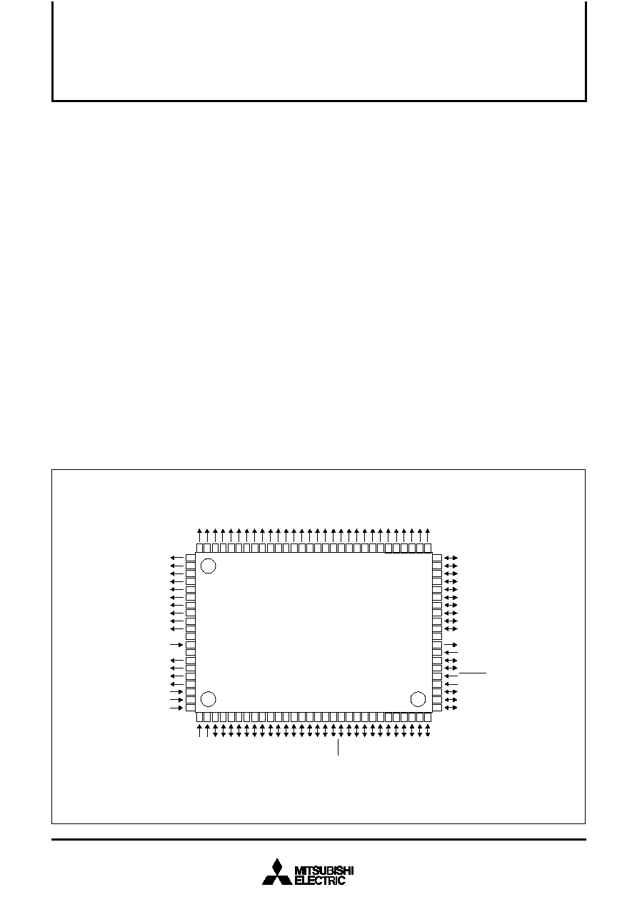
Package type : 100P6S-A (100-pin plastic-molded QFP)
Fig. 1 Pin configuration of M38258MCMXXXFP
PIN CONFIGURATION (TOP VIEW)

SINGLE-CHIP 8-BIT CMOS MICROCOMPUTER
MITSUBISHI MICROCOMPUTERS
3825 Group
4
PIN DESCRIPTION
Table 1. Pin description (1)
Function
∑ Apply voltage of 2.2 V to 5.5 V to V
CC
, and 0 V to V
SS
.
∑ Reference voltage input pin for A-D converter.
∑ GND input pin for A-D converter.
∑ Connect to V
SS
.
∑ Reset input pin for active "L"
∑ Input and output pins for the main clock generating circuit.
∑ Feedback resistor is built in between X
IN
pin and X
OUT
pin.
∑ Connect a ceramic resonator or a quartz-crystal oscillator between the X
IN
and X
OUT
pins to set
the oscillation frequency.
∑ If an external clock is used, connect the clock source to the X
IN
pin and leave the X
OUT
pin open.
∑ This clock is used as the oscillating source of system clock.
∑ Input 0
V
L1
V
L2
V
L3
V
CC
voltage
∑ Input 0 ≠ V
L3
voltage to LCD
∑ External capacitor pins for a voltage multiplier (3 times) of LCD contorl.
∑ LCD common output pins
∑ COM
2
and COM
3
are not used at 1/2 duty ratio.
∑ COM
3
is not used at 1/3 duty ratio.
∑ LCD segment output pins
∑ 8-bit output port
∑ CMOS 3-state output structure
∑ Pull-down control is enabled.
∑ Port output control is enabled.
∑ 6-bit output port
∑ CMOS 3-state output structure
∑ Pull-down control is enabled.
∑ Port output control is enabled.
∑ 2-bit I/O port
∑ CMOS compatible input level
∑ CMOS 3-state output structure
∑ I/O direction register allows each pin to be individually programmed as either input or output.
∑ Pull-up control is enabled.
∑ 8-bit Input port
∑ CMOS compatible input level
∑ CMOS 3-state output structure
∑ I/O direction register allows each pin to be individually
programmed as either input or output.
∑ Pull-up control is enabled.
∑ 8-bit output port
∑ CMOS 3-state output structure
∑ Pull-down control is enabled.
∑ Port output control is enabled.
∑ LCD segment pins
∑ Key input (key-on wake up) interrupt
input pins
∑ LCD segment pins
Pin
V
CC
, V
SS
V
REF
AV
SS
RESET
X
IN
X
OUT
V
L1
≠ V
L3
C
1
, C
2
COM
0
≠ COM
3
SEG
0
≠ SEG
17
P0
0
/SEG
26
≠
P0
7
/SEG
33
P1
0
/SEG
34
≠
P1
5
/SEG
39
P1
6
, P1
7
P2
0
≠ P2
7
P3
0
/SEG
18
≠
P3
7
/SEG
25
Name
Power source
Analog reference
voltage
Analog power
source
Reset input
Clock input
Clock output
LCD power source
Charge-pump
capacitor pin
Common output
Segment output
Output port P0
Output port P1
I/O port P1
I/O port P2
Output port P3
Function except a port function

SINGLE-CHIP 8-BIT CMOS MICROCOMPUTER
MITSUBISHI MICROCOMPUTERS
3825 Group
5
Function
∑ 8-bit I/O port
∑ CMOS compatible input level
∑ CMOS 3-state output structure
∑ I/O direction register allows each pin to be individually
programmed as either input or output.
∑ Pull-up control is enabled.
∑ 8-bit I/O port
∑ CMOS compatible input level
∑ CMOS 3-state output structure
∑ I/O direction register allows each pin to be individually
programmed as either input or output.
∑ Pull-up control is enabled.
∑ 8-bit I/O port
∑ CMOS compatible input level
∑ CMOS 3-state output structure
∑ I/O direction register allows each pin to be individually
programmed as either input or output.
∑ Pull-up control is enabled.
∑ 1-bit input port
∑ CMOS compatible input level
∑ 7-bit I/O port
∑ CMOS compatible input level
∑ CMOS 3-state output structure
∑ I/O direction register allows each pin to be individually programmed as either input or output.
∑ Pull-up control is enabled.
∑ 2-bit I/O port
∑ CMOS compatible input level
∑ CMOS 3-state output structure
∑ I/O direction register allows each pin to be individually
programmed as either input or output.
∑ Pull-up control is enabled.
Pin
P4
0
/f(X
IN
)/
f(X
IN
)/2,
P4
1
/f(X
IN
)/5/
f(X
IN
)/10
P4
2
/INT
0
,
P4
3
/INT
1
P4
4
/R
X
D,
P4
5
/T
X
D,
P4
6
/S
CLK
,
P4
7
/S
RDY
P5
0
/INT
2
,
P5
1
/INT
3
P5
2
/RTP
0
,
P5
3
/RTP
1
P5
4
/CNTR
0
,
P5
5
/CNTR
1
P5
6
/T
OUT
P5
7
/ADT
P6
0
/AN
0≠
P6
7
/AN
7
P7
0
P7
1
≠P7
7
P8
0
/X
COUT
,
P8
1
/X
CIN
Name
I/O port P4
I/O port P5
I/O port P6
Input port P7
I/O port P7
I/O port P8
Function except a port function
∑ Clock output pins
∑ Interrupt input pins
∑ Serial I/O function pins
∑ Interrupt input pins
∑ Real time port function pins
∑ Timers X, Y functions pins
∑ Timer 2 output pin
∑ A-D trigger input pin
∑ A-D conversion input pins
Table 2. Pin description (2)
∑Sub-clock generating circuit I/O pins
(Connect a resonator. External clock
cannot be used.)

