Äîêóìåíòàöèÿ è îïèñàíèÿ www.docs.chipfind.ru
1
2
3
4
5
6
7
8
9
10
11
12
13
14
15
16
17
18
19
20
21
22
23
24
25
26
27
28
29
30
31
32
33
34
35
36
37
38
39
40
41
42
43
44
45
46
47
48
49
50
51
52
53
54
55
56
57
58
59
60
61
62
63
64
65
66
67
68
69
70
71
72
73
74
75
76
77
78
79
80
81
82
83
84
85
86
87
88
89
90
91
92
93
94
95
96
97
98
99
100
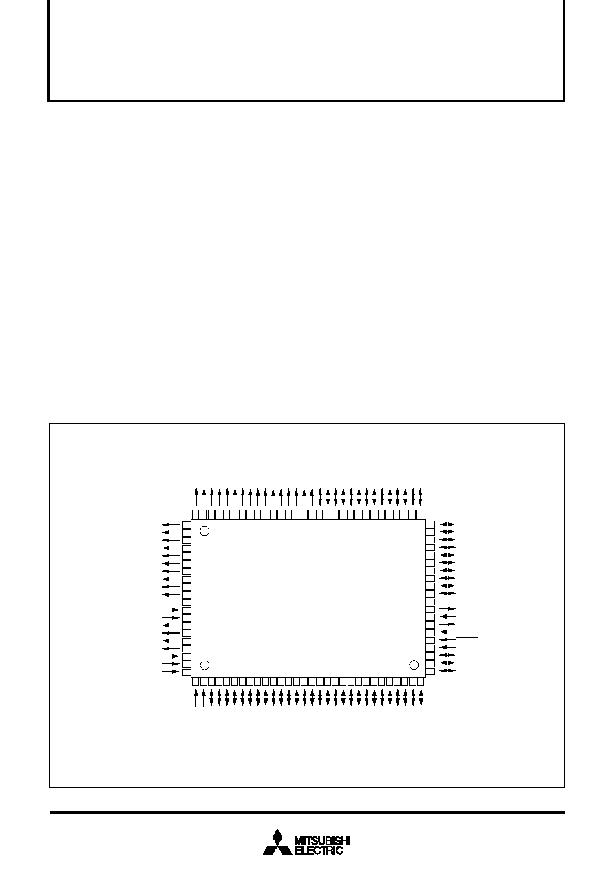
M38277M8MXXXFP
SEG
9
P3
1
/SEG
19
P3
0
/SEG
18
P3
2
/SEG
20
P3
3
/SEG
21
P3
4
/SEG
22
SEG
10
SEG
11
SEG
12
SEG
13
SEG
14
SEG
15
P3
5
/SEG
23
P3
6
/SEG
24
P3
7
/SEG
25
P0
0
/SEG
26
P0
1
/SEG
27
P0
2
/SEG
28
P0
3
/SEG
29
P0
4
/SEG
30
P0
5
/SEG
31
P0
6
/SEG
32
P0
7
/SEG
33
P1
0
/SEG
34
P1
1
/SEG
35
P1
2
/SEG
36
P1
3
/SEG
37
P1
4
/SEG
38
P1
5
/SEG
39
C
1
V
L1
P6
7
/AN
7
P6
6
/AN
6
P6
5
/AN
5
P6
4
/AN
4
P6
2
/S
CLK21
/AN
2
P6
1
/S
OUT2
/AN
1
P6
0
/S
IN2
/AN
0
P5
7
/DA
2
P5
6
/DA
1
P5
5
/CNTR
1
P5
4
/CNTR
0
P5
3
/RTP
1
P5
2
/RTP
0
P5
1
/PWM
1
P5
0
/PWM
0
P4
6
/S
CLK1
P4
5
/T
X
D
P4
4
/R
X
D
P4
3
/
/T
OUT
P4
2
/INT
2
P4
1
/INT
1
P4
0
/ADT
P7
7
P7
6
P7
5
P7
4
C
2
V
L2
V
L3
COM
0
COM
1
COM
2
V
REF
AV
SS
V
CC
SEG
8
SEG
0
SEG
1
SEG
2
SEG
4
SEG
5
SEG
6
SEG
7
SEG
3
P7
2
P7
3
P7
1
P7
0
/INT
0
X
CIN
X
COUT
X
IN
X
OUT
V
SS
P2
7
P2
6
P2
5
P2
4
P2
3
P2
1
P1
6
P2
2
P2
0
P1
7
RESET
SEG
16
SEG
17
COM
3
P4
7
/S
RDY1
P6
3
/S
CLK22
/AN
3
DESCRIPTION
The 3827 group is the 8-bit microcomputer based on the 740 fam-
ily core technology.
The 3827 group has the LCD drive control circuit, the A-D/D-A
converter, the UART, and the PWM as additional functions.
The various microcomputers in the 3827 group include variations
of internal memory size and packaging. For details, refer to the
section on part numbering.
For details on availability of microcomputers in the 3827 group, re-
fer to the section on group expansion.
FEATURES
q
Basic machine-language instructions ...................................... 71
q
The minimum instruction execution time ........................... 0.5
µ
s
(at 8MHz oscillation frequency)
q
Memory size
ROM ................................................................. 4 K to 60 K bytes
RAM ................................................................. 192 to 2048 bytes
q
Programmable input/output ports ............................................ 55
q
Output port ................................................................................. 8
q
Input por t .................................................................................... 1
q
Interrupts ................................................. 17 sources, 16 vectors
(includes key input interrupt)
q
Timers ........................................................... 8-bit
!
3, 16-bit
!
2
q
Serial I/O1 .................... 8-bit
!
1 (UART or Clock-synchronized)
q
Serial I/O2 ...................................8-bit
!
1 (Clock-synchronized)
q
PWM output .................................................................... 8-bit
!
1
q
A-D converter ............................................... 10-bit
!
8 channels
q
D-A converter ................................................. 8-bit
!
2 channels
q
LCD drive control circuit
Bias ................................................................................... 1/2, 1/3
Duty ........................................................................... 1/2, 1/3, 1/4
Common output .......................................................................... 4
Segment output ........................................................................ 40
q
2 Clock generating circuits
(connect to external ceramic resonator or quartz-crystal oscillator)
q
Watchdog timer ............................................................ 14-bit
!
1
q
Power source voltage ................................................ 2.2 to 5.5 V
q
Power dissipation
In high-speed mode .......................................................... 40 mW
(at 8 MHz oscillation frequency, at 5 V power source voltage)
In low-speed mode ............................................................ 60
µ
W
(at 32 kHz oscillation frequency, at 3 V power source voltage)
q
Operating temperature range ................................... 20 to 85
°
C
APPLICATIONS
Camera, wireless phone, etc.
3827 Group
MITSUBISHI MICROCOMPUTERS
SINGLE-CHIP 8-BIT CMOS MICROCOMPUTER
Fig. 1 M38277M8MXXXFP pin configuration
PIN CONFIGURATION (TOP VIEW)
Package type : 100P6S-A (100-pin plastic-molded QFP)
2
SINGLE-CHIP 8-BIT CMOS MICROCOMPUTER
3827 Group
MITSUBISHI MICROCOMPUTERS
M38277M8MXXXGP
M38277M8MXXXHP
1
2
3
4
5
6
7
8
9
10
11
12
13
14
15
16
17
18
19
20
21
22
23
24
25
P5
0
/PWM
0
P4
7
/S
RDY1
P5
7
/DA
2
P4
6
/S
CLK1
P4
4
/R
X
D
P4
3
/
/T
OUT
P4
2
/INT
2
P5
4
/CNTR
0
P5
2
/RTP
0
P5
3
/RTP
1
P5
1
/PWM
1
P5
5
/CNTR
1
P6
7
/AN
7
P6
6
/AN
6
P6
5
/AN
5
P6
4
/AN
4
P6
3
/S
CLK22
/AN
3
P6
2
/S
CLK21
/AN
2
P6
1
/S
OUT2
/AN
1
P6
0
/S
IN2
/AN
0
P4
5
/
T
X
D
P4
1
/INT
1
P4
0
/ADT
P7
7
31
32
33
34
35
36
37
38
39
40
41
42
49
50
43
44
45
46
47
48
75
74
73
72
71
70
69
68
67
66
65
64
63
62
61
59
58
57
60
56
54
53
52
55
51
SEG
13
SEG
14
SEG
15
SEG
16
SEG
17
P3
0
/SEG
18
P3
1
/SEG
19
P3
2
/SEG
20
P3
3
/SEG
21
P3
4
/SEG
22
P3
5
/SEG
23
P3
6
/SEG
24
P3
7
/SEG
25
P0
1
/SEG
27
P0
2
/SEG
28
P0
3
/SEG
29
P0
4
/SEG
30
P0
5
/SEG
31
P0
6
/SEG
32
P0
7
/SEG
33
P1
2
/SEG
36
P1
3
/SEG
37
P0
0
/SEG
26
P1
0
/SEG
34
P1
1
/SEG
35
99
98
97
96
95
94
93
92
91
90
89
88
87
86
85
84
83
82
81
100
26
27
28
29
30
P7
0
/INT
0
X
IN
X
OUT
V
SS
P2
7
P2
6
P2
5
P2
4
P2
3
P2
2
P2
1
P2
0
RESET
X
COUT
X
CIN
P1
7
P1
6
P7
1
P7
2
P7
3
P7
4
P7
5
P7
6
P1
5
/SEG
39
P1
4
/SEG
38
76
77
78
79
80
V
CC
SEG
6
SEG
7
SEG
5
SEG
3
SEG
4
SEG
2
SEG
1
SEG
0
V
REF
AV
SS
COM
2
COM
3
COM
1
COM
0
V
L3
SEG
8
SEG
9
V
L2
C
2
C
1
V
L1
SEG
10
SEG
11
SEG
12
P5
6
/DA
1
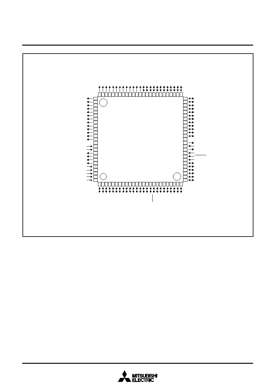
Package type : GP........ 100P6Q-A (100-pin plastic-molded LQFP)
Package type : HP ........ 100PFB-A (100-pin plastic-molded TQFP)
PIN CONFIGURATION (TOP VIEW)
Fig. 2 M38277M8MXXXGP/M38277M8MXXXHP pin configuration
3
SINGLE-CHIP 8-BIT CMOS MICROCOMPUTER
MITSUBISHI MICROCOMPUTERS
3827 Group
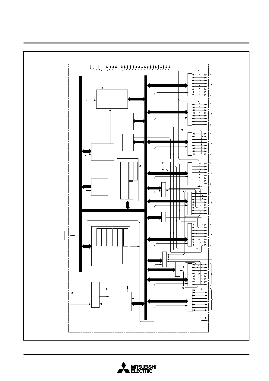
FUNCTIONAL BLOCK DIA
GRAM
Fig. 3 Functional block diagram
Key input/key-on wake-up interrupt
INT
1,
INT
2
CNTR
0
,CNTR
1
DA
1
DA
2
T
OUT
INT
0
ADT
Data bus
C P U
A
X
Y
S
PC
H
PC
L
PS
RESET
V
CC
V
SS
Reset input
( 5 V )
( 0 V )
R O M
R A M
LCD display
RAM
(20 bytes)
I/O port P5
P4(8)
I/O port P4
I/O port P2
P2(8)
I/O port P0
P0(8)
I/O port P1
P1(8)
P6(8)
I/O port P7
P7(8)
Output port P3
P3(8)
I/O port P6
P5(8)
Sub-clock input
Sub-clock output
X
CIN
X
COUT
Clock generating circuit
X
IN
OUT
X
Main clock input
Main clock output
COUT
X
X
CIN
Sub-clock output
Sub-clock input
SI/O1 (8)
V
REF
AV
SS
A-D converter
(10)
Timer X(16)
Timer Y(16)
Timer 1(8)
Timer 2(8)
Timer 3(8)
LCD drive
control circuit
V
L1
C
1
C
2
V
L2
V
L3
COM
0
COM
1
COM
2
COM
3
SEG
0
SEG
1
SEG
2
SEG
3
SEG
4
SEG
5
SEG
6
SEG
7
SEG
8
SEG
9
SEG
10
SEG
11
SEG
12
SEG
13
SEG
14
SEG
15
SEG
16
SEG
17
X
CIN
COUT
X
SI/O2(8)
Watchdog timer
Reset
PWM(8)
Real time port function
D-A2
D-A1
4
SINGLE-CHIP 8-BIT CMOS MICROCOMPUTER
3827 Group
MITSUBISHI MICROCOMPUTERS
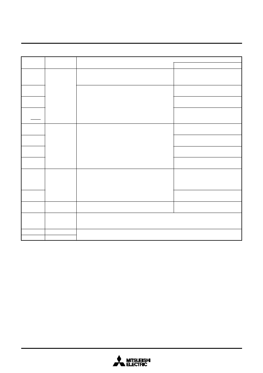
PIN DESCRIPTION
Table 1 Pin description (1)
V
CC
, V
SS
Function
Pin
Name
Function except a port function
·LCD segment output pins
Power source
·Apply voltage of 2.2 V to 5.5 V to V
CC
, and 0 V to V
SS
.
V
REF
AV
SS
RESET
X
IN
X
OUT
V
L1
V
L3
C
1
, C
2
COM
0
COM
3
SEG
0
SEG
17
P0
0
/SEG
26
P0
7
/SEG
33
P1
0
/SEG
34
P1
5
/SEG
39
P1
6
, P1
7
P2
0
P2
7
P3
0
/SEG
18
P3
7
/SEG
25
Analog refer-
ence voltage
Analog power
source
Reset input
Clock input
Clock output
LCD power
source
Charge-pump
capacitor pin
Common output
Segment output
I/O port P0
I/O port P1
I/O port P2
Output port P3
·Reference voltage input pin for A-D converter and D-A converter.
·GND input pin for A-D converter and D-A converter.
·Connect to V
SS
.
·Reset input pin for active "L".
·Input and output pins for the main clock generating circuit.
·Connect a ceramic resonator or a quartz-crystal oscillator between the X
IN
and X
OUT
pins to set
the oscillation frequency.
·If an external clock is used, connect the clock source to the X
IN
pin and leave the X
OUT
pin open.
·Input 0
V
L1
V
L2
V
L3
V
CC
voltage.
·Input 0 V
L3
voltage to LCD.
·External capacitor pins for a voltage multiplier (3 times) of LCD contorl.
·LCD common output pins.
·COM
2
and COM
3
are not used at 1/2 duty ratio.
·COM
3
is not used at 1/3 duty ratio.
·LCD segment output pins.
·8-bit output port.
·CMOS compatible input level.
·CMOS 3-state output structure.
·Pull-up control is enabled.
·I/O direction register allows each port to be individually
programmed as either input or output.
·6-bit output port with same function as port P0.
·CMOS compatible input level.
·CMOS 3-state output structure.
·Pull-up control is enabled.
·I/O direction register allows each 6-bit pin to be pro-
grammed as either input or output.
·2-bit I/O port.
·CMOS compatible input level.
·CMOS 3-state output structure.
·I/O direction register allows each pin to be individually programmed as either input or output.
·Pull-up control is enabled.
·8-bit I/O port with same function as por t P0.
·CMOS compatible input level.
·CMOS 3-state output structure.
·Pull-up control is enabled.
·8-bit output port with same function as port P0.
·CMOS 3-state output structure.
·Port output control is enabled.
·Key input (key-on wake-up) interrupt
input pins
·LCD segment output pins
5
SINGLE-CHIP 8-BIT CMOS MICROCOMPUTER
MITSUBISHI MICROCOMPUTERS
3827 Group
Table 2 Pin description (2)
Function
Pin
Name
Function except a port function
·A-D trigger input pin
·Interrupt input pin
P4
0
/ADT
P4
1
/INT
1
,
P4
2
/INT
2
P4
3
/
/T
OUT
P4
4
/R
X
D,
P4
5
/T
X
D,
P4
6
/S
CLK1
,
P4
7
/S
RDY1
P5
0
/PWM
0
,
P5
1
/PWM
1
P5
2
/RTP
0
,
P5
3
/RTP
1
P5
4
/CNTR
0
,
P5
5
/CNTR
1
P5
6
/DA
1
,
P5
7
/DA
2
P6
0
/AN
0
/S
IN2,
P6
1
/AN
1
/S
OUT2,
P6
2
/AN
2
/S
CLK21,
P6
3
/AN
3
/S
CLK22
P6
4
/AN
4
P6
7
/AN
7
P7
0
/INT
0
P7
1
P7
7
X
COUT
X
CIN
I/O port P4
I/O port P5
I/O port P6
Input port P7
I/O port P7
Sub-clock output
Sub-clock input
·1-bit I/O port with same function as P1
6
and P1
7
.
·CMOS compatible input level.
·CMOS 3-state output structure.
·7-bit I/O port with same function as P1
6
and P1
7
.
·CMOS compatible input level.
·CMOS 3-state output structure.
·Pull-up control is enabled.
·8-bit I/O por t with same function as P1
6
and P1
7
.
·CMOS compatible input level.
·CMOS 3-state output structure.
·Pull-up control is enabled.
·8-bit I/O por t with same function as P1
6
and P1
7
.
·CMOS compatible input level.
·CMOS 3-state output structure.
·Pull-up control is enabled.
·1-bit I/O port.
·CMOS compatible input level.
·7-bit I/O port with same function as P1
6
and P1
7
.
·CMOS compatible input level.
·N-channel open-drain output structure.
·Sub-clock generating circuit I/O pins.
(Connect a resonator. External clock cannot be used.)
·Interrupt input pins
·
clock output pin
·Timer 2 output pin
·Serial I/O1 I/O pins
·PWM function pins
·Real time port function pins
·Timer X, Y function pins
·D-A conversion output pins
·A-D conversion input pins
·Serial I/O2 I/O pins
·A-D conversion input pins
·Interrupt input pin
Document Outline
- DESCRIPTION
- FEATURES
- APPLICATIONS
- PIN CONFIGURATION (TOP VIEW)
- M38277M8MXXXFP
- M38277M8MXXXGP, M38277M8MXXXHP
-
FUNCTIONAL BLOCK DIAGRAM
- PIN DESCRIPTION
- PART NUMBERING
- GROUP EXPANSION
- Memory Type
- Memory Size
- Package
- FUNCTIONAL DESCRIPTION
- Central Processing Unit (CPU)
- [CPU Mode Register (CPUM)]
- MEMORY
- Special Function Register (SFR) Area
- RAM
- ROM
- Interrupt Vector Area
- Zero Page
- Special Page
- I/O PORTS
- Direction Registers
- Port P3 Output Control Register
- Pull-up Control
- INTERRUPTS
- Interrupt Control
- Interrupt Operation
- Notes
- Key Input Interrupt (Key-on wake-up)
- TIMERS
- Timer X
- (1) Timer Mode
- (2) Pulse Output Mode
- (3) Event Counter Mode
- (4) Pulse Width Measurement Mode
- Note on CNTR0 interrupt active edge selection
- Timer Y
- (1) Timer Mode
- (2) Period Measurement Mode
- (3) Event Counter Mode
- (4) Pulse Width HL Continuously Measurement Mode
- Note on CNTR1 interrupt active edge selection
- Timer 1, Timer 2, Timer 3
- Notes on timer 1 to timer 3
- SERIAL I/O
- Serial I/O1
- (1) Clock Synchronous Serial I/O Mode
- (2) Asynchronous Serial I/O (UART) Mode
- [Transmit Buffer/Receive Buffer Register (TB/RB)]
- [Serial I/O1 Status Register (SIO1STS)]
- [Serial I/O1 Control Register (SIO1CON)]
- [UART Control Register (UARTCON)]
- [Baud Rate Generator(BRG)]
- Serial I/O2
- [Serial I/O2 Control Register (SIO2CON)]
- PULSE WIDTH MODULATION (PWM)
- Data Setting
- PWM Operation
- A-D CONVERTER
- [A-D Conversion Register (AD)]
- [A-D Control Register (ADCON)]
- [Comparison Voltage Generator]
- [Channel Selector]
- [Comparator and Control Circuit]
- D-A CONVERTER
- LCD DRIVE CONTROL CIRCUIT
- VOLTAGE MULTIPLIER (3 TIMES)
- Bias Control and Applied Voltage to LCD Power Input Pins
- Common Pin and Duty Ratio Control
- Segment Signal Output Pin
- LCD Display RAM
- LCD Drive Timing
- WATCHDOG TIMER
- TOUT/f CLOCK OUTPUT FUNCTION
- RESET CIRCUIT
- CLOCK GENERATING CIRCUIT
- Frequency Control
- (1) Middle-speed Mode
- (2) High-speed Mode
- (3) Low-speed Mode
- Oscillation Control
- (1) Stop Mode
- (2) Wait Mode
- NOTES ON PROGRAMMING
- Processor Status Register
- Interrupt
- Decimal Calculations
- Timers
- Multiplication and Division Instructions
- Ports
- Serial I/O
- A-D Converter
- Instruction Execution Time
- DATA REQUIRED FOR MASK ORDERS
- DATA REQUIRED FOR ROM WRITING ORDERS
- ROM PROGRAMMING METHOD
- ELECTRICAL CHARACTERISTICS
- Table 11 Absolute maximum ratings
- Table 12 Recommended operating conditions
- Table 13 Recommended operating conditions
- Table 14 Recommended operating conditions (Mask ROM version)
- Table 15 Recommended operating conditions (PROM version)
- Table 16 Electrical characteristics
- Table 17 Electrical characteristics
- Table 18 A-D converter characteristics
- Table 19 D-A converter characteristics
- Table 20 Timing requirements 1
- Table 21 Timing requirements 2
- Table 22 Switching characteristics 1
- Table 23 Switching characteristics 2
- Timing diagram
- MASK ROM ORDER CONFIRMATION FORM
- ROM PROGRAMMING CONFIRMATION FORM
- PACKAGE OUTLINES
- 100P6S-A
- 100P6Q-A
- 100PFB-A
- 100D0
- MARK SPECIFICATION FORM
- REVISION DESCRIPTION LIST