
3850 Group (Spec. H)
SINGLE-CHIP 8-BIT CMOS MICROCOMPUTER
MITSUBISHI MICROCOMPUTERS
DESCRIPTION
The 3850 group (spec. H) is the 8-bit microcomputer based on the
740 family core technology.
The 3850 group (spec. H) is designed for the household products
and office automation equipment and includes serial I/O functions,
8-bit timer, and A-D converter.
FEATURES
q
Basic machine-language instructions ...................................... 71
q
Minimum instruction execution time .................................. 0.5
µ
s
(at 8 MHz oscillation frequency)
q
Memory size
ROM ................................................................... 8K to 32K bytes
RAM ................................................................. 512 to 1024 bytes
q
Programmable input/output ports ............................................ 34
q
Interrupts ................................................. 15 sources, 14 vectors
q
Timers ............................................................................. 8-bit
4
q
Serial I/O1 .................... 8-bit
1(UART or Clock-synchronized)
q
Serial I/O2 ................................... 8-bit
1(Clock-synchronized)
q
PWM ............................................................................... 8-bit
1
q
A-D converter ............................................... 10-bit
5 channels
q
Watchdog timer ............................................................ 16-bit
1
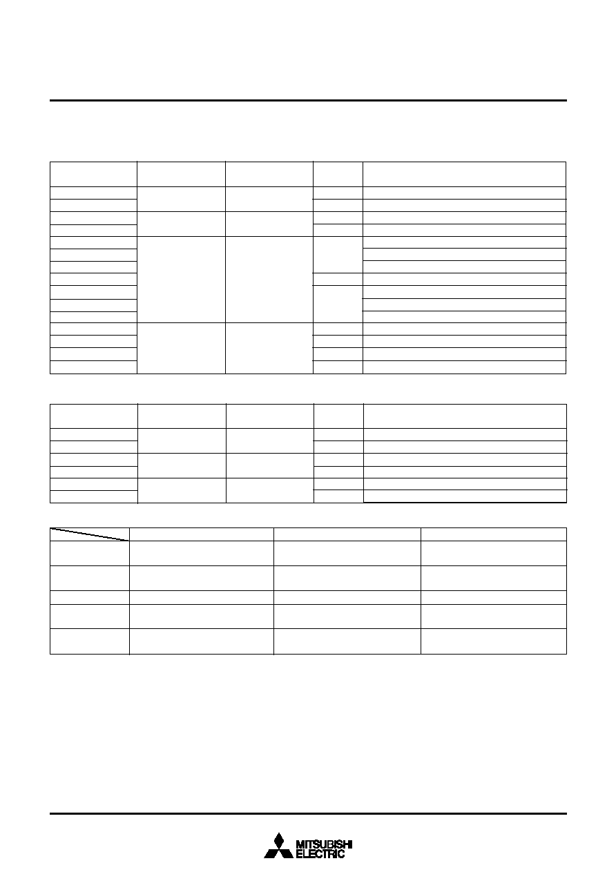
PIN CONFIGURATION (TOP VIEW)
Fig. 1 M38503MXH-XXXFP/SP pin configuration (spec. H)
q
Clock generating circuit ..................................... Built-in 2 circuits
(connect to external ceramic resonator or quartz-crystal oscillator)
q
Power source voltage
In high-speed mode .................................................. 4.0 to 5.5 V
(at 8 MHz oscillation frequency)
In middle-speed mode ............................................... 2.7 to 5.5 V
(at 8 MHz oscillation frequency)
In low-speed mode .................................................... 2.7 to 5.5 V
(at 32 kHz oscillation frequency)
q
Power dissipation
In high-speed mode .......................................................... 34 mW
(at 8 MHz oscillation frequency, at 5 V power source voltage)
In low-speed mode
Except M38507F8FP/SP ................................................... 60
µ
W
M38507F8FP/SP ............................................................. 450
µ
W
(at 32 kHz oscillation frequency, at 3 V power source voltage)
q
Operating temperature range .................................... ≠20 to 85∞C
APPLICATION
Office automation equipment, FA equipment, Household products,
Consumer electronics, etc.
Package type : FP ........................... 42P2R-A/E (42-pin plastic-molded SSOP)
Package type : SP ........................... 42P4B (42-pin plastic-molded SDIP)
P4
0
/CNTR
1
P
4
1
/
I
N
T
0
P
4
2
/
I
N
T
1
P
4
3
/
I
N
T
2
/
S
C
M
P
2
A
V
S
S
P
4
4
/
I
N
T
3
/
P
W
M
V
R
E
F
V
C
C
P
0
0
/
S
I
N
2
P
0
4
P
0
5
P
0
6
P
0
7
P
1
1
/
(
L
E
D
1
)
P
1
2
/
(
L
E
D
2
)
P
1
3
/
(
L
E
D
3
)
P
1
4
/
(
L
E
D
4
)
P
1
5
/
(
L
E
D
5
)
P
1
0
/
(
L
E
D
0
)
P
0
1
/
S
O
U
T
2
P
0
2
/
S
C
L
K
2
P
3
1
/
A
N
1
P
3
2
/
A
N
2
P
3
0
/
A
N
0
P
3
3
/
A
N
3
P
3
4
/
A
N
4
P
0
3
/
S
R
D
Y
2
4
0
41
4
2
2
2
23
2
4
25
2
6
27
2
8
29
3
0
3
1
3
2
34
35
3
6
3
7
38
39
33
3
2
1
2
1
20
1
9
18
1
7
16
1
5
14
1
3
1
2
1
1
9
8
7
6
5
4
10
M
3
8
5
0
3
M
X
H
-
X
X
X
F
P
/
S
P
P1
6
/(LED
6
)
P
1
7
/
(
L
E
D
7
)
P
2
7
/
C
N
T
R
0
/
S
R
D
Y
1
P
2
6
/
S
C
L
K
P2
5
/TxD
P
2
4
/
R
x
D
P
2
3
P
2
2
C
N
V
S
S
P
2
1
/
X
C
I
N
P
2
0
/
X
C
O
U
T
R
E
S
E
T
X
I
N
X
O
U
T
V
S
S
V
P
P
:
F
l
a
s
h
m
e
m
o
r
y
v
e
r
s
i
o
n
This data sheet describes Spec. H and Spec. A of 3850 Group. The header of each
page shows which specification is explained in the page. The page explaining about
both specifications shows the header of "Spec. H/A".
1

DESCRIPTION
The 3850 group (spec. A) is the 8-bit microcomputer based on the
740 family core technology.
The 3850 group (spec. A) is designed for the household products
and office automation equipment and includes serial I/O functions,
8-bit timer, and A-D converter.
FEATURES
q
Basic machine-language instructions ...................................... 71
q
Minimum instruction execution time ................................ 0.32
µ
s
(at 12.5 MHz oscillation frequency)
q
Memory size
ROM ................................................................... 8K to 16K bytes
RAM .............................................................................. 512 bytes
q
Programmable input/output ports ............................................ 34
q
On-chip software pull-up resistor
q
Interrupts ................................................. 15 sources, 14 vectors
q
Timers ............................................................................. 8-bit
4
q
Serial I/O1 .................... 8-bit
1(UART or Clock-synchronized)
q
Serial I/O2 ................................... 8-bit
1(Clock-synchronized)
q
PWM ............................................................................... 8-bit
1
q
A-D converter ............................................... 10-bit
9 channels
q
Watchdog timer ............................................................ 16-bit
1
PIN CONFIGURATION (TOP VIEW)
Fig. 2 M38503MXA-XXXFP/SP pin configuration (spec. A)
q
Clock generating circuit ..................................... Built-in 2 circuits
(connect to external ceramic resonator or quartz-crystal oscillator)
q
Power source voltage
In high-speed mode .................................................. 4.0 to 5.5 V
(at 12.5 MHz oscillation frequency)
In high-speed mode .................................................. 2.7 to 5.5 V
(at 6 MHz oscillation frequency)
In middle-speed mode ............................................... 2.7 to 5.5 V
(at 12.5 MHz oscillation frequency)
In low-speed mode .................................................... 2.7 to 5.5 V
(at 32 kHz oscillation frequency)
q
Power dissipation
In high-speed mode .......................................................... 34 mW
(at 12.5 MHz oscillation frequency, at 5 V power source voltage)
In low-speed mode
Except M38507F8FP/SP ................................................... 60
µ
W
M38507F8FP/SP ............................................................. 450
µ
W
(at 32 kHz oscillation frequency, at 3 V power source voltage)
q
Operating temperature range .................................... ≠20 to 85∞C
APPLICATION
Office automation equipment, FA equipment, Household products,
Consumer electronics, etc.
Package type : FP ........................... 42P2R-A/E (42-pin plastic-molded SSOP)
Package type : SP ........................... 42P4B (42-pin plastic-molded SDIP)
3850 Group (Spec. A)
SINGLE-CHIP 8-BIT CMOS MICROCOMPUTER
MITSUBISHI MICROCOMPUTERS
P
4
0
/
C
N
T
R
1
P
4
1
/
I
N
T
0
P
4
2
/
I
N
T
1
P
4
3
/
I
N
T
2
/
S
C
M
P
2
A
V
S
S
P
4
4
/
I
N
T
3
/
P
W
M
V
R
E
F
V
C
C
P
0
0
/
S
I
N
2
P
0
4
/
A
N
5
P
0
5
/
A
N
6
P
0
6
/
A
N
7
P
0
7
/
A
N
8
P
1
1
/
(
L
E
D
1
)
P
1
2
/
(
L
E
D
2
)
P
1
3
/
(
L
E
D
3
)
P
1
4
/
(
L
E
D
4
)
P
1
5
/
(
L
E
D
5
)
P
1
0
/
(
L
E
D
0
)
P
0
1
/
S
O
U
T
2
P
0
2
/
S
C
L
K
2
P
3
1
/
A
N
1
P
3
2
/
A
N
2
P
3
0
/
A
N
0
P
3
3
/
A
N
3
P
3
4
/
A
N
4
P
0
3
/
S
R
D
Y
2
4
0
41
4
2
2
2
23
2
4
25
2
6
27
2
8
29
3
0
3
1
3
2
34
35
3
6
3
7
38
39
33
3
2
1
2
1
20
1
9
18
1
7
16
1
5
14
1
3
1
2
1
1
9
8
7
6
5
4
10
M
3
8
5
0
3
M
X
A
-
X
X
X
F
P
/
S
P
P1
6
/(LED
6
)
P
1
7
/
(
L
E
D
7
)
P
2
7
/
C
N
T
R
0
/
S
R
D
Y
1
P
2
6
/
S
C
L
K
P2
5
/TxD
P
2
4
/
R
x
D
P
2
3
P
2
2
C
N
V
S
S
P
2
1
/
X
C
I
N
P
2
0
/
X
C
O
U
T
R
E
S
E
T
X
I
N
X
O
U
T
V
S
S
V
P
P
:
F
l
a
s
h
m
e
m
o
r
y
v
e
r
s
i
o
n
2
3850 Group (Spec. H)
SINGLE-CHIP 8-BIT CMOS MICROCOMPUTER
MITSUBISHI MICROCOMPUTERS
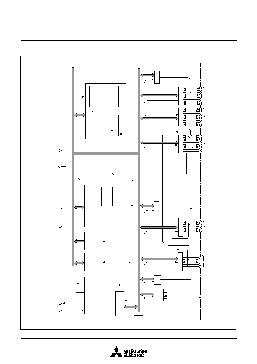
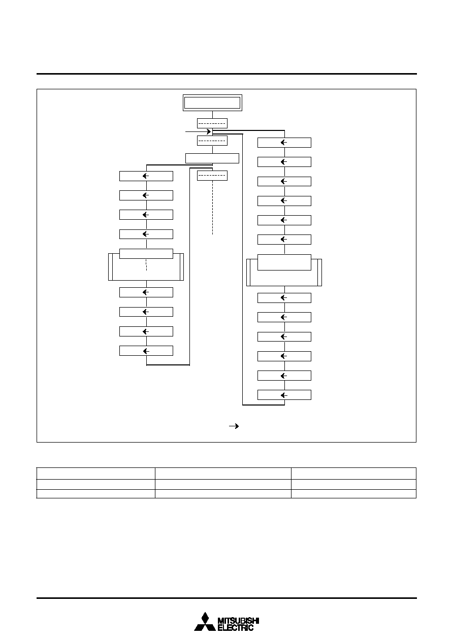
FUNCTIONAL BLOCK DIAGRAM
Fig. 3 Functional block diagram (spec. H)
FUNCTIONAL BLOCK
I
N
T
0
≠
V
R
E
F
A
V
S
S
R
A
M
R
O
M
C
P
U
A
X
Y
S
P
C
H
P
C
L
P
S
V
S
S
2
1
R
E
S
E
T
1
8
V
C
C
1
1
5
C
N
V
S
S
2
3
X
I
N
1
9
2
0
S
I
/
O
1
(
8
)
R
e
s
e
t
i
n
p
u
t
C
l
o
c
k
g
e
n
e
r
a
t
i
n
g
c
i
r
c
u
i
t
M
a
i
n
-
c
l
o
c
k
i
n
p
u
t
M
a
i
n
-
c
l
o
c
k
o
u
t
p
u
t
A
-
D
c
o
n
v
e
r
t
e
r
(
1
0
)
C
N
T
R
0
C
N
T
R
1
T
i
m
e
r
Y
(
8
)
T
i
m
e
r
X
(
8
)
P
r
e
s
c
a
l
e
r
1
2
(
8
)
P
r
e
s
c
a
l
e
r
X
(
8
)
P
r
e
s
c
a
l
e
r
Y
(
8
)
T
i
m
e
r
1
(
8
)
T
i
m
e
r
2
(
8
)
S
u
b
-
c
l
o
c
k
i
n
p
u
t
X
O
U
T
X
C
I
N
X
C
O
U
T
S
u
b
-
c
l
o
c
k
o
u
t
p
u
t
W
a
t
c
h
d
o
g
t
i
m
e
r
R
e
s
e
t
P
2
(
8
)
P
3
(
5
)
I
/
O
p
o
r
t
P
2
I
/
O
p
o
r
t
P
3
P
4
(
5
)
I
/
O
p
o
r
t
P
4
I
N
T
3
4
6
8
5
7
3
9
4
1
3
8
4
0
4
2
9
1
1
1
3
1
7
1
0
1
2
1
4
1
6
P
1
(
8
)
I
/
O
p
o
r
t
P
1
2
2
2
4
2
6
2
8
2
3
2
5
2
7
2
9
P
0
(
8
)
I
/
O
p
o
r
t
P
0
3
0
3
1
3
2
3
3
3
4
3
5
3
6
3
7
P
W
M
(
8
)
X
C
I
N
X
C
O
U
T
S
I
/
O
2
(
8
)
3

4
SINGLE-CHIP 8-BIT CMOS MICROCOMPUTER
MITSUBISHI MICROCOMPUTERS
FUNCTIONAL BLOCK DIAGRAM
Fig. 4 Functional block diagram (spec. A)
3850 Group (Spec. A)
INT
0
≠
V
REF
AV
SS
R A M
R O M
C P U
A
X
Y
S
PC
H
PC
L
PS
V
SS
21
RESET
18
V
CC
1
15
CNV
SS
23
X
IN
19
20
SI/O1(8)
Reset input
Clock generating circuit
Main-clock
input
Main-clock
output
A-D
converter
(10)
CNTR
0
CNTR
1
Timer Y( 8 )
Timer X( 8 )
Prescaler 12(8)
Prescaler X(8)
Prescaler Y(8)
Timer 1( 8 )
Timer 2( 8 )
Sub-clock
input
X
OUT
X
CIN
X
COUT
Sub-clock
output
Watchdog
timer
Reset
P2(8)
P3(5)
I/O port P2
I/O port P3
P4(5)
I/O port P4
INT
3
4
6
8
5
7
39
41
38
40
42
9
11
13
17
10
12
14
16
P1(8)
I/O port P1
22
24
26
28
23
25
27
29
P0(8)
I/O port P0
30
31
32
33
34
35
36
37
PWM
(8)
X
CIN
X
COUT
SI/O2(8)

5
SINGLE-CHIP 8-BIT CMOS MICROCOMPUTER
MITSUBISHI MICROCOMPUTERS
3850 Group (Spec. H)
V
CC
, V
SS
Functions
Name
Pin
∑Apply voltage of 2.7 V ≠ 5.5 V to Vcc, and 0 V to Vss.
∑This pin controls the operation mode of the chip.
∑Normally connected to V
SS
.
∑Reset input pin for active "L."
∑Input and output pins for the clock generating circuit.
∑Connect a ceramic resonator or quartz-crystal oscillator between the X
IN
and X
OUT
pins to set
the oscillation frequency.
∑When an external clock is used, connect the clock source to the X
IN
pin and leave the X
OUT
pin open.
∑8-bit CMOS I/O port.
∑I/O direction register allows each pin to be individually
programmed as either input or output.
∑CMOS compatible input level.
∑CMOS 3-state output structure.
∑P1
0
to P1
7
(8 bits) are enabled to output large current for LED drive.
Power source
Table 1 Pin description (spec. H)
Function except a port function
Clock input
Clock output
I/O port P0
CNV
SS
input
CNV
SS
RESET
Reset input
X
IN
X
OUT
P0
0
/S
IN2
P0
1
/S
OUT2
P0
2
/S
CLK2
P0
3
/S
RDY2
P0
4
≠P0
7
I/O port P1
P1
0
≠P1
7
∑ Serial I/O2 function pin
∑ Sub-clock generating circuit I/O
pins (connect a resonator)
I/O port P2
I/O port P3
I/O port P4
∑8-bit CMOS I/O port.
∑I/O direction register allows each pin to be individually
programmed as either input or output.
∑CMOS compatible input level.
∑P2
0
, P2
1
, P2
4
to P2
7
: CMOS3-state output structure.
∑P2
2
, P2
3
: N-channel open-drain structure.
∑ Serial I/O1 function pin
∑ Serial I/O1 function pin/
Timer X function pin
∑ A-D converter input pin
∑ Timer Y function pin
∑ Interrupt input pins
∑ Interrupt input pin
∑ S
CMP2
output pin
∑ Interrupt input pin
∑ PWM output pin
∑8-bit CMOS I/O port with the same function as port P0.
∑CMOS compatible input level.
∑CMOS 3-state output structure.
∑8-bit CMOS I/O port with the same function as port P0.
∑CMOS compatible input level.
∑CMOS 3-state output structure.
P2
0
/X
COUT
P2
1
/X
CIN
P2
2
P2
3
P2
4
/RxD
P2
5
/TxD
P2
6
/S
CLK
P2
7
/CNTR
0
/
S
RDY1
P3
0
/AN
0
≠
P3
4
/AN
4
P4
0
/CNTR
1
P4
1
/INT
0
P4
2
/INT
1
P4
3
/INT
2
/S
CMP2
P4
4
/INT
3
/PWM
6
SINGLE-CHIP 8-BIT CMOS MICROCOMPUTER
MITSUBISHI MICROCOMPUTERS
3850 Group (Spec. A)
V
CC
, V
SS
Functions
Name
Pin
∑Apply voltage of 2.7 V ≠ 5.5 V to Vcc, and 0 V to Vss.
∑This pin controls the operation mode of the chip.
∑Normally connected to V
SS
.
∑Reset input pin for active "L."
∑Input and output pins for the clock generating circuit.
∑Connect a ceramic resonator or quartz-crystal oscillator between the X
IN
and X
OUT
pins to set
the oscillation frequency.
∑When an external clock is used, connect the clock source to the X
IN
pin and leave the X
OUT
pin open.
∑8-bit CMOS I/O port.
∑I/O direction register allows each pin to be individually
programmed as either input or output.
∑CMOS compatible input level.
∑CMOS 3-state output structure.
∑Pull-up control is enabled in a byte unit.
∑P1
0
to P1
7
(8 bits) are enabled to output large current
Power source
Table 2 Pin description (spec. A)
Function except a port function
Clock input
Clock output
I/O port P0
CNV
SS
input
CNV
SS
RESET
Reset input
X
IN
X
OUT
P0
0
/S
IN2
P0
1
/S
OUT2
P0
2
/S
CLK2
P0
3
/S
RDY2
P0
4
/AN
5
≠P0
7
/AN
8
I/O port P1
P1
0
≠P1
7
∑ Serial I/O2 function pin
∑ Sub-clock generating circuit I/O
pins (connect a resonator)
I/O port P2
I/O port P3
I/O port P4
for LED drive.
∑8-bit CMOS I/O port.
∑I/O direction register allows each pin to be individually
programmed as either input or output.
∑CMOS compatible input level.
∑P2
0
, P2
1
, P2
4
to P2
7
: CMOS3-state output structure.
∑P2
2
, P2
3
: N-channel open-drain structure.
∑Pull-up control of P2
0
, P2
1
, P2
4
≠P2
7
is enabled in a
byte unit.
∑ Serial I/O1 function pin
∑ Serial I/O1 function pin/
Timer X function pin
∑ A-D converter input pin
∑ Timer Y function pin
∑ Interrupt input pins
∑ Interrupt input pin
∑ S
CMP2
output pin
∑ Interrupt input pin
∑ PWM output pin
∑8-bit CMOS I/O port with the same function as port P0.
∑CMOS compatible input level.
∑CMOS 3-state output structure.
∑Pull-up control is enabled in a bit unit.
∑8-bit CMOS I/O port with the same function as port P0.
∑CMOS compatible input level.
∑CMOS 3-state output structure.
∑Pull-up control is enabled in a bit unit.
P2
0
/X
COUT
P2
1
/X
CIN
P2
2
P2
3
P2
4
/RxD
P2
5
/TxD
P2
6
/S
CLK
P2
7
/CNTR
0
/
S
RDY1
P3
0
/AN
0
≠
P3
4
/AN
4
P4
0
/CNTR
1
P4
1
/INT
0
P4
2
/INT
1
P4
3
/INT
2
/S
CMP2
P4
4
/INT
3
/PWM
∑ A-D converter input pin
7
SINGLE-CHIP 8-BIT CMOS MICROCOMPUTER
MITSUBISHI MICROCOMPUTERS
PART NUMBERING
3850 Group (Spec. H/A)
Fig. 5 Part numbering
M3850 3
M
4
A≠ XXX
SP
Product name
Package type
SP : 42P4B
FP : 42P2R-A/E
SS : 42S1B-A
ROM number
Omitted in One Time PROM version shipped in blank,
EPROM version, and flash memory version.
ROM/PROM/Flash memory size
1
2
3
4
5
6
7
8
: 4096 bytes
: 8192 bytes
: 12288 bytes
: 16384 bytes
: 20480 bytes
: 24576 bytes
: 28672 bytes
: 32768 bytes
The first 128 bytes and the last 2 bytes of ROM are reserved areas ; they
cannot be used as a user's ROM area.
However, they can be programmed or erased in the flash memory version,
so that the users can use them.
Memory type
M : Mask ROM version
E : EPROM or One Time PROM version
F : Flash memory version
RAM size
0
1
2
3
4
: 192 bytes
: 256 bytes
: 384 bytes
: 512 bytes
: 640 bytes
≠ : standard
Omitted in One Time PROM version shipped in blank, EPROM
version, and flash memory version.
H≠: Partial specification changed version
A≠: High-speed version
: 36864 bytes
: 40960 bytes
: 45056 bytes
: 49152 bytes
: 53248 bytes
: 57344 bytes
: 61440 bytes
9
A
B
C
D
E
F
5
6
7
8
9
: 768 bytes
: 896 bytes
: 1024 bytes
: 1536 bytes
: 2048 bytes
8
SINGLE-CHIP 8-BIT CMOS MICROCOMPUTER
MITSUBISHI MICROCOMPUTERS
GROUP EXPANSION
Mitsubishi plans to expand the 3850 group (spec. H/A) as follows.
Memory Type
Support for mask ROM, One Time PROM, and flash memory ver-
sions.
Memory Size
Flash memory size ......................................................... 32 K bytes
Mask ROM size ................................... 8 K to 32 K bytes (spec. H)
8 K to 16 K bytes (spec. A)
RAM size ............................................... 512 to 1 K bytes (spec. H)
512 bytes (spec. A)
Packages
42P4B ......................................... 42-pin shrink plastic-molded DIP
42P2R-A/E ........................................... 42-pin plastic-molded SOP
42S1B-A .................. 42-pin shrink ceramic DIP (EPROM version)
Fig. 6 Memory expansion plan
Memory Expansion Plan
3850 Group (Spec. H/A)
32K
2
8
K
2
4
K
2
0
K
1
6
K
1
2
K
8K
3
8
4
5
1
2
6
4
0
7
6
8
896
1
0
2
4
1
1
5
2
1
2
8
0
1
4
0
8
1536
2048
R
O
M
e
x
t
e
r
a
n
a
l
R
O
M
s
i
z
e
(
b
y
t
e
s
)
RAM size (bytes)
M
3
8
5
0
7
M
8
/
F
8
M38504M6/E6
M38503M4H
P
r
o
d
u
c
t
s
u
n
d
e
r
d
e
v
e
l
o
p
m
e
n
t
o
r
p
l
a
n
n
i
n
g
:
t
h
e
d
e
v
e
l
o
p
m
e
n
t
s
c
h
e
d
u
l
e
a
n
d
s
p
e
c
i
f
i
c
a
t
i
o
n
m
a
y
b
e
r
e
v
i
s
e
d
w
i
t
h
o
u
t
n
o
t
i
c
e
.
T
h
e
d
e
v
e
l
o
p
m
e
n
t
o
f
pl
a
n
n
i
n
g
p
r
o
d
u
c
t
s
m
a
y
b
e
s
t
o
p
p
e
d
.
M
a
s
s
p
r
o
d
u
c
t
i
o
n
M
a
s
s
p
r
o
d
u
c
t
i
o
n
M
a
s
s
p
r
o
d
u
c
t
i
o
n
M
3
8
5
0
3
M
4
A
M
a
s
s
p
r
o
d
u
c
t
i
o
n
M38503M2H
M
3
8
5
0
3
M
2
A
Mass production
Mass production
9
SINGLE-CHIP 8-BIT CMOS MICROCOMPUTER
MITSUBISHI MICROCOMPUTERS
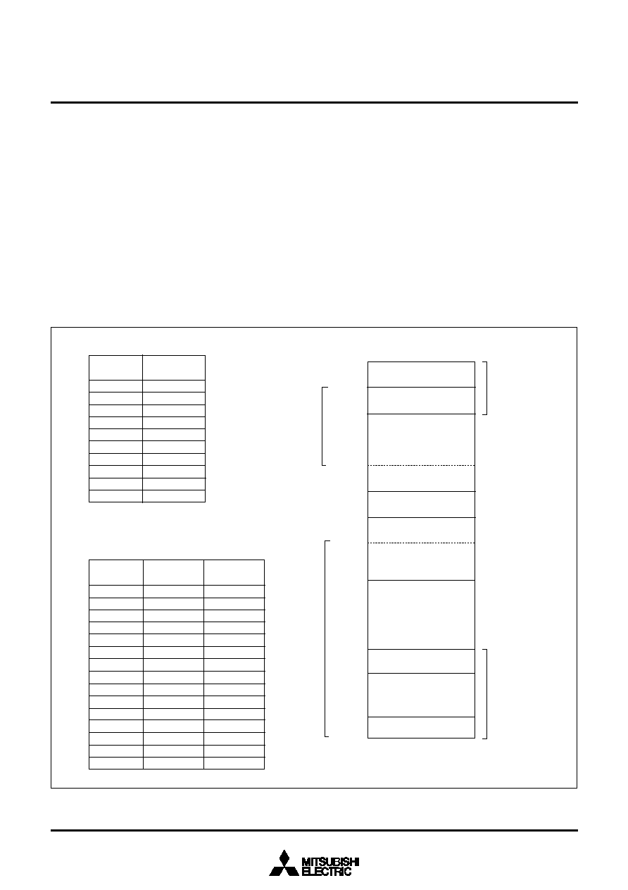
Currently planning products are listed below.
RAM size (bytes)
Remarks
Package
Table 3 Support products (spec. H)
Product name
24576
(24446)
ROM size (bytes)
ROM size for User in ( )
M38503M2H-XXXSP
M38503M2H-XXXFP
M38503M4H-XXXSP
M38503M4H-XXXFP
M38504M6-XXXSP
M38504E6-XXXSP
M38504E6SP
M38504E6SS
M38504M6-XXXFP
M38504E6-XXXFP
M38504E6FP
M38507M8-XXXSP
M38507M8-XXXFP
M38507F8SP
M38507F8FP
42P4B
42P2R-A/E
42P4B
42P2R-A/E
424P4B
42S1B-A
42P2R-A/E
42P4B
42P2R-A/E
42P4B
42P2R-A/E
Mask ROM version
Mask ROM version
Mask ROM version
Mask ROM version
Mask ROM version
One Time PROM version
One Time PROM version (blank)
EPROM version
Mask ROM version
One Time PROM version
One Time PROM version (blank)
Mask ROM version
Mask ROM version
Flash memory version
Flash memory version
8192
(8062)
512
16384
(16254)
640
512
Table 5 Differences among 3850 group (standard), 3850 group (spec. H), and 3850 group (spec. A)
Serial I/O
A-D converter
Large current port
Software pull-up
resistor
Maximum operating
frequency
3850 group (standard)
1: Serial I/O
(UART or Clock-synchronized)
Unserviceable in low-speed mode
Analog channel ............................. 5
5: P1
3
≠P1
7
Not available
8 MHz
3850 group (spec. H)
2: Serial I/O1 (UART or Clock-synchronized)
Serial I/O2 (Clock-synchronized)
Serviceable in low-speed mode
Analog channel ................................ 5
8: P1
0
≠P1
7
Not available
8 MHz
3850 Group (Spec. H/A)
32768
(32638)
1024
RAM size (bytes)
Remarks
Package
Table 4 Support products (spec. A)
Product name
ROM size (bytes)
ROM size for User in ( )
M38503M2A-XXXSP
M38503M2A-XXXFP
M38503M4A-XXXSP
M38503M4A-XXXFP
M38507F8SP
M38507F8FP
42P4B
42P2R-A/E
42P4B
42P2R-A/E
42P4B
42P2R-A/E
Mask ROM version
Mask ROM version
Mask ROM version
Mask ROM version
Flash memory version
Flash memory version
8192
(8062)
512
16384
(16254)
512
32768
1024
3850 group (spec. A)
2: Serial I/O1 (UART or Clock-synchronized)
Serial I/O2 (Clock-synchronized)
Serviceable in low-speed mode
Analog channel ................................ 9
8: P1
0
≠P1
7
Built-in (Port P0≠P4)
12.5 MHz
Notes on differences among 3850 group
(standard), 3850 group (spec. H), and 3850
group (spec. A)
(1) The absolute maximum ratings of 3850 group (spec. H/A) is
smaller than that of 3850 group (standard).
∑Power source voltage Vcc = ≠0.3 to 6.5 V
∑CNVss input voltage V
I
= ≠0.3 to Vcc +0.3 V
(2) The oscillation circuit constants of X
IN
-X
OUT
, X
CIN
-X
COUT
may
be some differences among 3850 group (standard), 3850
group (spec. H), and 3850 group (spec. A).
(3) Do not write any data to the reserved area and the reserved
bit. (Do not change the contents after reset.)
(4) Fix bit 3 of the CPU mode register to "1".
(5) Be sure to perform the termination of unused pins.

10
SINGLE-CHIP 8-BIT CMOS MICROCOMPUTER
MITSUBISHI MICROCOMPUTERS
FUNCTIONAL DESCRIPTION
CENTRAL PROCESSING UNIT (CPU)
The 3850 group (spec. H/A) uses the standard 740 Family instruc-
tion set. Refer to the table of 740 Family addressing modes and
machine instructions or the 740 Family Software Manual for de-
tails on the instruction set.
Machine-resident 740 Family instructions are as follows:
The FST and SLW instructions cannot be used.
The STP, WIT, MUL, and DIV instructions can be used.
[Accumulator (A)]
The accumulator is an 8-bit register. Data operations such as data
transfer, etc., are executed mainly through the accumulator.
[Index Register X (X)]
The index register X is an 8-bit register. In the index addressing
modes, the value of the OPERAND is added to the contents of
register X and specifies the real address.
[Index Register Y (Y)]
The index register Y is an 8-bit register. In partial instruction, the
value of the OPERAND is added to the contents of register Y and
specifies the real address.
[Stack Pointer (S)]
The stack pointer is an 8-bit register used during subroutine calls
and interrupts. This register indicates start address of stored area
(stack) for storing registers during subroutine calls and interrupts.
The low-order 8 bits of the stack address are determined by the
contents of the stack pointer. The high-order 8 bits of the stack ad-
dress are determined by the stack page selection bit. If the stack
page selection bit is "0" , the high-order 8 bits becomes "00
16
". If
the stack page selection bit is "1", the high-order 8 bits becomes
"01
16
".
The operations of pushing register contents onto the stack and
popping them from the stack are shown in Figure 8.
Store registers other than those described in Figure 8 with pro-
gram when the user needs them during interrupts or subroutine
calls.
[Program Counter (PC)]
The program counter is a 16-bit counter consisting of two 8-bit
registers PC
H
and PC
L
. It is used to indicate the address of the
next instruction to be executed.
Fig. 7 740 Family CPU register structure
3850 Group (Spec. H/A)
A
Accumulator
b7
b7
b7
b7
b0
b7
b15
b0
b7
b0
b0
b0
b0
X
Index register X
Y
Index register Y
S
Stack pointer
PC
L
Program counter
PC
H
N V T B D I Z C
Processor status register (PS)
Carry flag
Zero flag
Interrupt disable flag
Decimal mode flag
Break flag
Index X mode flag
Overflow flag
Negative flag
11
SINGLE-CHIP 8-BIT CMOS MICROCOMPUTER
MITSUBISHI MICROCOMPUTERS
Table 6 Push and pop instructions of accumulator or processor status register
Accumulator
Processor status register
Push instruction to stack
PHA
PHP
Pop instruction from stack
PLA
PLP
Fig. 8 Register push and pop at interrupt generation and subroutine call
3850 Group (Spec. H/A)
N
o
t
e:
C
o
n
d
i
t
i
o
n
f
o
r
a
c
c
e
p
t
a
n
c
e
o
f
a
n
i
n
t
e
r
r
u
p
t
I
n
t
e
r
r
u
p
t
e
n
a
b
l
e
f
l
a
g
i
s
"
1
"
E
x
e
c
u
t
e
J
S
R
O
n
-
g
o
i
n
g
R
o
u
t
i
n
e
M
(
S
)
(
P
C
H
)
(
S
)
(
S
)
≠
1
M
(
S
)
(
P
C
L
)
E
x
e
c
u
t
e
R
T
S
(
P
C
L
)
M
(
S
)
(
S
)
(
S
)
≠
1
(S)
(S) + 1
(
S
)
(
S
)
+
1
(PC
H
)
M (S)
S
u
b
r
o
u
t
i
n
e
P
O
P
r
e
t
u
r
n
a
d
d
r
e
s
s
f
r
o
m
s
t
a
c
k
P
u
s
h
r
e
t
u
r
n
a
d
d
r
e
s
s
o
n
s
t
a
c
k
M
(
S
)
(
P
S
)
E
x
e
c
u
t
e
R
T
I
(
P
S
)
M
(
S
)
(S)
(S) ≠ 1
(
S
)
(
S
)
+
1
I
n
t
e
r
r
u
p
t
S
e
r
v
i
c
e
R
o
u
t
i
n
e
P
O
P
c
o
n
t
e
n
t
s
o
f
p
r
o
c
e
s
s
o
r
s
t
a
t
u
s
r
e
g
i
s
t
e
r
f
r
o
m
s
t
a
c
k
M
(
S
)
(
P
C
H
)
(
S
)
(
S
)
≠
1
M
(
S
)
(
P
C
L
)
(
S
)
(
S
)
≠
1
(
P
C
L
)
M
(
S
)
(
S
)
(
S
)
+
1
(
S
)
(
S
)
+
1
(PC
H
)
M (S)
P
O
P
r
e
t
u
r
n
a
d
d
r
e
s
s
f
r
o
m
s
t
a
c
k
I
F
l
a
g
i
s
s
e
t
f
r
o
m
"
0
"
t
o
"
1
"
F
e
t
c
h
t
h
e
j
u
m
p
v
e
c
t
o
r
P
u
s
h
r
e
t
u
r
n
a
d
d
r
e
s
s
o
n
s
t
a
c
k
P
u
s
h
c
o
n
t
e
n
t
s
o
f
p
r
o
c
e
s
s
o
r
s
t
a
t
u
s
r
e
g
i
s
t
e
r
o
n
s
t
a
c
k
I
n
t
e
r
r
u
p
t
r
e
q
u
e
s
t
(
N
o
t
e
)
Interrupt disable flag is "0"

12
SINGLE-CHIP 8-BIT CMOS MICROCOMPUTER
MITSUBISHI MICROCOMPUTERS
∑Bit 4: Break flag (B)
The B flag is used to indicate that the current interrupt was
generated by the BRK instruction. The BRK flag in the processor
status register is always "0". When the BRK instruction is used to
generate an interrupt, the processor status register is pushed
onto the stack with the break flag set to "1".
∑Bit 5: Index X mode flag (T)
When the T flag is "0", arithmetic operations are performed
between accumulator and memory. When the T flag is "1", direct
arithmetic operations and direct data transfers are enabled
between memory locations.
∑Bit 6: Overflow flag (V)
The V flag is used during the addition or subtraction of one byte
of signed data. It is set if the result exceeds +127 to -128. When
the BIT instruction is executed, bit 6 of the memory location
operated on by the BIT instruction is stored in the overflow flag.
∑Bit 7: Negative flag (N)
The N flag is set if the result of an arithmetic operation or data
transfer is negative. When the BIT instruction is executed, bit 7 of
the memory location operated on by the BIT instruction is stored
in the negative flag.
Table 7 Set and clear instructions of each bit of processor status register
Set instruction
Clear instruction
C flag
Z flag
I flag
D flag
B flag
T flag
V flag
N flag
SEC
CLC
_
_
SEI
CLI
SED
CLD
_
_
SET
CLT
CLV
_
_
_
[Processor status register (PS)]
The processor status register is an 8-bit register consisting of 5
flags which indicate the status of the processor after an arithmetic
operation and 3 flags which decide MCU operation. Branch opera-
tions can be performed by testing the Carry (C) flag , Zero (Z) flag,
Overflow (V) flag, or the Negative (N) flag. In decimal mode, the Z,
V, N flags are not valid.
∑Bit 0: Carry flag (C)
The C flag contains a carry or borrow generated by the arithmetic
logic unit (ALU) immediately after an arithmetic operation. It can
also be changed by a shift or rotate instruction.
∑Bit 1: Zero flag (Z)
The Z flag is set if the result of an immediate arithmetic operation
or a data transfer is "0", and cleared if the result is anything other
than "0".
∑Bit 2: Interrupt disable flag (I)
The I flag disables all interrupts except for the interrupt
generated by the BRK instruction.
Interrupts are disabled when the I flag is "1".
∑Bit 3: Decimal mode flag (D)
The D flag determines whether additions and subtractions are
executed in binary or decimal. Binary arithmetic is executed when
this flag is "0"; decimal arithmetic is executed when it is "1".
Decimal correction is automatic in decimal mode. Only the ADC
and SBC instructions can be used for decimal arithmetic.
3850 Group (Spec. H/A)

13
SINGLE-CHIP 8-BIT CMOS MICROCOMPUTER
MITSUBISHI MICROCOMPUTERS
[CPU Mode Register (CPUM)] 003B
16
The CPU mode register contains the stack page selection bit, etc.
The CPU mode register is allocated at address 003B
16
.
Fig. 9 Structure of CPU mode register
3850 Group (Spec. H/A)
C
P
U
m
o
d
e
r
e
g
i
s
t
e
r
(
C
P
U
M
:
a
d
d
r
e
s
s
0
0
3
B
1
6
)
b
7
b
0
Stack page selection bit
0 : 0 page
1 : 1 page
F
i
x
t
h
i
s
b
i
t
t
o
"
1
"
.
P
r
o
c
e
s
s
o
r
m
o
d
e
b
i
t
s
b
1
b
0
0
0
:
S
i
n
g
l
e
-
c
h
i
p
m
o
d
e
0
1
:
1
0
:
N
o
t
a
v
a
i
l
a
b
l
e
1
1
:
P
o
r
t
X
C
s
w
i
t
c
h
b
i
t
0
:
I
/
O
p
o
r
t
f
u
n
c
t
i
o
n
(
s
t
o
p
o
s
c
i
l
l
a
t
i
n
g
)
1
:
X
C
I
N
≠
X
C
O
U
T
o
s
c
i
l
l
a
t
i
n
g
f
u
n
c
t
i
o
n
M
a
i
n
c
l
o
c
k
(
X
I
N
≠
X
O
U
T
)
s
t
o
p
b
i
t
0
:
O
s
c
i
l
l
a
t
i
n
g
1
:
S
t
o
p
p
e
d
M
a
i
n
c
l
o
c
k
d
i
v
i
s
i
o
n
r
a
t
i
o
s
e
l
e
c
t
i
o
n
b
i
t
s
b
7
b
6
0
0
:
=
f
(
X
I
N
)
/
2
(
h
i
g
h
-
s
p
e
e
d
m
o
d
e
)
0
1
:
=
f
(
X
I
N
)
/
8
(
m
i
d
d
l
e
-
s
p
e
e
d
m
o
d
e
)
1
0
:
=
f
(
X
C
I
N
)
/
2
(
l
o
w
-
s
p
e
e
d
m
o
d
e
)
1
1
:
N
o
t
a
v
a
i
l
a
b
l
e
1
14
SINGLE-CHIP 8-BIT CMOS MICROCOMPUTER
MITSUBISHI MICROCOMPUTERS
3850 Group (Spec. H/A)
MEMORY
Special Function Register (SFR) Area
The Special Function Register area in the zero page contains
control registers such as I/O ports and timers.
RAM
RAM is used for data storage and for stack area of subroutine
calls and interrupts.
ROM
The first 128 bytes and the last 2 bytes of ROM are reserved for
device testing and the rest is user area for storing programs.
Interrupt Vector Area
The interrupt vector area contains reset and interrupt vectors.
Zero Page
Access to this area with only 2 bytes is possible in the zero page
addressing mode.
Special Page
Access to this area with only 2 bytes is possible in the special
page addressing mode.
Fig. 10 Memory map diagram
0
1
0
0
1
6
0000
16
0040
16
FF00
16
F
F
D
C
1
6
FFFE
16
FFFF
16
1
9
2
2
5
6
3
8
4
5
1
2
6
4
0
7
6
8
8
9
6
1
0
2
4
1
5
3
6
2
0
4
8
XXXX
16
0
0
F
F
1
6
0
1
3
F
1
6
0
1
B
F
1
6
0
2
3
F
1
6
0
2
B
F
1
6
0
3
3
F
1
6
0
3
B
F
1
6
0
4
3
F
1
6
0
6
3
F
1
6
0
8
3
F
1
6
4
0
9
6
8
1
9
2
1
2
2
8
8
1
6
3
8
4
2
0
4
8
0
2
4
5
7
6
2
8
6
7
2
3
2
7
6
8
3
6
8
6
4
4
0
9
6
0
4
5
0
5
6
4
9
1
5
2
5
3
2
4
8
5
7
3
4
4
6
1
4
4
0
F
0
0
0
1
6
E
0
0
0
1
6
D
0
0
0
1
6
C
0
0
0
1
6
B
0
0
0
1
6
A
0
0
0
1
6
9
0
0
0
1
6
8
0
0
0
1
6
7
0
0
0
1
6
6
0
0
0
1
6
5
0
0
0
1
6
4
0
0
0
1
6
3
0
0
0
1
6
2
0
0
0
1
6
1
0
0
0
1
6
F080
16
E080
16
D080
16
C080
16
B080
16
A080
16
9080
16
8080
16
7080
16
6080
16
5080
16
4080
16
3080
16
2080
16
1080
16
YYYY
16
ZZZZ
16
RAM
ROM
0FF0
16
0FFF
16
S
F
R
a
r
e
a
N
o
t
u
s
e
d
Interrupt vector area
R
O
M
a
r
e
a
R
e
s
e
r
v
e
d
R
O
M
a
r
e
a
(
1
2
8
b
y
t
e
s
)
Z
e
r
o
p
a
g
e
Special page
R
A
M
a
r
e
a
R
A
M
s
i
z
e
(
b
y
t
e
s
)
A
d
d
r
e
s
s
X
X
X
X
1
6
R
O
M
s
i
z
e
(
b
y
t
e
s
)
Address
YYYY
16
R
e
s
e
r
v
e
d
R
O
M
a
r
e
a
Address
ZZZZ
16
Not used
SFR area (Note)
Note: Flash memory version only

15
SINGLE-CHIP 8-BIT CMOS MICROCOMPUTER
MITSUBISHI MICROCOMPUTERS
3850 Group (Spec. H)
Fig. 11 Memory map of special function register (SFR) (spec. H)
0020
16
0021
16
0022
16
0023
16
0024
16
0025
16
0026
16
0027
16
0028
16
0029
16
002A
16
002B
16
002C
16
002D
16
002E
16
002F
16
0030
16
0031
16
0032
16
0033
16
0034
16
0035
16
0036
16
0037
16
0038
16
0039
16
003A
16
003B
16
003C
16
003D
16
003E
16
003F
16
0
0
0
0
1
6
0
0
0
1
1
6
0
0
0
2
1
6
0
0
0
3
1
6
0
0
0
4
1
6
0005
16
0006
16
0
0
0
7
1
6
0
0
0
8
1
6
0
0
0
9
1
6
0
0
0
A
1
6
0
0
0
B
1
6
0
0
0
C
1
6
0
0
0
D
1
6
000E
16
000F
16
0010
16
0011
16
0012
16
0013
16
0014
16
0015
16
0016
16
0017
16
0018
16
0019
16
001A
16
001B
16
001C
16
001D
16
0
0
1
E
1
6
0
0
1
F
1
6
P
o
r
t
P
0
(
P
0
)
P
o
r
t
P
0
d
i
r
e
c
t
i
o
n
r
e
g
i
s
t
e
r
(
P
0
D
)
P
o
r
t
P
1
(
P
1
)
P
o
r
t
P
1
d
i
r
e
c
t
i
o
n
r
e
g
i
s
t
e
r
(
P
1
D
)
P
o
r
t
P
2
(
P
2
)
P
o
r
t
P
2
d
i
r
e
c
t
i
o
n
r
e
g
i
s
t
e
r
(
P
2
D
)
P
o
r
t
P
3
(
P
3
)
P
o
r
t
P
3
d
i
r
e
c
t
i
o
n
r
e
g
i
s
t
e
r
(
P
3
D
)
P
o
r
t
P
4
(
P
4
)
P
o
r
t
P
4
d
i
r
e
c
t
i
o
n
r
e
g
i
s
t
e
r
(
P
4
D
)
Transmit/Receive buffer register (TB/RB)
Serial I/O1 status register (SIOSTS)
Serial I/O1 control register (SIOCON)
UART control register (UARTCON)
B
a
u
d
r
a
t
e
g
e
n
e
r
a
t
o
r
(
B
R
G
)
Interrupt control register 2 (ICON2)
A-D conversion low-order register (ADL)
Prescaler Y (PREY)
Timer Y (TY)
A-D control register (ADCON)
A-D conversion high-order register (ADH)
Interrupt edge selection register (INTEDGE)
CPU mode register (CPUM)
Interrupt request register 1 (IREQ1)
Interrupt request register 2 (IREQ2)
Interrupt control register 1 (ICON1)
Prescaler 12 (PRE12)
Timer 2 (T2)
Prescaler X (PREX)
Timer X (TX)
Timer 1 (T1)
Timer XY mode register (TM)
Reserved
MISRG
Watchdog timer control register (WDTCON)
P
W
M
c
o
n
t
r
o
l
r
e
g
i
s
t
e
r
(
P
W
M
C
O
N
)
P
W
M
p
r
e
s
c
a
l
e
r
(
P
R
E
P
W
M
)
PWM register (PWM)
T
i
m
e
r
c
o
u
n
t
s
o
u
r
c
e
s
e
l
e
c
t
i
o
n
r
e
g
i
s
t
e
r
(
T
C
S
S
)
Serial I/O2 control register 1 (SIO2CON1)
Serial I/O2 control register 2 (SIO2CON2)
Serial I/O2 register (SIO2)
R
e
s
e
r
v
e
d
:
D
o
n
o
t
w
r
i
t
e
a
n
y
d
a
t
a
t
o
t
h
i
s
a
d
d
r
e
s
s
e
s
,
b
e
c
a
u
s
e
t
h
e
s
e
a
r
e
a
s
a
r
e
r
e
s
e
r
v
e
d
.
Reserved
Reserved
Reserved
Reserved
Reserved
Reserved
Reserved
Reserved
Reserved
Reserved
0FFE
16
Flash memory control register (FMCR)
16
SINGLE-CHIP 8-BIT CMOS MICROCOMPUTER
MITSUBISHI MICROCOMPUTERS
Fig. 12 Memory map of special function register (SFR) (spec. A)
3850 Group (Spec. A)
0020
16
0021
16
0022
16
0023
16
0024
16
0025
16
0026
16
0027
16
0028
16
0029
16
002A
16
002B
16
002C
16
002D
16
002E
16
002F
16
0030
16
0031
16
0032
16
0033
16
0034
16
0035
16
0036
16
0037
16
0038
16
0039
16
003A
16
003B
16
003C
16
003D
16
003E
16
003F
16
0000
16
0001
16
0002
16
0003
16
0004
16
0005
16
0006
16
0007
16
0008
16
0009
16
000A
16
000B
16
000C
16
000D
16
000E
16
000F
16
0010
16
0011
16
0012
16
0013
16
0014
16
0015
16
0016
16
0017
16
0018
16
0019
16
001A
16
001B
16
001C
16
001D
16
001E
16
001F
16
Port P0 (P0)
Port P0 direction register (P0D)
Port P1 (P1)
Port P1 direction register (P1D)
Port P2 (P2)
Port P2 direction register (P2D)
Port P3 (P3)
Port P3 direction register (P3D)
Port P4 (P4)
Port P4 direction register (P4D)
Transmit/Receive buffer register (TB/RB)
Serial I/O1 status register (SIOSTS)
Serial I/O1 control register (SIOCON)
UART control register (UARTCON)
Baud rate generator (BRG)
Interrupt control register 2 (ICON2)
A-D conversion low-order register (ADL)
Prescaler Y (PREY)
Timer Y (TY)
A-D control register (ADCON)
A-D conversion high-order register (ADH)
Interrupt edge selection register (INTEDGE)
CPU mode register (CPUM)
Interrupt request register 1 (IREQ1)
Interrupt request register 2 (IREQ2)
Interrupt control register 1 (ICON1)
Prescaler 12 (PRE12)
Timer 2 (T2)
Prescaler X (PREX)
Timer X (TX)
Timer 1 (T1)
Timer XY mode register (TM)
Reserved
MISRG
Watchdog timer control register (WDTCON)
PWM control register (PWMCON)
PWM prescaler (PREPWM)
PWM register (PWM)
Timer count source selection register (TCSS)
Serial I/O2 control register 1 (SIO2CON1)
Serial I/O2 control register 2 (SIO2CON2)
Serial I/O2 register (SIO2)
Reserved : Do not write any data to this addresses, because these areas are reserved.
Reserved
Reserved
Reserved
Reserved
Reserved
Reserved
Port P0, P1, P2 pull-up control register (PULL012)
Port P3 pull-up control register (PULL3)
Port P4 pull-up control register (PULL4)
A-D input selection register (ADSEL)
0FFE
16
Flash memory control register (FMCR)
17
SINGLE-CHIP 8-BIT CMOS MICROCOMPUTER
MITSUBISHI MICROCOMPUTERS
I/O PORTS
The I/O ports have direction registers which determine the input/
output direction of each individual pin. Each bit in a direction
register corresponds to one pin, and each pin can be set to be
input port or output port.
When "0" is written to the bit corresponding to a pin, that pin
becomes an input pin. When "1" is written to that bit, that pin
becomes an output pin.
If data is read from a pin which is set to output, the value of the
port output latch is read, not the value of the pin itself. Pins set to
input are floating. If a pin set to input is written to, only the port
output latch is written to and the pin remains floating.
Pin
Name
Input/Output
I/O Structure
Non-Port Function
Table 8 I/O port function (spec. H)
Related SFRs
Port P0
Port P1
Port P2
P0
0
/S
IN2
P0
1
/S
OUT2
P0
2
/S
CLK2
P0
3
/S
RDY2
P0
4
≠P0
7
P1
0
≠P1
7
P2
0
/X
COUT
P2
1
/X
CIN
P2
2
P2
3
P2
4
/RxD
P2
5
/TxD
P2
6
/S
CLK
P2
7
/CNTR
0
/S
RDY1
P3
0
/AN
0
≠
P3
4
/AN
4
P4
0
/CNTR
1
P4
1
/INT
0
P4
2
/INT
1
P4
3
/INT
2
/S
CMP2
CMOS compatible
input level
CMOS 3-state output
Serial I/O2 function I/O
Serial I/O2 control register
Sub-clock generating
circuit
CPU mode register
CMOS compatible
input level
CMOS 3-state output
Input/output,
individual
bits
Interrupt edge selection
register
PWM control register
External interrupt input
PWM output
Ref.No.
(5)
(1)
(2)
(3)
(4)
(6)
(7)
(8)
(9)
(10)
(11)
(17)
CMOS compatible
input level
N-channel open-drain
output
Serial I/O1 control register
Serial I/O1 function I/O
Serial I/O1 function I/O
Timer X function I/O
Serial I/O1 control register
Timer XY mode register
(12)
Timer Y function I/O
A-D conversion input
A-D control register
Timer XY mode register
(13)
(14)
(15)
(16)
Interrupt edge selection
register
External interrupt input
External interrupt input
S
CMP2
output
Interrupt edge selection
register
Serial I/O2 control register
P4
4
/INT
3
/PWM
Port P3
Port P4
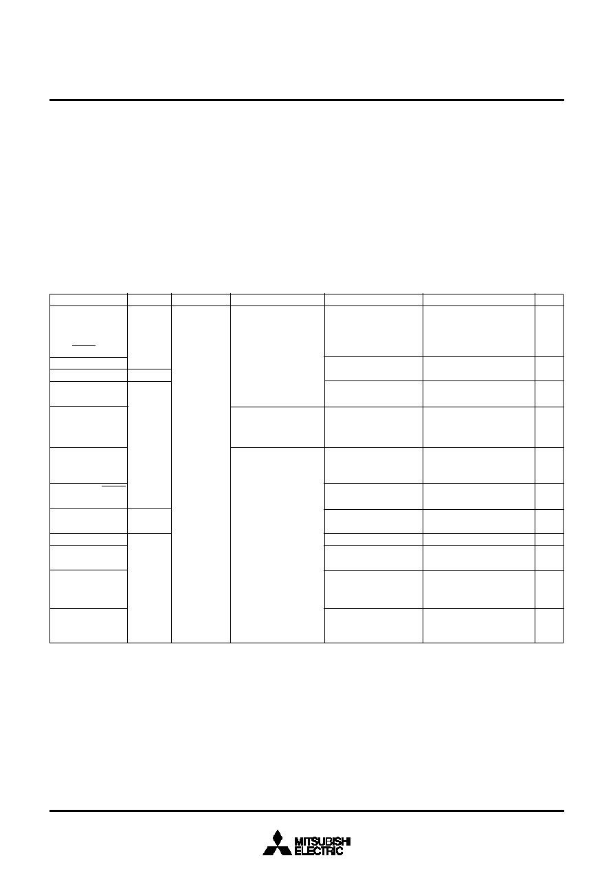
3850 Group (Spec. H)
18
SINGLE-CHIP 8-BIT CMOS MICROCOMPUTER
MITSUBISHI MICROCOMPUTERS
I/O PORTS
The I/O ports have direction registers which determine the input/
output direction of each individual pin. Each bit in a direction
register corresponds to one pin, and each pin can be set to be
input port or output port.
When "0" is written to the bit corresponding to a pin, that pin
becomes an input pin. When "1" is written to that bit, that pin
becomes an output pin.
If data is read from a pin which is set to output, the value of the
port output latch is read, not the value of the pin itself. Pins set to
input are floating. If a pin set to input is written to, only the port
output latch is written to and the pin remains floating.
Pin
Name
Input/Output
I/O Structure
Non-Port Function
Table 9 I/O port function (spec. A)
Related SFRs
Port P0
Port P1
Port P2
P0
0
/S
IN2
P0
1
/S
OUT2
P0
2
/S
CLK2
P0
3
/S
RDY2
P0
4
/AN
5
≠P0
7
AN
8
P1
0
≠P1
7
P2
0
/X
COUT
P2
1
/X
CIN
P2
2
P2
3
P2
4
/RxD
P2
5
/TxD
P2
6
/S
CLK
P2
7
/CNTR
0
/S
RDY1
P3
0
/AN
0
≠
P3
4
/AN
4
P4
0
/CNTR
1
P4
1
/INT
0
P4
2
/INT
1
P4
3
/INT
2
/S
CMP2
P4
4
/INT
3
/PWM
CMOS compatible
input level
CMOS 3-state output
Serial I/O2 control register
CMOS compatible
input level
CMOS 3-state output
Input/output,
individual
bits
Ref.No.
(1)
(2)
(3)
(4)
CMOS compatible
input level
N-channel open-drain
output
Port P3
Port P4
(Note)
Note: When bits 5 to 7 of Ports P3 and P4 are read out, the contents are undefined.
3850 Group (Spec. A)
By setting the port P0, P1, P2 pull-up control register (address
0012
16
), the port P3 pull-up control register (address 0013
16
), or
the port P4 pull-up control register (address 0014
16
), ports can
control pull-up with a program. However, the contents of these
registers do not affect ports programmed as the output ports.
Serial I/O2 function I/O
A-D conversion input
Sub-clock generating
circuit
Serial I/O1 function I/O
Serial I/O1 function I/O
Timer X function I/O
A-D conversion input
Timer Y function I/O
External interrupt input
External interrupt input
S
CMP2
output
External interrupt input
PWM output
A-D control register
A-D input selection register
CPU mode register
Serial I/O1 control register
Serial I/O1 control register
Timer XY mode register
A-D control register
A-D input selection register
Timer XY mode register
Interrupt edge selection
register
Interrupt edge selection
register
Serial I/O2 control register
Interrupt edge selection
register
PWM control register
(13)
(5)
(6)
(7)
(8)
(9)
(10)
(11)
(12)
(13)
(14)
(15)
(16)
(17)

19
SINGLE-CHIP 8-BIT CMOS MICROCOMPUTER
MITSUBISHI MICROCOMPUTERS
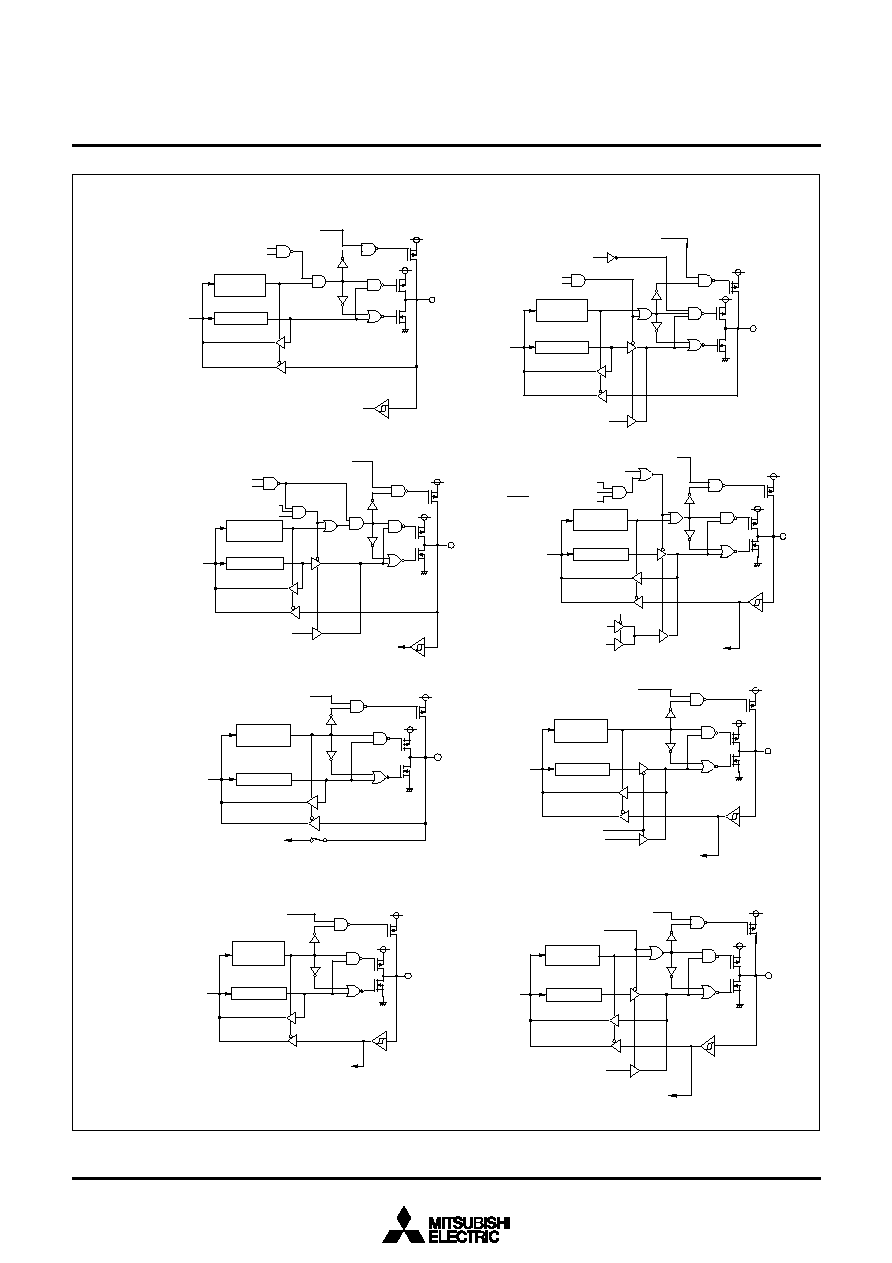
Fig. 13 Port block diagram (1) (spec. H)
3850 Group (Spec. H)
Port latch
(1) Port P0
0
(2) Port P0
1
P0
1
/S
OUT2
P-channel output disable bit
P0
2
/S
CLK2
P-channel output disable bit
Direction
register
Port latch
Direction
register
Port latch
Direction
register
Port latch
Direction
register
Port latch
Direction
register
Direction
register
Port latch
Direction
register
Port latch
Direction
register
Port latch
Data bus
Data bus
Data bus
Data bus
Data bus
Data bus
Serial I/O2 input
Serial I/O2 output
Serial I/O2 Transmit completion signal
Serial I/O2 port selection bit
(3) Port P0
2
Serial I/O2 synchronous
clock selection bit
Serial I/O2 port selection bit
Serial I/O2 clock output
Serial I/O2 external clock input
(4) Port P0
3
Serial I/O2 ready output
S
RDY2
output enable bit
(5) Ports P0
4
-P0
7,
P1
(6) Port P2
0
Port X
C
switch bit
Oscillator
Port X
C
switch bit
Port P2
1
(7) Port P2
1
Port X
C
switch bit
Data bus
Sub-clock generating circuit input
(8) Ports P2
2,
P2
3
Data bus
20
SINGLE-CHIP 8-BIT CMOS MICROCOMPUTER
MITSUBISHI MICROCOMPUTERS
Fig. 14 Port block diagram (2) (spec. H)
3850 Group (Spec. H)
Port latch
Direction
register
Data bus
(9) Port P2
4
Port latch
Direction
register
Data bus
Port latch
Direction
register
Data bus
Port latch
Direction
register
Data bus
Port latch
Direction
register
Data bus
Port latch
Direction
register
Data bus
Port latch
Direction
register
Data bus
Port latch
Direction
register
Data bus
Serial I/O1 enable bit
Receive enable bit
Serial I/O1 input
(11) Port P2
6
Serial I/O1 synchronous
clock selection bit
Serial I/O1 enable bit
Serial I/O1 enable bit
Serial I/O1 mode selection bit
Serial I/O1 clock output
External clock input
(13) Ports P3
0
-P3
4
A-D converter input
Analog input pin selection bit
(15) Ports P4
1
,P4
2
Interrupt input
(10) Port P2
5
P-channel output disable bit
Serial I/O1 enable bit
Transmit enable bit
Serial I/O1 output
(12) Port P2
7
Serial I/O1 enable bit
Serial I/O1 mode selection bit
Pulse output mode
S
RDY1
output enable bit
Timer output
CNTR
0
interrupt
input
Serial ready output
Pulse output mode
(14) Port P4
0
Timer output
CNTR
1
interrupt
input
Pulse output mode
(16) Port P4
3
Interrupt input
Serial I/O2 I/O
comparison signal control bit
Serial I/O2 I/O
comparison signal output

21
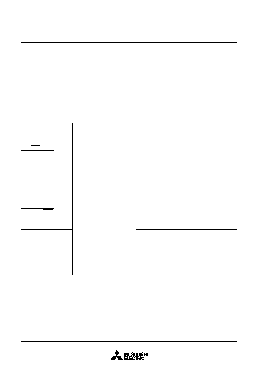
SINGLE-CHIP 8-BIT CMOS MICROCOMPUTER
MITSUBISHI MICROCOMPUTERS
Fig. 15 Port block diagram (3) (spec. H)
3850 Group (Spec. H)
(17) Port P4
4
PWM output
Data bus
PWM output enable bit
Interrupt input
Port latch
Direction
register
22
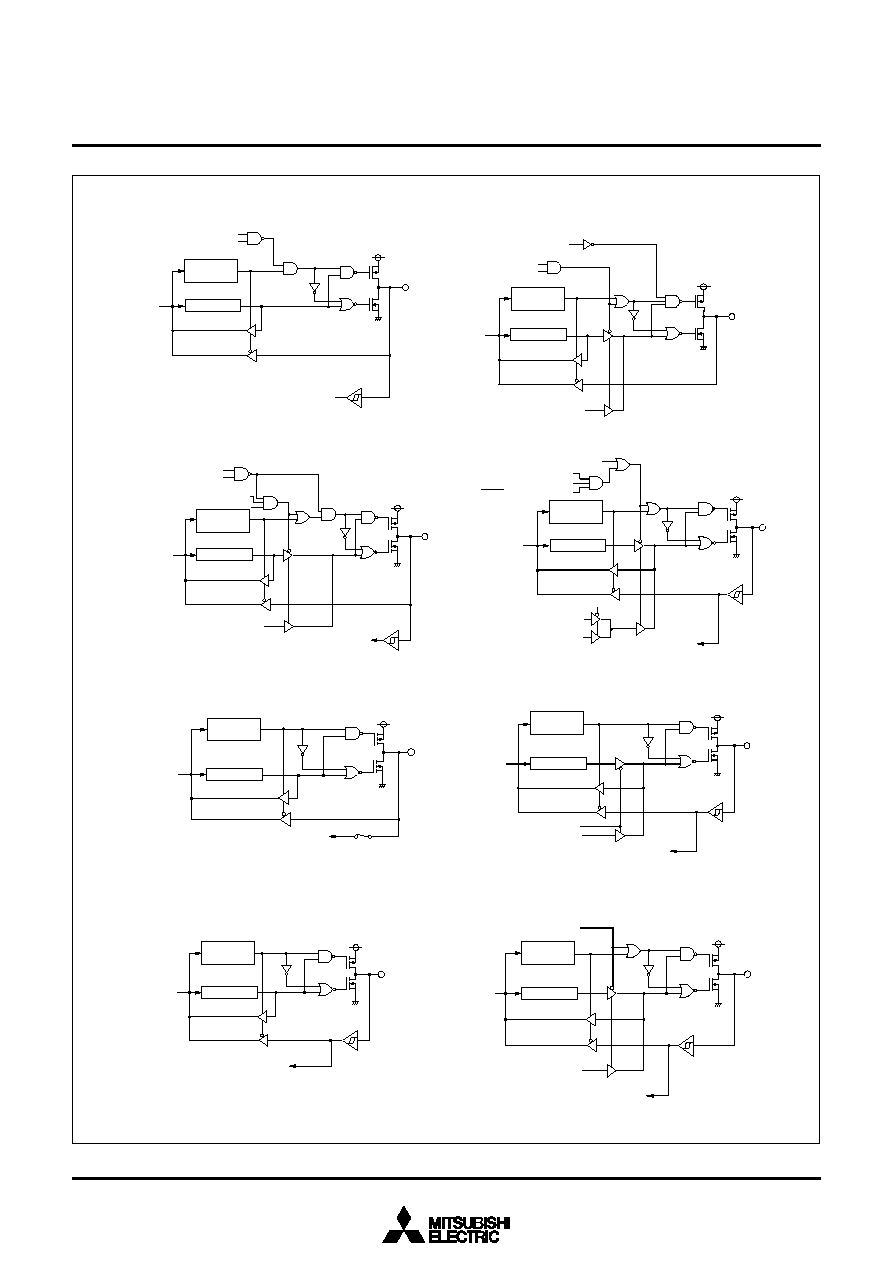
SINGLE-CHIP 8-BIT CMOS MICROCOMPUTER
MITSUBISHI MICROCOMPUTERS
Fig. 16 Port block diagram (1) (spec. A)
3850 Group (Spec. A)
(1) Port P0
0
Port latch
Direction
register
Data bus
Serial I/O2 input
Pull-up control bit
(3) Port P0
2
Pull-up control bit
P0
2
/S
CLK2
P-channel output disable bit
Serial I/O2 synchronous
clock selection bit
Serial I/O2 port selection bit
Port latch
Direction
register
Data bus
Serial I/O2 clock output
Serial I/O2 external clock input
(5) Port P1
Pull-up control bit
Direction
register
Port latch
Data bus
(7) Port P2
1
Pull-up control bit
Port X
C
switch bit
Data bus
Direction
register
Port latch
Sub-clock generating circuit input
(2) Port P0
1
P0
1
/S
OUT2
P-channel output disable bit
Serial I/O2 Transmit completion signal
Serial I/O2 port selection bit
Direction
register
Data bus
Port latch
Serial I/O2 output
Pull-up control bit
(4) Port P0
3
Pull-up control bit
S
RDY2
output enable bit
Direction
register
Port latch
Data bus
Serial I/O2 ready output
(6) Port P2
0
Port X
C
switch bit
Pull-up control bit
Oscillator
Port X
C
switch bit
Port P2
1
Direction
register
Data bus
Port latch
(8) Ports P2
2,
P2
3
Data bus
Direction
register
Port latch
23
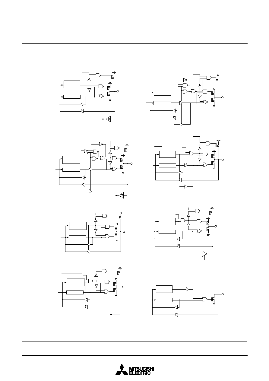
SINGLE-CHIP 8-BIT CMOS MICROCOMPUTER
MITSUBISHI MICROCOMPUTERS
Fig. 17 Port block diagram (2) (spec. A)
3850 Group (Spec. A)
(
9
)
P
o
r
t
P
2
4
P
o
r
t
l
a
t
c
h
Direction
register
D
a
t
a
b
u
s
Serial I/O1 enable bit
R
e
c
e
i
v
e
e
n
a
b
l
e
b
i
t
Pull-up control bit
S
e
r
i
a
l
I
/
O
1
i
n
p
u
t
(
1
1
)
P
o
r
t
P
2
6
P
u
l
l
-
u
p
c
o
n
t
r
o
l
b
i
t
S
e
r
i
a
l
I
/
O
1
s
y
n
c
h
r
o
n
o
u
s
c
l
o
c
k
s
e
l
e
c
t
i
o
n
b
i
t
Serial I/O1 enable bit
S
e
r
i
a
l
I
/
O
1
e
n
a
b
l
e
b
i
t
S
e
r
i
a
l
I
/
O
1
m
o
d
e
s
e
l
e
c
t
i
o
n
b
i
t
Port latch
D
i
r
e
c
t
i
o
n
r
e
g
i
s
t
e
r
D
a
t
a
b
u
s
S
e
r
i
a
l
I
/
O
1
c
l
o
c
k
o
u
t
p
u
t
E
x
t
e
r
n
a
l
c
l
o
c
k
i
n
p
u
t
(
1
3
)
P
o
r
t
s
P
0
4
-
P
0
7
,
P
3
0
-
P
3
4
P
u
l
l
-
u
p
c
o
n
t
r
o
l
b
i
t
Direction
register
P
o
r
t
l
a
t
c
h
Data bus
A
-
D
c
o
n
v
e
r
t
e
r
i
n
p
u
t
A
n
a
l
o
g
i
n
p
u
t
p
i
n
s
e
l
e
c
t
i
o
n
b
i
t
A
n
a
l
o
g
i
n
p
u
t
p
o
r
t
s
e
l
e
c
t
i
o
n
s
w
i
t
c
h
b
i
t
(
1
5
)
P
o
r
t
s
P
4
1
,
P
4
2
I
n
t
e
r
r
u
p
t
i
n
p
u
t
P
u
l
l
-
u
p
c
o
n
t
r
o
l
b
i
t
D
i
r
e
c
t
i
o
n
r
e
g
i
s
t
e
r
Port latch
Data bus
(10) Port P2
5
P-channel output disable bit
S
e
r
i
a
l
I
/
O
1
e
n
a
b
l
e
b
i
t
Transmit enable bit
Pull-up control bit
S
e
r
i
a
l
I
/
O
1
o
u
t
p
u
t
P
o
r
t
l
a
t
c
h
Direction
register
Data bus
(
1
2
)
P
o
r
t
P
2
7
Serial I/O1 enable bit
Serial I/O1 mode selection bit
S
R
D
Y
1
o
u
t
p
u
t
e
n
a
b
l
e
b
i
t
P
u
l
s
e
o
u
t
p
u
t
m
o
d
e
P
u
l
l
-
u
p
c
o
n
t
r
o
l
b
i
t
Port latch
D
i
r
e
c
t
i
o
n
r
e
g
i
s
t
e
r
Data bus
Pulse output mode
Timer output
Serial ready output
CNTR
0
interrupt
input
Pull-up control bit
(14) Port P4
0
Data bus
Direction
register
Port latch
T
i
m
e
r
o
u
t
p
u
t
P
u
l
s
e
o
u
t
p
u
t
m
o
d
e
CNTR
1
interrupt
input
(16) Port P4
3
P
u
l
l
-
u
p
c
o
n
t
r
o
l
b
i
t
Serial I/O2 I/O
comparison signal control bit
Direction
register
P
o
r
t
l
a
t
c
h
D
a
t
a
b
u
s
Interrupt input
Serial I/O2 I/O
comparison signal output
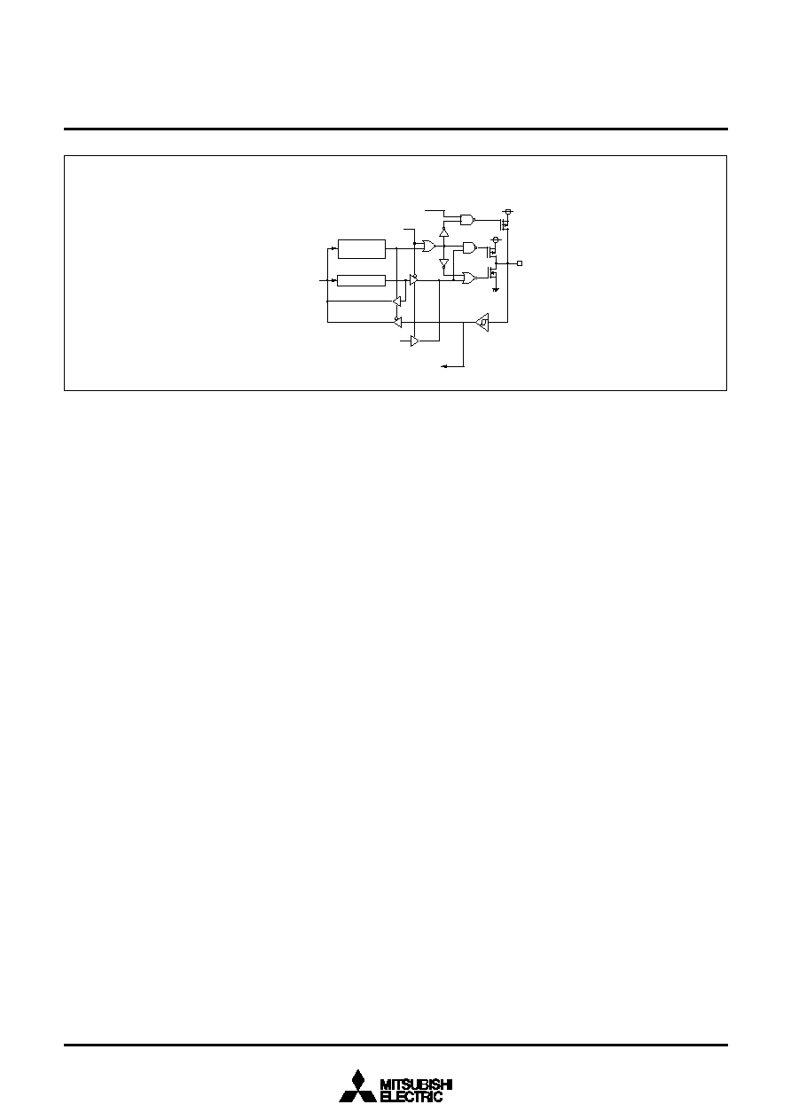
24
SINGLE-CHIP 8-BIT CMOS MICROCOMPUTER
MITSUBISHI MICROCOMPUTERS
Fig. 18 Port block diagram (3) (spec. A)
3850 Group (Spec. A)
(17) Port P4
4
PWM output
D
a
t
a
b
u
s
P
W
M
o
u
t
p
u
t
e
n
a
b
l
e
b
i
t
I
n
t
e
r
r
u
p
t
i
n
p
u
t
Port latch
D
i
r
e
c
t
i
o
n
r
e
g
i
s
t
e
r
P
u
l
l
-
u
p
c
o
n
t
r
o
l
b
i
t
25
SINGLE-CHIP 8-BIT CMOS MICROCOMPUTER
MITSUBISHI MICROCOMPUTERS
Fig. 19 Structure of port registers (1) (spec. A)
3850 Group (Spec. A)
Port P0, P1, P2 pull-up control register
b7
b0
P0 pull-up control bit
0: No pull-up
1: Pull-up
P1 pull-up control bit
0: No pull-up
1: Pull-up
P2 pull-up control bit
0: No pull-up
1: Pull-up
Not used (return "0" when read)
b
7
b
0
Port P3 pull-up control register
P3
0
pull-up control bit
0: No pull-up
1: Pull-up
P3
1
pull-up control bit
0: No pull-up
1: Pull-up
P3
2
pull-up control bit
0: No pull-up
1: Pull-up
P3
3
pull-up control bit
0: No pull-up
1: Pull-up
P3
4
pull-up control bit
0: No pull-up
1: Pull-up
Fix these bits to "0".
(PULL3: address 0013
16
)
(PULL012: address 0012
16
)
Note: Pull-up control is valid when the corresponding bit
of the port direction register is "0" (input).
When that bit is "1" (output), pull-up cannot be set
to the port of which pull-up is selected.
Note: Pull-up control is valid when the corresponding bit
of the port direction register is "0" (input).
When that bit is "1" (output), pull-up cannot be set
to the port of which pull-up is selected.
26
SINGLE-CHIP 8-BIT CMOS MICROCOMPUTER
MITSUBISHI MICROCOMPUTERS
Fig. 20 Structure of port registers (2) (spec. A)
3850 Group (Spec. A)
b
7
b
0
P
o
r
t
P
4
p
u
l
l
-
u
p
c
o
n
t
r
o
l
r
e
g
i
s
t
e
r
P4
0
pull-up control bit
0: No pull-up
1: Pull-up
P4
1
pull-up control bit
0: No pull-up
1: Pull-up
P4
2
pull-up control bit
0: No pull-up
1: Pull-up
P4
3
pull-up control bit
0: No pull-up
1: Pull-up
P4
4
pull-up control bit
0: No pull-up
1: Pull-up
Fix these bits to "0".
(
P
U
L
L
4
:
a
d
d
r
e
s
s
0
0
1
4
1
6
)
Note: Pull-up control is valid when the corresponding bit
of the port direction register is "0" (input).
When that bit is "1" (output), pull-up cannot be set
to the port of which pull-up is selected.

27
SINGLE-CHIP 8-BIT CMOS MICROCOMPUTER
MITSUBISHI MICROCOMPUTERS
3850 Group (Spec. H/A)
INTERRUPTS
Interrupts occur by 15 sources among 15 sources: six external,
eight internal, and one software.
Interrupt Control
Each interrupt is controlled by an interrupt request bit, an interrupt
enable bit, and the interrupt disable flag except for the software in-
terrupt set by the BRK instruction. An interrupt occurs if the
corresponding interrupt request and enable bits are "1" and the in-
terrupt disable flag is "0".
Interrupt enable bits can be set or cleared by software.
Interrupt request bits can be cleared by software, but cannot be
set by software.
The BRK instruction cannot be disabled with any flag or bit. The I
(interrupt disable) flag disables all interrupts except the BRK in-
struction interrupt.
When several interrupts occur at the same time, the interrupts are
received according to priority.
Interrupt Operation
By acceptance of an interrupt, the following operations are auto-
matically performed:
1. The contents of the program counter and the processor status
register are automatically pushed onto the stack.
2. The interrupt disable flag is set and the corresponding interrupt
request bit is cleared.
3. The interrupt jump destination address is read from the vector
table into the program counter.
s
Notes
When setting the followings, the interrupt request bit may be set to
"1".
∑When setting external interrupt active edge
Related register: Interrupt edge selection register (address 3A
16
)
Timer XY mode register (address 23
16
)
∑When switching interrupt sources of an interrupt vector address
where two or more interrupt sources are allocated
Related register: Interrupt edge selection register (address 3A
16
)
When not requiring for the interrupt occurrence synchronized with
these setting, take the following sequence.
Set the corresponding interrupt enable bit to "0" (disabled).
Set the interrupt edge select bit or the interrupt source select bit
to "1".
Set the corresponding interrupt request bit to "0" after 1 or more
instructions have been executed.
Set the corresponding interrupt enable bit to "1" (enabled).
28
SINGLE-CHIP 8-BIT CMOS MICROCOMPUTER
MITSUBISHI MICROCOMPUTERS
3850 Group (Spec. H/A)
Interrupt Request
Generating Conditions
Remarks
Interrupt Source
Low
FFFC
16
High
FFFD
16
Priority
1
Table 10 Interrupt vector addresses and priority
Notes 1: Vector addresses contain interrupt jump destination addresses.
2: Reset function in the same way as an interrupt with the highest priority.
Vector Addresses (Note 1)
Reset (Note 2)
INT
0
Reserved
INT
1
INT
2
INT
3
/ Serial I/O2
Reserved
Timer X
Timer Y
Timer 1
Timer 2
Serial I/O1
reception
Serial I/O1
transmission
CNTR
0
CNTR
1
A-D converter
BRK instruction
At reset
At detection of either rising or
falling edge of INT
0
input
At detection of either rising or
falling edge of INT
1
input
At detection of either rising or
falling edge of INT
2
input
At detection of either rising or
falling edge of INT
3
input/ At
completion of serial I/O2 data
reception/transmission
Reserved
At completion of serial I/O1 data
reception
At completion of serial I/O1
transfer shift or when transmis-
sion buffer is empty
At timer X underflow
At timer Y underflow
At timer 1 underflow
At timer 2 underflow
Non-maskable
External interrupt
(active edge selectable)
Valid when serial I/O1 is selected
Valid when serial I/O1 is selected
External interrupt
(active edge selectable)
STP release timer underflow
External interrupt
(active edge selectable)
Reserved
At detection of either rising or
falling edge of CNTR
0
input
At detection of either rising or
falling edge of CNTR
1
input
At completion of A-D conversion
At BRK instruction execution
External interrupt
(active edge selectable)
External interrupt
(active edge selectable)
External interrupt
(active edge selectable)
Switch by Serial I/O2/INT
3
interrupt source bit
FFFA
16
FFF8
16
FFF6
16
FFF4
16
FFF2
16
FFF0
16
FFEE
16
FFEC
16
FFEA
16
FFE8
16
FFE6
16
FFE4
16
FFE2
16
FFE0
16
FFDE
16
FFFB
16
FFF9
16
FFF7
16
FFF5
16
FFF3
16
FFF1
16
FFEF
16
FFED
16
FFEB
16
FFE9
16
FFE7
16
FFE5
16
FFE3
16
FFE1
16
FFDF
16
FFDC
16
FFDD
16
2
3
4
5
6
7
8
9
10
11
12
13
14
15
16
17
Non-maskable software interrupt
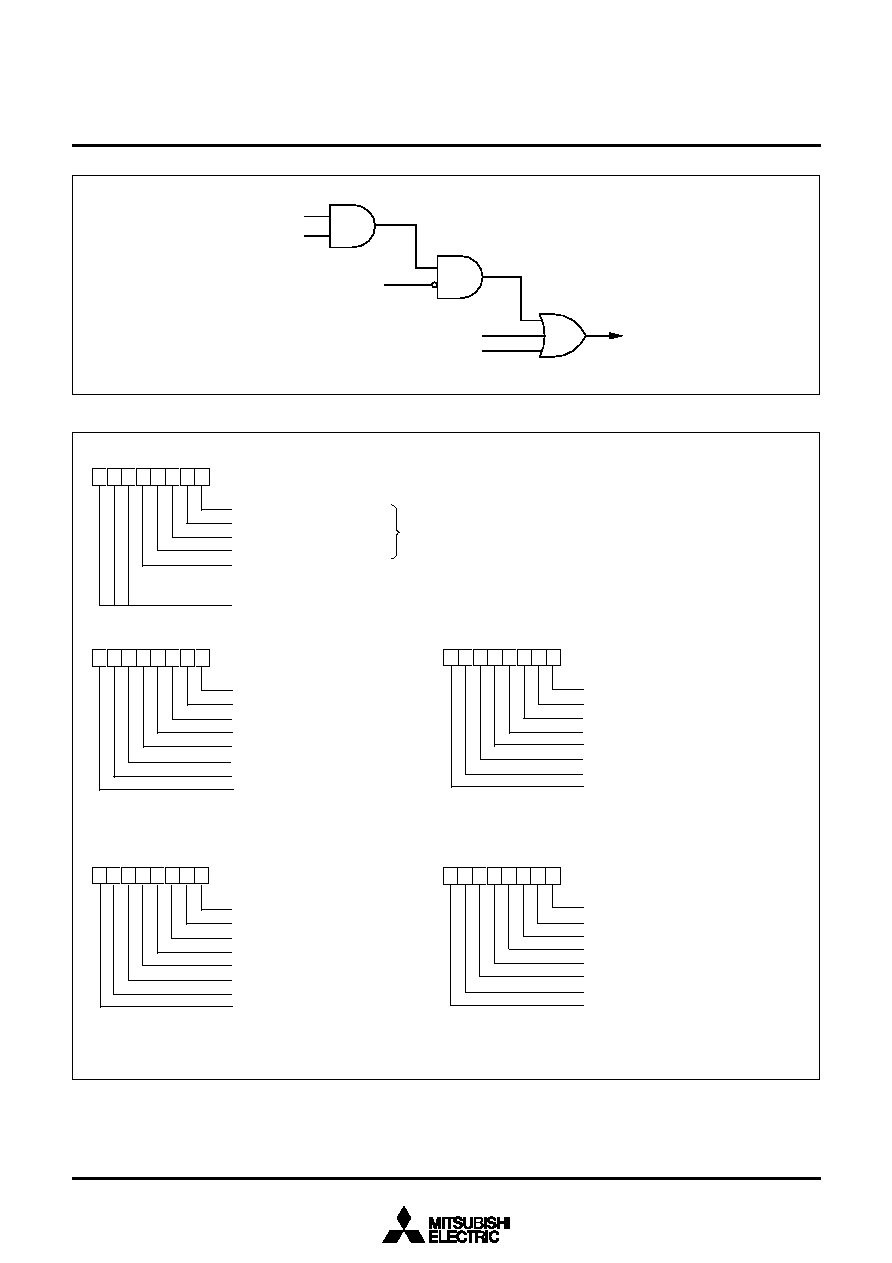
29
SINGLE-CHIP 8-BIT CMOS MICROCOMPUTER
MITSUBISHI MICROCOMPUTERS
Fig. 21 Interrupt control
Fig. 22 Structure of interrupt-related registers
3850 Group (Spec. H/A)
Interrupt disable flag (I)
Interrupt request
Interrupt request bit
Interrupt enable bit
BRK instruction
Reset
b7 b0
b7 b0
b
7
b
0
b7 b0
b7 b0
I
n
t
e
r
r
u
p
t
e
d
g
e
s
e
l
e
c
t
i
o
n
r
e
g
i
s
t
e
r
I
N
T
0
a
c
t
i
v
e
e
d
g
e
s
e
l
e
c
t
i
o
n
b
i
t
I
N
T
1
a
c
t
i
v
e
e
d
g
e
s
e
l
e
c
t
i
o
n
b
i
t
I
N
T
2
a
c
t
i
v
e
e
d
g
e
s
e
l
e
c
t
i
o
n
b
i
t
I
N
T
3
a
c
t
i
v
e
e
d
g
e
s
e
l
e
c
t
i
o
n
b
i
t
S
e
r
i
a
l
I
/
O
2
/
I
N
T
3
i
n
t
e
r
r
u
p
t
s
o
u
r
c
e
b
i
t
0
:
I
N
T
3
i
n
t
e
r
r
u
p
t
s
e
l
e
c
t
e
d
1
:
S
e
r
i
a
l
I
/
O
2
i
n
t
e
r
r
u
p
t
s
e
l
e
c
t
e
d
N
o
t
u
s
e
d
(
r
e
t
u
r
n
s
"
0
"
w
h
e
n
r
e
a
d
)
(INTEDGE : address 003A
16
)
0
:
F
a
l
l
i
n
g
e
d
g
e
a
c
t
i
v
e
1
:
R
i
s
i
n
g
e
d
g
e
a
c
t
i
v
e
Interrupt request register 1
INT
0
interrupt request bit
Reserved
INT
1
interrupt request bit
INT
2
interrupt request bit
INT
3
/ Serial I/O2 interrupt request bit
Reserved
Timer X interrupt request bit
Timer Y interrupt request bit
0 : No interrupt request issued
1 : Interrupt request issued
(IREQ1 : address 003C
16
)
Interrupt request register 2
T
i
m
e
r
1
i
n
t
e
r
r
u
p
t
r
e
q
u
e
s
t
b
i
t
T
i
m
e
r
2
i
n
t
e
r
r
u
p
t
r
e
q
u
e
s
t
b
i
t
S
e
r
i
a
l
I
/
O
1
r
e
c
e
p
t
i
o
n
i
n
t
e
r
r
u
p
t
r
e
q
u
e
s
t
b
i
t
S
e
r
i
a
l
I
/
O
1
t
r
a
n
s
m
i
t
i
n
t
e
r
r
u
p
t
r
e
q
u
e
s
t
b
i
t
C
N
T
R
0
i
n
t
e
r
r
u
p
t
r
e
q
u
e
s
t
b
i
t
C
N
T
R
1
i
n
t
e
r
r
u
p
t
r
e
q
u
e
s
t
b
i
t
A
D
c
o
n
v
e
r
t
e
r
i
n
t
e
r
r
u
p
t
r
e
q
u
e
s
t
b
i
t
N
o
t
u
s
e
d
(
r
e
t
u
r
n
s
"
0
"
w
h
e
n
r
e
a
d
)
(IREQ2 : address 003D
16
)
0 : No interrupt request issued
1 : Interrupt request issued
I
n
t
e
r
r
u
p
t
c
o
n
t
r
o
l
r
e
g
i
s
t
e
r
1
I
N
T
0
i
n
t
e
r
r
u
p
t
e
n
a
b
l
e
b
i
t
R
e
s
e
r
v
e
d
(
D
o
n
o
t
w
r
i
t
e
"
1
"
t
o
t
h
i
s
b
i
t
.
)
I
N
T
1
i
n
t
e
r
r
u
p
t
e
n
a
b
l
e
b
i
t
I
N
T
2
i
n
t
e
r
r
u
p
t
e
n
a
b
l
e
b
i
t
I
N
T
3
/
S
e
r
i
a
l
I
/
O
2
i
n
t
e
r
r
u
p
t
e
n
a
b
l
e
b
i
t
R
e
s
e
r
v
e
d
(
D
o
n
o
t
w
r
i
t
e
"
1
"
t
o
t
h
i
s
b
i
t
.
)
T
i
m
e
r
X
i
n
t
e
r
r
u
p
t
e
n
a
b
l
e
b
i
t
T
i
m
e
r
Y
i
n
t
e
r
r
u
p
t
e
n
a
b
l
e
b
i
t
(
I
C
O
N
1
:
a
d
d
r
e
s
s
0
0
3
E
1
6
)
I
n
t
e
r
r
u
p
t
c
o
n
t
r
o
l
r
e
g
i
s
t
e
r
2
Timer 1 interrupt enable bit
Timer 2 interrupt enable bit
Serial I/O1 reception interrupt enable bit
Serial I/O1 transmit interrupt enable bit
CNTR
0
interrupt enable bit
CNTR
1
interrupt enable bit
AD converter interrupt enable bit
Not used (returns "0" when read)
(Do not write "1" to this bit.)
0
:
I
n
t
e
r
r
u
p
t
s
d
i
s
a
b
l
e
d
1
:
I
n
t
e
r
r
u
p
t
s
e
n
a
b
l
e
d
(
I
C
O
N
2
:
a
d
d
r
e
s
s
0
0
3
F
1
6
)
0
:
I
n
t
e
r
r
u
p
t
s
d
i
s
a
b
l
e
d
1
:
I
n
t
e
r
r
u
p
t
s
e
n
a
b
l
e
d
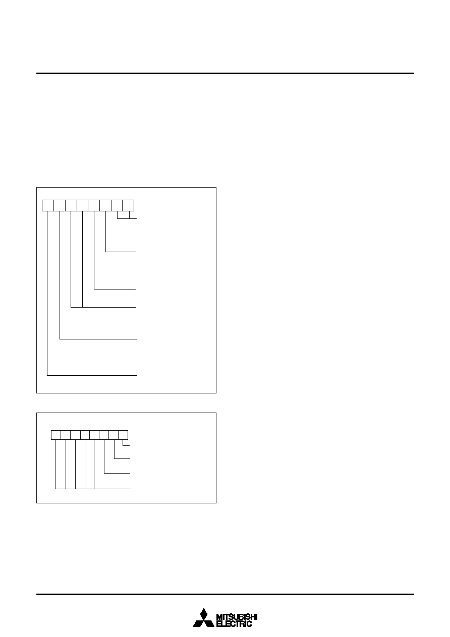
30
SINGLE-CHIP 8-BIT CMOS MICROCOMPUTER
MITSUBISHI MICROCOMPUTERS
TIMERS
The 3850 group (spec. H/A) has four timers: timer X, timer Y, timer
1, and timer 2.
The division ratio of each timer or prescaler is given by 1/(n + 1),
where n is the value in the corresponding timer or prescaler latch.
All timers are count down. When the timer reaches "00
16
", an un-
derflow occurs at the next count pulse and the corresponding
timer latch is reloaded into the timer and the count is continued.
When a timer underflows, the interrupt request bit corresponding
to that timer is set to "1".
Timer X and Timer Y
Timer X and Timer Y can each select in one of four operating
modes by setting the timer XY mode register.
(1) Timer Mode
The timer counts the count source selected by Timer count source
selection bit.
(2) Pulse Output Mode
The timer counts the count source selected by Timer count source
selection bit. Whenever the contents of the timer reach "00
16
", the
signal output from the CNTR
0
(or CNTR
1
) pin is inverted. If the
CNTR
0
(or CNTR
1
) active edge selection bit is "0", output begins
at " H".
If it is "1", output starts at "L". When using a timer in this mode, set
the corresponding port P2
7
( or port P4
0
) direction register to out-
put mode.
(3) Event Counter Mode
Operation in event counter mode is the same as in timer mode,
except that the timer counts signals input through the CNTR
0
or
CNTR
1
pin.
When the CNTR
0
(or CNTR
1
) active edge selection bit is "0", the
rising edge of the CNTR
0
(or CNTR
1
) pin is counted.
When the CNTR
0
(or CNTR
1
) active edge selection bit is "1", the
falling edge of the CNTR
0
(or CNTR
1
) pin is counted.
(4) Pulse Width Measurement Mode
If the CNTR
0
(or CNTR
1
) active edge selection bit is "0", the timer
counts the selected signals by the count source selection bit while
the CNTR
0
(or CNTR
1
) pin is at "H". If the CNTR
0
(or CNTR
1
) ac-
tive edge selection bit is "1", the timer counts it while the CNTR
0
(or CNTR
1
) pin is at "L".
The count can be stopped by setting "1" to the timer X (or timer Y)
count stop bit in any mode. The corresponding interrupt request
bit is set each time a timer underflows.
Fig. 23 Structure of timer XY mode register
s
Note
When switching the count source by the timer 12, X and Y count
source bits, the value of timer count is altered in unconsiderable
amount owing to generating of a thin pulses in the count input
signals.
Therefore, select the timer count source before set the value to
the prescaler and the timer.
When timer X/timer Y underflow while executing the instruction
which sets "1" to the timer X/timer Y count stop bits, the timer X/
timer Y interrupt request bits are set to "1". Timer X/Timer Y in-
terrupts are received if these interrupts are enabled at this time.
The timing which interrupt is accepted has a case after the in-
struction which sets "1" to the count stop bit, and a case after
the next instruction according to the timing of the timer under-
flow. When this interrupt is unnecessary, set "0" (disabled) to the
interrupt enable bit and then set "1" to the count stop bit.
Fig. 24 Structure of timer count source selection register
3850 Group (Spec. H/A)
Timer 1 and Timer 2
The count source of prescaler 12 is the oscillation frequency
which is selected by timer 12 count source selection bit. The out-
put of prescaler 12 is counted by timer 1 and timer 2, and a timer
underflow sets the interrupt request bit.
T
i
m
e
r
X
c
o
u
n
t
s
t
o
p
b
i
t
0
:
C
o
u
n
t
s
t
a
r
t
1
:
C
o
u
n
t
s
t
o
p
Timer XY mode register
(TM : address 0023
16
)
Timer Y operating mode bits
0 0: Timer mode
0 1: Pulse output mode
1 0: Event counter mode
1 1: Pulse width measurement mode
C
N
T
R
1
a
c
t
i
v
e
e
d
g
e
s
e
l
e
c
t
i
o
n
b
i
t
0
:
I
n
t
e
r
r
u
p
t
a
t
f
a
l
l
i
n
g
e
d
g
e
C
o
u
n
t
a
t
r
i
s
i
n
g
e
d
g
e
i
n
e
v
e
n
t
c
o
u
n
t
e
r
m
o
d
e
1
:
I
n
t
e
r
r
u
p
t
a
t
r
i
s
i
n
g
e
d
g
e
C
o
u
n
t
a
t
f
a
l
l
i
n
g
e
d
g
e
i
n
e
v
e
n
t
c
o
u
n
t
e
r
m
o
d
e
b
7
CNTR
0
active edge selection bit
0: Interrupt at falling edge
Count at rising edge in event
counter mode
1: Interrupt at rising edge
Count at falling edge in event
counter mode
b
0
T
i
m
e
r
X
o
p
e
r
a
t
i
n
g
m
o
d
e
b
i
t
0
0
:
T
i
m
e
r
m
o
d
e
0
1
:
P
u
l
s
e
o
u
t
p
u
t
m
o
d
e
1
0
:
E
v
e
n
t
c
o
u
n
t
e
r
m
o
d
e
1
1
:
P
u
l
s
e
w
i
d
t
h
m
e
a
s
u
r
e
m
e
n
t
m
o
d
e
b1b0
b5b4
Timer Y count stop bit
0: Count start
1: Count stop
T
i
m
e
r
c
o
u
n
t
s
o
u
r
c
e
s
e
l
e
c
t
i
o
n
r
e
g
i
s
t
e
r
(
T
C
S
S
:
a
d
d
r
e
s
s
0
0
2
8
1
6
)
b
7
b
0
T
i
m
e
r
X
c
o
u
n
t
s
o
u
r
c
e
s
e
l
e
c
t
i
o
n
b
i
t
0
:
f
(
X
I
N
)
/
1
6
(
f
(
X
C
I
N
)
/
1
6
a
t
l
o
w
-
s
p
e
e
d
m
o
d
e
)
1
:
f
(
X
I
N
)
/
2
(
f
(
X
C
I
N
)
/
2
a
t
l
o
w
-
s
p
e
e
d
m
o
d
e
)
T
i
m
e
r
Y
c
o
u
n
t
s
o
u
r
c
e
s
e
l
e
c
t
i
o
n
b
i
t
0
:
f
(
X
I
N
)
/
1
6
(
f
(
X
C
I
N
)
/
1
6
a
t
l
o
w
-
s
p
e
e
d
m
o
d
e
)
1
:
f
(
X
I
N
)
/
2
(
f
(
X
C
I
N
)
/
2
a
t
l
o
w
-
s
p
e
e
d
m
o
d
e
)
Timer 12 count source selection bit
0 : f(X
IN
)/16 (f(X
CIN
)/16 at low-speed mode)
1 : f(X
CIN
)
N
o
t
u
s
e
d
(
r
e
t
u
r
n
s
"
0
"
w
h
e
n
r
e
a
d
)

31
SINGLE-CHIP 8-BIT CMOS MICROCOMPUTER
MITSUBISHI MICROCOMPUTERS
3850 Group (Spec. H/A)
Fig. 25 Block diagram of timer X, timer Y, timer 1, and timer 2
Q
Q
"1"
"0"
P
2
7
/
C
N
T
R
0
Q
Q
P
4
0
/
C
N
T
R
1
"
0
"
"1"
R
R
"
1
"
"
0
"
"0"
"1"
T
T
P
r
e
s
c
a
l
e
r
X
l
a
t
c
h
(
8
)
P
r
e
s
c
a
l
e
r
X
(
8
)
T
i
m
e
r
X
l
a
t
c
h
(
8
)
T
i
m
e
r
X
(
8
)
T
o
t
i
m
e
r
X
i
n
t
e
r
r
u
p
t
r
e
q
u
e
s
t
b
i
t
Toggle flip-flop
Timer X count stop bit
P
u
l
s
e
w
i
d
t
h
m
e
a
s
u
r
e
m
e
n
t
m
o
d
e
Event
counter
mode
T
o
C
N
T
R
0
i
n
t
e
r
r
u
p
t
r
e
q
u
e
s
t
b
i
t
P
u
l
s
e
o
u
t
p
u
t
m
o
d
e
P
o
r
t
P
2
7
l
a
t
c
h
Port P2
7
direction register
C
N
T
R
0
a
c
t
i
v
e
e
d
g
e
s
e
l
e
c
t
i
o
n
b
i
t
T
i
m
e
r
X
l
a
t
c
h
w
r
i
t
e
p
u
l
s
e
P
u
l
s
e
o
u
t
p
u
t
m
o
d
e
T
i
m
e
r
m
o
d
e
P
u
l
s
e
o
u
t
p
u
t
m
o
d
e
Prescaler Y latch (8)
Prescaler Y (8)
T
i
m
e
r
Y
l
a
t
c
h
(
8
)
Timer Y (8)
T
o
t
i
m
e
r
Y
i
n
t
e
r
r
u
p
t
r
e
q
u
e
s
t
b
i
t
T
o
g
g
l
e
f
l
i
p
-
f
l
o
p
T
i
m
e
r
Y
c
o
u
n
t
s
t
o
p
b
i
t
To CNTR
1
interrupt
request bit
Pulse output mode
P
o
r
t
P
4
0
l
a
t
c
h
Port P4
0
direction register
CNTR
1
active
edge selection
bit
Timer Y latch write pulse
Pulse output mode
Timer mode
Pulse output mode
D
a
t
a
b
u
s
D
a
t
a
b
u
s
Prescaler 12 latch (8)
P
r
e
s
c
a
l
e
r
1
2
(
8
)
Timer 1 latch (8)
Timer 1 (8)
Data bus
Timer 2 latch (8)
Timer 2 (8)
To timer 2 interrupt
request bit
To timer 1 interrupt
request bit
C
N
T
R
0
a
c
t
i
v
e
e
d
g
e
s
e
l
e
c
t
i
o
n
b
i
t
CNTR
1
active edge
selection bit
Pulse width
measure-
ment mode
E
v
e
n
t
c
o
u
n
t
e
r
m
o
d
e
f
(
X
C
I
N
)
T
i
m
e
r
1
2
c
o
u
n
t
s
o
u
r
c
e
s
e
l
e
c
t
i
o
n
b
i
t
f(X
IN
)/16
f(X
IN
)/2
Timer Y count source selection bit
f(X
IN
)/16
f
(
X
I
N
)
/
2
T
i
m
e
r
X
c
o
u
n
t
s
o
u
r
c
e
s
e
l
e
c
t
i
o
n
b
i
t
f
(
X
I
N
)
/
1
6
(
f
(
X
C
I
N
)
/
1
6
a
t
l
o
w
-
s
p
e
e
d
m
o
d
e
)
(
f
(
X
C
I
N
)
/
2
a
t
l
o
w
-
s
p
e
e
d
m
o
d
e
)
(
f
(
X
C
I
N
)
/
1
6
a
t
l
o
w
-
s
p
e
e
d
m
o
d
e
)
(f(X
CIN
)/2 at low-speed mode)
(
f
(
X
C
I
N
)
/
1
6
a
t
l
o
w
-
s
p
e
e
d
m
o
d
e
)
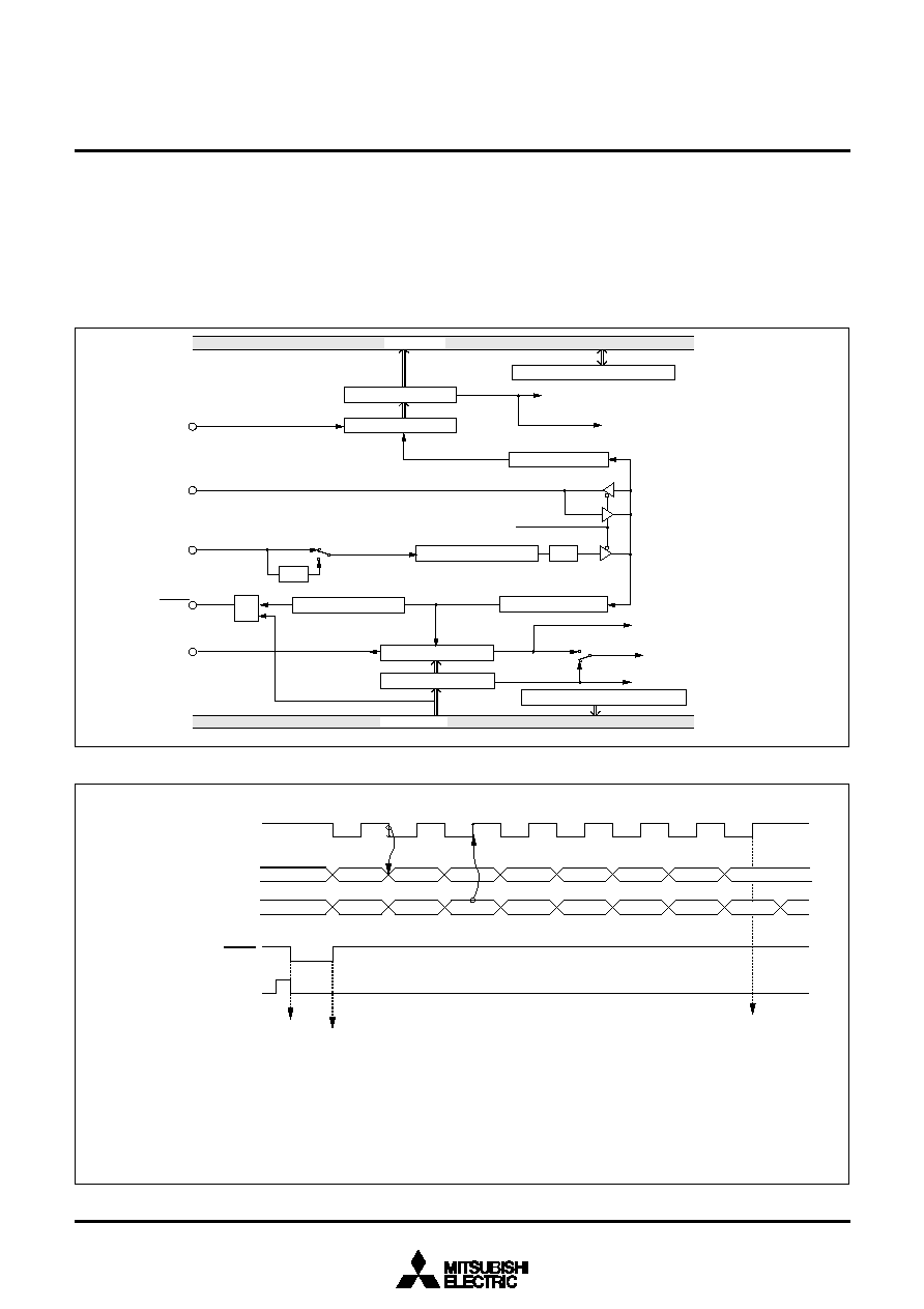
32
SINGLE-CHIP 8-BIT CMOS MICROCOMPUTER
MITSUBISHI MICROCOMPUTERS
SERIAL I/O
q
SERIAL I/O1
Serial I/O1 can be used as either clock synchronous or asynchro-
nous (UART) serial I/O. A dedicated timer is also provided for
baud rate generation.
(1) Clock Synchronous Serial I/O Mode
Clock synchronous serial I/O mode can be selected by setting the
serial I/O1 mode selection bit of the serial I/O1 control register (bit
6 of address 001A
16
) to "1".
For clock synchronous serial I/O, the transmitter and the receiver
must use the same clock. If an internal clock is used, transfer is
started by a write signal to the TB/RB.
Fig. 26 Block diagram of clock synchronous serial I/O1
Fig. 27 Operation of clock synchronous serial I/O1 function
3850 Group (Spec. H/A)
1/4
1/4
F/F
P2
6
/S
CLK
Serial I/O1 status register
Serial I/O1 control register
P2
7
/S
RDY1
P2
4
/R
X
D
P2
5
/T
X
D
X
IN
Receive buffer register
Address 0018
16
Receive shift register
Receive buffer full flag (RBF)
Receive interrupt request (RI)
Clock control circuit
Shift clock
Serial I/O1 synchronous
clock selection bit
Frequency division ratio 1/(n+1)
Baud rate generator
Address 001C
16
BRG count source selection bit
Clock control circuit
Falling-edge detector
Transmit buffer register
Data bus
Address 0018
16
Shift clock
Transmit shift completion flag (TSC)
Transmit buffer empty flag (TBE)
Transmit interrupt request (TI)
Transmit interrupt source selection bit
Address 0019
16
Data bus
Address 001A
16
Transmit shift register
D
7
D
7
D
0
D
1
D
2
D
3
D
4
D
5
D
6
D
0
D
1
D
2
D
3
D
4
D
5
D
6
RBF = 1
TSC = 1
TBE = 0
TBE = 1
TSC = 0
Transfer shift clock
(1/2 to 1/2048 of the internal
clock, or an external clock)
Serial output TxD
Serial input RxD
Write pulse to receive/transmit
buffer register (address 0018
16
)
Overrun error (OE)
detection
Notes 1: As the transmit interrupt (TI), either when the transmit buffer has emptied (TBE=1) or after the transmit shift operation has
ended (TSC=1), by setting the transmit interrupt source selection bit (TIC) of the serial I/O1 control register.
2: If data is written to the transmit buffer register when TSC=0, the transmit clock is generated continuously and serial data
is output continuously from the TxD pin.
3: The receive interrupt (RI) is set when the receive buffer full flag (RBF) becomes "1" .
Receive enable signal
S
RDY1
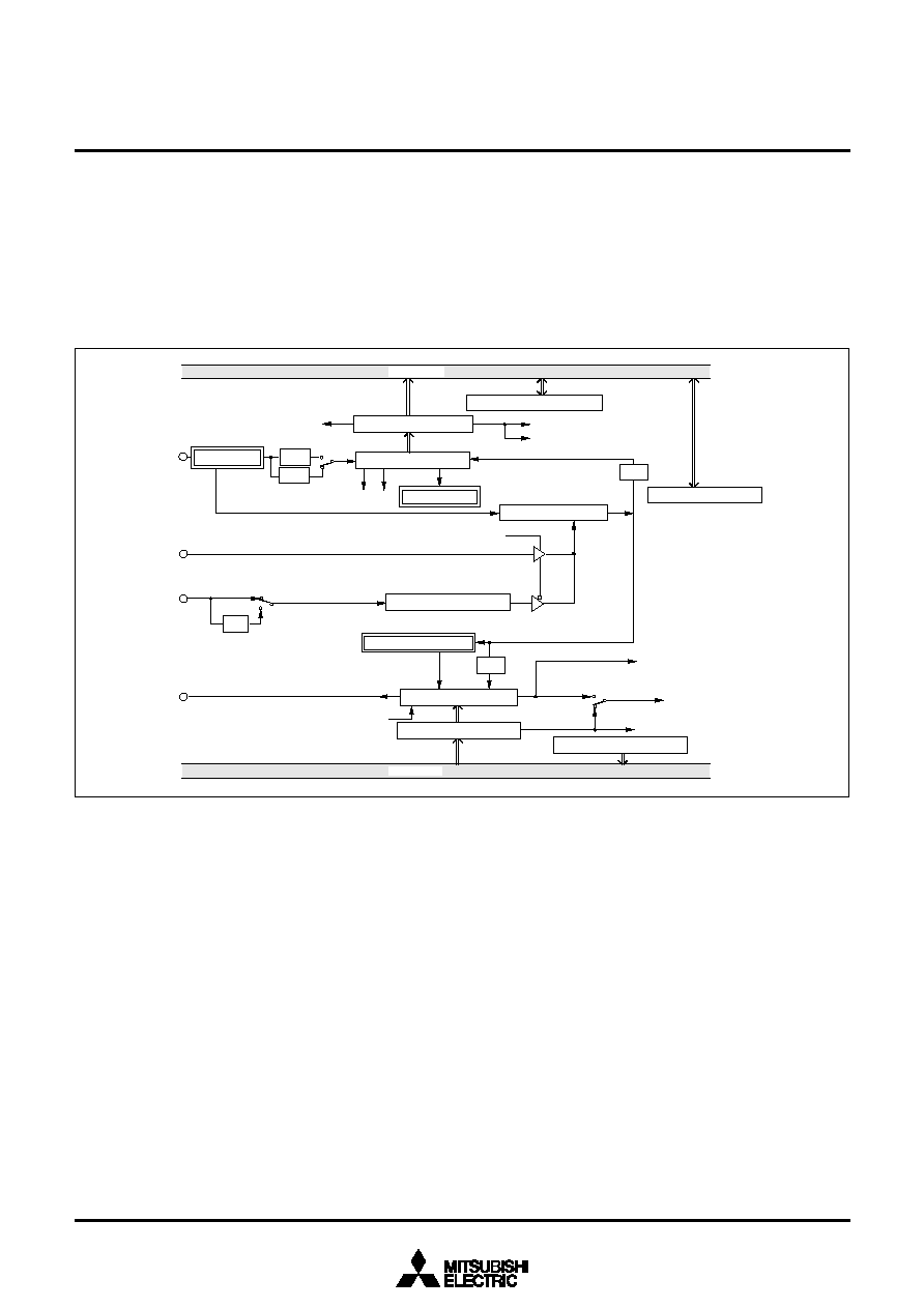
33
SINGLE-CHIP 8-BIT CMOS MICROCOMPUTER
MITSUBISHI MICROCOMPUTERS
(2) Asynchronous Serial I/O (UART) Mode
Clock asynchronous serial I/O mode (UART) can be selected by
clearing the serial I/O1 mode selection bit (b6) of the serial I/O1
control register to "0".
Eight serial data transfer formats can be selected, and the transfer
formats used by a transmitter and receiver must be identical.
The transmit and receive shift registers each have a buffer, but the
two buffers have the same address in memory. Since the shift reg-
ister cannot be written to or read from directly, transmit data is
written to the transmit buffer register, and receive data is read
from the receive buffer register.
The transmit buffer register can also hold the next data to be
transmitted, and the receive buffer register can hold a character
while the next character is being received.
Fig. 28 Block diagram of UART serial I/O1
3850 Group (Spec. H/A)
X
IN
1/4
OE
P
E FE
1
/
1
6
1/16
Data bus
R
e
c
e
i
v
e
b
u
f
f
e
r
r
e
g
i
s
t
e
r
A
d
d
r
e
s
s
0
0
1
8
1
6
R
e
c
e
i
v
e
s
h
i
f
t
r
e
g
i
s
t
e
r
Receive buffer full flag (RBF)
R
e
c
e
i
v
e
i
n
t
e
r
r
u
p
t
r
e
q
u
e
s
t
(
R
I
)
B
a
u
d
r
a
t
e
g
e
n
e
r
a
t
o
r
Frequency division ratio 1/(n+1)
Address 001C
16
ST/SP/PA generator
Transmit buffer register
Data bus
T
r
a
n
s
m
i
t
s
h
i
f
t
r
e
g
i
s
t
e
r
A
d
d
r
e
s
s
0
0
1
8
1
6
Transmit shift completion flag (TSC)
Transmit buffer empty flag (TBE)
Transmit interrupt request (TI)
A
d
d
r
e
s
s
0
0
1
9
1
6
S
T
d
e
t
e
c
t
o
r
SP detector
UART control register
A
d
d
r
e
s
s
0
0
1
B
1
6
C
h
a
r
a
c
t
e
r
l
e
n
g
t
h
s
e
l
e
c
t
i
o
n
b
i
t
A
d
d
r
e
s
s
0
0
1
A
1
6
B
R
G
c
o
u
n
t
s
o
u
r
c
e
s
e
l
e
c
t
i
o
n
b
i
t
Transmit interrupt source selection bit
S
e
r
i
a
l
I
/
O
1
s
y
n
c
h
r
o
n
o
u
s
c
l
o
c
k
s
e
l
e
c
t
i
o
n
b
i
t
Clock control circuit
C
h
a
r
a
c
t
e
r
l
e
n
g
t
h
s
e
l
e
c
t
i
o
n
b
i
t
7
b
i
t
s
8 bits
S
e
r
i
a
l
I
/
O
1
c
o
n
t
r
o
l
r
e
g
i
s
t
e
r
P2
6
/S
CLK
Serial I/O1 status register
P
2
4
/
R
X
D
P
2
5
/
T
X
D
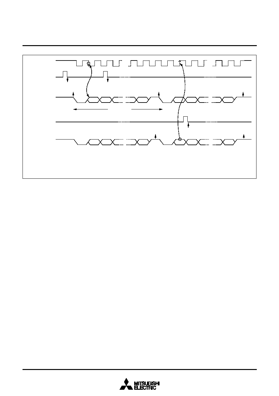
34
SINGLE-CHIP 8-BIT CMOS MICROCOMPUTER
MITSUBISHI MICROCOMPUTERS
Fig. 29 Operation of UART serial I/O1 function
[Transmit Buffer Register/Receive Buffer
Register (TB/RB)] 0018
16
The transmit buffer register and the receive buffer register are lo-
cated at the same address. The transmit buffer is write-only and
the receive buffer is read-only. If a character bit length is 7 bits, the
MSB of data stored in the receive buffer is "0".
[Serial I/O1 Status Register (SIOSTS)] 0019
16
The read-only serial I/O1 status register consists of seven flags
(bits 0 to 6) which indicate the operating status of the serial I/O1
function and various errors.
Three of the flags (bits 4 to 6) are valid only in UART mode.
The receive buffer full flag (bit 1) is cleared to "0" when the receive
buffer register is read.
If there is an error, it is detected at the same time that data is
transferred from the receive shift register to the receive buffer reg-
ister, and the receive buffer full flag is set. A write to the serial I/O1
status register clears all the error flags OE, PE, FE, and SE (bit 3
to bit 6, respectively). Writing "0" to the serial I/O1 enable bit SIOE
(bit 7 of the serial I/O1 control register) also clears all the status
flags, including the error flags.
Bits 0 to 6 of the serial I/O1 status register are initialized to "0" at
reset, but if the transmit enable bit (bit 4) of the serial I/O1 control
register has been set to "1", the transmit shift completion flag (bit
2) and the transmit buffer empty flag (bit 0) become "1".
[Serial I/O1 Control Register (SIOCON)] 001A
16
The serial I/O1 control register consists of eight control bits for the
serial I/O1 function.
[UART Control Register (UARTCON)] 001B
16
The UART control register consists of four control bits (bits 0 to 3)
which are valid when asynchronous serial I/O is selected and set
the data format of an data transfer and one bit (bit 4) which is al-
ways valid and sets the output structure of the P2
5
/T
X
D pin.
[Baud Rate Generator (BRG)] 001C
16
The baud rate generator determines the baud rate for serial trans-
fer.
The baud rate generator divides the frequency of the count source
by 1/(n + 1), where n is the value written to the baud rate genera-
tor.
3850 Group (Spec. H/A)
TSC=0
TBE=1
RBF=0
TBE=0
TBE=0
RBF=1
RBF=1
ST
D
0
D
1
SP
D
0
D
1
ST
SP
TBE=1
TSC=1
ST
D
0
D
1
SP
D
0
D
1
ST
SP
Transmit or receive clock
Transmit buffer write
signal
Generated at 2nd bit in 2-stop-bit mode
1 start bit
7 or 8 data bit
1 or 0 parity bit
1 or 2 stop bit (s)
1: Error flag detection occurs at the same time that the RBF flag becomes "1" (at 1st stop bit, during reception).
2: As the transmit interrupt (TI), when either the TBE or TSC flag becomes "1," can be selected to occur depending on the setting of the transmit
interrupt source selection bit (TIC) of the serial I/O1 control register.
3: The receive interrupt (RI) is set when the RBF flag becomes "1."
4: After data is written to the transmit buffer when TSC=1, 0.5 to 1.5 cycles of the data shift cycle is necessary until changing to TSC=0.
Notes
Serial output T
X
D
Serial input R
X
D
Receive buffer read
signal
35
SINGLE-CHIP 8-BIT CMOS MICROCOMPUTER
MITSUBISHI MICROCOMPUTERS
b
7
T
r
a
n
s
m
i
t
b
u
f
f
e
r
e
m
p
t
y
f
l
a
g
(
T
B
E
)
0
:
B
u
f
f
e
r
f
u
l
l
1
:
B
u
f
f
e
r
e
m
p
t
y
R
e
c
e
i
v
e
b
u
f
f
e
r
f
u
l
l
f
l
a
g
(
R
B
F
)
0
:
B
u
f
f
e
r
e
m
p
t
y
1
:
B
u
f
f
e
r
f
u
l
l
T
r
a
n
s
m
i
t
s
h
i
f
t
c
o
m
p
l
e
t
i
o
n
f
l
a
g
(
T
S
C
)
0
:
T
r
a
n
s
m
i
t
s
h
i
f
t
i
n
p
r
o
g
r
e
s
s
1
:
T
r
a
n
s
m
i
t
s
h
i
f
t
c
o
m
p
l
e
t
e
d
O
v
e
r
r
u
n
e
r
r
o
r
f
l
a
g
(
O
E
)
0
:
N
o
e
r
r
o
r
1
:
O
v
e
r
r
u
n
e
r
r
o
r
P
a
r
i
t
y
e
r
r
o
r
f
l
a
g
(
P
E
)
0
:
N
o
e
r
r
o
r
1
:
P
a
r
i
t
y
e
r
r
o
r
F
r
a
m
i
n
g
e
r
r
o
r
f
l
a
g
(
F
E
)
0
:
N
o
e
r
r
o
r
1
:
F
r
a
m
i
n
g
e
r
r
o
r
S
u
m
m
i
n
g
e
r
r
o
r
f
l
a
g
(
S
E
)
0
:
(
O
E
)
U
(
P
E
)
U
(
F
E
)
=
0
1
:
(
O
E
)
U
(
P
E
)
U
(
F
E
)
=
1
N
o
t
u
s
e
d
(
r
e
t
u
r
n
s
"
1
"
w
h
e
n
r
e
a
d
)
S
e
r
i
a
l
I
/
O
1
s
t
a
t
u
s
r
e
g
i
s
t
e
r
S
e
r
i
a
l
I
/
O
1
c
o
n
t
r
o
l
r
e
g
i
s
t
e
r
b
7
b
0
b
0
B
R
G
c
o
u
n
t
s
o
u
r
c
e
s
e
l
e
c
t
i
o
n
b
i
t
(
C
S
S
)
0
:
f
(
X
I
N
)
1
:
f
(
X
I
N
)
/
4
S
e
r
i
a
l
I
/
O
1
s
y
n
c
h
r
o
n
o
u
s
c
l
o
c
k
s
e
l
e
c
t
i
o
n
b
i
t
(
S
C
S
)
0
:
B
R
G
o
u
t
p
u
t
d
i
v
i
d
e
d
b
y
4
w
h
e
n
c
l
o
c
k
s
y
n
c
h
r
o
n
o
u
s
s
e
r
i
a
l
I
/
O
1
i
s
s
e
l
e
c
t
e
d
,
B
R
G
o
u
t
p
u
t
d
i
v
i
d
e
d
b
y
1
6
w
h
e
n
U
A
R
T
i
s
s
e
l
e
c
t
e
d
.
1
:
E
x
t
e
r
n
a
l
c
l
o
c
k
i
n
p
u
t
w
h
e
n
c
l
o
c
k
s
y
n
c
h
r
o
n
o
u
s
s
e
r
i
a
l
I
/
O
1
i
s
s
e
l
e
c
t
e
d
,
e
x
t
e
r
n
a
l
c
l
o
c
k
i
n
p
u
t
d
i
v
i
d
e
d
b
y
1
6
w
h
e
n
U
A
R
T
i
s
s
e
l
e
c
t
e
d
.
S
R
D
Y
1
o
u
t
p
u
t
e
n
a
b
l
e
b
i
t
(
S
R
D
Y
)
0
:
P
2
7
p
i
n
o
p
e
r
a
t
e
s
a
s
o
r
d
i
n
a
r
y
I
/
O
p
i
n
1
:
P
2
7
p
i
n
o
p
e
r
a
t
e
s
a
s
S
R
D
Y
1
o
u
t
p
u
t
p
i
n
T
r
a
n
s
m
i
t
i
n
t
e
r
r
u
p
t
s
o
u
r
c
e
s
e
l
e
c
t
i
o
n
b
i
t
(
T
I
C
)
0
:
I
n
t
e
r
r
u
p
t
w
h
e
n
t
r
a
n
s
m
i
t
b
u
f
f
e
r
h
a
s
e
m
p
t
i
e
d
1
:
I
n
t
e
r
r
u
p
t
w
h
e
n
t
r
a
n
s
m
i
t
s
h
i
f
t
o
p
e
r
a
t
i
o
n
i
s
c
o
m
p
l
e
t
e
d
T
r
a
n
s
m
i
t
e
n
a
b
l
e
b
i
t
(
T
E
)
0
:
T
r
a
n
s
m
i
t
d
i
s
a
b
l
e
d
1
:
T
r
a
n
s
m
i
t
e
n
a
b
l
e
d
R
e
c
e
i
v
e
e
n
a
b
l
e
b
i
t
(
R
E
)
0
:
R
e
c
e
i
v
e
d
i
s
a
b
l
e
d
1
:
R
e
c
e
i
v
e
e
n
a
b
l
e
d
S
e
r
i
a
l
I
/
O
1
m
o
d
e
s
e
l
e
c
t
i
o
n
b
i
t
(
S
I
O
M
)
0
:
C
l
o
c
k
a
s
y
n
c
h
r
o
n
o
u
s
(
U
A
R
T
)
s
e
r
i
a
l
I
/
O
1
:
C
l
o
c
k
s
y
n
c
h
r
o
n
o
u
s
s
e
r
i
a
l
I
/
O
S
e
r
i
a
l
I
/
O
1
e
n
a
b
l
e
b
i
t
(
S
I
O
E
)
0
:
S
e
r
i
a
l
I
/
O
1
d
i
s
a
b
l
e
d
(
p
i
n
s
P
2
4
t
o
P
2
7
o
p
e
r
a
t
e
a
s
o
r
d
i
n
a
r
y
I
/
O
p
i
n
s
)
1
:
S
e
r
i
a
l
I
/
O
1
e
n
a
b
l
e
d
(
p
i
n
s
P
2
4
t
o
P
2
7
o
p
e
r
a
t
e
a
s
s
e
r
i
a
l
I
/
O
1
p
i
n
s
)
b
7
U
A
R
T
c
o
n
t
r
o
l
r
e
g
i
s
t
e
r
C
h
a
r
a
c
t
e
r
l
e
n
g
t
h
s
e
l
e
c
t
i
o
n
b
i
t
(
C
H
A
S
)
0
:
8
b
i
t
s
1
:
7
b
i
t
s
P
a
r
i
t
y
e
n
a
b
l
e
b
i
t
(
P
A
R
E
)
0
:
P
a
r
i
t
y
c
h
e
c
k
i
n
g
d
i
s
a
b
l
e
d
1
:
P
a
r
i
t
y
c
h
e
c
k
i
n
g
e
n
a
b
l
e
d
P
a
r
i
t
y
s
e
l
e
c
t
i
o
n
b
i
t
(
P
A
R
S
)
0
:
E
v
e
n
p
a
r
i
t
y
1
:
O
d
d
p
a
r
i
t
y
S
t
o
p
b
i
t
l
e
n
g
t
h
s
e
l
e
c
t
i
o
n
b
i
t
(
S
T
P
S
)
0
:
1
s
t
o
p
b
i
t
1
:
2
s
t
o
p
b
i
t
s
P
2
5
/
T
X
D
P
-
c
h
a
n
n
e
l
o
u
t
p
u
t
d
i
s
a
b
l
e
b
i
t
(
P
O
F
F
)
0
:
C
M
O
S
o
u
t
p
u
t
(
i
n
o
u
t
p
u
t
m
o
d
e
)
1
:
N
-
c
h
a
n
n
e
l
o
p
e
n
d
r
a
i
n
o
u
t
p
u
t
(
i
n
o
u
t
p
u
t
m
o
d
e
)
N
o
t
u
s
e
d
(
r
e
t
u
r
n
"
1
"
w
h
e
n
r
e
a
d
)
b
0
(
S
I
O
S
T
S
:
a
d
d
r
e
s
s
0
0
1
9
1
6
)
(
S
I
O
C
O
N
:
a
d
d
r
e
s
s
0
0
1
A
1
6
)
(
U
A
R
T
C
O
N
:
a
d
d
r
e
s
s
0
0
1
B
1
6
)
3850 Group (Spec. H/A)
s
Notes on serial I/O
When setting the transmit enable bit of serial I/O1 to "1", the serial
I/O1 transmit interrupt request bit is automatically set to "1". When
not requiring the interrupt occurrence synchronized with the trans-
mission enalbed, take the following sequence.
Set the serial I/O1 transmit interrupt enable bit to "0" (disabled).
Set the transmit enable bit to "1".
Set the serial I/O1 transmit interrupt request bit to "0" after 1 or
more instructions have been executed.
Set the serial I/O1 transmit interrupt enable bit to "1" (enabled).
Fig. 30 Structure of serial I/O1 control registers

36
SINGLE-CHIP 8-BIT CMOS MICROCOMPUTER
MITSUBISHI MICROCOMPUTERS
q
SERIAL I/O2
The serial I/O2 can be operated only as the clock synchronous type.
As a synchronous clock for serial transfer, either internal clock or
external clock can be selected by the serial I/O2 synchronous clock
selection bit (b6) of serial I/O2 control register 1.
The internal clock incorporates a dedicated divider and permits se-
lecting 6 types of clock by the internal synchronous clock selection
bits (b2, b1, b0) of serial I/O2 control register 1.
Regarding S
OUT2
and S
CLK2
being output pins, either CMOS output
format or N-channel open-drain output format can be selected by the
P0
1
/S
OUT2
, P0
2
/S
CLK2
P-channel output disable bit (b7) of
serial I/O2 control register 1.
When the internal clock has been selected, a transfer starts by a
write signal to the serial I/O2 register (address 0017
16
). After comple-
tion of data transfer, the level of the S
OUT2
pin goes to high imped-
ance automatically but bit 7 of the serial I/O2 control register 2 is not
set to "1" automatically.
When the external clock has been selected, the contents of the serial
I/O2 register is continuously sifted while transfer clocks are input.
Accordingly, control the clock externally. Note that the S
OUT2
pin does
not go to high impedance after completion of data transfer.
To cause the S
OUT2
pin to go to high impedance in the case where
the external clock is selected, set bit 7 of the serial I/O2 control reg-
ister 2 to "1" when S
CLK2
is "H" after completion of data transfer. After
the next data transfer is started (the transfer clock falls), bit 7 of the
serial I/O2 control register 2 is set to "0" and the S
OUT2
pin is put into
the active state.
Regardless of the internal clock to external clock, the interrupt re-
quest bit is set after the number of bits (1 to 8 bits) selected by the
optional transfer bit is transferred. In case of a fractional number of
bits less than 8 bits as the last data, the received data to be stored in
the serial I/O2 register becomes a fractional number of bits close to
MSB if the transfer direction selection bit of serial I/O2 control regis-
ter 1 is LSB first, or a fractional number of bits close to LSB if the
transfer direction selection bit is MSB first. For the remaining bits, the
previously received data is shifted.
At transmit operation using the clock synchronous serial I/O, the S
CMP2
signal can be output by comparing the state of the transmit pin S
OUT2
with the state of the receive pin S
IN2
in synchronization with a rise of
the transfer clock. If the output level of the S
OUT2
pin is equal to the
input level to the S
IN2
pin, "L" is output from the S
CMP2
pin. If not, "H"
is output. At this time, an INT
2
interrupt request can also be gener-
ated. Select a valid edge by bit 2 of the interrupt edge selection reg-
ister (address 003A
16
).
[Serial I/O2 Control Registers 1, 2 (SIO2CON1 /
SIO2CON2)] 0015
16,
0016
16
The serial I/O2 control registers 1 and 2 are containing various se-
lection bits for serial I/O2 control as shown in Figure 31.
Fig. 31 Structure of Serial I/O2 control registers 1, 2
3850 Group (Spec. H/A)
S
e
r
i
a
l
I
/
O
2
c
o
n
t
r
o
l
r
e
g
i
s
t
e
r
1
(
S
I
O
2
C
O
N
1
:
a
d
d
r
e
s
s
0
0
1
5
1
6
)
S
e
r
i
a
l
I
/
O
2
c
o
n
t
r
o
l
r
e
g
i
s
t
e
r
2
(
S
I
O
2
C
O
N
2
:
a
d
d
r
e
s
s
0
0
1
6
1
6
)
b7 b0
O
p
t
i
o
n
a
l
t
r
a
n
s
f
e
r
b
i
t
s
b
2
b
1
b
0
0
0
0
:
1
b
i
t
0
0
1
:
2
b
i
t
0
1
0
:
3
b
i
t
0
1
1
:
4
b
i
t
1
0
0
:
5
b
i
t
1
0
1
:
6
b
i
t
1
1
0
:
7
b
i
t
1
1
1
:
8
b
i
t
N
o
t
u
s
e
d
(
r
e
t
u
r
n
s
"
0
"
w
h
e
n
r
e
a
d
)
S
e
r
i
a
l
I
/
O
2
I
/
O
c
o
m
p
a
r
i
s
o
n
s
i
g
n
a
l
c
o
n
t
r
o
l
b
i
t
0
:
P
4
3
I
/
O
1
:
S
C
M
P
2
o
u
t
p
u
t
S
O
U
T
2
p
i
n
c
o
n
t
r
o
l
b
i
t
(
P
0
1
)
0
:
O
u
t
p
u
t
a
c
t
i
v
e
1
:
O
u
t
p
u
t
h
i
g
h
-
i
m
p
e
d
a
n
c
e
I
n
t
e
r
n
a
l
s
y
n
c
h
r
o
n
o
u
s
c
l
o
c
k
s
e
l
e
c
t
i
o
n
b
i
t
s
b
2
b
1
b
0
0
0
0
:
f
(
X
I
N
)
/
8
(
f
(
X
C
I
N
)
/
8
i
n
l
o
w
-
s
p
e
e
d
m
o
d
e
)
0
0
1
:
f
(
X
I
N
)
/
1
6
(
f
(
X
C
I
N
)
/
1
6
i
n
l
o
w
-
s
p
e
e
d
m
o
d
e
)
0
1
0
:
f
(
X
I
N
)
/
3
2
(
f
(
X
C
I
N
)
/
3
2
i
n
l
o
w
-
s
p
e
e
d
m
o
d
e
)
0
1
1
:
f
(
X
I
N
)
/
6
4
(
f
(
X
C
I
N
)
/
6
4
i
n
l
o
w
-
s
p
e
e
d
m
o
d
e
)
1
1
0
:
f
(
X
I
N
)
/
1
2
8
f
(
X
C
I
N
)
/
1
2
8
i
n
l
o
w
-
s
p
e
e
d
m
o
d
e
)
1
1
1
:
f
(
X
I
N
)
/
2
5
6
(
f
(
X
C
I
N
)
/
2
5
6
i
n
l
o
w
-
s
p
e
e
d
m
o
d
e
)
S
e
r
i
a
l
I
/
O
2
p
o
r
t
s
e
l
e
c
t
i
o
n
b
i
t
0
:
I
/
O
p
o
r
t
1
:
S
O
U
T
2
,
S
C
L
K
2
o
u
t
p
u
t
p
i
n
S
R
D
Y
2
o
u
t
p
u
t
e
n
a
b
l
e
b
i
t
0
:
P
0
3
p
i
n
i
s
n
o
r
m
al
I
/
O
p
i
n
1
:
P
0
3
p
i
n
i
s
S
R
D
Y
2
o
u
t
p
u
t
p
i
n
T
r
a
n
s
f
e
r
d
i
r
e
c
t
i
o
n
s
e
l
e
c
t
i
o
n
b
i
t
0
:
L
S
B
f
i
r
s
t
1
:
M
S
B
f
i
r
s
t
S
e
r
i
a
l
I
/
O
2
s
y
n
c
h
r
o
n
o
u
s
c
l
o
c
k
s
e
l
e
c
t
i
o
n
b
i
t
0
:
E
x
t
e
r
n
a
l
c
l
o
c
k
1
:
I
n
t
e
r
n
a
l
c
l
o
c
k
P
0
1
/
S
O
U
T
2
,
P
0
2
/
S
C
L
K
2
P
-
c
h
a
n
n
e
l
o
u
t
p
u
t
d
i
s
a
b
l
e
b
i
t
0
:
C
M
O
S
o
u
t
p
u
t
(
i
n
o
u
t
p
u
t
m
o
d
e
)
1
:
N
-
c
h
a
n
n
e
l
o
p
e
n
-
d
r
a
i
n
o
u
t
p
u
t
(
i
n
o
u
t
p
u
t
m
o
d
e
)
b
7
b
0
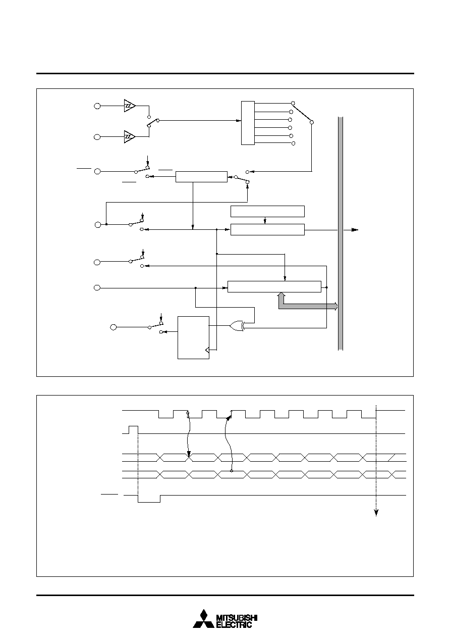
37
SINGLE-CHIP 8-BIT CMOS MICROCOMPUTER
MITSUBISHI MICROCOMPUTERS
3850 Group (Spec. H/A)
Fig. 32 Block diagram of Serial I/O2
Fig. 33 Timing chart of Serial I/O2
X
IN
"1"
"0
"
"0
"
"1"
"0
"
"1
"
S
R
D
Y
2
S
C
L
K
2
"0"
"1
"
1
/
8
1
/
1
6
1
/
3
2
1
/
6
4
1
/
1
2
8
1
/
2
5
6
"1
"
"0"
X
CIN
"1
0
"
"0
0
"
"
0
1
"
Data bus
Serial I/O2
interrupt request
S
e
r
i
a
l
I
/
O
2
p
o
r
t
s
e
l
e
c
t
i
o
n
b
i
t
S
e
r
i
a
l
I
/
O
c
o
u
n
t
e
r
2
(
3
)
S
e
r
i
a
l
I
/
O
2
r
e
g
i
s
t
e
r
(
8
)
S
y
n
c
h
r
o
n
o
u
s
c
i
r
c
u
i
t
S
e
r
i
a
l
I
/
O
2
p
o
r
t
s
e
l
e
c
t
i
o
n
b
i
t
Serial I/O2 synchronous
clock selection bit
S
R
D
Y
2
o
u
t
p
u
t
e
n
a
b
l
e
b
i
t
E
x
t
e
r
n
a
l
c
l
o
c
k
Internal synchronous
clock selection bits
D
i
v
i
d
e
r
Optional transfer bits (3)
P0
2
/S
CLK2
P
0
1
/
S
O
U
T
2
P0
0
/S
IN2
P
0
2
l
a
t
c
h
P
0
1
l
a
t
c
h
P
0
3
l
a
t
c
h
P
0
3
/
S
R
D
Y
2
P4
3
/S
CMP2
/INT
2
Serial I/O2 I/O comparison
signal control bit
P4
3
latch
Q
D
Main clock division ratio
selection bits (Note)
Note: Either high-speed, middle-speed or low-speed mode is selected by bits 6 and 7 of CPU mode register.
D
7
D
0
D
1
D
2
D
3
D
4
D
5
D
6
T
r
a
n
s
f
e
r
c
l
o
c
k
(
N
o
t
e
1
)
S
e
r
i
a
l
I
/
O
2
o
u
t
p
u
t
S
O
U
T
2
S
e
r
i
a
l
I
/
O
2
i
n
p
u
t
S
I
N
2
R
e
c
e
i
v
e
e
n
a
b
l
e
s
i
g
n
a
l
S
R
D
Y
2
W
r
i
t
e
-
i
n
s
i
g
n
a
l
t
o
s
e
r
i
a
l
I
/
O
2
r
e
g
i
s
t
e
r
(
N
o
t
e
2
)
S
e
r
i
a
l
I
/
O
2
i
n
t
e
r
r
u
p
t
r
e
q
u
e
s
t
b
i
t
s
e
t
.
1
:
W
h
e
n
t
h
e
i
n
t
e
r
n
a
l
c
l
o
c
k
i
s
s
e
l
e
c
t
e
d
a
s
a
t
r
a
n
s
f
e
r
c
l
o
c
k
,
t
h
e
f
(
X
I
N
)
c
l
o
c
k
d
i
v
i
s
i
o
n
(
f
(
X
C
I
N
)
i
n
l
o
w
-
s
p
e
e
d
m
o
d
e
)
c
a
n
b
e
s
e
l
e
c
t
e
d
b
y
s
e
t
t
i
n
g
b
i
t
s
0
t
o
2
o
f
s
e
r
i
a
l
I
/
O
2
c
o
n
t
r
o
l
r
e
g
i
s
t
e
r
1
.
2
:
W
h
e
n
t
h
e
i
n
t
e
r
n
a
l
c
l
o
c
k
i
s
s
e
l
e
c
t
e
d
a
s
a
t
r
a
n
s
f
e
r
c
l
o
c
k
,
t
h
e
S
O
U
T
2
p
i
n
h
a
s
h
i
g
h
i
m
p
e
d
a
n
c
e
a
f
t
e
r
t
r
a
n
s
f
e
r
c
o
m
p
l
e
t
i
o
n
.
N
o
t
e
s

38
SINGLE-CHIP 8-BIT CMOS MICROCOMPUTER
MITSUBISHI MICROCOMPUTERS
Fig. 34 S
CMP2
output operation
3850 Group (Spec. H/A)
S
CLK2
S
IN2
S
OUT2
S
CMP2
Judgement of I/O data comparison

39
SINGLE-CHIP 8-BIT CMOS MICROCOMPUTER
MITSUBISHI MICROCOMPUTERS
3850 Group (Spec. H/A)
PULSE WIDTH MODULATION (PWM)
The 3850 group (spec. H/A) has a PWM function with an 8-bit
resolution, based on a signal that is the clock input X
IN
or that
clock input divided by 2.
Data Setting
The PWM output pin also functions as port P4
4
. Set the PWM
period by the PWM prescaler, and set the "H" term of output pulse
by the PWM register.
If the value in the PWM prescaler is n and the value in the PWM
register is m (where n = 0 to 255 and m = 0 to 255) :
PWM period = 255
(n+1) / f(X
IN
)
= 31.875
(n+1)
µ
s
(when f(X
IN
) = 8 MHz,count source selection bit = "0")
Output pulse "H" term = PWM period
m / 255
= 0.125
(n+1)
m
µ
s
(when f(X
IN
) = 8 MHz,count source selection bit = "0")
Fig. 35 Timing of PWM period
Fig. 36 Block diagram of PWM function
PWM Operation
When bit 0 (PWM enable bit) of the PWM control register is set to
"1", operation starts by initializing the PWM output circuit, and
pulses are output starting at an "H".
If the PWM register or PWM prescaler is updated during PWM
output, the pulses will change in the cycle after the one in which
the change was made.
3
1
.
8
7
5
m
(
n
+
1
)
2
5
5
µ
s
T
=
[
3
1
.
8
7
5
(
n
+
1
)
]
µ
s
P
W
M
o
u
t
p
u
t
m
:
C
o
n
t
e
n
t
s
o
f
P
W
M
r
e
g
i
s
t
e
r
n
:
C
o
n
t
e
n
t
s
o
f
P
W
M
p
r
e
s
c
a
l
e
r
T
:
P
W
M
p
e
r
i
o
d
(
w
h
e
n
f
(
X
I
N
)
=
8
M
H
z
,
c
o
u
n
t
s
o
u
r
c
e
s
e
l
e
c
t
i
o
n
b
i
t
=
"
0
"
)
D
a
t
a
b
u
s
Count source
selection bit
"
0
"
"
1
"
PWM
prescaler pre-latch
P
W
M
r
e
g
i
s
t
e
r
p
r
e
-
l
a
t
c
h
PWM
prescaler latch
P
W
M
r
e
g
i
s
t
e
r
l
a
t
c
h
T
r
a
n
s
f
e
r
c
o
n
t
r
o
l
c
i
r
c
u
i
t
P
W
M
r
e
g
i
s
t
e
r
1
/
2
X
IN
P
o
r
t
P
4
4
l
a
t
c
h
P
W
M
e
n
a
b
l
e
b
i
t
P
o
r
t
P
4
4
P
W
M
p
r
e
s
c
a
l
e
r
(X
CIN
at low-speed mode)
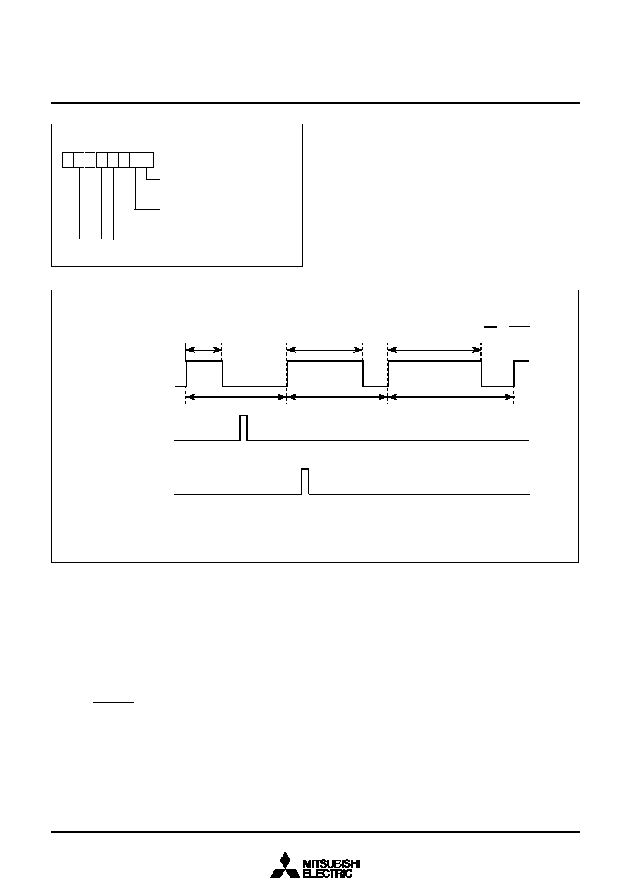
40
SINGLE-CHIP 8-BIT CMOS MICROCOMPUTER
MITSUBISHI MICROCOMPUTERS
Fig. 37 Structure of PWM control register
Fig. 38 PWM output timing when PWM register or PWM prescaler is changed
s
Note
The PWM starts after the PWM function enable bit is set to enable and "L" level is output from the PWM pin.
The length of this "L" level output is as follows:
sec
(Count source selection bit = 0, where n is the value set in the prescaler)
sec
(Count source selection bit = 1, where n is the value set in the prescaler)
n+1
2 ∑ f(X
IN
)
n+1
f(X
IN
)
3850 Group (Spec. H/A)
P
W
M
c
o
n
t
r
o
l
r
e
g
i
s
t
e
r
(
P
W
M
C
O
N
:
a
d
d
r
e
s
s
0
0
1
D
1
6
)
P
W
M
f
u
n
c
t
i
o
n
e
n
a
b
l
e
b
i
t
C
o
u
n
t
s
o
u
r
c
e
s
e
l
e
c
t
i
o
n
b
i
t
N
o
t
u
s
e
d
(
r
e
t
u
r
n
"
0
"
w
h
e
n
r
e
a
d
)
b
7
b
0
0
:
P
W
M
d
i
s
a
b
l
e
d
1
:
P
W
M
e
n
a
b
l
e
d
0
:
f
(
X
I
N
)
(
f
(
X
C
I
N
)
a
t
l
o
w
-
s
p
e
e
d
m
o
d
e
)
1
:
f
(
X
I
N
)
/
2
(
f
(
X
C
I
N
)
/
2
a
t
l
o
w
-
s
p
e
e
d
m
o
d
e
)
A
B
C
B
T
C
T
2
=
P
W
M
o
u
t
p
u
t
P
W
M
r
e
g
i
s
t
e
r
w
r
i
t
e
s
i
g
n
a
l
P
W
M
p
r
e
s
c
a
l
e
r
w
r
i
t
e
s
i
g
n
a
l
(
C
h
a
n
g
e
s
"
H
"
t
e
r
m
f
r
o
m
"
A
"
t
o
"
B
"
.
)
(
C
h
a
n
g
e
s
P
W
M
p
e
r
i
o
d
f
r
o
m
"
T
"
t
o
"
T
2
"
.
)
W
h
e
n
t
h
e
c
o
n
t
e
n
t
s
o
f
t
h
e
P
W
M
r
e
g
i
s
t
e
r
o
r
P
W
M
p
r
e
s
c
a
l
e
r
h
a
v
e
c
h
a
n
g
e
d
,
t
h
e
P
W
M
o
u
t
p
u
t
w
i
l
l
c
h
a
n
g
e
f
r
o
m
t
h
e
n
e
x
t
p
e
r
i
o
d
a
f
t
e
r
t
h
e
c
h
a
n
g
e
.
T
T
T
2

41
SINGLE-CHIP 8-BIT CMOS MICROCOMPUTER
MITSUBISHI MICROCOMPUTERS
3850 Group (Spec. H)
A-D CONVERTER
[A-D Conversion Registers (ADL, ADH)]
0035
16
, 0036
16
The A-D conversion registers are read-only registers that store the
result of an A-D conversion. Do not read these registers during an
A-D conversion.
[A-D Control Register (ADCON)] 0034
16
The AD control register controls the A-D conversion process. Bits
0 to 2 select a specific analog input pin. Bit 4 indicates the
completion of an A-D conversion. The value of this bit remains at
"0" during an A-D conversion and changes to "1" when an A-D
conversion ends. Writing "0" to this bit starts the A-D conversion.
Comparison Voltage Generator
The comparison voltage generator divides the voltage between
AV
SS
and V
REF
into 1024 and outputs the divided voltages.
Channel Selector
The channel selector selects one of ports P3
0
/AN
0
to P3
4
/AN
4
and
inputs the voltage to the comparator.
Comparator and Control Circuit
The comparator and control circuit compare an analog input volt-
age with the comparison voltage, and the result is stored in the
A-D conversion registers. When an A-D conversion is completed,
the control circuit sets the A-D conversion completion bit and the
A-D interrupt request bit to "1".
Note that because the comparator consists of a capacitor cou-
pling, set f(X
IN
) to 500 kHz or more during an A-D conversion.
When the A-D converter is operated at low-speed mode, f(X
IN
)
and f(X
CIN
) do not have the lower limit of frequency, because of
the A-D converter has a built-in self-oscillation circuit.
Fig. 39 Structure of A-D control register (spec. H)
Fig. 40 Structure of A-D conversion registers (spec. H)
Fig. 41 Block diagram of A-D converter (spec. H)
A
-
D
c
o
n
t
r
o
l
r
e
g
i
s
t
e
r
(
A
D
C
O
N
:
a
d
d
r
e
s
s
0
0
3
4
1
6
)
Analog input pin selection bits
0 0 0: P3
0
/AN
0
0 0 1: P3
1
/AN
1
0 1 0: P3
2
/AN
2
0 1 1: P3
3
/AN
3
1 0 0: P3
4
/AN
4
Not used (returns "0" when read)
A-D conversion completion bit
0: Conversion in progress
1: Conversion completed
Not used (returns "0" when read)
b7
b
0
b
2
b
1
b
0
1
0
-
b
i
t
r
e
a
d
i
n
g
(
R
e
a
d
a
d
d
r
e
s
s
0
0
3
6
1
6
b
e
f
o
r
e
0
0
3
5
1
6
)
(
A
d
d
r
e
s
s
0
0
3
6
1
6
)
(
A
d
d
r
e
s
s
0
0
3
5
1
6
)
8
-
b
i
t
r
e
a
d
i
n
g
(
R
e
a
d
o
n
l
y
a
d
d
r
e
s
s
0
0
3
5
1
6
)
(
A
d
d
r
e
s
s
0
0
3
5
1
6
)
b
8
b
7 b
6 b
5 b
4 b
3 b
2 b
1 b
0
b
7
b
0
b
9
b7
b
0
N
o
t
e
:
T
h
e
h
i
g
h
-
o
r
d
e
r
6
b
i
t
s
o
f
a
d
d
r
e
s
s
0
0
3
6
1
6
b
e
c
o
m
e
"
0
"
a
t
r
e
a
d
i
n
g
.
b9 b8 b7 b6 b5 b4 b3 b2
b
7
b0
C
h
a
n
n
e
l
s
e
l
e
c
t
o
r
A-D control circuit
A
-
D
c
o
n
v
e
r
s
i
o
n
l
o
w
-
o
r
d
e
r
r
e
g
i
s
t
e
r
Resistor ladder
V
REF
AV
SS
C
o
m
p
a
r
a
t
o
r
A
-
D
i
n
t
e
r
r
u
p
t
r
e
q
u
e
s
t
b
7
b
0
3
10
P
3
0
/
A
N
0
P
3
1
/
A
N
1
P
3
2
/
A
N
2
P
3
3
/
A
N
3
P
3
4
/
A
N
4
D
a
t
a
b
u
s
A
-
D
c
o
n
t
r
o
l
r
e
g
i
s
t
e
r
A
-
D
c
o
n
v
e
r
s
i
o
n
h
i
g
h
-
o
r
d
e
r
r
e
g
i
s
t
e
r
(
A
d
d
r
e
s
s
0
0
3
4
1
6
)
(Address 0036
16
)
(Address 0035
16
)
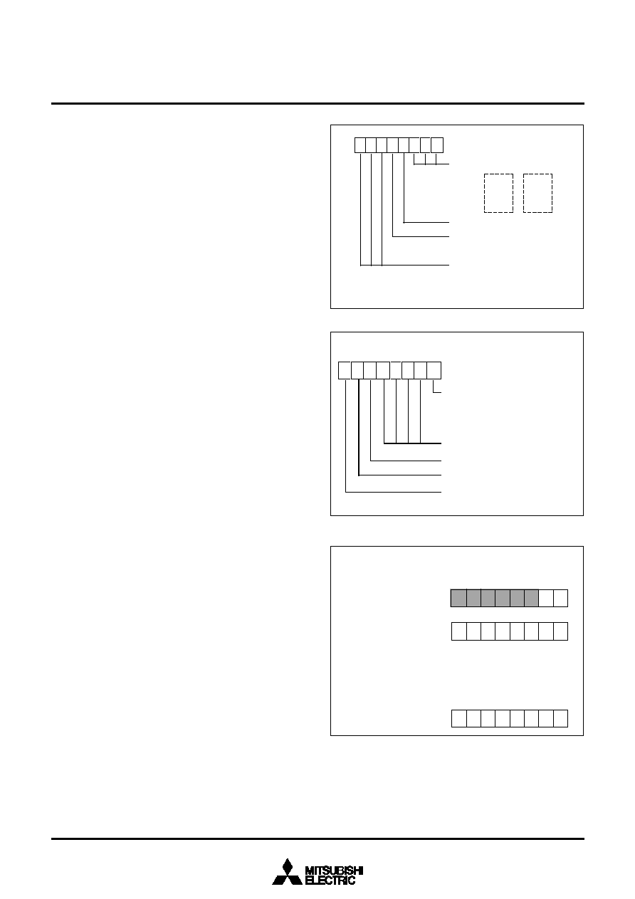
42
SINGLE-CHIP 8-BIT CMOS MICROCOMPUTER
MITSUBISHI MICROCOMPUTERS
A-D CONVERTER
[A-D Conversion Registers (ADL, ADH)]
0035
16
, 0036
16
The A-D conversion registers are read-only registers that store the
result of an A-D conversion. Do not read these registers during an
A-D conversion.
[A-D Control Register (ADCON)] 0034
16
The A-D control register controls the A-D conversion process. Bits
0 to 2 select a specific analog input pin. By setting a value to these
bits, when bit 0 of the A-D input selection register (address
0037
16
) is "0", P3
0
/AN
0
-P3
4
/AN
4
can be selected, and when bit 0
of the A-D input selection register is "1", P0
4
/AN
5
-P0
7
/AN
8
can be
selected.
Bit 4 indicates the completion of an A-D conversion. The value of
this bit remains at "0" during an A-D conversion and changes to "1"
when an A-D conversion ends. Writing "0" to this bit starts the A-D
conversion.
[A-D Input Selection Register (ADSEL)]
0037
16
The analog input port selection switch bit is assigned to bit 0 of the
A-D input selection register. When "0" is set to the analog input
port selection switch bit, P3
0
/AN
0
-P3
4
/AN
4
can be selected by the
analog input pin selection bits (b2, b1, b0) of the A-D control reg-
ister (address 0034
16
). When "1" is set to the analog input port
selection switch bit, P0
4
/AN
5
-P0
7
/AN
8
can be selected by the ana-
log input pin selection bits (b2, b1, b0) of the A-D control register
(address 0034
16
).
Comparison Voltage Generator
The comparison voltage generator divides the voltage between
AV
SS
and V
REF
into 1024 and outputs the divided voltages.
Channel Selector
The channel selector selects one of ports P3
0
/AN
0
to P3
4
/AN
4
,
P0
4
/AN
5
to P0
7
/AN
8
and inputs the voltage to the comparator.
Comparator and Control Circuit
The comparator and control circuit compare an analog input volt-
age with the comparison voltage, and the result is stored in the
A-D conversion registers. When an A-D conversion is completed,
the control circuit sets the A-D conversion completion bit and the
A-D interrupt request bit to "1".
Note that because the comparator consists of a capacitor cou-
pling, set f(X
IN
) to 500 kHz or more during an A-D conversion.
When the A-D converter is operated at low-speed mode, f(X
IN
)
and f(X
CIN
) do not have the lower limit of frequency, because of
the A-D converter has a built-in self-oscillation circuit.
Fig. 42 Structure of A-D control register (spec. A)
Fig. 44 Structure of A-D conversion registers (spec. A)
3850 Group (Spec. A)
Fig. 43 Structure of A-D input selection register (spec. A)
A
-
D
c
o
n
t
r
o
l
r
e
g
i
s
t
e
r
(
A
D
C
O
N
:
a
d
d
r
e
s
s
0
0
3
4
1
6
)
A
n
a
l
o
g
i
n
p
u
t
p
i
n
s
e
l
e
c
t
i
o
n
b
i
t
s
0
0
0
:
P
3
0
/
A
N
0
0
0
1
:
P
3
1
/
A
N
1
0
1
0
:
P
3
2
/
A
N
2
0
1
1
:
P
3
3
/
A
N
3
1
0
0
:
P
3
4
/
A
N
4
N
o
t
u
s
e
d
(
r
e
t
u
r
n
s
"
0
"
w
h
e
n
r
e
a
d
)
A
-
D
c
o
n
v
e
r
s
i
o
n
c
o
m
p
l
e
t
i
o
n
b
i
t
0
:
C
o
n
v
e
r
s
i
o
n
i
n
p
r
o
g
r
e
s
s
1
:
C
o
n
v
e
r
s
i
o
n
c
o
m
p
l
e
t
e
d
N
o
t
u
s
e
d
(
r
e
t
u
r
n
s
"
0
"
w
h
e
n
r
e
a
d
)
b
7
b0
b
2
b
1
b
0
N
o
t
e
1
o
r
o
r
o
r
o
r
P0
4
/AN
5
P0
5
/AN
6
P0
6
/AN
7
P0
7
/AN
8
≠≠≠≠≠≠
N
o
t
e
2
N
o
t
e
s
1
:
T
h
i
s
i
s
s
e
l
e
c
t
e
d
w
h
e
n
b
i
t
0
o
f
t
h
e
A
-
D
i
n
p
u
t
s
e
l
e
c
t
i
o
n
r
e
g
i
s
t
e
r
(
a
d
d
r
e
s
s
0
0
3
7
1
6
)
i
s
"
0
"
.
2
:
T
h
i
s
i
s
s
e
l
e
c
t
e
d
w
h
e
n
b
i
t
0
o
f
t
h
e
A
-
D
i
n
p
u
t
s
e
l
e
c
t
i
o
n
r
e
g
i
s
t
e
r
(
a
d
d
r
e
s
s
0
0
3
7
1
6
)
i
s
"
1
"
.
A-D input selection register
(ADSEL: address 0037
16
)
Analog input port selection switch bit
0: P3
0
/AN
0
toP3
4
/AN
4 is selected as
analog input pin.
1: P0
4
/AN
5
to P0
7
/AN
8 is selected as
analog input pin.
Not used (returns "0" when read)
Fix this bit to "0".
Not used (returns "0" when read)
Fix this bit to "0".
b
7
b
0
1
0
-
b
i
t
r
e
a
d
i
n
g
(
R
e
a
d
a
d
d
r
e
s
s
0
0
3
6
1
6
b
e
f
o
r
e
0
0
3
5
1
6
)
(
A
d
d
r
e
s
s
0
0
3
6
1
6
)
(
A
d
d
r
e
s
s
0
0
3
5
1
6
)
8
-
b
i
t
r
e
a
d
i
n
g
(
R
e
a
d
o
n
l
y
a
d
d
r
e
s
s
0
0
3
5
1
6
)
(
A
d
d
r
e
s
s
0
0
3
5
1
6
)
b
8
b
7 b
6 b
5 b
4 b
3 b
2 b
1 b
0
b
7
b
0
b
9
b
7
b
0
N
o
t
e
:
T
h
e
h
i
g
h
-
o
r
d
e
r
6
b
i
t
s
o
f
a
d
d
r
e
s
s
0
0
3
6
1
6
b
e
c
o
m
e
"
0
"
a
t
r
e
a
d
i
n
g
.
b
9 b
8 b
7 b
6 b
5 b
4 b
3 b
2
b
7
b
0
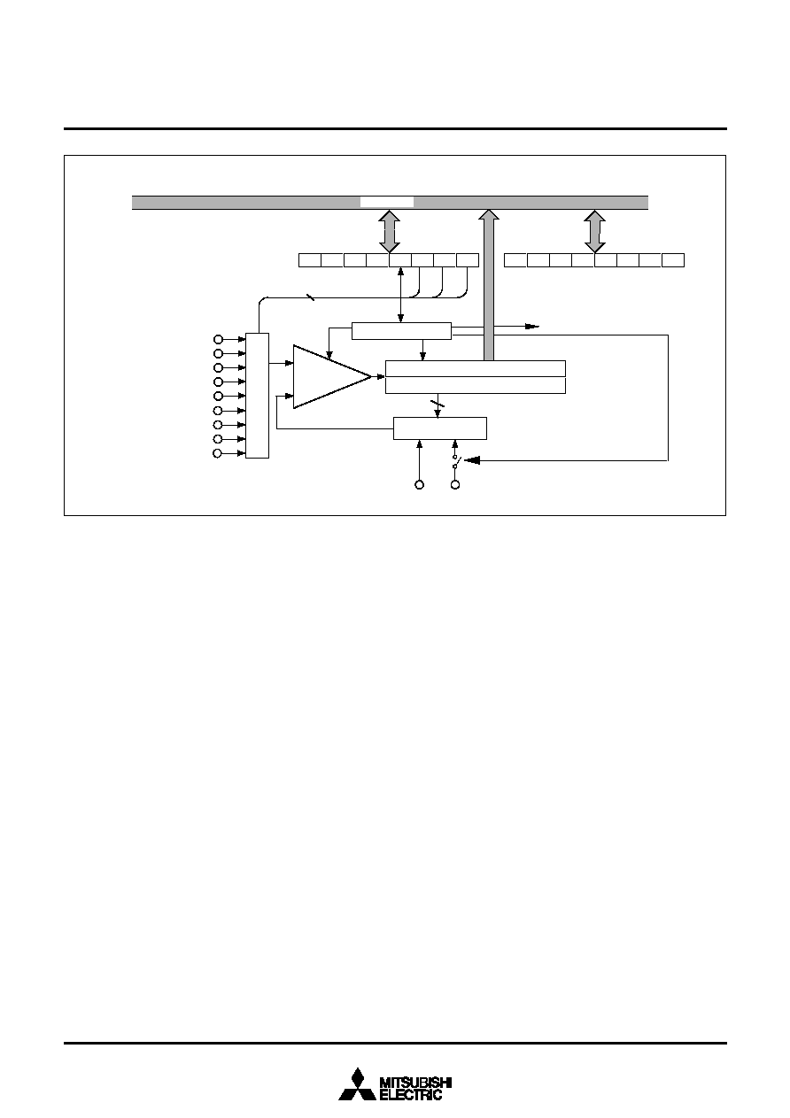
43
SINGLE-CHIP 8-BIT CMOS MICROCOMPUTER
MITSUBISHI MICROCOMPUTERS
Fig. 45 Block diagram of A-D converter (spec. A)
C
h
a
n
n
e
l
s
e
l
e
c
t
o
r
A
-
D
c
o
n
t
r
o
l
c
i
r
c
u
i
t
A
-
D
c
o
n
v
e
r
s
i
o
n
l
o
w
-
o
r
d
e
r
r
e
g
i
s
t
e
r
Resistor ladder
V
REF
AV
SS
C
o
m
p
a
r
a
t
o
r
A
-
D
i
n
t
e
r
r
u
p
t
r
e
q
u
e
s
t
b
7
b0
3
10
P
3
0
/
A
N
0
P
3
1
/
A
N
1
P
3
2
/
A
N
2
P
3
3
/
A
N
3
P
3
4
/
A
N
4
Data bus
A
-
D
c
o
n
t
r
o
l
r
e
g
i
s
t
e
r
A
-
D
c
o
n
v
e
r
s
i
o
n
h
i
g
h
-
o
r
d
e
r
r
e
g
i
s
t
e
r
(
A
d
d
r
e
s
s
0
0
3
4
1
6
)
(
A
d
d
r
e
s
s
0
0
3
6
1
6
)
(
A
d
d
r
e
s
s
0
0
3
5
1
6
)
P0
4
/AN
5
P
0
5
/
A
N
6
P
0
6
/
A
N
7
P
0
7
/
A
N
8
b7
b
0
A-D input selection register
(
A
d
d
r
e
s
s
0
0
3
7
1
6
)
3850 Group (Spec. A)

44
SINGLE-CHIP 8-BIT CMOS MICROCOMPUTER
MITSUBISHI MICROCOMPUTERS
WATCHDOG TIMER
The watchdog timer gives a mean of returning to the reset status
when a program cannot run on a normal loop (for example, be-
cause of a software run-away). The watchdog timer consists of an
8-bit watchdog timer L and an 8-bit watchdog timer H.
Standard Operation of Watchdog Timer
When any data is not written into the watchdog timer control reg-
ister (address 0039
16
) after reset, the watchdog timer is in the
stop state. The watchdog timer starts to count down by writing an
optional value into the watchdog timer control register (address
0039
16
) and an internal reset occurs at an underflow of the watch-
dog timer H.
Accordingly, programming is usually performed so that writing to
the watchdog timer control register (address 0039
16
) may be
started before an underflow. When the watchdog timer control reg-
ister (address 0039
16
) is read, the values of the high-order 6 bits
of the watchdog timer H, STP instruction disable bit, and watch-
dog timer H count source selection bit are read.
q
Initial value of watchdog timer
At reset or writing to the watchdog timer control register (address
0039
16
), each watchdog timer H and L are set to "FF
16
."
Fig. 47 Structure of Watchdog timer control register
q
Watchdog timer H count source selection bit operation
Bit 7 of the watchdog timer control register (address 0039
16
) per-
mits selecting a watchdog timer H count source. When this bit is
set to "0", the count source becomes the underflow signal of
watchdog timer L. The detection time is set to 131.072 ms at f(X
IN
)
= 8 MHz frequency and 32.768 s at f(X
CIN
) = 32 kHz frequency.
When this bit is set to "1", the count source becomes the signal
divided by 16 for f(X
IN
) (or f(X
CIN
)). The detection time in this case
is set to 512
µ
s at f(X
IN
) = 8 MHz frequency and 128 ms at f(X
CIN
)
= 32 kHz frequency. This bit is cleared to "0" after reset.
q
Operation of STP instruction disable bit
Bit 6 of the watchdog timer control register (address 0039
16
) per-
mits disabling the STP instruction when the watchdog timer is in
operation.
When this bit is "0", the STP instruction is enabled.
When this bit is "1", the STP instruction is disabled, once the STP
instruction is executed, an internal reset occurs. When this bit is
set to "1", it cannot be rewritten to "0" by program. This bit is
cleared to "0" after reset.
Fig. 46 Block diagram of Watchdog timer
3850 Group (Spec. H/A)
X
IN
Data bus
X
CIN
"
1
0
"
"
0
0
"
"
0
1
"
Main clock division
ratio selection bits
(Note)
"
0
"
"
1
"
1
/
1
6
Watchdog timer H count
source selection bit
R
e
s
e
t
c
i
r
c
u
i
t
STP instruction disable bit
W
a
t
c
h
d
o
g
t
i
m
e
r
H
(
8
)
"
F
F
1
6
"
i
s
s
e
t
w
h
e
n
w
a
t
c
h
d
o
g
t
i
m
e
r
c
o
n
t
r
o
l
r
e
g
i
s
t
e
r
i
s
w
r
i
t
t
e
n
t
o
.
I
n
t
e
r
n
a
l
r
e
s
e
t
R
E
S
E
T
W
a
t
c
h
d
o
g
t
i
m
e
r
L
(
8
)
N
o
t
e
:
A
n
y
o
n
e
o
f
h
i
g
h
-
s
p
e
e
d
,
m
i
d
d
l
e
-
s
p
e
e
d
o
r
l
o
w
-
s
p
e
e
d
m
o
d
e
i
s
s
e
l
e
c
t
e
d
b
y
b
i
t
s
7
a
n
d
6
o
f
t
h
e
C
P
U
m
o
d
e
r
e
g
i
s
t
e
r
.
STP instruction
"FF
16
" is set when
watchdog timer
control register is
written to.
b
0
STP instruction disable bit
0: STP instruction enabled
1: STP instruction disabled
Watchdog timer H count source selection bit
0: Watchdog timer L underflow
1: f(X
IN
)/16 or f(X
CIN
)/16
W
a
t
c
h
d
o
g
t
i
m
e
r
H
(
f
o
r
r
e
a
d
-
o
u
t
o
f
h
i
g
h
-
o
r
d
e
r
6
b
i
t
)
Watchdog timer control register
(WDTCON : address 0039
16
)
b
7
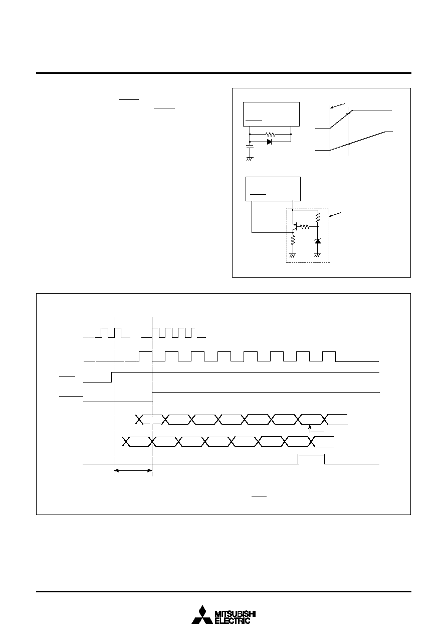
45
SINGLE-CHIP 8-BIT CMOS MICROCOMPUTER
MITSUBISHI MICROCOMPUTERS
3850 Group (Spec. H/A)
RESET CIRCUIT
To reset the microcomputer, RESET pin must be held at an "L"
level for 20 cycles or more of X
IN
. Then the RESET pin is returned
to an "H" level (the power source voltage must be between 2.7 V
and 5.5 V, and the oscillation must be stable), reset is released.
After the reset is completed, the program starts from the address
contained in address FFFD
16
(high-order byte) and address
FFFC
16
(low-order byte). Make sure that the reset input voltage is
less than 0.54 V for V
CC
of 2.7 V.
Fig. 49 Reset sequence
Fig. 48 Reset circuit example
(Note)
0
.
2
V
C
C
0V
0V
P
o
w
e
r
o
n
V
C
C
R
E
S
E
T
V
C
C
R
E
S
E
T
P
o
w
e
r
s
o
u
r
c
e
v
o
l
t
a
g
e
d
e
t
e
c
t
i
o
n
c
i
r
c
u
i
t
P
o
w
e
r
s
o
u
r
c
e
v
o
l
t
a
g
e
R
e
s
e
t
i
n
p
u
t
v
o
l
t
a
g
e
N
o
t
e :
R
e
s
e
t
r
e
l
e
a
s
e
v
o
l
t
a
g
e
;
V
c
c
=
2
.
7
V
R
E
S
E
T
D
a
t
a
A
d
d
r
e
s
s
S
Y
N
C
X
I
N
:
8
t
o
1
3
c
l
o
c
k
c
y
c
l
e
s
X
I
N
?
?
?
?
?
FFFC
F
F
F
D
A
D
H
,
L
?
?
?
?
?
A
D
L
AD
H
1
:
T
h
e
f
r
e
q
u
e
n
c
y
r
e
l
a
t
i
o
n
o
f
f
(
X
I
N
)
a
n
d
f
(
)
i
s
f
(
X
I
N
)
=
2
∑
f
(
)
.
2
:
T
h
e
q
u
e
s
t
i
o
n
m
a
r
k
s
(
?
)
i
n
d
i
c
a
t
e
a
n
u
n
d
e
f
i
n
e
d
s
t
a
t
e
t
h
a
t
d
e
p
e
n
d
s
o
n
t
h
e
p
r
e
v
i
o
u
s
s
t
a
t
e
.
3
:
A
l
l
s
i
g
n
a
l
s
e
x
c
e
p
t
X
I
N
a
n
d
R
E
S
E
T
a
r
e
i
n
t
e
r
n
a
l
s
.
R
e
s
e
t
a
d
d
r
e
s
s
f
r
o
m
t
h
e
v
e
c
t
o
r
t
a
b
l
e
.
N
o
t
e
s
R
E
S
E
T
O
U
T

46
SINGLE-CHIP 8-BIT CMOS MICROCOMPUTER
MITSUBISHI MICROCOMPUTERS
Fig. 50 Internal status at reset (spec. H)
3850 Group (Spec. H)
Note : X : Not fixed
Since the initial values for other than above mentioned registers and
RAM contents are indefinite at reset, they must be set.
(1)
(2)
(3)
(4)
(5)
(6)
(7)
(8)
(9)
(10)
(11)
(12)
(13)
(14)
(15)
(16)
(17)
(18)
(19)
(20)
(21)
(22)
(23)
(24)
(25)
(26)
(27)
(28)
(29)
(30)
(31)
(32)
(33)
Address Register contents
00
16
00
16
00
16
00
16
00
16
00
16
00
16
00
16
00
16
00
16
00
16
00
16
00
16
FF
16
01
16
00
16
00
16
FF
16
FF
16
FF
16
FF
16
00
16
Port P0 (P0)
Port P0 direction register (P0D)
Port P1 (P1)
Port P1 direction register (P1D)
Port P2 (P2)
Port P2 direction register (P2D)
Port P3 (P3)
Port P3 direction register (P3D)
Port P4 (P4)
Port P4 direction register (P4D)
Serial I/O2 control register 1 (SIO2CON1)
Serial I/O2 control register 2 (SIO2CON2)
Serial I/O2 register (SIO2)
Transmit/Receive buffer register (TB/RB)
Serial I/O1 status register (SIOSTS)
Serial I/O1 control register (SIOCON)
UART control register (UARTCON)
Baud rate generator (BRG)
PWM control register (PWMCON)
PWM prescaler (PREPWM)
PWM register (PWM)
Prescaler 12 (PRE12)
Timer 1 (T1)
Timer 2 (T2)
Timer XY mode register (TM)
Prescaler X (PREX)
Timer X (TX)
Prescaler Y (PREY)
Timer Y (TY)
Timer count source selection register (TCSS)
A-D control register (ADCON)
A-D conversion low-order register (ADL)
A-D conversion high-order register (ADH)
0 0 0 0 0 1 1 1
1 0 0 0 0 0 0 0
X X X X X X X X
0000
16
0001
16
0002
16
0003
16
0004
16
0005
16
0006
16
0007
16
0008
16
0009
16
0015
16
0016
16
0017
16
0018
16
0019
16
001A
16
001B
16
001C
16
001D
16
001E
16
001F
16
0020
16
0021
16
0022
16
0023
16
0024
16
0025
16
0026
16
0027
16
0028
16
0034
16
0035
16
0036
16
1 1 1 0 0 0 0 0
X X X X X X X X
X X X X X X X X
X X X X X X X X
X X X X X X X X
0 0 0 1 0 0 0 0
X X X X X X X X
X X
00
16
00
16
00
16
00
16
00
16
00
16
(34)
(35)
(36)
(37)
(38)
(39)
(40)
(41)
(42)
(43)
Register contents
0038
16
0039
16
003A
16
003B
16
003C
16
003D
16
003E
16
003F
16
(PS)
(PC
H
)
(PC
L
)
Address
X X X X X 1 X X
FFFD
16
contents
FFFC
16
contents
0 0 1 1 1 1 1 1
0 1 0 0 1 0 0 0
MISRG
Watchdog timer control register (WDTCON)
Interrupt edge selection register (INTEDGE)
CPU mode register (CPUM)
Interrupt request register 1 (IREQ1)
Interrupt request register 2 (IREQ2)
Interrupt control register 1 (ICON1)
Interrupt control register 2 (ICON2)
Processor status register
Program counter
0 0 0 0 0 0
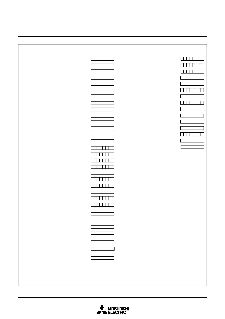
47
SINGLE-CHIP 8-BIT CMOS MICROCOMPUTER
MITSUBISHI MICROCOMPUTERS
Fig. 51 Internal status at reset (spec. A)
3850 Group (Spec. A)
A-D control register (ADCON)
A-D conversion low-order register (ADL)
A-D conversion high-order register (ADH)
A-D input selection register (ADSEL)
MISRG
Watchdog timer control register (WDTCON)
Interrupt edge selection register (INTEDGE)
CPU mode register (CPUM)
Interrupt request register 1 (IREQ1)
Interrupt request register 2 (IREQ2)
Interrupt control register 1 (ICON1)
Interrupt control register 2 (ICON2)
Processor status register
Program counter
Note : X : Not fixed
Since the initial values for other than above mentioned registers and
RAM contents are indefinite at reset, they must be set.
(
1
)
(
2
)
(
3
)
(
4
)
(
5
)
(
6
)
(
7
)
(
8
)
(
9
)
(
1
0
)
(
1
1
)
(
1
2
)
(
1
3
)
(
1
4
)
(
1
5
)
(
1
6
)
(
1
7
)
(
1
8
)
(
1
9
)
(
2
0
)
(
2
1
)
(
2
2
)
(
2
3
)
(
2
4
)
(
2
5
)
(
2
6
)
(
2
7
)
(
2
8
)
(
2
9
)
(
3
0
)
(
3
1
)
(
3
2
)
(
3
3
)
A
d
d
r
e
s
s Register contents
00
16
00
16
00
16
00
16
00
16
00
16
00
16
00
16
00
16
00
16
00
16
00
16
00
16
00
16
00
16
00
16
FF
16
01
16
00
16
00
16
FF
16
FF
16
FF
16
FF
16
00
16
P
o
r
t
P
0
(
P
0
)
P
o
r
t
P
0
d
i
r
e
c
t
i
o
n
r
e
g
i
s
t
e
r
(
P
0
D
)
P
o
r
t
P
1
(
P
1
)
P
o
r
t
P
1
d
i
r
e
c
t
i
o
n
r
e
g
i
s
t
e
r
(
P
1
D
)
P
o
r
t
P
2
(
P
2
)
P
o
r
t
P
2
d
i
r
e
c
t
i
o
n
r
e
g
i
s
t
e
r
(
P
2
D
)
P
o
r
t
P
3
(
P
3
)
P
o
r
t
P
3
d
i
r
e
c
t
i
o
n
r
e
g
i
s
t
e
r
(
P
3
D
)
P
o
r
t
P
4
(
P
4
)
P
o
r
t
P
4
d
i
r
e
c
t
i
o
n
r
e
g
i
s
t
e
r
(
P
4
D
)
P
o
r
t
P
0
,
P
1
,
P
2
p
u
l
l
-
u
p
c
o
n
t
r
o
l
r
e
g
i
s
t
e
r
(
P
U
L
L
0
1
2
)
P
o
r
t
P
3
p
u
l
l
-
u
p
c
o
n
t
r
o
l
r
e
g
i
s
t
e
r
(
P
U
L
L
3
)
P
o
r
t
P
4
p
u
l
l
-
u
p
c
o
n
t
r
o
l
r
e
g
i
s
t
e
r
(
P
U
L
L
4
)
S
e
r
i
a
l
I
/
O
2
c
o
n
t
r
o
l
r
e
g
i
s
t
e
r
1
(
S
I
O
2
C
O
N
1
)
S
e
r
i
a
l
I
/
O
2
c
o
n
t
r
o
l
r
e
g
i
s
t
e
r
2
(
S
I
O
2
C
O
N
2
)
S
e
r
i
a
l
I
/
O
2
r
e
g
i
s
t
e
r
(
S
I
O
2
)
T
r
a
n
s
m
i
t
/
R
e
c
e
i
v
e
b
u
f
f
e
r
r
e
g
i
s
t
e
r
(
T
B
/
R
B
)
S
e
r
i
a
l
I
/
O
1
s
t
a
t
u
s
r
e
g
i
s
t
e
r
(
S
I
O
S
T
S
)
S
e
r
i
a
l
I
/
O
1
c
o
n
t
r
o
l
r
e
g
i
s
t
e
r
(
S
I
O
C
O
N
)
U
A
R
T
c
o
n
t
r
o
l
r
e
g
i
s
t
e
r
(
U
A
R
T
C
O
N
)
B
a
u
d
r
a
t
e
g
e
n
e
r
a
t
o
r
(
B
R
G
)
P
W
M
c
o
n
t
r
o
l
r
e
g
i
s
t
e
r
(
P
W
M
C
O
N
)
P
W
M
p
r
e
s
c
a
l
e
r
(
P
R
E
P
W
M
)
P
W
M
r
e
g
i
s
t
e
r
(
P
W
M
)
P
r
e
s
c
a
l
e
r
1
2
(
P
R
E
1
2
)
T
i
m
e
r
1
(
T
1
)
T
i
m
e
r
2
(
T
2
)
T
i
m
e
r
X
Y
m
o
d
e
r
e
g
i
s
t
e
r
(
T
M
)
P
r
e
s
c
a
l
e
r
X
(
P
R
E
X
)
T
i
m
e
r
X
(
T
X
)
P
r
e
s
c
a
l
e
r
Y
(
P
R
E
Y
)
T
i
m
e
r
Y
(
T
Y
)
T
i
m
e
r
c
o
u
n
t
s
o
u
r
c
e
s
e
l
e
c
t
i
o
n
r
e
g
i
s
t
e
r
(
T
C
S
S
)
0 0 0 0 0 1 1 1
1 0 0 0 0 0 0 0
X X X X X X X X
0
0
0
0
1
6
0
0
0
1
1
6
0
0
0
2
1
6
0
0
0
3
1
6
0
0
0
4
1
6
0
0
0
5
1
6
0
0
0
6
1
6
0
0
0
7
1
6
0
0
0
8
1
6
0
0
0
9
1
6
0
0
1
2
1
6
0
0
1
3
1
6
0
0
1
4
1
6
0
0
1
5
1
6
0
0
1
6
1
6
0
0
1
7
1
6
0
0
1
8
1
6
0
0
1
9
1
6
0
0
1
A
1
6
0
0
1
B
1
6
0
0
1
C
1
6
0
0
1
D
1
6
0
0
1
E
1
6
0
0
1
F
1
6
0
0
2
0
1
6
0
0
2
1
1
6
0
0
2
2
1
6
0
0
2
3
1
6
0
0
2
4
1
6
0
0
2
5
1
6
0
0
2
6
1
6
0
0
2
7
1
6
0
0
2
8
1
6
1 1 1 0 0 0 0 0
X X X X X X X X
X X X X X X X X
X X X X X X X X
X X X X X X X X
0
0
1
6
0
0
1
6
0
0
1
6
0
0
1
6
0
0
1
6
0
0
1
6
0
0
1
6
(34)
(35)
(36)
(37)
(38)
(39)
(40)
(41)
(42)
(43)
(44)
(45)
(46)
(47)
R
e
g
i
s
t
e
r
c
o
n
t
e
n
t
s
0034
16
0035
16
0036
16
0037
16
0038
16
0039
16
003A
16
003B
16
003C
16
003D
16
003E
16
003F
16
(PS)
(PC
H
)
(PC
L
)
Address
X X X X X 1 X X
F
F
F
D
1
6
c
o
n
t
e
n
t
s
F
F
F
C
1
6
c
o
n
t
e
n
t
s
0 0 1 1 1 1 1 1
0 1 0 0 1 0 0 0
0 0 0 1 0 0 0 0
X X X X X X X X
X X
0 0 0 0 0 0

48
SINGLE-CHIP 8-BIT CMOS MICROCOMPUTER
MITSUBISHI MICROCOMPUTERS
CLOCK GENERATING CIRCUIT
The 3850 group (spec. H/A) has two built-in oscillation circuits. An
oscillation circuit can be formed by connecting a resonator be-
tween X
IN
and X
OUT
(X
CIN
and X
COUT
). Use the circuit constants
in accordance with the resonator manufacturer's recommended
values. No external resistor is needed between X
IN
and X
OUT
since a feed-back resistor exists on-chip. However, an external
feed-back resistor is needed between X
CIN
and X
COUT
.
Immediately after power on, only the X
IN
oscillation circuit starts
oscillating, and X
CIN
and X
COUT
pins function as I/O ports.
Frequency Control
(1) Middle-speed mode
The internal clock
is the frequency of X
IN
divided by 8. After re-
set is released, this mode is selected.
(2) High-speed mode
The internal clock
is half the frequency of X
IN
.
(3) Low-speed mode
The internal clock
is half the frequency of X
CIN
.
s
Note
If you switch the mode between middle/high-speed and low-
speed, stabilize both X
IN
and X
CIN
oscillations. The sufficient time
is required for the sub-clock to stabilize, especially immediately af-
ter power on and at returning from the stop mode. When switching
the mode between middle/high-speed and low-speed, set the fre-
quency on condition that f(X
IN
) > 3∑f(X
CIN
).
(4) Low power dissipation mode
The low power consumption operation can be realized by stopping
the main clock X
IN
in low-speed mode. To stop the main clock, set
bit 5 of the CPU mode register to "1." When the main clock X
IN
is
restarted (by setting the main clock stop bit to "0"), set sufficient
time for oscillation to stabilize.
The sub-clock X
CIN
-X
COUT
oscillating circuit can not directly input
clocks that are generated externally. Accordingly, make sure to
cause an external resonator to oscillate.
Oscillation Control
(1) Stop mode
If the STP instruction is executed, the internal clock
stops at an
"H" level, and X
IN
and X
CIN
oscillation stops. When the oscillation
stabilizing time set after STP instruction released bit is "0," the
prescaler 12 is set to "FF
16
" and timer 1 is set to "01
16
." When the
oscillation stabilizing time set after STP instruction released bit is
"1," set the sufficient time for oscillation of used oscillator to stabi-
lize since nothing is set to the prescaler 12 and timer 1.
Either X
IN
or X
CIN
divided by 16 is input to the prescaler 12 as
count source. Oscillator restarts when an external interrupt is re-
ceived, but the internal clock
is not supplied to the CPU (remains
at "H") until timer 1 underflows. The internal clock
is supplied for
the first time, when timer 1 underflows. This ensures time for the
clock oscillation using the ceramic resonators to be stabilized.
When the oscillator is restarted by reset, apply "L" level to the
RESET pin until the oscillation is stable since a wait time will not
be generated.
Fig. 52 Ceramic resonator circuit
Fig. 53 External clock input circuit
(2) Wait mode
If the WIT instruction is executed, the internal clock
stops at an
"H" level, but the oscillator does not stop. The internal clock
re-
starts at reset or when an interrupt is received. Since the oscillator
does not stop, normal operation can be started immediately after
the clock is restarted.
To ensure that the interrupts will be received to release the STP or
WIT state, their interrupt enable bits must be set to "1" before ex-
ecuting of the STP or WIT instruction.
When releasing the STP state, the prescaler 12 and timer 1 will
start counting the clock X
IN
divided by 16. Accordingly, set the
timer 1 interrupt enable bit to "0" before executing the STP instruc-
tion.
s
Note
When using the oscillation stabilizing time set after STP instruction
released bit set to "1", evaluate time to stabilize oscillation of the
used oscillator and set the value to the timer 1 and prescaler 12.
3850 Group (Spec. H/A)
X
C
I
N
X
C
O
U
T
X
I
N
X
O
U
T
C
I
N
C
O
U
T
C
C
I
N
C
C
O
U
T
R
f
R
d
X
C
I
N
X
C
O
U
T
X
I
N
X
O
U
T
C
C
I
N
C
C
O
U
T
R
f
R
d
O
p
e
n
E
x
t
e
r
n
a
l
o
s
c
i
l
l
a
t
i
o
n
c
i
r
c
u
i
t
V
c
c
V
s
s
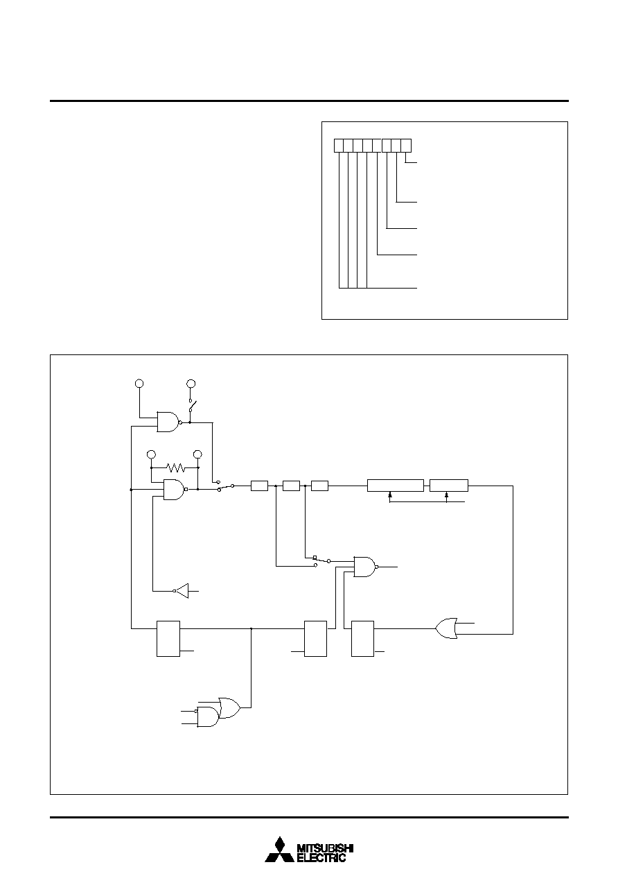
49
SINGLE-CHIP 8-BIT CMOS MICROCOMPUTER
MITSUBISHI MICROCOMPUTERS
Fig. 54 Structure of MISRG
[MISRG (MISRG)] 0038
16
MISRG consists of three control bits (bits 1 to 3) for middle-speed
mode automatic switch and one control bit (bit 0) for oscillation
stabilizing time set after STP instruction released.
By setting the middle-speed mode automatic switch start bit to "1"
while operating in the low-speed mode and setting the middle-
speed mode automatic switch set bit to "1", X
IN
oscillation
automatically starts and the mode is automatically switched to the
middle-speed mode.
Fig. 55 System clock generating circuit block diagram (Single-chip mode)
3850 Group (Spec. H/A)
M
I
S
R
G
(
M
I
S
R
G
:
a
d
d
r
e
s
s
0
0
3
8
1
6
)
O
s
c
i
l
l
a
t
i
o
n
s
t
a
b
i
l
i
z
i
n
g
t
i
m
e
s
e
t
a
f
t
e
r
S
T
P
i
n
s
t
r
u
c
t
i
o
n
r
e
l
e
a
s
e
d
b
i
t
0
:
A
u
t
o
m
a
t
i
c
a
l
l
y
s
e
t
"0
1
1
6
"
t
o
T
i
m
e
r
1
,
"
F
F
1
6
"
t
o
P
r
e
s
c
a
l
e
r
1
2
1
:
A
u
t
o
m
a
t
i
c
a
l
l
y
s
e
t
n
o
t
h
i
n
g
b
7
b
0
N
o
t
e
: W
h
e
n
t
h
e
m
o
d
e
i
s
a
u
t
o
m
a
t
i
c
a
l
l
y
s
w
i
t
c
h
e
d
f
r
o
m
t
h
e
l
o
w
-
s
p
e
e
d
m
o
d
e
t
o
t
h
e
m
i
d
d
l
e
-
s
p
e
e
d
m
o
d
e
,
t
h
e
v
a
l
u
e
o
f
C
P
U
m
o
d
e
r
e
g
i
s
t
e
r
(
a
d
d
r
e
s
s
0
0
3
B
1
6
)
c
h
a
n
g
e
s
.
N
o
t
u
s
e
d
(
r
e
t
u
r
n
"
0
"
w
h
e
n
r
e
a
d
)
M
i
d
d
l
e
-
s
p
e
e
d
m
o
d
e
a
u
t
o
m
a
t
i
c
s
w
i
t
c
h
s
t
a
r
t
b
i
t
(
D
e
p
e
n
d
i
n
g
o
n
p
r
o
g
r
a
m
)
0
:
I
n
v
a
l
i
d
1
:
A
u
t
o
m
a
t
i
c
s
w
i
t
c
h
s
t
a
r
t
M
i
d
d
l
e
-
s
p
e
e
d
m
o
d
e
a
u
t
o
m
a
t
i
c
s
w
i
t
c
h
w
a
i
t
t
i
m
e
s
e
t
b
i
t
0
:
4
.
5
t
o
5
.
5
m
a
c
h
i
n
e
c
y
c
l
e
s
1
:
6
.
5
t
o
7
.
5
m
a
c
h
i
n
e
c
y
c
l
e
s
M
i
d
d
l
e
-
s
p
e
e
d
m
o
d
e
a
u
t
o
m
a
t
i
c
s
w
i
t
c
h
s
e
t
b
i
t
0
:
N
o
t
s
e
t
a
u
t
o
m
a
t
i
c
a
l
l
y
1
:
A
u
t
o
m
a
t
i
c
s
w
i
t
c
h
i
n
g
e
n
a
b
l
e
W
I
T
i
n
s
t
r
u
c
t
i
o
n
STP instruction
T
i
m
i
n
g
(
i
n
t
e
r
n
a
l
c
l
o
c
k
)
S
R
Q
S
T
P
i
n
s
t
r
u
c
t
i
o
n
S
R
Q
M
a
i
n
c
l
o
c
k
s
t
o
p
b
i
t
S
R
Q
1
/
2
1/4
X
IN
X
OUT
X
C
O
U
T
X
C
I
N
I
n
t
e
r
r
u
p
t
r
e
q
u
e
s
t
R
e
s
e
t
I
n
t
e
r
r
u
p
t
d
i
s
a
b
l
e
f
l
a
g
l
1
/
2
P
o
r
t
X
C
s
w
i
t
c
h
b
i
t
"
1
"
"
0
"
Low-speed mode
H
i
g
h
-
s
p
e
e
d
o
r
m
i
d
d
l
e
-
s
p
e
e
d
m
o
d
e
Middle-speed mode
High-speed or
low-speed mode
M
a
i
n
c
l
o
c
k
d
i
v
i
s
i
o
n
r
a
t
i
o
s
e
l
e
c
t
i
o
n
b
i
t
s
(
N
o
t
e
1
)
N
o
t
e
s
1
:
A
n
y
o
n
e
o
f
h
i
g
h
-
s
p
e
e
d
,
m
i
d
d
l
e
-
s
p
e
e
d
o
r
l
o
w
-
s
p
e
e
d
m
o
d
e
i
s
s
e
l
e
c
t
e
d
b
y
b
i
t
s
7
a
n
d
6
o
f
t
h
e
C
P
U
m
o
d
e
r
e
g
i
s
t
e
r
.
W
h
e
n
l
o
w
-
s
p
e
e
d
m
o
d
e
i
s
s
e
l
e
c
t
e
d
,
s
e
t
p
o
r
t
X
c
s
w
i
t
c
h
b
i
t
(
b
4
)
t
o
"
1
"
.
2
:
W
h
e
n
b
i
t
0
o
f
M
I
S
R
G
=
"
0
"
M
a
i
n
c
l
o
c
k
d
i
v
i
s
i
o
n
r
a
t
i
o
s
e
l
e
c
t
i
o
n
b
i
t
s
(
N
o
t
e
1
)
FF
16
01
16
P
r
e
s
c
a
l
e
r
1
2
Timer 1
Reset or
STP instruction
(Note 2)
R
e
s
e
t
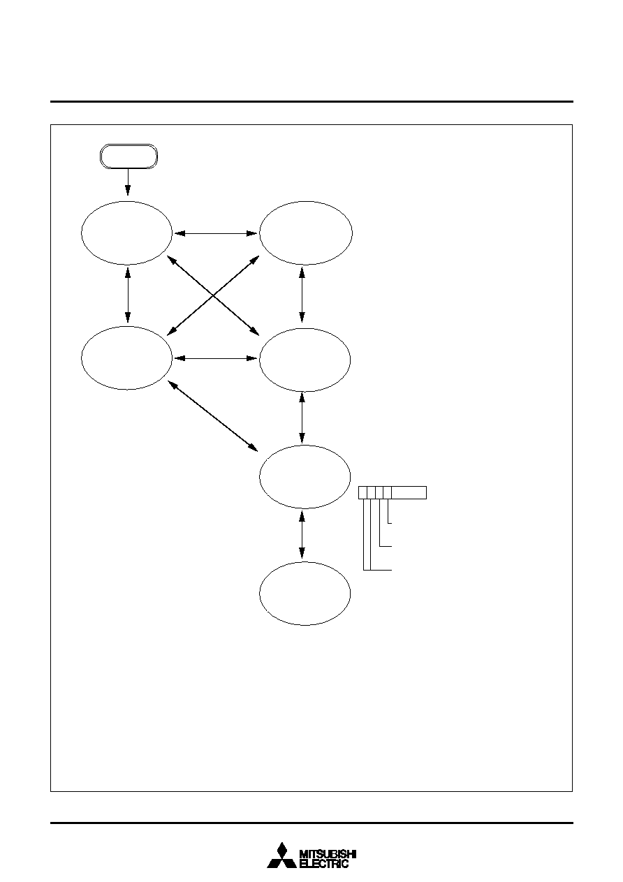
50
SINGLE-CHIP 8-BIT CMOS MICROCOMPUTER
MITSUBISHI MICROCOMPUTERS
Fig. 56 State transitions of system clock
3850 Group (Spec. H/A)
C
M
4
:
P
o
r
t
X
c
s
w
i
t
c
h
b
i
t
0
:
I
/
O
p
o
r
t
f
u
n
c
t
i
o
n
(
s
t
o
p
o
s
c
i
l
l
a
t
i
n
g
)
1
:
X
C
I
N
-
X
C
O
U
T
o
s
c
i
l
l
a
t
i
n
g
f
u
n
c
t
i
o
n
C
M
5
:
M
a
i
n
c
l
o
c
k
(
X
I
N
-
X
O
U
T
)
s
t
o
p
b
i
t
0
:
O
p
e
r
a
t
i
n
g
1
:
S
t
o
p
p
e
d
C
M
7
,
C
M
6
:
M
a
i
n
c
l
o
c
k
d
i
v
i
s
i
o
n
r
a
t
i
o
s
e
l
e
c
t
i
o
n
b
i
t
b
7
b
6
0
0
:
=
f
(
X
I
N
)
/
2
(
H
i
g
h
-
s
p
e
e
d
m
o
d
e
)
0
1
:
=
f
(
X
I
N
)
/
8
(
M
i
d
d
l
e
-
s
p
e
e
d
m
o
d
e
)
1
0
:
=
f
(
X
C
I
N
)
/
2
(
L
o
w
-
s
p
e
e
d
m
o
d
e
)
1
1
:
N
o
t
a
v
a
i
l
a
b
l
e
N
o
t
e
s
R
e
s
e
t
C
M
4
"
1
"
"
0
"
C
M
4
"
0
"
"
1
"
C
M
6
"
1
"
"
0
"
C
M
4
"
1
"
"
0
"
C
M
6
"
1
"
"
0
"
C
M
7
"
1
"
"
0
"
C
M
4
"
1
"
"
0
"
C
M
5
"
1
"
"
0
"
C
M
6
"
1
"
"
0
"
C
M
6
"
1
"
"
0
"
C
P
U
m
o
d
e
r
e
g
i
s
t
e
r
b7
b
4
C
M
7
"
0
"
"
1
"
C
M
6
"
1
"
"
0
"
(
C
P
U
M
:
a
d
d
r
e
s
s
0
0
3
B
1
6
)
C
M
7
=
0
C
M
6
=
1
C
M
5
=
0
(
8
M
H
z
o
s
c
i
l
l
a
t
i
n
g
)
C
M
4
=
0
(
3
2
k
H
z
s
t
o
p
p
e
d
)
M
i
d
d
l
e
-
s
p
e
e
d
m
o
d
e
(
f
(
)
=
1
M
H
z
)
C
M
7
=
0
C
M
6
=
1
C
M
5
=
0
(
8
M
H
z
o
s
c
i
l
l
a
t
i
n
g
)
C
M
4
=
1
(
3
2
k
H
z
o
s
c
i
l
l
a
t
i
n
g
)
M
i
d
d
l
e
-
s
p
e
e
d
m
o
d
e
(
f
(
)
=
1
M
H
z
)
C
M
7
=
0
C
M
6
=
0
C
M
5
=
0
(
8
M
H
z
o
s
c
i
l
l
a
t
i
n
g
)
C
M
4
=
0
(
3
2
k
H
z
s
t
o
p
p
e
d
)
H
i
g
h
-
s
p
e
e
d
m
o
d
e
(
f
(
)
=
4
M
H
z
)
C
M
7
=
1
C
M
6
=
0
C
M
5
=
0
(
8
M
H
z
o
s
c
i
l
l
a
t
i
n
g
)
C
M
4
=
1
(
3
2
k
H
z
o
s
c
i
l
l
a
t
i
n
g
)
Low-speed mode
(f(
)=16 kHz)
CM
7
= 1
CM
6
= 0
CM
5
= 1 (8 MHz stopped)
CM
4
= 1 (32 kHz oscillating)
L
o
w
-
s
p
e
e
d
m
o
d
e
(
f
(
)
=
1
6
k
H
z
)
C
M
7
=
0
C
M
6
=
0
C
M
5
=
0
(
8
M
H
z
o
s
c
i
l
l
a
t
i
n
g
)
C
M
4
=
1
(
3
2
k
H
z
o
s
c
i
l
l
a
t
i
n
g
)
High-speed mode
(f(
) = 4 MHz)
1
:
S
w
i
t
c
h
t
h
e
m
o
d
e
b
y
t
h
e
a
l
l
o
w
s
s
h
o
w
n
b
e
t
w
e
e
n
t
h
e
m
o
d
e
b
l
o
c
k
s
.
(
D
o
n
o
t
s
w
i
t
c
h
b
e
t
w
e
e
n
t
h
e
m
o
d
e
s
d
i
r
e
c
t
l
y
w
i
t
h
o
u
t
a
n
a
l
l
o
w
.
)
2
:
T
h
e
a
l
l
m
o
d
e
s
c
a
n
b
e
s
w
i
t
c
h
e
d
t
o
t
h
e
s
t
o
p
m
o
d
e
o
r
t
h
e
w
a
i
t
m
o
d
e
a
n
d
r
e
t
u
r
n
t
o
t
h
e
s
o
u
r
c
e
m
o
d
e
w
h
e
n
t
h
e
s
t
o
p
m
o
d
e
o
r
t
h
e
w
a
i
t
m
o
d
e
i
s
e
n
d
e
d
.
3
:
T
i
m
e
r
o
p
e
r
a
t
e
s
i
n
t
h
e
w
a
i
t
m
o
d
e
.
4
:
W
h
e
n
b
i
t
0
o
f
M
I
S
R
G
i
s
"
0
"
a
n
d
t
h
e
s
t
o
p
m
o
d
e
i
s
e
n
d
e
d
,
a
d
e
l
a
y
o
f
a
p
p
r
o
x
i
m
a
t
e
l
y
1
m
s
o
c
c
u
r
s
b
y
c
o
n
n
e
c
t
i
n
g
t
i
m
e
r
1
i
n
m
i
d
d
l
e
/
h
i
g
h
-
s
p
e
e
d
m
o
d
e
.
5
:
W
h
e
n
b
i
t
0
o
f
M
I
S
R
G
i
s
"
0
"
a
n
d
t
h
e
s
t
o
p
m
o
d
e
i
s
e
n
d
e
d
,
t
h
e
f
o
l
l
o
w
i
n
g
i
s
p
e
r
f
o
r
m
e
d
.
(
1
)
A
f
t
e
r
t
h
e
c
l
o
c
k
i
s
r
e
s
t
a
r
t
e
d
,
a
d
e
l
a
y
o
f
a
p
p
r
o
x
i
m
a
t
e
l
y
2
5
6
m
s
o
c
c
u
r
s
i
n
l
o
w
-
s
p
e
e
d
m
o
d
e
i
f
T
i
m
e
r
1
2
c
o
u
n
t
s
o
u
r
c
e
s
e
l
e
c
t
i
o
n
b
i
t
i
s
"
0
"
.
(
2
)
A
f
t
e
r
t
h
e
c
l
o
c
k
i
s
r
e
s
t
a
r
t
e
d
,
a
d
e
l
a
y
o
f
a
p
p
r
o
x
i
m
a
t
e
l
y
1
6
m
s
o
c
c
u
r
s
i
n
l
o
w
-
s
p
e
e
d
m
o
d
e
i
f
T
i
m
e
r
1
2
c
o
u
n
t
s
o
u
r
c
e
s
e
l
e
c
t
i
o
n
b
i
t
i
s
"
1
"
.
6
: W
a
i
t
u
n
t
i
l
o
s
c
i
l
l
a
t
i
o
n
s
t
a
b
i
l
i
z
e
s
a
f
t
e
r
o
s
c
i
l
l
a
t
i
n
g
t
h
e
m
a
i
n
c
l
o
c
k
X
I
N
b
e
f
o
r
e
t
h
e
s
w
i
t
c
h
i
n
g
f
r
o
m
t
h
e
l
o
w
-
s
p
e
e
d
m
o
d
e
t
o
m
i
d
d
l
e
/
h
i
g
h
-
s
p
e
e
d
m
o
d
e
.
7
:
T
h
e
e
x
a
m
p
l
e
a
s
s
u
m
e
s
t
h
a
t
8
M
H
z
i
s
b
e
i
n
g
a
p
p
l
i
e
d
t
o
t
h
e
X
I
N
p
i
n
a
n
d
3
2
k
H
z
t
o
t
h
e
X
C
I
N
p
i
n
.
i
n
d
i
c
a
t
e
s
t
h
e
i
n
t
e
r
n
a
l
c
l
o
c
k
.
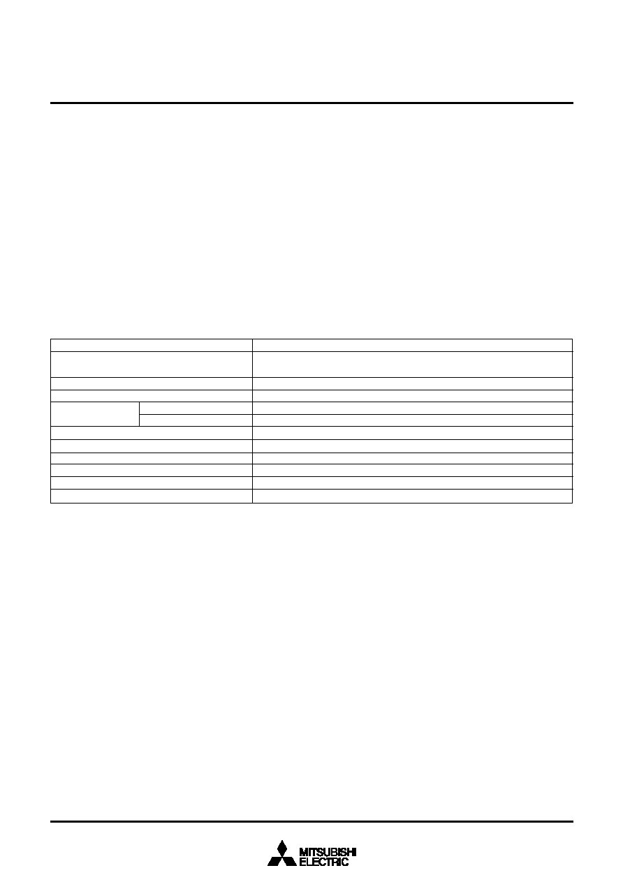
51
3850 Group (Spec. H/A)
SINGLE-CHIP 8-BIT CMOS MICROCOMPUTER
MITSUBISHI MICROCOMPUTERS
Table 11 Summary of M38507F8 (flash memory version)
FLASH MEMORY MODE
The M38507F8 (flash memory version) has an internal new
DINOR (DIvided bit line NOR) flash memory that can be rewritten
with a single power source when V
CC
is 5 V, and 2 power sources
when V
PP
is 5 V and V
CC
is 3.0-5.5 V in the CPU rewrite and stan-
dard serial I/O modes.
For this flash memory, three flash memory modes are available in
which to read, program, and erase: the parallel I/O and standard
serial I/O modes in which the flash memory can be manipulated
using a programmer and the CPU rewrite mode in which the flash
memory can be manipulated by the Central Processing Unit
(CPU).
Summary
Table 11 lists the summary of the M38507F8 (flash memory ver-
sion).
The flash memory of the M38507F8 is divided into User ROM area
and Boot ROM area as shown in Figure 57.
In addition to the ordinary User ROM area to store the MCU op-
eration control program, the flash memory has a Boot ROM area
that is used to store a program to control rewriting in CPU rewrite
and standard serial I/O modes. This Boot ROM area has had a
standard serial I/O mode control program stored in it when
shipped from the factory. However, the user can write a rewrite
control program in this area that suits the user's application sys-
tem. This Boot ROM area can be rewritten in only parallel I/O
mode.
Item
Power source voltage
V
PP
voltage (For Program/Erase)
Flash memory mode
Erase block division
User ROM area
Boot ROM area
Program method
Erase method
Program/Erase control method
Number of commands
Number of program/Erase times
ROM code protection
Specifications
Vcc = 2.7≠ 5.5 V (Note 1)
Vcc = 2.7≠3.6 V (Note 2)
4.5-5.5 V
3 modes (Parallel I/O mode, Standard serial I/O mode, CPU rewrite mode)
1 block (32 Kbytes)
1 block (4 Kbytes) (Note 3)
Byte program
Batch erasing
Program/Erase control by software command
6 commands
100 times
Available in parallel I/O mode and standard serial I/O mode
Notes 1: The power source voltage must be Vcc = 4.5≠5.5 V at program and erase operation.
2: The power source voltage can be Vcc = 3.0≠3.6 V also at program and erase operation.
3: The Boot ROM area has had a standard serial I/O mode control program stored in it when shipped from the factory. This Boot ROM area can be
rewritten in only parallel I/O mode.
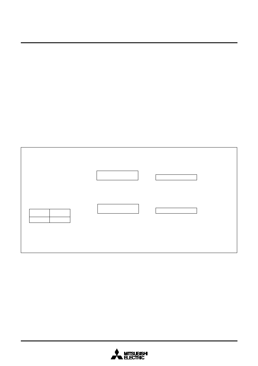
52
3850 Group (Spec. H/A)
SINGLE-CHIP 8-BIT CMOS MICROCOMPUTER
MITSUBISHI MICROCOMPUTERS
Fig. 57 Block diagram of built-in flash memory
(1) CPU Rewrite Mode
In CPU rewrite mode, the internal flash memory can be operated
on (read, program, or erase) under control of the Central Process-
ing Unit (CPU).
In CPU rewrite mode, only the User ROM area shown in Figure 57
can be rewritten; the Boot ROM area cannot be rewritten. Make
sure the program and block erase commands are issued for only
the User ROM area and each block area.
The control program for CPU rewrite mode can be stored in either
User ROM or Boot ROM area. In the CPU rewrite mode, because
the flash memory cannot be read from the CPU, the rewrite con-
trol program must be transferred to internal RAM area to be
executed before it can be executed.
Microcomputer Mode and Boot Mode
The control program for CPU rewrite mode must be written into
the User ROM or Boot ROM area in parallel I/O mode beforehand.
(If the control program is written into the Boot ROM area, the stan-
dard serial I/O mode becomes unusable.)
See Figure 57 for details about the Boot ROM area.
Normal microcomputer mode is entered when the microcomputer
is reset with pulling CNV
SS
pin low. In this case, the CPU starts
operating using the control program in the User ROM area.
When the microcomputer is reset by pulling the P4
1
/INT
0
pin high,
the CNVss pin high, the CPU starts operating using the control
program in the Boot ROM area (program start address is FFFC
16
,
FFFD
16
fixation). This mode is called the "Boot" mode.
Block Address
Block addresses refer to the maximum address of each block.
These addresses are used in the block erase command. In case
of the M38507F8, it has only one block.
8
0
0
0
1
6
Block 1 : 32 kbyte
U
s
e
r
R
O
M
a
r
e
a
4
kb
y
t
e
F
0
0
0
1
6
FFFF
16
FFFF
16
B
o
o
t
R
O
M
a
r
e
a
N
o
t
e
s
1
:
T
h
e
B
o
o
t
R
O
M
a
r
e
a
c
a
n
b
e
r
e
w
r
i
t
t
e
n
i
n
o
n
l
y
p
a
r
a
l
l
e
l
i
n
p
u
t
/
o
u
t
p
u
t
m
o
d
e
.
(
A
c
c
e
s
s
t
o
a
n
y
o
t
h
e
r
a
r
e
a
s
i
s
i
n
h
i
b
i
t
e
d
.
)
2
:
T
o
s
p
e
c
i
f
y
a
b
l
o
c
k
,
u
s
e
t
h
e
m
a
x
i
m
u
m
a
d
d
r
e
s
s
i
n
t
h
e
b
l
o
c
k
.
P
r
o
d
u
c
t
n
a
m
e
F
l
a
s
h
m
e
m
o
r
y
s
t
a
r
t
a
d
d
r
e
s
s
M
3
8
5
0
7
F
8
80
0
0
1
6
P
a
r
a
l
l
e
l
I
/
O
m
o
d
e
8000
16
B
l
o
c
k
1
:
3
2
k
b
y
t
e
F
F
F
F
1
6
C
P
U
r
e
w
r
i
t
e
m
o
d
e
,
s
t
a
n
d
a
r
d
s
e
r
i
a
l
I
/
O
m
o
d
e
U
s
e
r
R
O
M
a
r
e
a
4
kb
y
t
e
F
0
0
0
1
6
F
F
F
F
1
6
B
o
o
t
R
O
M
a
r
e
a
BSEL = 0
BSEL = 1
User area / Boot area selection bit = 0
User area / Boot area selection bit = 1
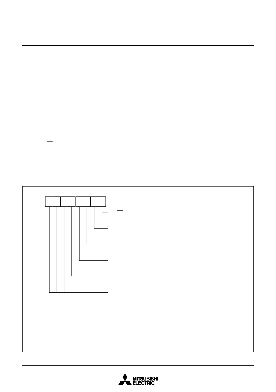
53
3850 Group (Spec. H/A)
SINGLE-CHIP 8-BIT CMOS MICROCOMPUTER
MITSUBISHI MICROCOMPUTERS
Outline Performance (CPU Rewrite Mode)
CPU rewrite mode is usable in the single-chip or Boot mode. The
only User ROM area can be rewritten in CPU rewrite mode.
In CPU rewrite mode, the CPU erases, programs and reads the in-
ternal flash memory by executing software commands. This
rewrite control program must be transferred to the RAM before it
can be executed.
The MCU enters CPU rewrite mode by applying 5 V ± 0.5 V to the
CNV
SS
pin and setting "1" to the CPU Rewrite Mode Select Bit (bit
1 of address 0FFE
16
). Software commands are accepted once the
mode is entered.
Use software commands to control program and erase operations.
Whether a program or erase operation has terminated normally or
in error can be verified by reading the status register.
Figure 58 shows the flash memory control register.
Bit 0 is the RY/BY status flag used exclusively to read the operat-
ing status of the flash memory. During programming and erase
operations, it is "0" (busy). Otherwise, it is "1" (ready).
Bit 1 is the CPU Rewrite Mode Select Bit. When this bit is set to
"1", the MCU enters CPU rewrite mode. Software commands are
accepted once the mode is entered. In CPU rewrite mode, the
CPU becomes unable to access the internal flash memory directly.
Therefore, use the control program in the RAM for write to bit 1. To
set this bit to "1", it is necessary to write "0" and then write "1" in
succession. The bit can be set to "0" by only writing "0".
Bit 2 is the CPU Rewrite Mode Entry Flag. This flag indicates "1" in
CPU rewrite mode, so that reading this flag can check whether
CPU rewrite mode has been entered or not.
Bit 3 is the flash memory reset bit used to reset the control circuit
of internal flash memory. This bit is used when exiting CPU rewrite
mode and when flash memory access has failed. When the CPU
Rewrite Mode Select Bit is "1", setting "1" for this bit resets the
control circuit. To set this bit to "1", it is necessary to write "0" and
then write "1" in succession. To release the reset, it is necessary
to set this bit to "0".
Bit 4 is the User Area/Boot Area Select Bit. When this bit is set to
"1", Boot ROM area is accessed, and CPU rewrite mode in Boot
ROM area is available. In Boot mode, this bit is set to "1" auto-
matically. Reprogramming of this bit must be in the RAM.
Figure 59 shows a flowchart for setting/releasing CPU rewrite
mode.
Fig.58 Structure of flash memory control register
F
l
a
s
h
m
e
m
o
r
y
c
o
n
t
r
o
l
r
e
g
i
s
t
e
r
(
a
d
d
r
e
s
s
0
F
F
E
1
6
)
(
N
o
t
e
1
)
F
M
C
R
RY/BY status flag
0: Busy (being programmed or erased)
1: Ready
CPU rewrite mode select bit (Note 2)
0: Normal mode (Software commands invalid)
1: CPU rewrite mode (Software commands acceptable)
CPU rewrite mode entry flag
0: Normal mode
1: CPU rewrite mode
Flash memory reset bit (Note 3)
0: Normal operation
1: Reset
User ROM area / Boot ROM area select bit
(Note 4)
0: User ROM area accessed
1: Boot ROM area accessed
Reserved bits (Indefinite at read/ "0" at write)
b0
b7
N
o
t
e
s 1:
T
h
e
c
o
n
t
e
n
t
s
o
f
f
l
a
s
h
m
e
m
o
r
y
c
o
n
t
r
o
l
r
e
g
i
s
t
e
r
a
r
e
"
X
X
X
0
0
0
0
1
"
j
u
s
t
a
f
t
e
r
r
e
s
e
t
r
e
l
e
a
s
e
.
I
n
t
h
e
m
a
s
k
R
O
M
v
e
r
s
i
o
n
,
t
h
i
s
a
d
d
r
e
s
s
i
s
r
e
s
e
r
v
e
d
a
r
e
a
.
2:
F
o
r
t
h
i
s
b
i
t
t
o
b
e
s
e
t
t
o
"
1
"
,
t
h
e
u
s
e
r
n
e
e
d
s
t
o
w
r
i
t
e
"
0
"
a
n
d
t
h
e
n
"
1
"
t
o
i
t
i
n
s
u
c
c
e
s
s
i
o
n
.
I
f
i
t
i
s
n
o
t
t
h
i
s
p
r
o
c
e
d
u
r
e
,
t
h
i
s
b
i
t
w
i
l
l
n
o
t
b
e
s
e
t
t
o
"
1
"
.
A
d
d
i
t
i
o
n
a
l
l
y
,
i
t
i
s
r
e
q
u
i
r
e
d
t
o
e
n
s
u
r
e
t
h
a
t
n
o
i
n
t
e
r
r
u
p
t
w
i
l
l
b
e
g
e
n
e
r
a
t
e
d
d
u
r
i
n
g
t
h
a
t
i
n
t
e
r
v
a
l
.
U
s
e
t
h
e
c
o
n
t
r
o
l
p
r
o
g
r
a
m
i
n
t
h
e
a
r
e
a
e
x
c
e
p
t
t
h
e
b
u
i
l
t
-
i
n
f
l
a
s
h
m
e
m
o
r
y
f
o
r
w
r
i
t
e
t
o
t
h
i
s
b
i
t
.
3:
T
h
i
s
b
i
t
i
s
v
a
l
i
d
w
h
e
n
t
h
e
C
P
U
r
e
w
r
i
t
e
m
o
d
e
s
e
l
e
c
t
b
i
t
i
s
"
1
"
.
S
e
t
t
h
i
s
b
i
t
3
t
o
"
0
"
s
u
b
s
e
q
u
e
n
t
l
y
a
f
t
e
r
s
e
t
t
i
n
g
b
i
t
3
t
o
"
1
"
.
4:
U
s
e
t
h
e
c
o
n
t
r
o
l
p
r
o
g
r
a
m
i
n
t
h
e
a
r
e
a
e
x
c
e
p
t
t
h
e
b
u
i
l
t
-
i
n
f
l
a
s
h
m
e
m
o
r
y
f
o
r
w
r
i
t
e
t
o
t
h
i
s
b
i
t
.
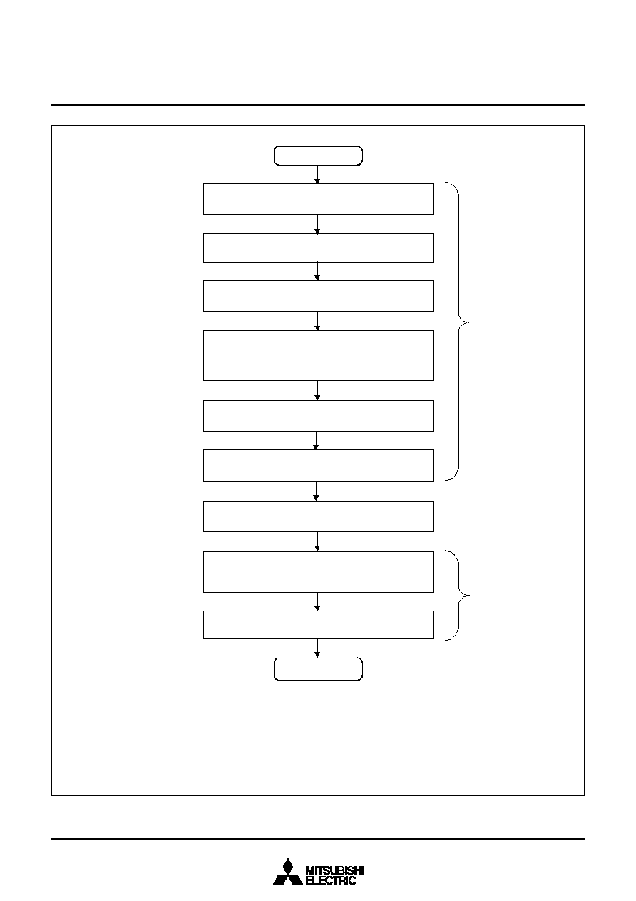
54
3850 Group (Spec. H/A)
SINGLE-CHIP 8-BIT CMOS MICROCOMPUTER
MITSUBISHI MICROCOMPUTERS
Fig. 59 CPU rewrite mode set/release flowchart
End
S
t
a
r
t
E
x
e
c
u
t
e
r
e
a
d
a
r
r
a
y
c
o
m
m
a
n
d
o
r
r
e
s
e
t
f
l
a
s
h
m
e
m
o
r
y
b
y
s
e
t
t
i
n
g
f
l
a
s
h
m
e
m
o
r
y
r
e
s
e
t
b
i
t
(
b
y
w
r
i
t
i
n
g
"
1
"
a
n
d
t
h
e
n
"
0
"
i
n
s
u
c
c
e
s
s
i
o
n
)
(Note 3)
S
i
n
g
l
e
-
c
h
i
p
m
o
d
e
o
r
B
o
o
t
m
o
d
e
(
N
o
t
e
1
)
Set CPU mode register (Note 2)
Using software command execute erase,
program, or other operation
J
u
m
p
t
o
c
o
n
t
r
o
l
p
r
o
g
r
a
m
t
r
a
n
s
f
e
r
r
e
d
i
n
R
A
M
(
S
u
b
s
e
q
u
e
n
t
o
p
e
r
a
t
i
o
n
s
a
r
e
e
x
e
c
u
t
e
d
b
y
c
o
n
t
r
o
l
p
r
o
g
r
a
m
i
n
t
h
i
s
R
A
M
)
T
r
a
n
s
f
e
r
C
P
U
r
e
w
r
i
t
e
m
o
d
e
c
o
n
t
r
o
l
p
r
o
g
r
a
m
t
o
R
A
M
N
o
t
e
s 1:
W
h
e
n
s
t
a
r
t
i
n
g
t
h
e
M
C
U
i
n
t
h
e
s
i
n
g
l
e
-
c
h
i
p
m
o
d
e
,
s
u
p
p
l
y
4
.
5
V
t
o
5
.
2
5
V
t
o
t
h
e
C
N
V
s
s
p
i
n
u
n
t
i
l
c
h
e
c
k
i
n
g
t
h
e
C
P
U
r
e
w
r
i
t
e
m
o
d
e
e
n
t
r
y
f
l
a
g
.
2:
S
e
t
b
i
t
s
6
,
7
(
m
a
i
n
c
l
o
c
k
d
i
v
i
s
i
o
n
r
a
t
i
o
s
e
l
e
c
t
i
o
n
b
i
t
s
)
a
t
C
P
U
m
o
d
e
r
e
g
i
s
t
e
r
(
0
0
3
B
1
6
)
.
3:
B
e
f
o
r
e
e
x
i
t
i
n
g
t
h
e
C
P
U
r
e
w
r
i
t
e
m
o
d
e
a
f
t
e
r
c
o
m
p
l
e
t
i
n
g
e
r
a
s
e
o
r
p
r
o
g
r
a
m
o
p
e
r
a
t
i
o
n
,
a
l
w
a
y
s
b
e
s
u
r
e
t
o
e
x
e
c
u
t
e
t
h
e
r
e
a
d
a
r
r
a
y
c
o
m
m
a
n
d
o
r
r
e
s
e
t
t
h
e
f
l
a
s
h
m
e
m
o
r
y
.
W
r
i
t
e
"
0
"
t
o
C
P
U
r
e
w
r
i
t
e
m
o
d
e
s
e
l
e
c
t
b
i
t
S
e
t
C
P
U
r
e
w
r
i
t
e
m
o
d
e
s
e
l
e
c
t
b
i
t
t
o
"
1
"
(
b
y
w
r
i
t
i
n
g
"
0
"
a
n
d
t
h
e
n
"
1
"
i
n
s
u
c
c
e
s
s
i
o
n
)
C
h
e
c
k
C
P
U
r
e
w
r
i
t
e
m
o
d
e
e
n
t
r
y
f
l
a
g
S
e
t
t
i
n
g
R
e
l
e
a
s
e
d

55
3850 Group (Spec. H/A)
SINGLE-CHIP 8-BIT CMOS MICROCOMPUTER
MITSUBISHI MICROCOMPUTERS
Precautions on CPU Rewrite Mode
Described below are the precautions to be observed when rewriting
the flash memory in CPU rewrite mode.
(1) Operation speed
During CPU rewrite mode, set the internal clock frequency 6.25
MHz or less using the main clock division ratio selection bits (bit
6, 7 at 003B
16
).
(2) Instructions inhibited against use
The instructions which refer to the internal data of the flash
memory cannot be used during CPU rewrite mode .
(3) Interrupts inhibited against use
The interrupts cannot be used during CPU rewrite mode be-
cause they refer to the internal data of the flash memory.
(4) Watchdog timer
In case of the watchdog timer has been running already, the in-
ternal reset generated by watchdog timer underflow does not
happen, because of watchdog timer is always clearing during
program or erase operation.
(5) Reset
Reset is always valid. In case of CNV
SS
= H when reset is re-
leased, boot mode is active. So the program starts from the ad-
dress contained in address FFFC
16
and FFFD
16
in boot ROM
area.
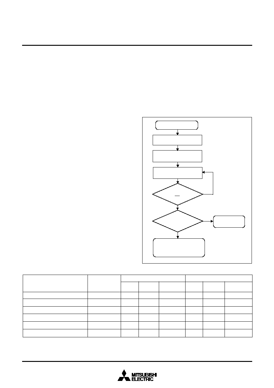
56
3850 Group (Spec. H/A)
SINGLE-CHIP 8-BIT CMOS MICROCOMPUTER
MITSUBISHI MICROCOMPUTERS
Software Commands (CPU Rewrite Mode)
Table 12 lists the software commands.
After setting the CPU Rewrite Mode Select Bit of the flash memory
control register to "1", execute a software command to specify an
erase or program operation.
Each software command is explained below.
q
Read Array Command (FF
16
)
The read array mode is entered by writing the command code
"FF
16
" in the first bus cycle. When an address to be read is input in
one of the bus cycles that follow, the contents of the specified ad-
dress are read out at the data bus (D
0
to D
7
).
The read array mode is retained intact until another command is
written.
q
Read Status Register Command (70
16
)
The read status register mode is entered by writing the command
code "70
16
" in the first bus cycle. The contents of the status regis-
ter are read out at the data bus (D
0
to D
7
) by a read in the second
bus cycle.
The status register is explained in the next section.
q
Clear Status Register Command (50
16
)
This command is used to clear the bits SR1, SR4, and SR5 of the
status register after they have been set. These bits indicate that
operation has ended in an error. To use this command, write the
command code "50
16
" in the first bus cycle.
q
Program Command (40
16
)
Program operation starts when the command code "40
16
" is writ-
ten in the first bus cycle. Then, if the address and data to program
are written in the 2nd bus cycle, program operation (data program-
ming and verification) will start.
Whether the write operation is completed can be confirmed by
_____
reading the status register or the RY/BY Status Flag of the flash
memory control register. When the program starts, the read status
Table 12 List of software commands (CPU rewrite mode)
register mode is entered automatically and the contents of the sta-
tus register is read at the data bus (D
0
to D
7
). The status register
bit 7 (SR7) is set to "0" at the same time the write operation starts
and is returned to "1" upon completion of the write operation. In
this case, the read status register mode remains active until the
next command is written.
____
The RY/BY Status Flag is "0" (busy) during write operation and "1"
(ready) when the write operation is completed as is the status reg-
ister bit 7.
At program end, program results can be checked by reading bit 4
(SR4) of the status register.
Fig. 60 Program flowchart
S
t
a
r
t
Write 40
16
S
t
a
t
u
s
r
e
g
i
s
t
e
r
r
e
a
d
Program completed
(Read array command
"FF
16
" write)
NO
Y
E
S
W
r
i
t
e
a
d
d
r
e
s
s
W
r
i
t
e
d
a
t
a
S
R
4
=
0
?
P
r
o
g
r
a
m
e
r
r
o
r
NO
Y
E
S
S
R
7
=
1
?
o
r
R
Y
/
B
Y
=
1
?
Write
Command
P
r
o
g
r
a
m
C
l
e
a
r
s
t
a
t
u
s
r
e
g
i
s
t
e
r
R
e
a
d
a
r
r
a
y
R
e
a
d
s
t
a
t
u
s
r
e
g
i
s
t
e
r
X
X
First bus cycle
S
e
c
o
n
d
b
u
s
c
y
c
l
e
F
F
1
6
7
0
1
6
5
0
1
6
4
0
1
6
W
r
i
t
e
W
r
i
t
e
W
r
i
t
e
W
r
i
t
e
X
S
R
D
R
e
a
d
W
r
i
t
e
E
r
a
s
e
a
l
l
b
l
o
c
k
s
2
0
1
6
W
r
i
t
e
X
2
0
1
6
W
r
i
t
e
(Note 2)
W
A
(Note 3)
W
D
(
N
o
t
e
3
)
B
l
o
c
k
e
r
a
s
e
2
0
1
6
W
r
i
t
e
D
0
1
6
W
r
i
t
e
B
A
(Note 4)
Mode
Address
Mode
A
d
d
r
e
s
s
Data
(D
0
to D
7
)
(
D
0
t
o
D
7
)
(Note 1)
Notes 1: X denotes a given address in the User ROM area .
2: SRD = Status Register Data
3: WA = Write Address, WD = Write Data
4: BA = Block Address to be erased (Input the maximum address of each block.)
C
y
c
l
e
n
u
m
b
e
r
1
2
1
2
2
2
X
X
X
X
D
a
t
a
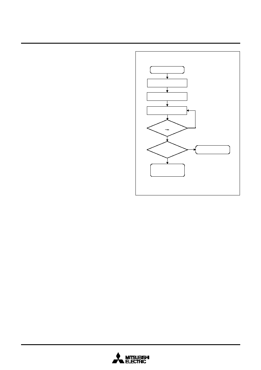
57
3850 Group (Spec. H/A)
SINGLE-CHIP 8-BIT CMOS MICROCOMPUTER
MITSUBISHI MICROCOMPUTERS
q
Erase All Blocks Command (20
16
/20
16
)
By writing the command code "20
16
" in the first bus cycle and the
confirmation command code "20
16
" in the second bus cycle that
follows, the operation of erase all blocks (erase and erase verify)
starts.
Whether the erase all blocks command is terminated can be con-
____
firmed by reading the status register or the RY/BY Status Flag of
flash memory control register. When the erase all blocks operation
starts, the read status register mode is entered automatically and
the contents of the status register can be read out at the data bus
(D
0
to D
7
). The status register bit 7 (SR7) is set to "0" at the same
time the erase operation starts and is returned to "1" upon comple-
tion of the erase operation. In this case, the read status register
mode remains active until another command is written.
____
The RY/BY Status Flag is "0" during erase operation and "1" when
the erase operation is completed as is the status register bit 7
(SR7).
After the erase all blocks end, erase results can be checked by
reading bit 5 (SRS) of the status register. For details, refer to the
section where the status register is detailed.
q
Block Erase Command (20
16
/D0
16
)
By writing the command code "20
16
" in the first bus cycle and the
confirmation command code "D0
16
" and the blobk address in the
second bus cycle that follows, the block erase (erase and erase
verify) operation starts for the block address of the flash memory
to be specified.
Whether the block erase operation is completed can be confirmed
____
by reading the status register or the RY/BY Status Flag of flash
memory control register. At the same time the block erase opera-
tion starts, the read status register mode is automatically entered,
so that the contents of the status register can be read out. The
status register bit 7 (SR7) is set to "0" at the same time the block
erase operation starts and is returned to "1" upon completion of
the block erase operation. In this case, the read status register
mode remains active until the read array command (FF
16
) is writ-
ten.
____
The RY/BY Status Flag is "0" during block erase operation and "1"
when the block erase operation is completed as is the status reg-
ister bit 7.
After the block erase ends, erase results can be checked by read-
ing bit 5 (SRS) of the status register. For details, refer to the
section where the status register is detailed.
Fig. 61 Erase flowchart
W
r
i
t
e
2
0
1
6
20
16
/D0
16
Block address
Erase completed
(Read comand "FF
16
"
write)
N
O
Y
E
S
S
t
a
r
t
Write
S
R
5
=
0
?
E
r
a
s
e
e
r
r
o
r
YES
N
O
2
0
1
6
:
E
r
a
s
e
a
l
l
b
l
o
c
k
s
c
o
m
m
a
n
d
D
0
1
6
:
B
l
o
c
k
e
r
a
s
e
c
o
m
m
a
n
d
SR7 = 1 ?
or
RY/BY = 1 ?
S
t
a
t
u
s
r
e
g
i
s
t
e
r
r
e
a
d
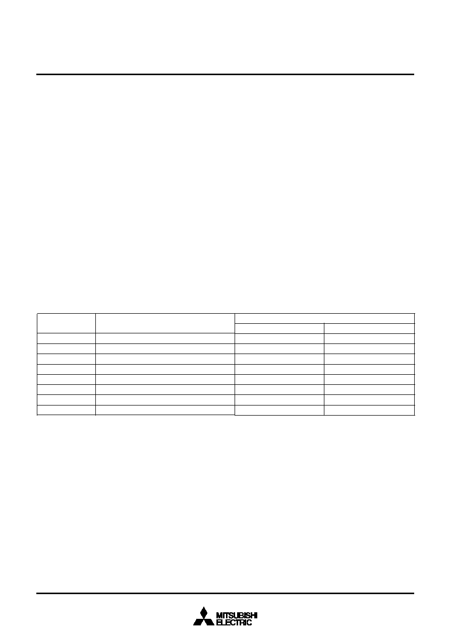
58
3850 Group (Spec. H/A)
SINGLE-CHIP 8-BIT CMOS MICROCOMPUTER
MITSUBISHI MICROCOMPUTERS
Symbol
Table 13 Definition of each bit in status register (SRD)
Status Register (SRD)
The status register shows the operating status of the flash
memory and whether erase operations and programs ended suc-
cessfully or in error. It can be read in the following ways:
(1) By reading an arbitrary address from the User ROM area after
writing the read status register command (70
16
)
(2) By reading an arbitrary address from the User ROM area in the
period from when the program starts or erase operation starts
to when the read array command (FF
16
) is input.
Also, the status register can be cleared by writing the clear status
register command (50
16
).
After reset, the status register is set to "80
16
".
Table 13 shows the status register. Each bit in this register is ex-
plained below.
∑Sequencer status (SR7)
The sequencer status indicates the operating status of the flash
memory. This bit is set to "0" (busy) during write or erase operation
and is set to "1" when these operations ends.
After power-on, the sequencer status is set to "1" (ready).
∑Erase status (SR5)
The erase status indicates the operating status of erase operation.
If an erase error occurs, it is set to "1". When the erase status is
cleared, it is set to "0".
∑Program status (SR4)
The program status indicates the operating status of write opera-
tion. When a write error occurs, it is set to "1".
The program status is set to "0" when it is cleared.
If "1" is written for any of the SR5 and SR4 bits, the program,
erase all blocks, and block erase commands are not accepted.
Before executing these commands, execute the clear status regis-
ter command (50
16
) and clear the status register.
Also, if any commands are not correct, both SR5 and SR4 are set
to "1".
SR7 (bit7)
SR6 (bit6)
SR5 (bit5)
SR4 (bit4)
SR3 (bit3)
SR2 (bit2)
SR1 (bit1)
SR0 (bit0)
Definition
"1" "0"
Status name
Sequencer status
Reserved
Erase status
Program status
Reserved
Reserved
Reserved
Reserved
Ready
-
Terminated in error
Terminated in error
-
-
-
-
Busy
-
Terminated normally
Terminated normally
-
-
-
-

59
3850 Group (Spec. H/A)
SINGLE-CHIP 8-BIT CMOS MICROCOMPUTER
MITSUBISHI MICROCOMPUTERS
Full Status Check
By performing full status check, it is possible to know the execu-
tion results of erase and program operations. Figure 62 shows a
Fig. 62 Full status check flowchart and remedial procedure for errors
full status check flowchart and the action to be taken when each
error occurs.
Read status register
SR4 = 1 and
SR5 = 1 ?
N
O
YES
S
R
5
=
0
?
Y
E
S
Er
a
s
e
e
r
r
o
r
N
O
S
R
4
=
0
?
Y
E
S
N
O
Command
sequence error
Program error
E
n
d
(
e
r
a
s
e
,
p
r
o
g
r
a
m
)
E
x
e
c
u
t
e
t
h
e
c
l
e
a
r
s
t
a
t
u
s
r
e
g
i
s
t
e
r
c
o
m
m
a
n
d
(
5
0
1
6
)
t
o
c
l
e
a
r
t
h
e
s
t
a
t
u
s
r
e
g
i
s
t
e
r
.
T
r
y
p
e
r
f
o
r
m
i
n
g
t
h
e
o
p
e
r
a
t
i
o
n
o
n
e
m
o
r
e
t
i
m
e
a
f
t
e
r
c
o
n
f
i
r
m
i
n
g
t
h
a
t
t
h
e
c
o
m
m
a
n
d
i
s
e
n
t
e
r
e
d
c
o
r
r
e
c
t
l
y
.
S
h
o
u
l
d
a
n
e
r
a
s
e
e
r
r
o
r
o
c
c
u
r
,
t
h
e
b
l
o
c
k
i
n
e
r
r
o
r
c
a
n
n
o
t
b
e
u
s
e
d
.
N
o
t
e:
W
h
e
n
o
n
e
o
f
S
R
5
a
n
d
S
R
4
i
s
s
e
t
t
o
"
1
"
,
n
o
n
e
o
f
t
h
e
r
e
a
d
a
r
r
a
y
,
t
h
e
p
r
o
g
r
a
m
,
e
r
a
s
e
a
l
l
b
l
o
c
k
s
,
a
n
d
b
l
o
c
k
e
r
a
s
e
c
o
m
m
a
n
d
s
i
s
a
c
c
e
p
t
e
d
.
E
x
e
c
u
t
e
t
h
e
c
l
e
a
r
s
t
a
t
u
s
r
e
g
i
s
t
e
r
c
o
m
m
a
n
d
(
5
0
1
6
)
b
e
f
o
r
e
e
x
e
c
u
t
i
n
g
t
h
e
s
e
c
o
m
m
a
n
d
s
.
S
h
o
u
l
d
a
p
r
o
g
r
a
m
e
r
r
o
r
o
c
c
u
r
,
t
h
e
b
l
o
c
k
i
n
e
r
r
o
r
c
a
n
n
o
t
b
e
u
s
e
d
.

60
3850 Group (Spec. H/A)
SINGLE-CHIP 8-BIT CMOS MICROCOMPUTER
MITSUBISHI MICROCOMPUTERS
Functions To Inhibit Rewriting Flash Memory
Version
To prevent the contents of internal flash memory from being read
out or rewritten easily, this MCU incorporates a ROM code protect
function for use in parallel I/O mode and an ID code check func-
tion for use in standard serial I/O mode.
q
ROM Code Protect Function (in Parallel I/O Mode)
The ROM code protect function is the function to inhibit reading
out or modifying the contents of internal flash memory by using
the ROM code protect control (address FFDB
16
) in parallel I/O
mode. Figure 63 shows the ROM code protect control (address
FFDB
16
). (This address exists in the User ROM area.)
If one or both of the pair of ROM Code Protect Bits is set to "0",
the ROM code protect is turned on, so that the contents of internal
flash memory are protected against readout and modification. The
ROM code protect is implemented in two levels. If level 2 is se-
lected, the flash memory is protected even against readout by a
shipment inspection LSI tester, etc. When an attempt is made to
select both level 1 and level 2, level 2 is selected by default.
If both of the two ROM Code Protect Reset Bits are set to "00", the
ROM code protect is turned off, so that the contents of internal
flash memory can be read out or modified. Once the ROM code
protect is turned on, the contents of the ROM Code Protect Reset
Bits cannot be modified in parallel I/O mode. Use the serial I/O or
CPU rewrite mode to rewrite the contents of the ROM Code Pro-
tect Reset Bits.
Fig. 63 Structure of ROM code protect control
R
O
M
c
o
d
e
p
r
o
t
e
c
t
c
o
n
t
r
o
l
r
e
g
i
s
t
e
r
(
a
d
d
r
e
s
s
F
F
D
B
1
6
)
(N
o
t
e
1)
R
O
M
C
P
Reserved bits ("1" at read/write)
ROM code protect level 2 set bits (ROMCP2) (Notes 2, 3)
b3b2
0 0: Protect enabled
0 1: Protect enabled
1 0: Protect enabled
1 1: Protect disabled
ROM code protect reset bits
(Note 4)
b5b4
0 0: Protect removed
0 1: Protect set bits effective
1 0: Protect set bits effective
1 1: Protect set bits effective
ROM code protect level 1 set bits (ROMCP1) (Note 2)
b7b6
0 0: Protect enabled
0 1: Protect enabled
1 0: Protect enabled
1 1: Protect disabled
b
0
b
7
Notes 1: This area is on the ROM in the mask ROM version.
2: When ROM code protect is turned on, the internal flash memory is protected
against readout or modification in parallel I/O mode.
3: When ROM code protect level 2 is turned on, ROM code readout by a shipment
inspection LSI tester, etc. also is inhibited.
4: The ROM code protect reset bits can be used to turn off ROM code protect level 1
and ROM code protect level 2. However, since these bits cannot be modified in
parallel I/O mode, they need to be rewritten in standard serial I/O mode or CPU
rewrite mode.
1
1
61
3850 Group (Spec. H/A)
SINGLE-CHIP 8-BIT CMOS MICROCOMPUTER
MITSUBISHI MICROCOMPUTERS
ID Code Check Function (in Standard serial
I/O mode)
Use this function in standard serial I/O mode. When the contents
of the flash memory are not blank, the ID code sent from the pro-
grammer is compared with the ID code written in the flash memory
to see if they match. If the ID codes do not match, the commands
sent from the programmer are not accepted. The ID code consists
of 8-bit data, and its areas are FFD4
16
to FFDA
16
. Write a pro-
gram which has had the ID code preset at these addresses to the
flash memory.
Fig. 64 ID code store addresses
ROM code protect control
ID7
ID6
I
D
5
I
D
4
ID3
ID2
I
D
1
FFDB
16
FFDA
16
FFD9
16
F
F
D
8
1
6
F
F
D
7
1
6
F
F
D
6
1
6
F
F
D
5
1
6
F
F
D
4
1
6
A
d
d
r
e
s
s
I
n
t
e
r
r
u
p
t
v
e
c
t
o
r
a
r
e
a

62
3850 Group (Spec. H/A)
SINGLE-CHIP 8-BIT CMOS MICROCOMPUTER
MITSUBISHI MICROCOMPUTERS
(2) Parallel I/O Mode
Parallel I/O mode is the mode which parallel output and input soft-
ware command, address, and data required for the operations
(read, program, erase, etc.) to a built-in flash memory. Use the ex-
clusive external equipment flash programmer which supports the
3850 Group (flash memory version). Refer to each programmer
maker's handling manual for the details of the usage.
User ROM and Boot ROM Areas
In parallel I/O mode, the user ROM and boot ROM areas shown in
Figure 57 can be rewritten. Both areas of flash memory can be oper-
ated on in the same way.
Program and block erase operations can be performed in the user ROM
area. The user ROM area and its block is shown in Figure 57.
The boot ROM area is 4 Kbytes in size. It is located at addresses
F000
16
through FFFF
16
. Make sure program and block erase opera-
tions are always performed within this address range. (Access to any
location outside this address range is prohibited.)
In the Boot ROM area, an erase block operation is applied to only
one 4 Kbyte block. The boot ROM area has had a standard serial I/O
mode control program stored in it when shipped from the Mitsubishi
factory. Therefore, using the device in standard serial I/O mode, you
do not need to write to the boot ROM area.

63
3850 Group (Spec. H/A)
SINGLE-CHIP 8-BIT CMOS MICROCOMPUTER
MITSUBISHI MICROCOMPUTERS
(3) Standard serial I/O Mode
The standard serial I/O mode inputs and outputs the software
commands, addresses and data needed to operate (read, pro-
gram, erase, etc.) the internal flash memory. This I/O is clock
synchronized serial. This mode requires the exclusive external
equipment (serial programmer).
The standard serial I/O mode is different from the parallel I/O
mode in that the CPU controls flash memory rewrite (uses the
CPU rewrite mode), rewrite data input and so forth. The standard
serial I/O mode is started by connecting "H" to the P2
6
(S
CLK
) pin
and "H" to the P4
1
(INT
0
) pin and "H" to the CNV
SS
pin (apply 4.5
V to 5.5 V to Vpp from an external source), and releasing the re-
set operation. (In the ordinary microcomputer mode, set CNVss
pin to "L" level.)
This control program is written in the Boot ROM area when the
product is shipped from Mitsubishi. Accordingly, make note of the
fact that the standard serial I/O mode cannot be used if the Boot
ROM area is rewritten in parallel I/O mode. Figure 65 shows the
pin connection for the standard serial I/O mode.
In standard serial I/O mode, serial data I/O uses the four serial I/O
pins S
CLK1
, RxD, TxD and S
RDY1
(BUSY). The S
CLK1
pin is the
transfer clock input pin through which an external transfer clock is
input. The TxD pin is for CMOS output. The S
RDY1
(BUSY) pin
outputs "L" level when ready for reception and "H" level when re-
ception starts.
Serial data I/O is transferred serially in 8-bit units.
In standard serial I/O mode, only the User ROM area shown in
Figure 44 can be rewritten. The Boot ROM area cannot.
In standard serial I/O mode, a 7-byte ID code is used. When there
is data in the flash memory, commands sent from the peripheral
unit (programmer) are not accepted unless the ID code matches.
Outline Performance (Standard Serial I/O
Mode)
In standard serial I/O mode, software commands, addresses and
data are input and output between the MCU and peripheral units
(serial programmer, etc.) using 4-wire clock-synchronized serial
I/O (serial I/O1).
In reception, software commands, addresses and program data
are synchronized with the rise of the transfer clock that is input to
the S
CLK
pin, and are then input to the MCU via the RxD pin. In
transmission, the read data and status are synchronized with the
fall of the transfer clock, and output from the TxD pin.
The TxD pin is for CMOS output. Transfer is in 8-bit units with LSB
first.
When busy, such as during transmission, reception, erasing or
program execution, the S
RDY1
(BUSY) pin is "H" level. Accord-
ingly, always start the next transfer after the S
RDY1
(BUSY) pin is
"L" level.
Also, data and status registers in a memory can be read after in-
putting software commands. Status, such as the operating state of
the flash memory or whether a program or erase operation ended
successfully or not, can be checked by reading the status register.
Here following explains software commands, status registers, etc.
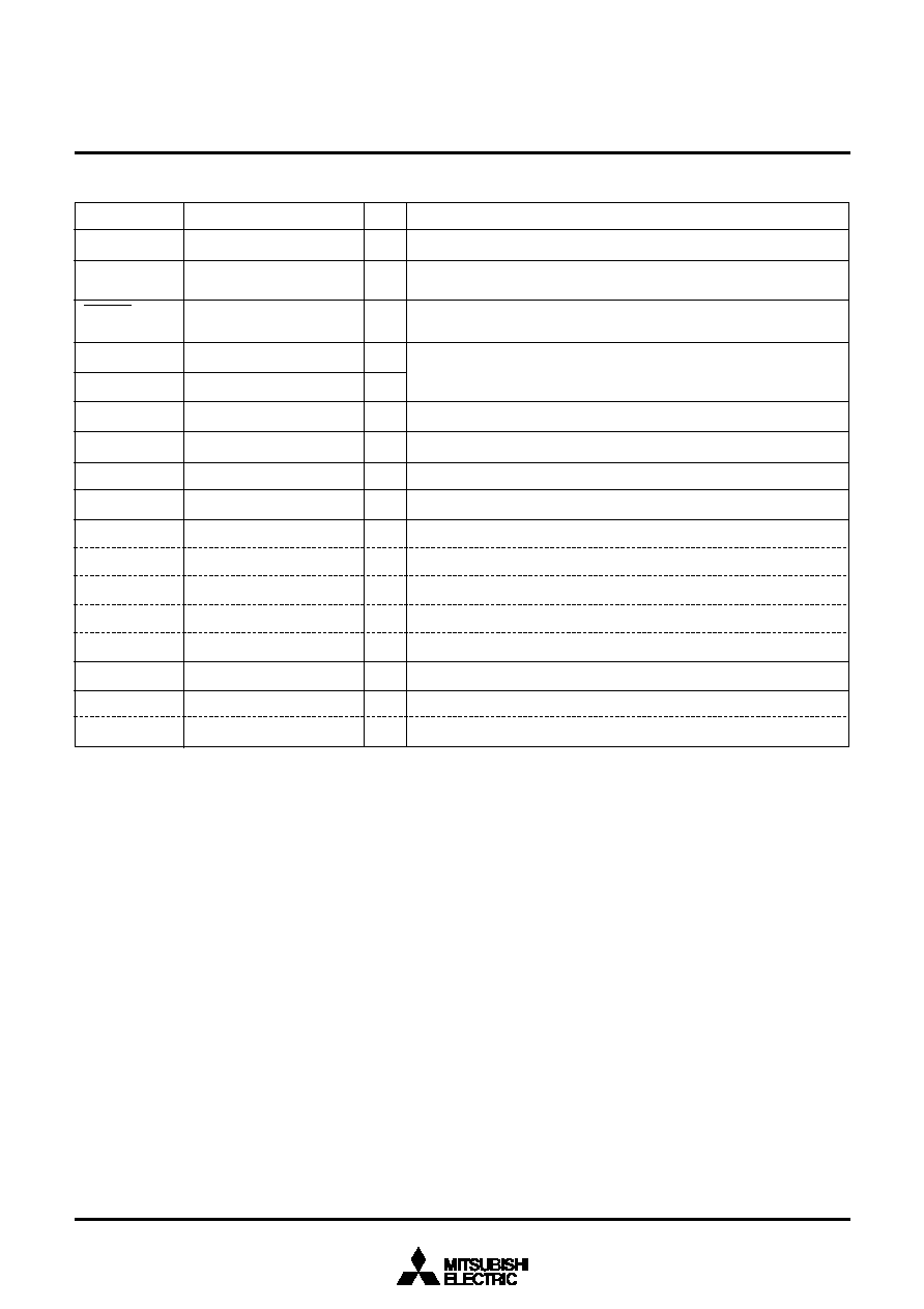
64
3850 Group (Spec. H/A)
SINGLE-CHIP 8-BIT CMOS MICROCOMPUTER
MITSUBISHI MICROCOMPUTERS
Table 14 Description of pin function (Standard Serial I/O Mode)
Pin
D
e
s
c
r
i
p
t
i
o
n
V
C
C
,
V
S
S
Apply program/erase protection voltage to Vcc pin and 0 V to Vss pin.
C
N
V
S
S
Connect to V
CC
when V
CC
= 4.5 V to 5.5 V.
Connect to Vpp (=4.5 V to 5.5 V) when V
CC
= 2.7 V to 4.5 V.
RESET
Reset input pin. While reset is "L" level, a 20 cycle or longer clock
must be input to X
IN
pin.
X
I
N
Connect a ceramic resonator or crystal oscillator between X
IN
and
X
OUT
pins. To input an externally generated clock, input it to X
IN
pin
and open X
OUT
pin.
X
O
U
T
N
a
m
e
P
o
w
e
r
i
n
p
u
t
C
N
V
S
S
R
e
s
e
t
i
n
p
u
t
C
l
o
c
k
i
n
p
u
t
C
l
o
c
k
o
u
t
p
u
t
I/O
I
I
I
O
A
V
S
S
V
R
E
F
C
o
n
n
e
c
t
A
V
S
S
t
o
V
S
S
.
E
n
t
e
r
t
h
e
r
e
f
e
r
e
n
c
e
v
o
l
t
a
g
e
f
o
r
A
D
f
r
o
m
t
h
i
s
p
i
n
.
P0
0
to P0
7
Input "H" or "L" level signal or open.
P1
0
to P1
7
Input "H" or "L" level signal or open.
P
2
0
t
o
P
2
3
I
n
p
u
t
"
H
"
o
r
"
L
"
l
e
v
e
l
s
i
g
n
a
l
o
r
o
p
e
n
.
A
n
a
l
o
g
p
o
w
e
r
s
u
p
p
l
y
i
n
p
u
t
R
e
f
e
r
e
n
c
e
v
o
l
t
a
g
e
i
n
p
u
t
Input port P0
Input port P1
I
n
p
u
t
p
o
r
t
P
2
I
I
I
I
P
4
1
I
n
p
u
t
"
H
"
l
e
v
e
l
s
i
g
n
a
l
,
w
h
e
n
r
e
s
e
t
i
s
r
e
l
e
a
s
e
d
.
P
4
0
,
P
4
2
t
o
P
4
4
I
n
p
u
t
"
H
"
o
r
"
L
"
l
e
v
e
l
s
i
g
n
a
l
o
r
o
p
e
n
.
P
2
4
S
e
r
i
a
l
d
a
t
a
i
n
p
u
t
p
i
n
P2
5
P
2
6
S
e
r
i
a
l
c
l
o
c
k
i
n
p
u
t
p
i
n
P2
7
BUSY signal output pin
I
n
p
u
t
p
o
r
t
P
4
I
n
p
u
t
p
o
r
t
P
4
R
x
D
i
n
p
u
t
TxD output
S
C
L
K
i
n
p
u
t
BUSY output
I
I
O
I
O
Serial data output pin
I
P3
0
to P3
4
Input "H" or "L" level signal or open.
Input port P3
I
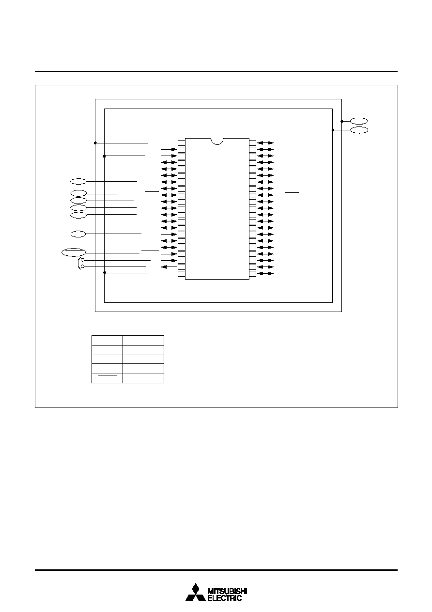
65
3850 Group (Spec. H/A)
SINGLE-CHIP 8-BIT CMOS MICROCOMPUTER
MITSUBISHI MICROCOMPUTERS
Fig. 65 Pin connection diagram in standard serial I/O mode
P4
0
/CNTR
1
P
4
1
/
I
N
T
0
P
4
2
/
I
N
T
1
P
4
3
/
I
N
T
2
/
S
C
M
P
2
A
V
S
S
P
4
4
/
I
N
T
3
/
P
W
M
V
R
E
F
P
3
1
/
A
N
1
P
3
2
/
A
N
2
P
0
0
/
S
I
N
2
P
0
4
P
0
5
P
0
6
P0
7
P
1
1
/
(
L
E
D
1
)
P
1
2
/
(
L
E
D
2
)
P
1
3
/
(
L
E
D
3
)
P
1
4
/
(
L
E
D
4
)
P1
5
/(LED
5
)
P
1
0
/
(
L
E
D
0
)
P
0
1
/
S
O
U
T
2
P
0
2
/
S
C
L
K
2
P
3
0
/
A
N
0
P
3
3
/
A
N
3
P
3
4
/
A
N
4
40
41
42
22
23
24
25
26
27
28
29
30
31
32
34
35
36
37
38
39
33
3
2
1
2
1
20
1
9
1
8
1
7
1
6
1
5
14
1
3
1
2
1
1
9
8
7
6
5
4
1
0
M
3
8
5
0
7
F
8
S
P
/
F
P
P
1
6
/
(
L
E
D
6
)
P
1
7
/
(
L
E
D
7
)
P
2
7
/
C
N
T
R
0
/
S
R
D
Y
1
P
2
6
/
S
C
L
K
P
2
5
/
T
x
D
P
2
4
/
R
x
D
C
N
V
S
S
P
2
1
/
X
C
I
N
P
2
0
/
X
C
O
U
T
RESET
X
IN
X
OUT
V
S
S
P
0
3
/
S
R
D
Y
2
P4
1
S
C
L
K
1
P2
3
/SCL
1
P
2
2
/
S
D
A
1
V
CC
V
SS
V
CC
RESET
V
P
P
2
R
X
D
T
x
D
R
x
D
B
U
S
Y
Notes 1: Connect oscillator circuit
2: Connect to Vcc when Vcc = 4.5 V to 5.5 V.
Connect to V
PP
(=4.5 V to 5.5 V) when Vcc = 2.7 V to 4.5 V.
3: It is necessary to apply Vcc only when reset is released.
Signal
Value
C
N
V
S
S
R
E
S
E
T
M
o
d
e
s
e
t
u
p
m
e
t
h
o
d
4.5 to 5.5 V
V
SS
V
CC
S
C
L
K
V
C
C
3
P
4
1
V
C
C
3
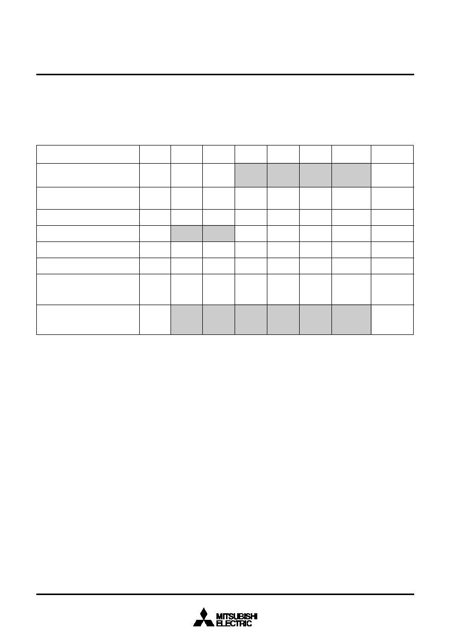
66
3850 Group (Spec. H/A)
SINGLE-CHIP 8-BIT CMOS MICROCOMPUTER
MITSUBISHI MICROCOMPUTERS
Software Commands (Standard Serial I/O
Mode)
Table 15 lists software commands. In standard serial I/O mode,
erase, program and read are controlled by transferring software
2nd byte
Address
(middle)
3rd byte
Address
(high)
4th byte
Data
output
5th byte
Data
output
6th byte
Data
output
.....
Data
output to
259th byte
Data input
to 259th
byte
FF
16
When ID is
not verified
1st byte
transfer
Notes1: Shading indicates transfer from the internal flash memory microcomputer to a programmer. All other data is transferred from an external equipment
(programmer) to the internal flash memory microcomputer.
2: SRD refers to status register data. SRD1 refers to status register 1 data.
3: All commands can be accepted when the flash memory is totally blank.
4: Address high must be "00
16
".
commands via the RxD pin. Software commands are explained
here below.
Table 15 Software commands (Standard serial I/O mode)
1
Page read
41
16
Address
(middle)
Address
(high)
Data
input
Data
input
Data
input
Not
acceptable
Not
acceptable
A7
16
D0
16
70
16
SRD
output
SRD1
output
Acceptable
50
16
Not
acceptable
F5
16
Address
(low)
Address
(middle)
Address
(high)
ID size
ID1
To ID7
Acceptable
FA
16
Data
input
To
required
number
of times
Not
acceptable
FB
16
Version
data
output
Version
data
output
Version
data
output
Version
data
output
Version
data
output
Version
data output
to 9th byte
Control command
2
Page program
3
Erase all blocks
4
Read status register
5
Clear status register
6
ID code check
7
Download function
8
Version data output function
Size
(low)
Size
(high)
Check-
sum
Acceptable
Not
acceptable

67
3850 Group (Spec. H/A)
SINGLE-CHIP 8-BIT CMOS MICROCOMPUTER
MITSUBISHI MICROCOMPUTERS
q
Read Status Register Command
This command reads status information. When the "70
16
" com-
mand code is transferred with the 1st byte, the contents of the
status register (SRD) with the 2nd byte and the contents of status
register 1 (SRD1) with the 3rd byte are read.
q
Page Read Command
This command reads the specified page (256 bytes) in the flash
memory sequentially one byte at a time. Execute the page read
command as explained here following.
(1) Transfer the "FF
16
" command code with the 1st byte.
(2) Transfer addresses A
8
to A
15
and A
16
to A
23
with the 2nd and
3rd bytes respectively.
(3) From the 4th byte onward, data (D
0
to D
7
) for the page (256
bytes) specified with addresses A
8
to A
23
will be output se-
quentially from the smallest address first synchronized with the
fall of the clock.
Fig. 66 Timing for page read
Fig. 67 Timing for reading status register
data0
data255
A
8
t
o
A
1
5
A
1
6
t
o
A
2
3
F
F
1
6
S
C
L
K
R
x
D
T
x
D
S
R
D
Y
1
(
B
U
S
Y
)
S
R
D
o
u
t
p
u
t
S
R
D
1
o
u
t
p
u
t
S
C
L
K
R
x
D
T
x
D
S
R
D
Y
1
(
B
U
S
Y
)
7
0
1
6

68
3850 Group (Spec. H/A)
SINGLE-CHIP 8-BIT CMOS MICROCOMPUTER
MITSUBISHI MICROCOMPUTERS
Fig. 68 Timing for clear status register
q
Clear Status Register Command
This command clears the bits (SR4, SR5) which are set when the
status register operation ends in error. When the "50
16
" command
code is sent with the 1st byte, the aforementioned bits are
cleared. When the clear status register operation ends, the S
RDY1
(BUSY) signal changes from "H" to "L" level.
q
Page Program Command
This command writes the specified page (256 bytes) in the flash
memory sequentially one byte at a time. Execute the page pro-
gram command as explained here following.
(1) Transfer the "41
16
" command code with the 1st byte.
(2) Transfer addresses A
8
to A
15
and A
16
to A
23
("00
16
") with the
2nd and 3rd bytes respectively.
(3) From the 4th byte onward, as write data (D
0
to D
7
) for the
page (256 bytes) specified with addresses A
8
to A
23
is input
sequentially from the smallest address first, that page is auto-
matically written.
When reception setup for the next 256 bytes ends, the S
RDY1
(BUSY) signal changes from "H" to "L" level. The result of the
page program can be known by reading the status register. For
more information, see the section on the status register.
Fig. 69 Timing for page program
S
C
L
K
R
x
D
T
x
D
S
R
D
Y
1
(
B
U
S
Y
)
50
16
A
8
t
o
A
1
5
A
1
6
t
o
A
2
3
4
1
1
6
d
a
t
a
0
d
a
t
a
2
5
5
S
C
L
K
R
x
D
T
x
D
S
R
D
Y
1
(
B
U
S
Y
)
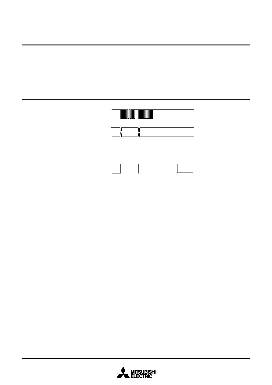
69
3850 Group (Spec. H/A)
SINGLE-CHIP 8-BIT CMOS MICROCOMPUTER
MITSUBISHI MICROCOMPUTERS
q
Erase All Blocks Command
This command erases the contents of all blocks. Execute the
erase all blocks command as explained here following.
(1) Transfer the "A7
16
" command code with the 1st byte.
(2) Transfer the verify command code "D0
16
" with the 2nd byte.
With the verify command code, the erase operation will start
and continue for all blocks in the flash memory.
When erase all blocks end, the S
RDY1
(BUSY) signal changes
from "H" to "L" level. The result of the erase operation can be
known by reading the status register.
Fig. 70 Timing for erase all blocks
A7
16
D
0
1
6
S
C
L
K
R
x
D
T
x
D
S
R
D
Y
1
(
B
U
S
Y
)
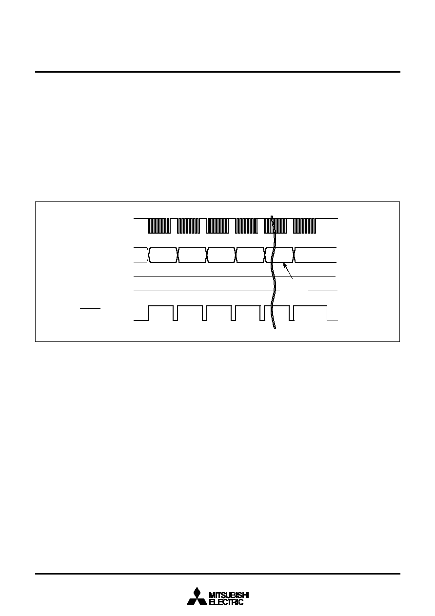
70
3850 Group (Spec. H/A)
SINGLE-CHIP 8-BIT CMOS MICROCOMPUTER
MITSUBISHI MICROCOMPUTERS
q
Download Command
This command downloads a program to the RAM for execution.
Execute the download command as explained here following.
(1) Transfer the "FA
16
" command code with the 1st byte.
(2) Transfer the program size with the 2nd and 3rd bytes.
(3) Transfer the check sum with the 4th byte. The check sum is
added to all data sent with the 5th byte onward.
(4) The program to execute is sent with the 5th byte onward.
When all data has been transmitted, if the check sum matches,
the downloaded program is executed. The size of the program will
vary according to the internal RAM.
Fig. 71 Timing for download
FA
16
Program
data
P
r
o
g
r
a
m
d
a
t
a
D
a
t
a
s
i
z
e
(
l
o
w
)
C
h
e
c
k
s
u
m
S
C
L
K
R
x
D
T
x
D
S
R
D
Y
1
(
B
U
S
Y
)
D
a
t
a
s
i
z
e
(
h
i
g
h
)
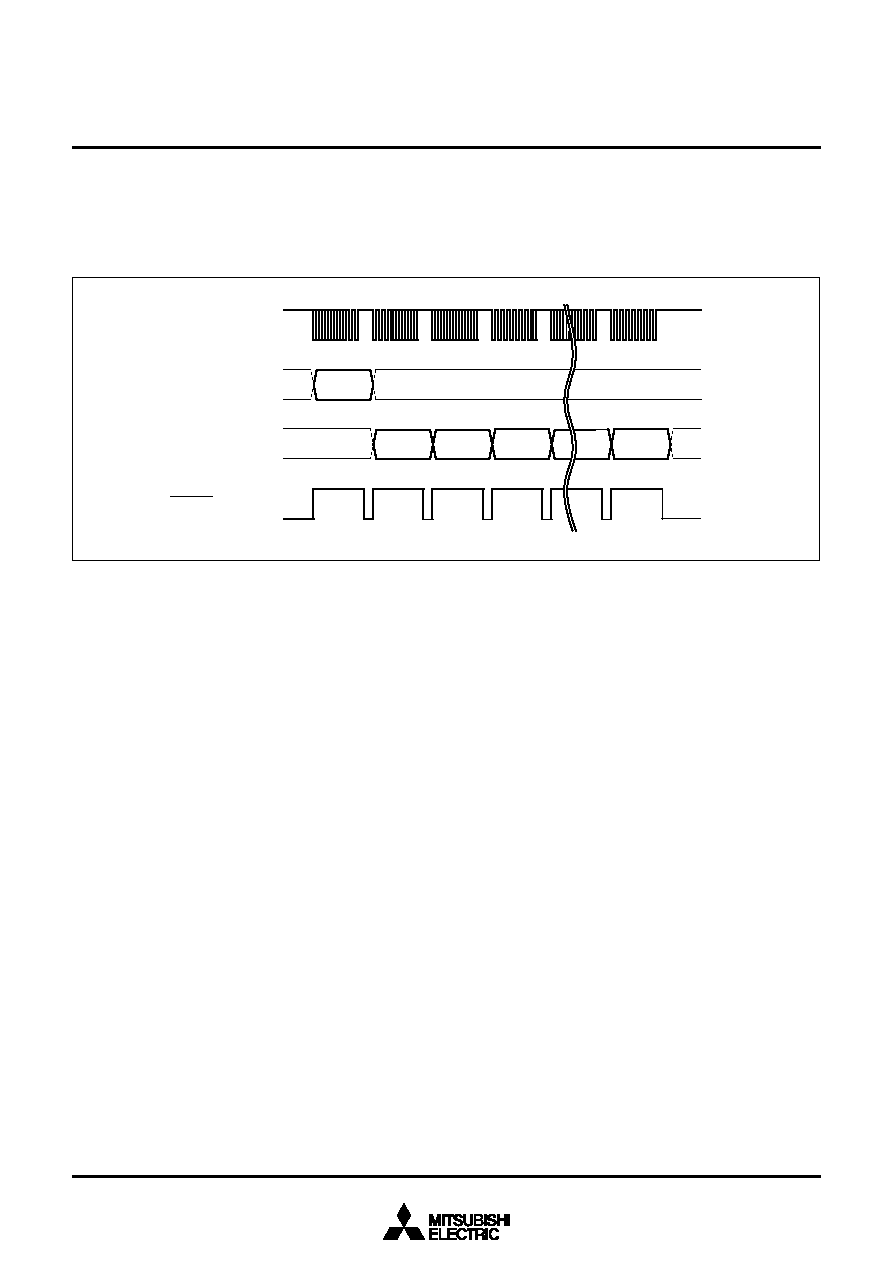
71
3850 Group (Spec. H/A)
SINGLE-CHIP 8-BIT CMOS MICROCOMPUTER
MITSUBISHI MICROCOMPUTERS
q
Version Information Output Command
This command outputs the version information of the control pro-
gram stored in the Boot ROM area. Execute the version
information output command as explained here following.
(1) Transfer the "FB
16
" command code with the 1st byte.
(2) The version information will be output from the 2nd byte on-
ward.
This data is composed of 8 ASCII code characters.
Fig. 72 Timing for version information output
F
B
1
6
`
X
'
`V
'
`E'
`
R
'
S
C
L
K
R
x
D
T
x
D
S
R
D
Y
1
(
B
U
S
Y
)

72
3850 Group (Spec. H/A)
SINGLE-CHIP 8-BIT CMOS MICROCOMPUTER
MITSUBISHI MICROCOMPUTERS
q
ID Check
This command checks the ID code. Execute the boot ID check
command as explained here following.
q
ID Code
When the flash memory is not blank, the ID code sent from the se-
rial programmer and the ID code written in the flash memory are
compared to see if they match. If the codes do not match, the
command sent from the serial programmer is not accepted. An ID
code contains 8 bits of data. Area is, from the 1st byte, addresses
FFD4
16
to FFDA
16
. Write a program into the flash memory, which
already has the ID code set for these addresses.
Fig. 73 Timing for ID check
Fig. 74 ID code storage addresses
(1) Transfer the "F5
16
" command code with the 1st byte.
(2) Transfer addresses A
0
to A
7
, A
8
to A
15
and A
16
to A
23
("00
16
")
of the 1st byte of the ID code with the 2nd, 3rd, and 4th bytes
respectively.
(3) Transfer the number of data sets of the ID code with the 5th
byte.
(4) Transfer the ID code with the 6th byte onward, starting with the
1st byte of the code.
I
D
s
i
z
e
I
D
1
I
D
7
F
5
1
6
D
4
1
6
F
F
1
6
0
0
1
6
S
C
L
K
R
x
D
T
x
D
S
R
D
Y
1
(
B
U
S
Y
)
R
O
M
c
o
d
e
p
r
o
t
e
c
t
c
o
n
t
r
o
l
ID7
I
D
6
I
D
5
I
D
4
ID3
ID2
I
D
1
FFDB
16
FFDA
16
FFD9
16
F
F
D
8
1
6
F
F
D
7
1
6
F
F
D
6
1
6
F
F
D
5
1
6
F
F
D
4
1
6
Address
I
n
t
e
r
r
u
p
t
v
e
c
t
o
r
a
r
e
a
73
3850 Group (Spec. H/A)
SINGLE-CHIP 8-BIT CMOS MICROCOMPUTER
MITSUBISHI MICROCOMPUTERS
q
Status Register (SRD)
The status register indicates operating status of the flash memory
and status such as whether an erase operation or a program
ended successfully or in error. It can be read by writing the read
status register command (70
16
). Also, the status register is
cleared by writing the clear status register command (50
16
).
Table 16 lists the definition of each status register bit. After releas-
ing the reset, the status register becomes "80
16
".
∑Sequencer status (SR7)
The sequencer status indicates the operating status of the flash
memory.
After power-on and recover from deep power down mode, the se-
quencer status is set to "1" (ready).
This status bit is set to "0" (busy) during write or erase operation
and is set to "1" upon completion of these operations.
∑Erase status (SR5)
The erase status indicates the operating status of erase operation.
If an erase error occurs, it is set to "1". When the erase status is
cleared, it is set to "0".
∑Program status (SR4)
The program status indicates the operating status of write opera-
tion. If a program error occurs, it is set to "1". When the program
status is cleared, it is set to "0".
SRD0 bits
SR7 (bit7)
SR6 (bit6)
SR5 (bit5)
SR4 (bit4)
SR3 (bit3)
SR2 (bit2)
SR1 (bit1)
SR0 (bit0)
Definition
"1"
"0"
Table 16 Definition of each bit of status register (SRD)
Status name
Sequencer status
Reserved
Erase status
Program status
Reserved
Reserved
Reserved
Reserved
Ready
-
Terminated in error
Terminated in error
-
-
-
-
Busy
-
Terminated normally
Terminated normally
-
-
-
-

74
3850 Group (Spec. H/A)
SINGLE-CHIP 8-BIT CMOS MICROCOMPUTER
MITSUBISHI MICROCOMPUTERS
q
Status Register 1 (SRD1)
The status register 1 indicates the status of serial communica-
tions, results from ID checks and results from check sum
comparisons. It can be read after the status register (SRD) by writ-
ing the read status register command (70
16
). Also, status register
1 is cleared by writing the clear status register command (50
16
).
Table 17 lists the definition of each status register 1 bit. This regis-
ter becomes "00
16
" when power is turned on and the flag status is
maintained even after the reset.
Table 17 Definition of each bit of status register 1 (SRD1)
00
Not verified
01
Verification mismatch
10
Reserved
11
Verified
SR15 (bit7)
SR14 (bit6)
SR13 (bit5)
SR12 (bit4)
SR11 (bit3)
SR10 (bit2)
SR9 (bit1)
SR8 (bit0)
Boot update completed bit
Reserved
Reserved
Checksum match bit
ID check completed bits
Data reception time out
Reserved
"1"
Update completed
-
-
Match
Time out
-
"0"
Not Update
-
-
Mismatch
Normal operation
-
Definition
SRD1 bits
Status name
∑Boot update completed bit (SR15)
This flag indicates whether the control program was downloaded
to the RAM or not, using the download function.
∑Check sum consistency bit (SR12)
This flag indicates whether the check sum matches or not when a
program, is downloaded for execution using the download func-
tion.
∑ID check completed bits (SR11 and SR10)
These flags indicate the result of ID checks. Some commands
cannot be accepted without an ID code check.
∑Data reception time out (SR9)
This flag indicates when a time out error is generated during data
reception. If this flag is attached during data reception, the re-
ceived data is discarded and the MCU returns to the command
wait state.
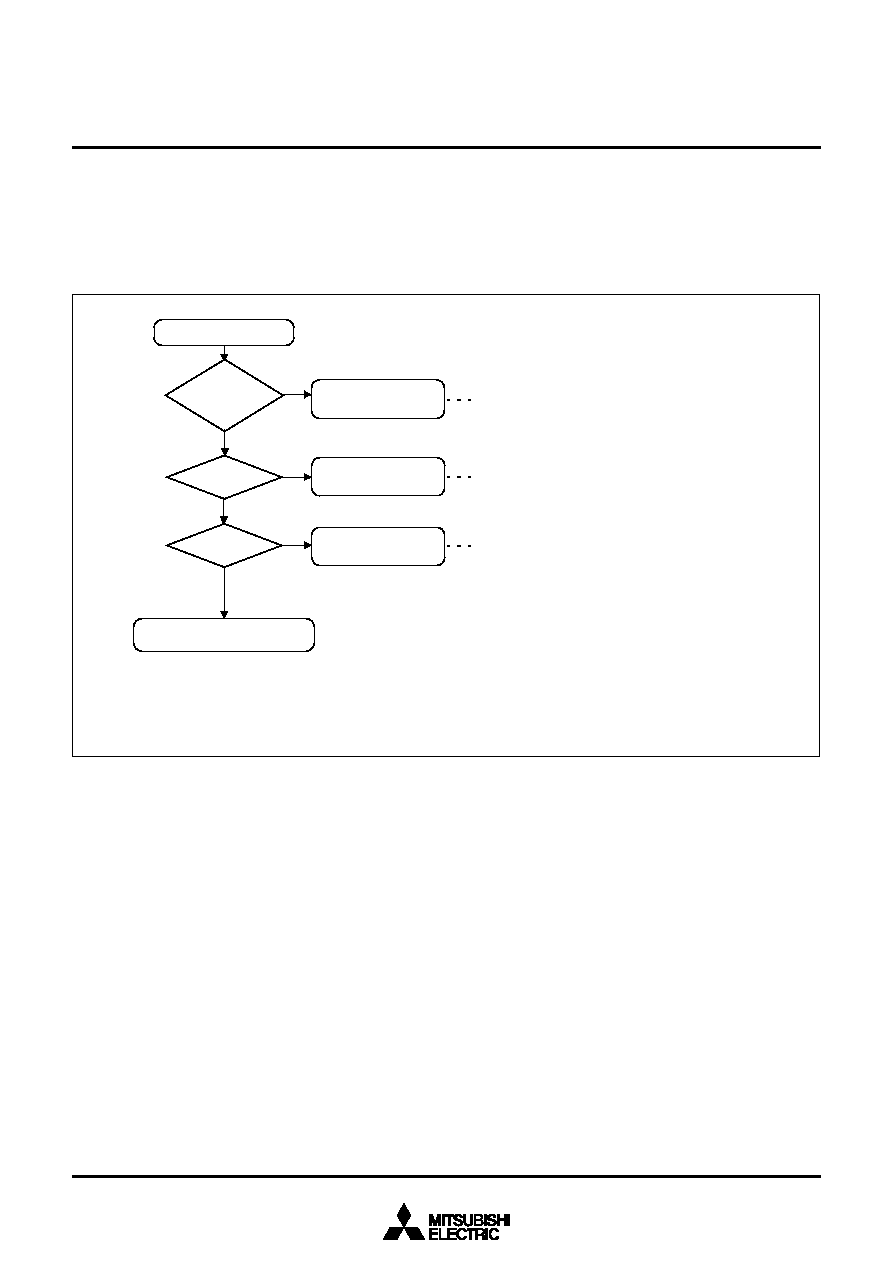
75
3850 Group (Spec. H/A)
SINGLE-CHIP 8-BIT CMOS MICROCOMPUTER
MITSUBISHI MICROCOMPUTERS
Full Status Check
Results from executed erase and program operations can be
known by running a full status check. Figure 75 shows a flowchart
of the full status check and explains how to remedy errors which
occur.
Fig. 75 Full status check flowchart and remedial procedure for errors
Read status register
S
R
4
=
1
a
n
d
S
R5
=
1
?
NO
Y
E
S
SR5 = 0 ?
Y
E
S
Er
a
s
e
e
r
r
o
r
NO
SR4 = 0 ?
Y
E
S
N
O
Command
sequence error
Program error
End (Erase, program)
E
x
e
c
u
t
e
t
h
e
c
l
e
a
r
s
t
a
t
u
s
r
e
g
i
s
t
e
r
c
o
m
m
a
n
d
(
5
0
1
6
)
t
o
c
l
e
a
r
t
h
e
s
t
a
t
u
s
r
e
g
i
s
t
e
r
.
T
r
y
p
e
r
f
o
r
m
i
n
g
t
h
e
o
p
e
r
a
t
i
o
n
o
n
e
m
o
r
e
t
i
m
e
a
f
t
e
r
c
o
n
f
i
r
m
i
n
g
t
h
a
t
t
h
e
c
o
m
m
a
n
d
i
s
e
n
t
e
r
e
d
c
o
r
r
e
c
t
l
y
.
S
h
o
u
l
d
a
n
e
r
a
s
e
e
r
r
o
r
o
c
c
u
r
,
t
h
e
b
l
o
c
k
i
n
e
r
r
o
r
c
a
n
n
o
t
b
e
u
s
e
d
.
Note: When one of SR5 to SR4 is set to "1" , none of the program, erase all blocks
commands is accepted. Execute the clear status register command (50
16
) before
executing these commands.
S
h
o
u
l
d
a
p
r
o
g
r
a
m
e
r
r
o
r
o
c
c
u
r
,
t
h
e
b
l
o
c
k
i
n
e
r
r
o
r
c
a
n
n
o
t
b
e
u
s
e
d
.
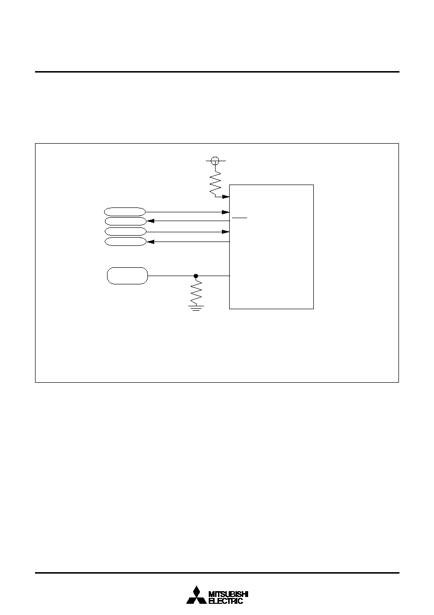
76
3850 Group (Spec. H/A)
SINGLE-CHIP 8-BIT CMOS MICROCOMPUTER
MITSUBISHI MICROCOMPUTERS
Example Circuit Application for Standard
Serial I/O Mode
Figure 76 shows a circuit application for the standard serial I/O
mode. Control pins will vary according to a programmer, therefore
see a programmer manual for more information.
Fig. 76 Example circuit application for standard serial I/O mode
S
RDY1
(BUSY)
S
C
L
K
R
X
D
T
X
D
CNVss
C
l
o
c
k
i
n
p
u
t
B
U
S
Y
o
u
t
p
u
t
D
a
t
a
i
n
p
u
t
D
a
t
a
o
u
t
p
u
t
M
3
8
5
0
7
F
8
Notes 1: Control pins and external circuitry will vary according to peripheral unit. For more
information, see the peripheral unit manual.
2: In this example, the Vpp power supply is supplied from an external source (writer). To use
the user's power source, connect to 4.5 V to 5.5 V.
3: It is necessary to apply Vcc to S
CLK
pin only when reset is released.
V
P
P
p
o
w
e
r
s
o
u
r
c
e
i
n
p
u
t
P
4
1
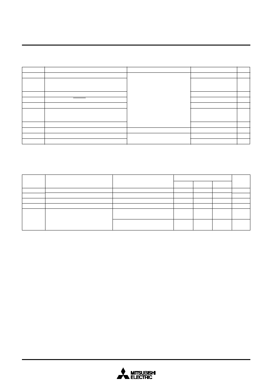
77
3850 Group (Spec. H/A)
SINGLE-CHIP 8-BIT CMOS MICROCOMPUTER
MITSUBISHI MICROCOMPUTERS
Table 19 Flash memory mode Electrical characteristics
(Ta = 25
o
C, V
CC
= 4.5 to 5.5V unless otherwise noted)
Flash memory Electrical characteristics
Limits
Parameter
Min.
Typ.
Max.
Symbol
Unit
Conditions
I
PP1
I
PP2
I
PP3
V
PP
V
CC
4.5
Table 18 Absolute maximum ratings
Power source voltage
Input voltage
P0
0
≠P0
7
, P1
0
≠P1
7
, P2
0
, P2
1,
P2
4
≠P2
7
, P3
0
≠P3
4
, P4
0
≠P4
4
,
V
REF
Input voltage
P2
2
, P2
3
Input voltage
RESET, X
IN
Input voltage
CNV
SS
Output voltage P0
0
≠P0
7
, P1
0
≠P1
7
, P2
0
, P2
1,
P2
4
≠P2
7
, P3
0
≠P3
4
, P4
0
≠P4
4
,
X
OUT
Output voltage P2
2
, P2
3
Power dissipation
Operating temperature
Storage temperature
V
CC
V
I
V
I
V
I
V
I
V
O
V
O
P
d
T
opr
T
stg
Symbol
Parameter
Conditions
Ratings
≠0.3 to 6.5
≠0.3 to V
CC
+0.3
≠0.3 to 5.8
≠0.3 to V
CC
+0.3
≠0.3 to 6.5
≠0.3 to V
CC
+0.3
≠0.3 to 5.8
1000 (Note)
25±5
≠40 to 125
V
V
V
V
V
V
V
mW
∞C
∞C
Unit
T
a
= 25 ∞C
All voltages are based on V
SS
.
Output transistors are cut off.
Note:
The rating becomes 300 mW at the 42P2R-A/E package.
4.5
3.0
5.5
3.6
V
V
V
PP
power source current (read)
V
PP
power source current (program)
V
PP
power source current (erase)
V
PP
power source voltage
V
CC
power source voltage
100
60
30
5.5
µ
A
mA
mA
V
V
PP
= V
CC
V
PP
= V
CC
V
PP
= V
CC
Microcomputer mode operation at
V
CC
= 2.7 to 5.5V
Microcomputer mode operation at
V
CC
= 2.7 to 3.6V

78
SINGLE-CHIP 8-BIT CMOS MICROCOMPUTER
MITSUBISHI MICROCOMPUTERS
NOTES ON PROGRAMMING
Processor Status Register
The contents of the processor status register (PS) after a reset are
undefined, except for the interrupt disable flag (I) which is "1." Af-
ter a reset, initialize flags which affect program execution. In
particular, it is essential to initialize the index X mode (T) and the
decimal mode (D) flags because of their effect on calculations.
Interrupts
The contents of the interrupt request bits do not change immedi-
ately after they have been written. After writing to an interrupt
request register, execute at least one instruction before perform-
ing a BBC or BBS instruction.
Decimal Calculations
∑ To calculate in decimal notation, set the decimal mode flag (D)
to "1", then execute an ADC or SBC instruction. After executing
an ADC or SBC instruction, execute at least one instruction be-
fore executing a SEC, CLC, or CLD instruction.
∑ In decimal mode, the values of the negative (N), overflow (V),
and zero (Z) flags are invalid.
Timers
If a value n (between 0 and 255) is written to a timer latch, the fre-
quency division ratio is 1/(n+1).
Multiplication and Division Instructions
∑ The index X mode (T) and the decimal mode (D) flags do not af-
fect the MUL and DIV instruction.
∑ The execution of these instructions does not change the con-
tents of the processor status register.
Ports
The contents of the port direction registers cannot be read. The
following cannot be used:
∑ The data transfer instruction (LDA, etc.)
∑ The operation instruction when the index X mode flag (T) is "1"
∑ The addressing mode which uses the value of a direction regis-
ter as an index
∑ The bit-test instruction (BBC or BBS, etc.) to a direction register
∑ The read-modify-write instructions (ROR, CLB, or SEB, etc.) to
a direction register.
Use instructions such as LDM and STA, etc., to set the port direc-
tion registers.
Serial I/O
In clock synchronous serial I/O, if the receive side is using an ex-
ternal clock and it is to output the S
RDY1
signal, set the transmit
enable bit, the receive enable bit, and the S
RDY1
output enable bit
to "1."
Serial I/O1 continues to output the final bit from the T
X
D pin after
transmission is completed.
S
OUT2
pin for serial I/O2 goes to high impedance after transmis-
sion is completed.
When an external clock is used as synchronous clock in serial I/
O1 or serial I/O2, write transmission data to the transmit buffer
register or serial I/O2 register while the transfer clock is "H."
A-D Converter
The comparator uses capacitive coupling amplifier whose charge
will be lost if the clock frequency is too low.
Therefore, make sure that f(X
IN
) in the middle/high-speed mode is
at least on 500 kHz during an A-D conversion.
Do not execute the STP instruction during an A-D conversion.
Instruction Execution Time
The instruction execution time is obtained by multiplying the fre-
quency of the internal clock
by the number of cycles needed to
execute an instruction.
The number of cycles required to execute an instruction is shown
in the list of machine instructions.
The frequency of the internal clock
is half of the X
IN
frequency in
high-speed mode.
NOTES ON USAGE
Differences among 3850 group (standard),
3850 group (spec. H), and 3850 group (spec.
A)
(1) The absolute maximum ratings of 3850 group (spec. H/A) is
smaller than that of 3850 group (standard).
∑Power source voltage Vcc = ≠0.3 to 6.5 V
∑CNVss input voltage V
I
= ≠0.3 to Vcc +0.3 V
(2) The oscillation circuit constants of X
IN
-X
OUT
, X
CIN
-X
COUT
may
be some differences between 3850 group (standard) and 3850
group (spec. H/A).
(3) Do not write any data to the reserved area and the reserved
bit. (Do not change the contents after rest.)
(4) Fix bit 3 of the CPU mode register to "1".
(5) Be sure to perform the termination of unused pins.
Handling of Source Pins
In order to avoid a latch-up occurrence, connect a capacitor suit-
able for high frequencies as bypass capacitor between power
source pin (V
CC
pin) and GND pin (V
SS
pin) and between power
source pin (V
CC
pin) and analog power source input pin (AV
SS
pin). Besides, connect the capacitor to as close as possible. For
bypass capacitor which should not be located too far from the pins
to be connected, a ceramic capacitor of 0.01
µ
F≠0.1
µ
F is recom-
mended.
EPROM Version/One Time PROM Version/
Flash Memory Version
The CNVss pin is connected to the internal memory circuit block
by a low-ohmic resistance, since it has the multiplexed function to
be a programmable power source pin (V
PP
pin) as well.
To improve the noise reduction, connect a track between CNVss
pin and Vss pin or Vcc pin with 1 to 10 k
resistance.
The mask ROM version track of CNVss pin has no operational in-
terference even if it is connected to Vss pin or Vcc pin via a
resistor.
3850 Group (Spec. H/A)

79
SINGLE-CHIP 8-BIT CMOS MICROCOMPUTER
MITSUBISHI MICROCOMPUTERS
Electric Characteristic Differences Among
Mask ROM, Flash Memory, and One Time
PROM Version MCUs
There are differences in electric characteristics, operation margin,
noise immunity, and noise radiation among mask ROM, flash
memory, and One Time PROM version MCUs due to the differ-
ences in the manufacturing processes.
When manufacturing an application system with the flash memory,
One Time PROM version and then switching to use of the mask
ROM version, perform sufficient evaluations for the commercial
samples of the mask ROM version.
DATA REQUIRED FOR MASK ORDERS
The following are necessary when ordering a mask ROM produc-
tion:
1. Mask ROM Order Confirmation Form
2. Mark Specification Form
3. Data to be written to ROM, in EPROM form (three identical cop-
ies) or one floppy disk.
DATA REQUIRED FOR One Time PROM
PROGRAMMING ORDERS
The following are necessary when ordering a PROM programming
service:
1. ROM Programming Confirmation Form
2. Mark Specification Form
(only special mark with customer's
trade mark logo)
3. Data to be programmed to PROM, in EPROM form (three iden-
tical copies) or one floppy disk.
For the mask ROM confirmation and the mark specifications, re-
fer to the "Mitsubishi MCU Technical Information" Homepage
(http://www.infomicom.maec.co.jp/indexe.htm).
ROM PROGRAMMING METHOD
The built-in PROM of the blank One Time PROM version and buit-
in EPROM version can be read or programmed with a
general-purpose PROM programmer using a special programming
adapter. Set the address of PROM programmer in the user ROM
area.
Table 20 Programming adapter
Package
42P4B, 42S1B
42P2R-A/E
Name of Programming Adapter
PCA4738S-42A
PCA4738F-42A
The PROM of the blank One Time PROM version is not tested or
screened in the assembly process and following processes. To en-
sure proper operation after programming, the procedure shown in
Figure 77 is recommended to verify programming.
Fig. 77 Programming and testing of One Time PROM version
3850 Group (Spec. H/A)
Programming with PROM
programmer
Screening (Caution)
(150 ∞C for 40 hours)
V
e
r
i
f
i
c
a
t
i
o
n
w
i
t
h
P
R
O
M
p
r
o
g
r
a
m
m
e
r
F
u
n
c
t
i
o
n
a
l
c
h
e
c
k
i
n
t
a
r
g
e
t
d
e
v
i
c
e
The screening temperature is far higher
than the storage temperature. Never
expose to 150 ∞C exceeding 100 hours.
Caution :

80
SINGLE-CHIP 8-BIT CMOS MICROCOMPUTER
MITSUBISHI MICROCOMPUTERS
3850 Group (Spec. H/A)
Electrical characteristics
Absolute maximum ratings
Table 21 Absolute maximum ratings
Power source voltage
Input voltage
P0
0
≠P0
7
, P1
0
≠P1
7
, P2
0
, P2
1,
P2
4
≠P2
7
, P3
0
≠P3
4
, P4
0
≠P4
4
,
V
REF
Input voltage
P2
2
, P2
3
Input voltage
RESET, X
IN
Input voltage
CNV
SS
Output voltage P0
0
≠P0
7
, P1
0
≠P1
7
, P2
0
, P2
1,
P2
4
≠P2
7
, P3
0
≠P3
4
, P4
0
≠P4
4
,
X
OUT
Output voltage P2
2
, P2
3
Power dissipation
Operating temperature
Storage temperature
V
CC
V
I
V
I
V
I
V
I
V
O
V
O
P
d
T
opr
T
stg
Symbol
Parameter
Conditions
Ratings
≠0.3 to 6.5
≠0.3 to V
CC
+0.3
≠0.3 to 5.8
≠0.3 to V
CC
+0.3
≠0.3 to V
CC
+0.3
≠0.3 to V
CC
+0.3
≠0.3 to 5.8
1000 (Note)
≠20 to 85
≠40 to 125
V
V
V
V
V
V
V
mW
∞C
∞C
Unit
T
a
= 25 ∞C
All voltages are based on V
SS
.
Output transistors are cut off.
Note : The rating becomes 300mW at the 42P2R-A/E package.
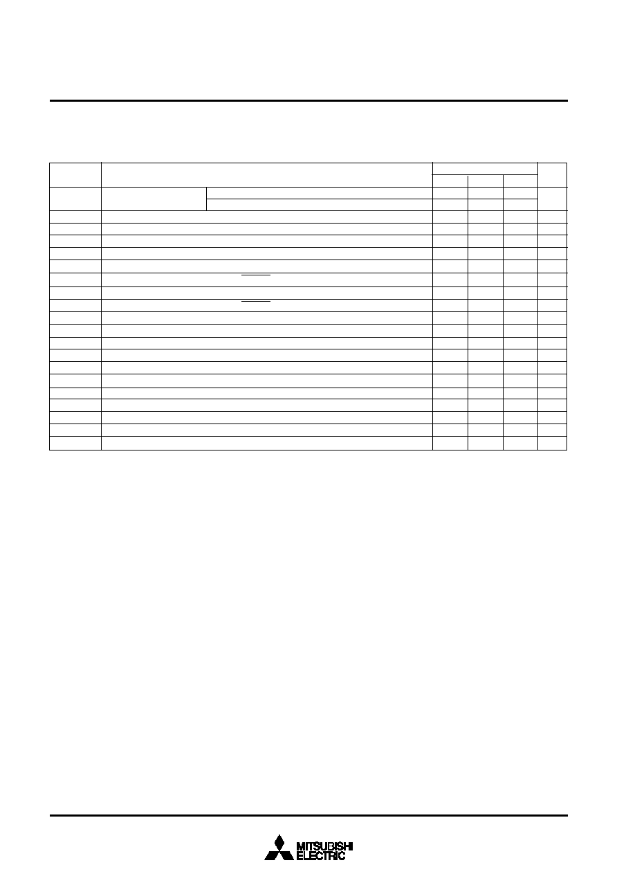
81
SINGLE-CHIP 8-BIT CMOS MICROCOMPUTER
MITSUBISHI MICROCOMPUTERS
Table 22 Recommended operating conditions (1) (spec. H)
(V
CC
= 2.7 to 5.5 V, T
a
= ≠20 to 85 ∞C, unless otherwise noted)
Recommended operating conditions
V
CC
V
SS
V
REF
AV
SS
V
IA
V
IH
V
IH
V
IL
V
IL
V
IL
5.5
5.5
V
CC
V
CC
V
CC
V
CC
0.2V
CC
0.2V
CC
0.16V
CC
Power source voltage
Power source voltage
A-D convert reference voltage
Analog power source voltage
Analog input voltage
AN
0
≠AN
4
"H" input voltage
P0
0
≠P0
7
, P1
0
≠P1
7
, P2
0
≠P2
7
, P3
0
≠P3
4
, P4
0
≠P4
4
"H" input voltage
RESET, X
IN
, CNV
SS
"L" input voltage
P0
0
≠P0
7
, P1
0
≠P1
7
, P2
0
≠P2
7
, P3
0
≠P3
4
, P4
0
≠P4
4
"L" input voltage
RESET, CNV
SS
"L" input voltage
X
IN
Symbol
Parameter
Limits
Min.
Unit
4.0
2.7
2.0
AV
SS
0.8V
CC
0.8V
CC
0
0
0
5.0
5.0
0
0
Typ.
Max.
≠80
≠80
80
120
80
≠40
≠40
40
60
40
"H" total peak output current (Note) P0
0
≠P0
7
, P1
0
≠P1
7
, P3
0
≠P3
4
"H" total peak output current (Note) P2
0
, P2
1
, P2
4
≠P2
7
, P4
0
≠P4
4
"L" total peak output current (Note) P0
0
≠P0
7
, P3
0
≠P3
4
"L" total peak output current (Note) P1
0
≠P1
7
"L" total peak output current (Note) P2
0
≠P2
7
,P4
0
≠P4
4
"H" total average output current (Note)
P0
0
≠P0
7
, P1
0
≠P1
7
, P3
0
≠P3
4
"H" total average output current (Note)
P2
0
, P2
1
, P2
4
≠P2
7
, P4
0
≠P4
4
"L" total average output current (Note)
P0
0
≠P0
7
, P3
0
≠P3
4
"L" total average output current (Note)
P1
0
≠P1
7
"L" total average output current (Note)
P2
0
≠P2
7
,P4
0
≠P4
4
I
OH(peak)
I
OH(peak)
I
OL(peak)
I
OL(peak)
I
OL(peak)
I
OH(avg)
I
OH(avg)
I
OL(avg)
I
OL(avg)
I
OL(avg)
mA
mA
mA
mA
mA
mA
mA
mA
mA
mA
Note : The total output current is the sum of all the currents flowing through all the applicable ports. The total average current is an average value measured
over 100 ms. The total peak current is the peak value of all the currents.
V
V
V
V
V
V
V
V
V
V
8 MHz (high-speed mode)
8 MHz (middle-speed mode), 4 MHz (high-speed mode)
3850 Group (Spec. H)

82
SINGLE-CHIP 8-BIT CMOS MICROCOMPUTER
MITSUBISHI MICROCOMPUTERS
Table 23 Recommended operating conditions (1) (spec. A)
(V
CC
= 2.7 to 5.5 V, T
a
= ≠20 to 85 ∞C, unless otherwise noted)
Recommended operating conditions
V
CC
V
SS
V
REF
AV
SS
V
IA
V
IH
V
IH
V
IL
V
IL
V
IL
I
OH(peak)
I
OH(peak)
I
OL(peak)
I
OL(peak)
I
OL(peak)
I
OH(avg)
I
OH(avg)
I
OL(avg)
I
OL(avg)
I
OL(avg)
5.5
5.5
V
CC
V
CC
V
CC
V
CC
0.2V
CC
0.2V
CC
0.16V
CC
≠80
≠80
80
120
80
≠40
≠40
40
60
40
Power source voltage
Power source voltage
A-D convert reference voltage
Analog power source voltage
Analog input voltage
AN
0
≠AN
8
"H" input voltage
P0
0
≠P0
7
, P1
0
≠P1
7
, P2
0
≠P2
7
, P3
0
≠P3
4
, P4
0
≠P4
4
"H" input voltage
RESET, X
IN
, CNV
SS
"L" input voltage
P0
0
≠P0
7
, P1
0
≠P1
7
, P2
0
≠P2
7
, P3
0
≠P3
4
, P4
0
≠P4
4
"L" input voltage
RESET, CNV
SS
"L" input voltage
X
IN
"H" total peak output current (Note) P0
0
≠P0
7
, P1
0
≠P1
7
, P3
0
≠P3
4
"H" total peak output current (Note) P2
0
, P2
1
, P2
4
≠P2
7
, P4
0
≠P4
4
"L" total peak output current (Note) P0
0
≠P0
7
, P3
0
≠P3
4
"L" total peak output current (Note) P1
0
≠P1
7
"L" total peak output current(Note) P2
0
≠P2
7
,P4
0
≠P4
4
"H" total average output current (Note)
P0
0
≠P0
7
, P1
0
≠P1
7
, P3
0
≠P3
4
"H" total average output current (Note)
P2
0
, P2
1
, P2
4
≠P2
7
, P4
0
≠P4
4
"L" total average output current (Note)
P0
0
≠P0
7
, P3
0
≠P3
4
"L" total average output current (Note)
P1
0
≠P1
7
"L" total average output current (Note)
P2
0
≠P2
7
,P4
0
≠P4
4
Symbol
Parameter
Limits
Min.
Unit
4.0
2.7
2.0
AV
SS
0.8V
CC
0.8V
CC
0
0
0
5.0
5.0
0
0
Typ.
Max.
Note : The total output current is the sum of all the currents flowing through all the applicable ports. The total average current is an average value measured
over 100 ms. The total peak current is the peak value of all the currents.
V
V
V
V
V
V
V
V
V
V
mA
mA
mA
mA
mA
mA
mA
mA
mA
mA
12.5 MHz (high-speed mode)
12.5 MHz (middle-speed mode), 6 MHz (high-speed mode)
32 kHz (low-speed mode)
3850 Group (Spec. A)
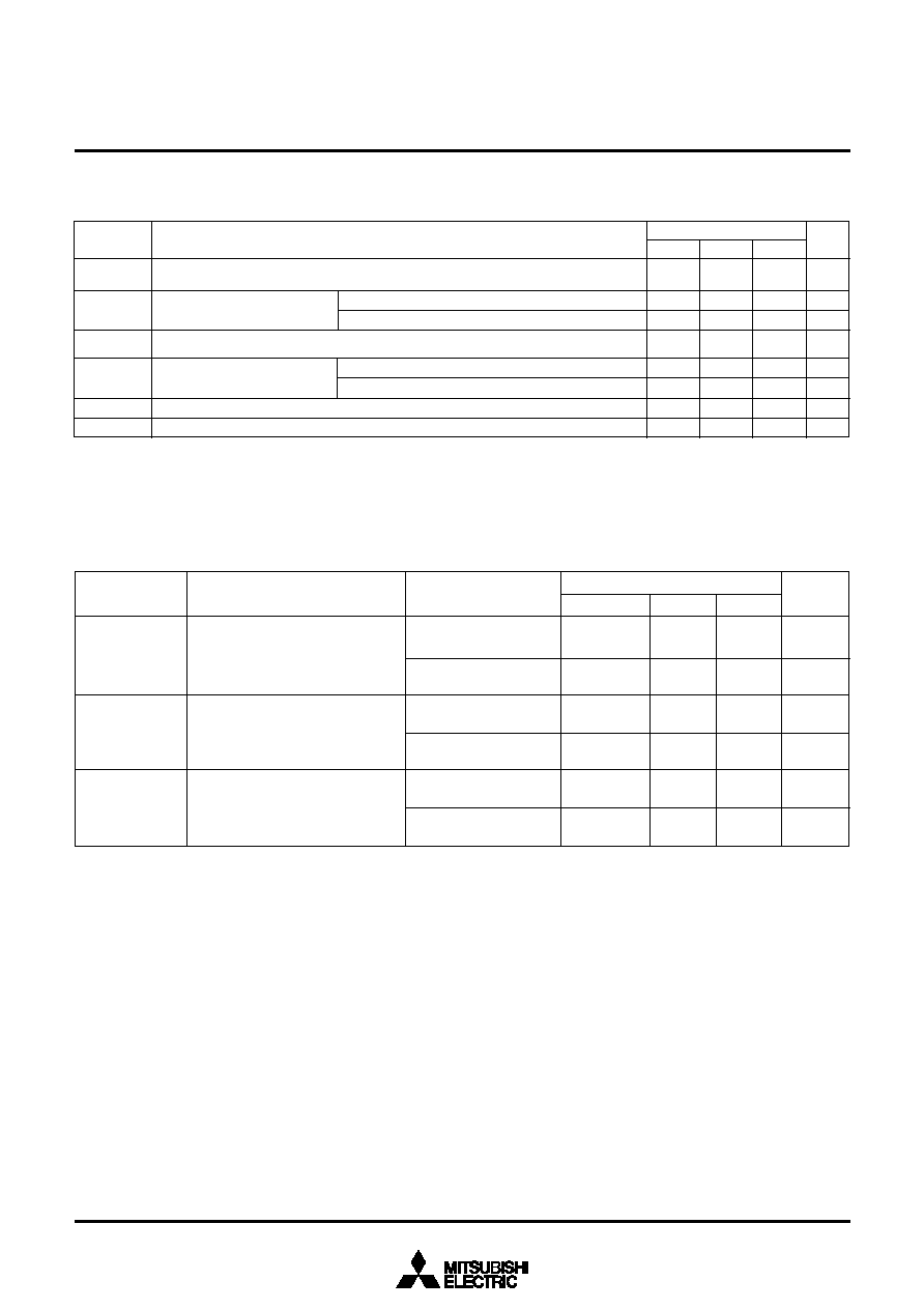
83
SINGLE-CHIP 8-BIT CMOS MICROCOMPUTER
MITSUBISHI MICROCOMPUTERS
Table 24 Recommended operating conditions (2) (spec. H)
(V
CC
= 2.7 to 5.5 V, Ta = ≠20 to 85 ∞C, unless otherwise noted)
≠10
10
20
≠5
5
15
8
4
"H" peak output current
P0
0
≠P0
7
, P1
0
≠P1
7
, P2
0
, P2
1
, P2
4
≠P2
7
, P3
0
≠P3
4
,
P4
0
≠P4
4
(Note 1)
"L" peak output current (Note 1)
P0
0
≠P0
7
, P2
0
≠P2
7
, P3
0
≠P3
4
, P4
0
≠P4
4
P1
0
≠P1
7
"H" average output current
P0
0
≠P0
7
, P1
0
≠P1
7
, P2
0
, P2
1
, P2
4
≠P2
7
, P3
0
≠P3
4
,
P4
0
≠P4
4
(Note 2)
"L" average output current (Note 2) P0
0
≠P0
7
, P2
0
≠P2
7
, P3
0
≠P3
4
, P4
0
≠P4
4
P1
0
≠P1
7
Internal clock oscillation frequency (V
CC
= 4.0 to 5.5V) (Note 3)
Internal clock oscillation frequency (V
CC
= 2.7 to 5.5V) (Note 3)
I
OH(peak)
I
OL(peak)
I
OH(avg)
I
OL(avg)
f(X
IN
)
f(X
IN
)
Symbol
Parameter
Limits
Min.
mA
mA
mA
mA
mA
mA
MHz
MHz
Unit
Typ.
Max.
Notes 1: The peak output current is the peak current flowing in each port.
2: The average output current I
OL
(avg), I
OH
(avg) are average value measured over 100 ms.
3: When the oscillation frequency has a duty cycle of 50%.
Table 25 Electrical characteristics (1) (spec. H)
(V
CC
= 2.7 to 5.5 V, V
SS
= 0 V, T
a
= ≠20 to 85 ∞C, unless otherwise noted)
Electrical characteristics
"H" output voltage
P0
0
≠P0
7
, P1
0
≠P1
7
, P2
0
, P2
1,
P2
4
≠P2
7
, P3
0
≠P3
4
, P4
0
≠P4
4
(Note)
"L" output voltage
P0
0
≠P0
7
, P2
0
≠P2
7,
P3
0
≠P3
4
,
P4
0
≠P4
4
"L" output voltage
P1
0
≠P1
7
Limits
V
V
V
V
V
V
Parameter
Min.
Typ.
Max.
Symbol
Unit
Note: P2
5
is measured when the P2
5
/T
X
D P-channel output disable bit of the UART control register (bit 4 of address 001B
16
) is "0".
I
OH
= ≠10 mA
V
CC
= 4.0≠5.5 V
I
OH
= ≠1.0 mA
V
CC
= 2.7≠5.5 V
I
OL
= 10 mA
V
CC
= 4.0≠5.5 V
I
OL
= 1.0 mA
V
CC
= 2.7≠5.5 V
I
OL
= 20 mA
V
CC
= 4.0≠5.5 V
I
OL
= 10 mA
V
CC
= 2.7≠5.5 V
V
CC
≠2.0
V
CC
≠1.0
Test conditions
2.0
1.0
2.0
1.0
V
OH
V
OL
V
OL
3850 Group (Spec. H)

84
SINGLE-CHIP 8-BIT CMOS MICROCOMPUTER
MITSUBISHI MICROCOMPUTERS
3850 Group (Spec. A)
Table 26 Recommended operating conditions (2) (spec. A)
(V
CC
= 2.7 to 5.5 V, Ta = ≠20 to 85 ∞C, unless otherwise noted)
≠10
10
20
≠5
5
15
12.5
5Vcc-7.5
"H" peak output current
P0
0
≠P0
7
, P1
0
≠P1
7
, P2
0
, P2
1
, P2
4
≠P2
7
, P3
0
≠P3
4
,
P4
0
≠P4
4
(Note 1)
"L" peak output current (Note 1)
P0
0
≠P0
7
, P2
0
≠P2
7
, P3
0
≠P3
4
, P4
0
≠P4
4
P1
0
≠P1
7
"H" average output current
P0
0
≠P0
7
, P1
0
≠P1
7
, P2
0
, P2
1
, P2
4
≠P2
7
, P3
0
≠P3
4
,
P4
0
≠P4
4
(Note 2)
"L" average output current (Note 2) P0
0
≠P0
7
, P2
0
≠P2
7
, P3
0
≠P3
4
, P4
0
≠P4
4
P1
0
≠P1
7
Internal clock oscillation frequency (V
CC
= 4.0 to 5.5 V) (Note 3)
Internal clock oscillation frequency (V
CC
= 2.7 to 4.0 V) (Note 3)
I
OH(peak)
I
OL(peak)
I
OH(avg)
I
OL(avg)
f(X
IN
)
f(X
IN
)
Symbol
Parameter
Limits
Min.
mA
mA
mA
mA
mA
mA
MHz
MHz
Unit
Typ.
Max.
Notes 1: The peak output current is the peak current flowing in each port.
2: The average output current I
OL
(avg), I
OH
(avg) are average value measured over 100 ms.
3: When the oscillation frequency has a duty cycle of 50%.
Table 27 Electrical characteristics (1) (spec. A)
(V
CC
= 2.7 to 5.5 V, V
SS
= 0 V, T
a
= ≠20 to 85 ∞C, unless otherwise noted)
Electrical characteristics
"H" output voltage
P0
0
≠P0
7
, P1
0
≠P1
7
, P2
0
, P2
1,
P2
4
≠P2
7
, P3
0
≠P3
4
, P4
0
≠P4
4
(Note)
"L" output voltage
P0
0
≠P0
7
, P2
0
≠P2
7,
P3
0
≠P3
4
,
P4
0
≠P4
4
"L" output voltage
P1
0
≠P1
7
Limits
V
V
V
V
V
V
Parameter
Min.
Typ.
Max.
Symbol
Unit
Note: P2
5
is measured when the P2
5
/T
X
D P-channel output disable bit of the UART control register (bit 4 of address 001B
16
) is "0".
I
OH
= ≠10 mA
V
CC
= 4.0≠5.5 V
I
OH
= ≠1.0 mA
V
CC
= 2.7≠5.5 V
I
OL
= 10 mA
V
CC
= 4.0≠5.5 V
I
OL
= 1.0 mA
V
CC
= 2.7≠5.5 V
I
OL
= 20 mA
V
CC
= 4.0≠5.5 V
I
OL
= 10 mA
V
CC
= 2.7≠5.5 V
Test conditions
2.0
1.0
2.0
1.0
V
OH
V
OL
V
OL
V
CC
≠2.0
V
CC
≠1.0

85
SINGLE-CHIP 8-BIT CMOS MICROCOMPUTER
MITSUBISHI MICROCOMPUTERS
V
T+
≠V
T≠
V
T+
≠V
T≠
V
T+
≠V
T≠
I
IH
I
IH
I
IH
I
IL
I
IL
I
IL
V
RAM
Hysteresis
CNTR
0
, CNTR
1
, INT
0
≠INT
3
Hysteresis
RxD, S
CLK
Hysteresis
____________
RESET
"H" input current
P0
0
≠P0
7
, P1
0
≠P1
7
, P2
0
, P2
1,
P2
4
≠P2
7
, P3
0
≠P3
4
, P4
0
≠P4
4
"H" input current
____________
RESET, CNV
SS
"H" input current
X
IN
"L" input current
P0
0
≠P0
7
, P1
0
≠P1
7
, P2
0
≠P2
7
P3
0
≠P3
4
, P4
0
≠P4
4
"L" input current
____________
RESET,CNV
SS
"L" input current
X
IN
RAM hold voltage
V
I
= V
CC
V
I
= V
CC
V
I
= V
CC
V
I
= V
SS
V
I
= V
SS
V
I
= V
SS
When clock stopped
0.4
0.5
0.5
4
≠4
2.0
5.0
5.0
≠5.0
≠5.0
5.5
V
V
V
µ
A
µ
A
µ
A
µ
A
µ
A
µ
A
V
Table 28 Electrical characteristics (2)
(V
CC
= 2.7 to 5.5 V, V
SS
= 0 V, T
a
= ≠20 to 85 ∞C, unless otherwise noted)
Limits
Parameter
Min.
Typ.
Max.
Symbol
Unit
Test conditions
3850 Group (Spec. H/A)
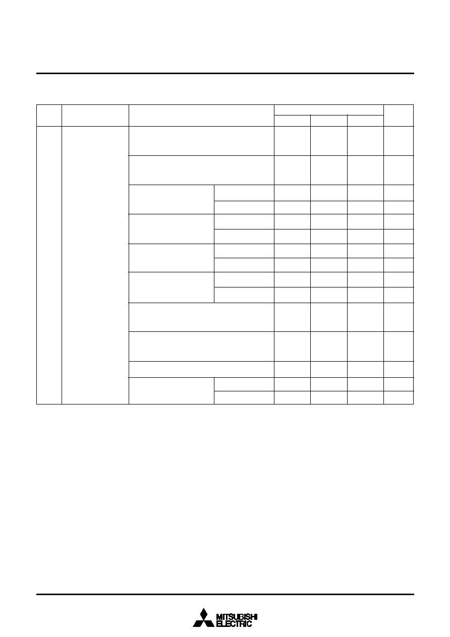
86
SINGLE-CHIP 8-BIT CMOS MICROCOMPUTER
MITSUBISHI MICROCOMPUTERS
Table 29 Electrical characteristics (3) (spec. H)
(V
CC
= 2.7 to 5.5 V, V
SS
= 0 V, T
a
= ≠20 to 85 ∞C, unless otherwise noted)
Power source current
Limits
Parameter
Min.
Typ.
Max.
Symbol
Unit
High-speed mode
f(X
IN
) = 8 MHz
f(X
CIN
) = 32.768 kHz
Output transistors "off"
High-speed mode
f(X
IN
) = 8 MHz (in WIT state)
f(X
CIN
) = 32.768 kHz
Output transistors "off"
Low-speed mode
f(X
IN
) = stopped
f(X
CIN
) = 32.768 kHz
Output transistors "off"
Low-speed mode
f(X
IN
) = stopped
f(X
CIN
) = 32.768 kHz (in WIT state)
Output transistors "off"
Low-speed mode (V
CC
= 3 V)
f(X
IN
) = stopped
f(X
CIN
) = 32.768 kHz
Output transistors "off"
Low-speed mode (V
CC
= 3 V)
f(X
IN
) = stopped
f(X
CIN
) = 32.768 kHz (in WIT state)
Output transistors "off"
Middle-speed mode
f(X
IN
) = 8 MHz
f(X
CIN
) = stopped
Output transistors "off"
Middle-speed mode
f(X
IN
) = 8 MHz (in WIT state)
f(X
CIN
) = stopped
Output transistors "off"
Increment when A-D conversion is executed
f(X
IN
) = 8 MHz
Test conditions
13
I
CC
Ta = 25 ∞C
Ta = 85 ∞C
6.8
mA
All oscillation stopped
(in STP state)
Output transistors "off"
1.6
60
250
20
70
150
5.0
20
4.0
200
mA
µ
A
Except
M38507F8FP/SP
M38507F8FP/SP
Except
M38507F8FP/SP
M38507F8FP/SP
3850 Group (Spec. H)
20
1.5
800
0.1
40
55
10.0
7.0
1.0
10
µ
A
µ
A
µ
A
µ
A
µ
A
µ
A
µ
A
mA
mA
µ
A
µ
A
µ
A
Except
M38507F8FP/SP
M38507F8FP/SP
Except
M38507F8FP/SP
M38507F8FP/SP

87
SINGLE-CHIP 8-BIT CMOS MICROCOMPUTER
MITSUBISHI MICROCOMPUTERS
Table 30 Electrical characteristics (3) (spec. A)
(V
CC
= 2.7 to 5.5 V, V
SS
= 0 V, T
a
= ≠20 to 85 ∞C, unless otherwise noted)
Power source current
Limits
Parameter
Min.
Typ.
Max.
Symbol
Unit
High-speed mode
f(X
IN
) = 12.5 MHz
f(X
CIN
) = 32.768 kHz
Output transistors "off"
High-speed mode
f(X
IN
) = 12.5 MHz (in WIT state)
f(X
CIN
) = 32.768 kHz
Output transistors "off"
Middle-speed mode
f(X
IN
) = 8 MHz
f(X
CIN
) = stopped
Output transistors "off"
Middle-speed mode
f(X
IN
) = 8 MHz (in WIT state)
f(X
CIN
) = stopped
Output transistors "off"
Low-speed mode
f(X
IN
) = stopped
f(X
CIN
) = 32.768 kHz
Output transistors "off"
Low-speed mode
f(X
IN
) = stopped
f(X
CIN
) = 32.768 kHz (in WIT state)
Output transistors "off"
Low-speed mode (Vcc = 3 V)
f(X
IN
) = stopped
f(X
CIN
) = 32.768 kHz
Output transistors "off"
Low-speed mode (Vcc = 3 V)
f(X
IN
) = stopped
f(X
CIN
) = 32.768 kHz (in WIT state)
Output transistors "off"
Increment when A-D conversion is executed
f(X
IN
) = 8 MHz
Test conditions
15
7.0
4.0
200
70
55
10.0
1.0
10
I
CC
Ta = 25 ∞C
Ta = 85 ∞C
7.5
1.6
4.0
1.5
60
40
20
5.0
800
0.1
mA
mA
mA
mA
µ
A
µ
A
µ
A
µ
A
µ
A
µ
A
µ
A
All oscillation stopped
(in STP state)
Output transistors "off"
3850 Group (Spec. A)
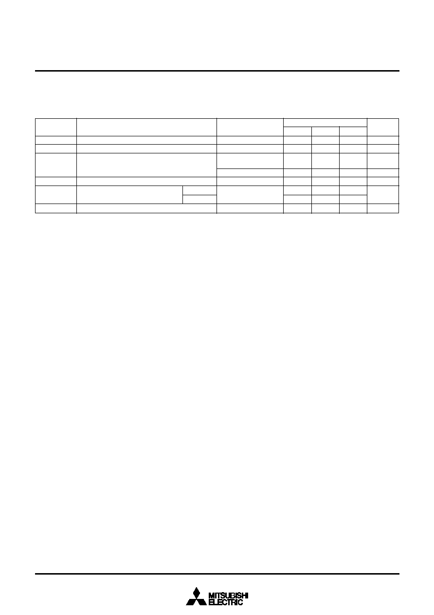
88
SINGLE-CHIP 8-BIT CMOS MICROCOMPUTER
MITSUBISHI MICROCOMPUTERS
A-D converter characteristics
Table 31 A-D converter characteristics (spec. H)
(V
CC
= 2.7 to 5.5 V, V
SS
= AV
SS
= 0 V, T
a
= ≠20 to 85 ∞C, f(X
IN
) = 8 MHz, unless otherwise noted)
bit
LSB
2tc(X
IN
)
µ
s
k
µ
A
µ
A
Resolution
Absolute accuracy (excluding quantization error)
Conversion time
Ladder resistor
Reference power source input current
A-D port input current
Min.
50
Typ.
40
35
150
0.5
Max.
10
±4
61
200
5.0
5.0
High-speed mode,
Middle-speed mode
Low-speed mode
V
REF
= 5.0 V
Unit
Limits
Parameter
≠
≠
t
CONV
R
LADDER
I
VREF
I
I(AD)
Test conditions
Symbol
V
REF
"on"
V
REF
"off"
3850 Group (Spec. H)

89
SINGLE-CHIP 8-BIT CMOS MICROCOMPUTER
MITSUBISHI MICROCOMPUTERS
A-D converter characteristics
Table 32 A-D converter characteristics (spec. A)
(V
CC
= 2.7 to 5.5 V, V
SS
= AV
SS
= 0 V, T
a
= ≠20 to 85 ∞C, f(X
IN
) = 12.5 MHz, unless otherwise noted)
bit
LSB
2tc(X
IN
)
µ
s
k
µ
A
µ
A
Resolution
Absolute accuracy (excluding quantization error)
Conversion time
Ladder resistor
Reference power source input current
A-D port input current
Min.
50
Typ.
40
35
150
0.5
Max.
10
±4
61
200
5.0
5.0
High-speed mode,
Middle-speed mode
Low-speed mode
V
REF
= 5.0 V
Unit
Limits
Parameter
≠
≠
t
CONV
R
LADDER
I
VREF
I
I(AD)
Test conditions
Symbol
V
REF
"on"
V
REF
"off"
3850 Group (Spec. A)

90
SINGLE-CHIP 8-BIT CMOS MICROCOMPUTER
MITSUBISHI MICROCOMPUTERS
Timing requirements
Table 33 Timing requirements (1) (spec. H)
(V
CC
= 4.0 to 5.5 V, V
SS
= 0 V, T
a
= ≠20 to 85 ∞C, unless otherwise noted)
Reset input "L" pulse width
External clock input cycle time
External clock input "H" pulse width
External clock input "L" pulse width
CNTR
0
, CNTR
1
input cycle time
CNTR
0
, CNTR
1
input "H" pulse width
CNTR
0
, CNTR
1
input "L" pulse width
INT
0
to INT
3
input "H" pulse width
INT
0
to INT
3
input "L" pulse width
Serial I/O1 clock input cycle time (Note)
Limits
X
IN
cycle
ns
ns
ns
ns
ns
ns
ns
ns
ns
ns
ns
ns
ns
ns
ns
ns
ns
ns
Parameter
Min.
20
125
50
50
200
80
80
80
80
800
370
370
220
100
1000
400
400
200
200
Typ.
Max.
Symbol
Unit
Note : When f(X
IN
) = 8 MHz and bit 6 of address 001A
16
is "1" (clock synchronous).
Divide this value by four when f(X
IN
) = 8 MHz and bit 6 of address 001A
16
is "0" (UART).
Serial I/O1 clock
input "H" pulse width (Note)
Serial I/O1 clock
input "L" pulse width (Note)
Serial I/O1 input setup time
Serial I/O1 input hold time
Serial I/O2 clock input cycle time
Serial I/O2 clock
input "H" pulse width
Serial I/O2 clock
input "L" pulse width
Serial I/O2 clock input setup time
Serial I/O2 clock input hold time
Table 34 Timing requirements (2) (spec. H)
(V
CC
= 2.7 to 5.5 V, V
SS
= 0 V, T
a
= ≠20 to 85 ∞C, unless otherwise noted)
t
W
(RESET)
t
C
(X
IN
)
t
WH
(X
IN
)
t
WL
(X
IN
)
t
C
(CNTR)
t
WH
(CNTR)
t
WL
(CNTR)
t
WH
(INT)
t
WL
(INT)
t
C
(S
CLK1
)
t
WH
(S
CLK1
)
t
WL
(S
CLK1
)
t
su
(R
x
D-S
CLK1
)
t
h
(S
CLK1
-R
x
D)
t
C
(S
CLK2
)
t
WH
(S
CLK2
)
t
WL
(S
CLK2
)
t
su
(S
IN2
-S
CLK2
)
t
h
(S
CLK2
-S
IN2
)
Reset input "L" pulse width
External clock input cycle time
External clock input "H" pulse width
External clock input "L" pulse width
CNTR
0
, CNTR
1
input cycle time
CNTR
0
, CNTR
1
input "H" pulse width
CNTR
0
, CNTR
1
input "L" pulse width
INT
0
to INT
3
input "H" pulse width
INT
0
to INT
3
input "L" pulse width
Serial I/O1 clock input cycle time (Note)
Serial I/O1 clock
input "H" pulse width (Note)
Serial I/O1 clock
input "L" pulse width (Note)
Serial I/O1 input setup time
Serial I/O1 input hold time
Serial I/O2 clock input cycle time
Serial I/O2 clock
input "H" pulse width
Serial I/O2 clock
input "L" pulse width
Serial I/O2 clock input setup time
Serial I/O2 clock input hold time
t
W
(RESET)
t
C
(X
IN
)
t
WH
(X
IN
)
t
WL
(X
IN
)
t
C
(CNTR)
t
WH
(CNTR)
t
WL
(CNTR)
t
WH
(INT)
t
WL
(INT)
t
C
(S
CLK1
)
t
WH
(S
CLK1
)
t
WL
(S
CLK1
)
t
su
(R
x
D-S
CLK1
)
t
h
(S
CLK1
-R
x
D)
t
C
(S
CLK2
)
t
WH
(S
CLK2
)
t
WL
(S
CLK2
)
t
su
(S
IN2
-S
CLK2
)
t
h
(S
CLK2
-S
IN2
)
Limits
X
IN
cycle
ns
ns
ns
ns
ns
ns
ns
ns
ns
ns
ns
ns
ns
ns
ns
ns
ns
ns
Parameter
Min.
20
250
100
100
500
230
230
230
230
2000
950
950
400
200
2000
950
950
400
300
Typ.
Max.
Symbol
Unit
Note : When f(X
IN
) = 4 MHz and bit 6 of address 001A
16
is "1" (clock synchronous).
Divide this value by four when f(X
IN
) = 4 MHz and bit 6 of address 001A
16
is "0" (UART).
3850 Group (Spec. H)

91
SINGLE-CHIP 8-BIT CMOS MICROCOMPUTER
MITSUBISHI MICROCOMPUTERS
Timing requirements
Table 35 Timing requirements (1) (spec. A)
(V
CC
= 4.0 to 5.5 V, V
SS
= 0 V, T
a
= ≠20 to 85 ∞C, unless otherwise noted)
Reset input "L" pulse width
External clock input cycle time
External clock input "H" pulse width
External clock input "L" pulse width
CNTR
0
, CNTR
1
input cycle time
CNTR
0
, CNTR
1
input "H" pulse width
CNTR
0
, CNTR
1
input "L" pulse width
INT
0
to INT
3
input "H" pulse width
INT
0
to INT
3
input "L" pulse width
Serial I/O1 clock input cycle time (Note)
Limits
X
IN
cycle
ns
ns
ns
ns
ns
ns
ns
ns
ns
ns
ns
ns
ns
ns
ns
ns
ns
ns
Parameter
Min.
20
80
32
32
200
80
80
80
80
800
370
370
220
100
1000
400
400
200
200
Typ.
Max.
Symbol
Unit
Note : When f(X
IN
) = 8 MHz and bit 6 of address 001A
16
is "1" (clock synchronous).
Divide this value by four when f(X
IN
) = 8 MHz and bit 6 of address 001A
16
is "0" (UART).
Serial I/O1 clock
input "H" pulse width (Note)
Serial I/O1 clock
input "L" pulse width (Note)
Serial I/O1 input setup time
Serial I/O1 input hold time
Serial I/O2 clock input cycle time
Serial I/O2 clock
input "H" pulse width
Serial I/O2 clock
input "L" pulse width
Serial I/O2 clock input setup time
Serial I/O2 clock input hold time
Table 36 Timing requirements (2) (spec. A)
(V
CC
= 2.7 to 5.5 V, V
SS
= 0 V, T
a
= ≠20 to 85 ∞C, unless otherwise noted)
t
W
(RESET)
t
C
(X
IN
)
t
WH
(X
IN
)
t
WL
(X
IN
)
t
C
(CNTR)
t
WH
(CNTR)
t
WL
(CNTR)
t
WH
(INT)
t
WL
(INT)
t
C
(S
CLK1
)
t
WH
(S
CLK1
)
t
WL
(S
CLK1
)
t
su
(R
x
D-S
CLK1
)
t
h
(S
CLK1
-R
x
D)
t
C
(S
CLK2
)
t
WH
(S
CLK2
)
t
WL
(S
CLK2
)
t
su
(S
IN2
-S
CLK2
)
t
h
(S
CLK2
-S
IN2
)
Reset input "L" pulse width
External clock input cycle time
External clock input "H" pulse width
External clock input "L" pulse width
CNTR
0
, CNTR
1
input cycle time
CNTR
0
, CNTR
1
input "H" pulse width
CNTR
0
, CNTR
1
input "L" pulse width
INT
0
to INT
3
input "H" pulse width
INT
0
to INT
3
input "L" pulse width
Serial I/O1 clock input cycle time (Note)
Serial I/O1 clock
input "H" pulse width (Note)
Serial I/O1 clock
input "L" pulse width (Note)
Serial I/O1 input setup time
Serial I/O1 input hold time
Serial I/O2 clock input cycle time
Serial I/O2 clock
input "H" pulse width
Serial I/O2 clock
input "L" pulse width
Serial I/O2 clock input setup time
Serial I/O2 clock input hold time
t
W
(RESET)
t
C
(X
IN
)
t
WH
(X
IN
)
t
WL
(X
IN
)
t
C
(CNTR)
t
WH
(CNTR)
t
WL
(CNTR)
t
WH
(INT)
t
WL
(INT)
t
C
(S
CLK1
)
t
WH
(S
CLK1
)
t
WL
(S
CLK1
)
t
su
(R
x
D-S
CLK1
)
t
h
(S
CLK1
-R
x
D)
t
C
(S
CLK2
)
t
WH
(S
CLK2
)
t
WL
(S
CLK2
)
t
su
(S
IN2
-S
CLK2
)
t
h
(S
CLK2
-S
IN2
)
Limits
X
IN
cycle
ns
ns
ns
ns
ns
ns
ns
ns
ns
ns
ns
ns
ns
ns
ns
ns
ns
ns
Parameter
Min.
20
166
66
66
500
230
230
230
230
2000
950
950
400
200
2000
950
950
400
300
Typ.
Max.
Symbol
Unit
Note : When f(X
IN
) = 4 MHz and bit 6 of address 001A
16
is "1" (clock synchronous).
Divide this value by four when f(X
IN
) = 4 MHz and bit 6 of address 001A
16
is "0" (UART).
3850 Group (Spec. A)
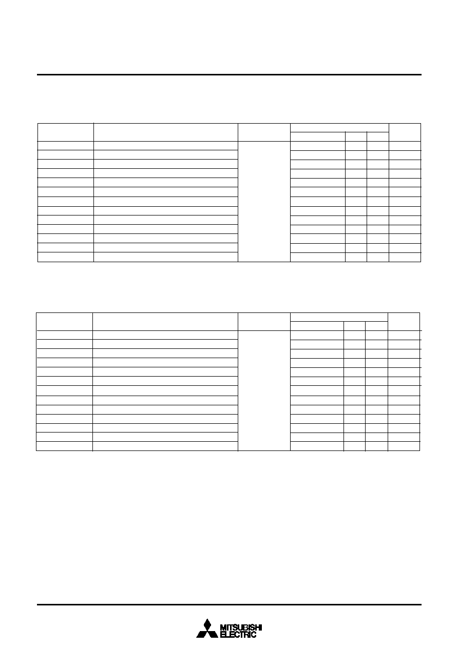
92
SINGLE-CHIP 8-BIT CMOS MICROCOMPUTER
MITSUBISHI MICROCOMPUTERS
Table 37 Switching characteristics (1)
(V
CC
= 4.0 to 5.5 V, V
SS
= 0 V, T
a
= ≠20 to 85 ∞C, unless otherwise noted)
Table 38 Switching characteristics (2)
(V
CC
= 2.7 to 5.5 V, V
SS
= 0 V, T
a
= ≠20 to 85 ∞C, unless otherwise noted)
Serial I/O1 clock output "H" pulse width
Serial I/O1 clock output "L" pulse width
Serial I/O1 output delay time (Note 1)
Serial I/O1 output valid time (Note 1)
Serial I/O1 clock output rising time
Serial I/O1 clock output falling time
Serial I/O2 clock output "H" pulse width
Serial I/O2 clock output "L" pulse width
Serial I/O2 output delay time (Note 2)
Serial I/O2 output valid time (Note 2)
Serial I/O2 clock output falling time
CMOS output rising time (Note 3)
CMOS output falling time (Note 3)
t
WH
(S
CLK1
)
t
WL
(S
CLK1
)
t
d
(S
CLK1
-T
X
D)
t
v
(S
CLK1
-T
X
D)
t
r
(S
CLK1
)
t
f
(S
CLK1
)
t
WH
(S
CLK2
)
t
WL
(S
CLK2
)
t
d
(S
CLK2
-S
OUT2
)
t
v
(S
CLK2
-S
OUT2
)
t
f
(S
CLK2
)
t
r
(CMOS)
t
f
(CMOS)
Limits
ns
ns
ns
ns
ns
ns
ns
ns
ns
ns
ns
ns
ns
Parameter
Min.
t
C
(S
CLK1
)/2≠30
t
C
(S
CLK1
)/2≠30
≠30
t
C
(S
CLK2
)/2≠160
t
C
(S
CLK2
)/2≠160
0
Typ.
10
10
Max.
140
30
30
200
30
30
30
Symbol
Unit
Notes 1: When the P2
5
/T
X
D P-channel output disable bit of the UART control register (bit 4 of address 001B
16
) is "0".
2: When the P0
1
/S
OUT2
and P0
2
/S
CLK2
P-channel output disable bit of the Serial I/O2 control register 1 (bit 7 of address 0015
16
) is "0".
3: The X
OUT
pin is excluded.
Test conditions
Fig. 78
Serial I/O1 clock output "H" pulse width
Serial I/O1 clock output "L" pulse width
Serial I/O1 output delay time (Note 1)
Serial I/O1 output valid time (Note 1)
Serial I/O1 clock output rising time
Serial I/O1 clock output falling time
Serial I/O2 clock output "H" pulse width
Serial I/O2 clock output "L" pulse width
Serial I/O2 output delay time (Note 2)
Serial I/O2 output valid time (Note 2)
Serial I/O2 clock output falling time
CMOS output rising time (Note 3)
CMOS output falling time (Note 3)
t
WH
(S
CLK1
)
t
WL
(S
CLK1
)
t
d
(S
CLK1
-T
X
D)
t
v
(S
CLK1
-T
X
D)
t
r
(S
CLK1
)
t
f
(S
CLK1
)
t
WH
(S
CLK2
)
t
WL
(S
CLK2
)
t
d
(S
CLK2
-S
OUT2
)
t
v
(S
CLK2
-S
OUT2
)
t
f
(S
CLK2
)
t
r
(CMOS)
t
f
(CMOS)
Limits
ns
ns
ns
ns
ns
ns
ns
ns
ns
ns
ns
ns
ns
Parameter
Min.
t
C
(S
CLK1
)/2≠50
t
C
(S
CLK1
)/2≠50
≠30
t
C
(S
CLK2
)/2≠240
t
C
(S
CLK2
)/2≠240
0
Typ.
20
20
Max.
350
50
50
400
50
50
50
Symbol
Unit
Notes 1: When the P2
5
/T
X
D P-channel output disable bit of the UART control register (bit 4 of address 001B
16
) is "0".
2: When the P0
1
/S
OUT2
and P0
2
/S
CLK2
P-channel output disable bit of the Serial I/O2 control register 1 (bit 7 of address 0015
16
) is "0".
3: The X
OUT
pin is excluded.
Test conditions
Fig. 78
3850 Group (Spec. H/A)
Switching characteristics

93
SINGLE-CHIP 8-BIT CMOS MICROCOMPUTER
MITSUBISHI MICROCOMPUTERS
Fig. 78 Circuit for measuring output switching characteristics
3850 Group (Spec. H/A)
Measurement output pin
100 pF
C
M
O
S
o
u
t
p
u
t
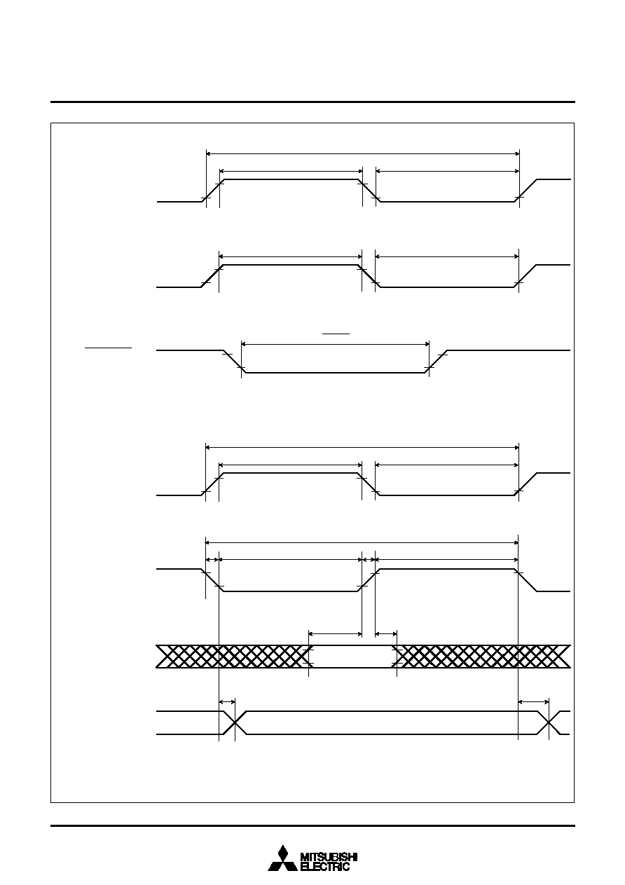
94
SINGLE-CHIP 8-BIT CMOS MICROCOMPUTER
MITSUBISHI MICROCOMPUTERS
Fig. 79 Timing diagram
3850 Group (Spec. H/A)
t
C
(
C
N
T
R
)
0
.
2
V
C
C
t
W
L
(
I
N
T
)
0
.
8
V
C
C
t
W
H
(
I
N
T
)
0
.
2
V
C
C
0
.
8
V
C
C
t
W
(
R
E
S
E
T
)
R
E
S
E
T
0
.
2
V
C
C
t
W
L
(
C
N
T
R
)
0
.
8
V
C
C
t
W
H
(
C
N
T
R
)
0
.
2
V
C
C
0
.
2
V
C
C
0
.
8
V
C
C
0.8V
CC
0.2V
CC
t
WL(X
IN
)
0
.
8
V
C
C
t
WH(X
IN
)
t
C
(
X
I
N
)
X
I
N
t
f
t
r
t
d
(
S
C
L
K
1
-
T
X
D
)
,
t
d
(
S
C
L
K
2
-
S
O
U
T
2
)
t
v
(
S
C
L
K
1
-
T
X
D
)
,
t
v
(
S
C
L
K
2
-
S
O
U
T
2
)
t
C
(
S
C
L
K
1
)
,
t
C
(
S
C
L
K
2
)
t
W
L
(
S
C
L
K
1
)
,
t
W
L
(
S
C
L
K
2
)
t
W
H
(
S
C
L
K
1
)
,
t
W
H
(
S
C
L
K
2
)
t
h
(
S
C
L
K
1
-
R
x
D
)
,
t
h
(
S
C
L
K
2
-
S
I
N
2
)
t
s
u
(
R
x
D
-
S
C
L
K
1
)
,
t
s
u
(
S
I
N
2
-
S
C
L
K
2
)
T
X
D
S
OUT2
R
X
D
S
I
N
2
S
C
L
K
1
S
C
L
K
2
I
N
T
0
t
o
I
N
T
3
CNTR
0
CNTR
1

95
SINGLE-CHIP 8-BIT CMOS MICROCOMPUTER
MITSUBISHI MICROCOMPUTERS
3850 Group (Spec. H/A)
PACKAGE OUTLINE
SDIP42-P-600-1.78
Weight(g)
≠
JEDEC Code
4.1
EIAJ Package Code
Lead Material
Alloy 42/Cu Alloy
42P4B
Plastic 42pin 600mil SDIP
Symbol
Min
Nom
Max
A
A
2
b
b
1
b
2
c
E
D
L
Dimension in Millimeters
A
1
0.51
≠
≠
≠
3.8
≠
0.35
0.45
0.55
0.9
1.0
1.3
0.63
0.73
1.03
0.22
0.27
0.34
36.5
36.7
36.9
12.85
13.0
13.15
≠
1.778
≠
≠
15.24
≠
3.0
≠
≠
0
∞
≠
15
∞
≠
≠
5.5
e
e
1
42
22
21
1
E
c
e
1
A
2
A
1
b
b
1
b
2
e
L
A
SEATING PLANE
D
MMP
SSOP42-P-450-0.80
Weight(g)
≠
JEDEC Code
0.63
EIAJ Package Code
Lead Material
Alloy 42
42P2R-A/E
Plastic 42pin 450mil SSOP
Symbol
Min
Nom
Max
A
A
2
b
c
D
E
L
L
1
y
Dimension in Millimeters
H
E
A
1
I
2
≠
≠
.25
0
.05
0
.13
0
.3
17
.2
8
≠
.63
11
.3
0
≠
≠
≠
.27
1
≠
≠
.0
2
.3
0
.15
0
.5
17
.4
8
.8
0
.93
11
.5
0
.765
1
≠
.43
11
≠
≠
.4
2
≠
.4
0
.2
0
.7
17
.6
8
≠
.23
12
.7
0
≠
.15
0
≠
b
2
≠
.5
0
≠
≠
0
∞
≠
10
∞
e
e
1
42
22
21
1
H
E
E
D
e
y
F
A
A
2
A
1
L
1
L
c
e
b
2
e
1
I
2
Recommended Mount Pad
Detail F
z
Z
1
Detail G
≠
≠
Z
1
0.75
≠
≠
0.9
z
b
G
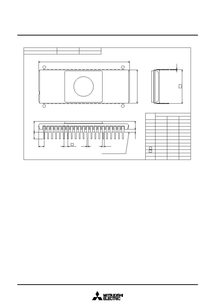
96
SINGLE-CHIP 8-BIT CMOS MICROCOMPUTER
MITSUBISHI MICROCOMPUTERS
3850 Group (Spec. H/A)
WDIP42-C-600-1.78
Weight(g)
JEDEC Code
EIAJ Package Code
42S1B-A
Metal seal 42pin 600mil DIP
≠
≠
≠
≠
≠
≠
0.46
0.25
≠
≠
3.44
15.8
≠
≠
≠
≠
≠
≠
3.05
≠
≠
≠
≠
≠
Symbol
Min
Nom
Max
A
A
2
b
b
1
c
D
E
L
Z
Dimension in Millimeters
A
1
3.05
15.24
1.778
41.1
0.33
0.17
0.9
0.8
0.7
0.54
0.38
1.0
5.0
e
e
1
e
E
D
1
42
22
21
b
Z
SEATING PLANE
A
L
A
2
A
1
b
1
e
1
c

3850 Group (Spec. H/A)
SINGLE-CHIP 8-BIT CMOS MICROCOMPUTER
MITSUBISHI MICROCOMPUTERS
© 2002 MITSUBISHI ELECTRIC CORP.
New publication, effective May 2002.
Specifications subject to change without notice.
Notes regarding these materials
∑
These materials are intended as a reference to assist our customers in the selection of the Mitsubishi semiconductor product best suited to the customer's application; they do not convey any license under any intellectual property
rights, or any other rights, belonging to Mitsubishi Electric Corporation or a third party.
∑
Mitsubishi Electric Corporation assumes no responsibility for any damage, or infringement of any third-party's rights, originating in the use of any product data, diagrams, charts, programs, algorithms, or circuit application examples
contained in these materials.
∑
All information contained in these materials, including product data, diagrams, charts, programs and algorithms represents information on products at the time of publication of these materials, and are subject to change by
Mitsubishi Electric Corporation without notice due to product improvements or other reasons. It is therefore recommended that customers contact Mitsubishi Electric Corporation or an authorized Mitsubishi Semiconductor product
distributor for the latest product information before purchasing a product listed herein.
The information described here may contain technical inaccuracies or typographical errors. Mitsubishi Electric Corporation assumes no responsibility for any damage, liability, or other loss rising from these inaccuracies or errors.
Please also pay attention to information published by Mitsubishi Electric Corporation by various means, including the Mitsubishi Semiconductor home page (http://www.mitsubishichips.com).
∑
When using any or all of the information contained in these materials, including product data, diagrams, charts, programs, and algorithms, please be sure to evaluate all information as a total system before making a final decision
on the applicability of the information and products. Mitsubishi Electric Corporation assumes no responsibility for any damage, liability or other loss resulting from the information contained herein.
∑
Mitsubishi Electric Corporation semiconductors are not designed or manufactured for use in a device or system that is used under circumstances in which human life is potentially at stake. Please contact Mitsubishi Electric
Corporation or an authorized Mitsubishi Semiconductor product distributor when considering the use of a product contained herein for any specific purposes, such as apparatus or systems for transportation, vehicular, medical,
aerospace, nuclear, or undersea repeater use.
∑
The prior written approval of Mitsubishi Electric Corporation is necessary to reprint or reproduce in whole or in part these materials.
∑
If these products or technologies are subject to the Japanese export control restrictions, they must be exported under a license from the Japanese government and cannot be imported into a country other than the approved
destination.
Any diversion or reexport contrary to the export control laws and regulations of Japan and/or the country of destination is prohibited.
∑
Please contact Mitsubishi Electric Corporation or an authorized Mitsubishi Semiconductor product distributor for further details on these materials or the products contained therein.
Keep safety first in your circuit designs!
∑
Mitsubishi Electric Corporation puts the maximum effort into making semiconductor products better and more reliable, but there is always the possibility that trouble may occur with them. Trouble with semiconductors may lead to
personal injury, fire or property damage. Remember to give due consideration to safety when making your circuit designs, with appropriate measures such as (i) placement of substitutive, auxiliary circuits, (ii) use of non-flammable
material or (iii) prevention against any malfunction or mishap.
HEAD OFFICE: 2-2-3, MARUNOUCHI, CHIYODA-KU, TOKYO 100-8310, JAPAN

REVISION HISTORY
3850 GROUP (Spec. H/A) DATA SHEET
Rev.
Date
Description
Page
Summary
(1/2)
1.0
03/09/00
First Edition
1
1
6
17
23
27
33
36
38 to 71
41
72
73
73
73
77
79
79
1.1
03/22/00
Font errors are revised.
2.0
12/22/00
"lInterrupts" of "FEATURES" is revised.
Figure 1 is partly revised.
Table 3 is partly revised.
Explanations of "INTERRUPTS" are partly revised.
Figure 20 is partly revised.
Figure 24 is partly revised.
Explanations of "RESET CIRCUIT" are partly revised.
Note 1 into Figure 42 is partly revised.
Explanations of "FLASH MEMORY VERSION" are added.
Figure 45 is partly revised.
"EPROM Version/One Time PROM Version/Flash Memory Version" of "NOTES
ON USAGE" is added.
"DATA REQUIRED FOR MASK ORDERS" is added.
"DATA REQUIRED FOR One Time PROM PROGRAMMING ORDERS" is added.
"ROM PROGRAMMING METHOD" is added.
Table 32 is partly revised.
Limit of tw(RESET) into Table 34 is revised.
Limit of tw(RESET) into Table 35 is revised.
3.0
05/29/02
1
7
8
9
9
9
9
10
13
15
27
30
35
49
51
51
52
53
53
54
55
56
q
Explanations of "Spec. A" are added.
P2, P4, P6, P16, P18, P22-P26, P42,P43, P47, P82, P84, P87, P89, P91
q
Power dissipation is partly revised.
Figure 5 is partly revised.
Figure 6 is partly revised.
Table 3 3850 group (standard) and 3850 group (spec. H) corresponding prod-
ucts of Rev.2.0 is eliminated.
Table 4 is added.
Table 5 is partly added.
Clause name and explanations of "Notes on differences among 3850 group
(standard), 3850 group (spec. H), and 3850 group (spec. A)" are partly added.
Explanations of "CENTRAL PROCESSING UNIT (CPU)" are partly added.
Figure 9 is partly revised.
Figure 11 is partly revised.
s
Notes is revised.
s
Notes is partly added.
s
Notes on serial I/O is added.
Figure 55 is partly revised.
Explanations of "FLASH MEMORY MODE" is partly revised.
Table 11 is partly revised.
Clause name of "Microcomputer Mode and Boot Mode" is revised.
Explanations of "Outline Performance (CPU Rewrite Mode)" are partly revised.
Figure 58 is partly revised.
Figure 59 is partly revised.
Explanations of "(1) Operation speed" are partly revised.
Explanations of "Software Commands (CPU Rewrite Mode)" are partly revised.

REVISION HISTORY
3850 GROUP (Spec. H/A) DATA SHEET
Rev.
Date
Description
Page
Summary
(2/2)
3.0
05/29/02
56
56
56
57
57
58
59
60
60
62
63
65
77
77
77
78
78
79
86
Explanations of "
q
Read Array Command (FF
16
)" are partly eliminated.
Explanations of "
q
Read Status Register Command (70
16
)" are partly revised.
Explanations of "
q
Program Command (40
16
)" are partly revised.
Explanations of "
q
Erase All Blocks Command (20
16
/20
16
)" are partly revised.
Explanations of "
q
Block Erase Command (20
16
/D0
16
)" are partly revised.
Explanations of "Status Register (SRD)" are partly reveised.
Figure 62 is partly revised.
Explanations of "
q
ROM Code Protect Function (in Parallel I/O Mode)" is partly
revised.
Figure 63 is partly revised.
Contents of "(2) Parallel I/O Mode" are revised.
(Explanations, figures, and tables of Pages 61≠67 in Rev. 2.0 except "Parallel
I/O Mode" and "User ROM and Boot ROM Areas" are eliminated.)
Explanations of "(3) Standard serial I/O Mode" are partly revised.
Figure 65 is partly revised.
Limits of V
I
(CNVss) into Table 18 are revised.
Item of V
IL
, V
IH
into Table 19 are eliminated.
Figures and tables of Pages 79≠84 in Rev. 2.0 are eliminated.
Explanations of "A-D converter" are partly eliminated.
Clause name and explanations of "Differences among 3850 group (standard),
3850 group (spec. H), and 3850 group (spec. A)" are partly revised.
"Electric Characteristic Differences Among Mask ROM, Flash Memory, and
One Time PROM Version MCUs" is added.
Test conditions of Low-speed mode of Icc are partly added.