Document Outline
- DESCRIPTION
- FEATURES
- APPLICATION
- PIN CONFIGURATION
- M38867M8A-XXXHP, M38867E8AHP
- M38867E8AFS
- M38869MFA-XXXGP/HP, M38869FFAGP/HP
- FUNCTIONAL BLOCK
- PIN DESCRIPTION
- PART NUMBERING
- GROUP EXPANSION
- FUNCTIONAL DESCRIPTION
- CENTRAL PROCESSING UNIT (CPU)
- [CPU Mode Register (CPUM)]
- MEMORY
- Special Function Register (SFR) Area
- RAM
- ROM
- Interrupt Vector Area
- Zero Page
- Special Page
- I/O PORTS
- INTERRUPTS
- Interrupt Control
- Interrupt Operation
- Interrupt Source Selection
- External Interrupt Pin Selection
- Notes
- Key Input Interrupt (Key-on Wake Up)
- TIMERS
- Timer 1 and Timer 2
- Timer X and Timer Y
- (1) Timer Mode
- (2) Pulse Output Mode
- (3) Event Counter Mode
- (4) Pulse Width Measurement Mode
- SERIAL I/O
- Serial I/O1
- (1) Clock Synchronous Serial I/O Mode
- (2) Asynchronous Serial I/O (UART) Mode
- [Serial I/O1 Control Register (SIO1CON)]
- [UART Control Register (UARTCON)]
- [Serial I/O1 Status Register (SIO1STS)]
- [Transmit Buffer Register/Receive Buffer Register (TB/RB)]
- [Baud Rate Generator (BRG)]
- Serial I/O2
- [Serial I/O2 Control Register (SIO2CON)]
- PULSE WIDTH MODULATION (PWM) OUTPUT CIRCUIT
- Data Setup (PWM0)
- PWM Operation
- Transfer From Register to Latch
- BUS INTERFACE
- [Data Bus Buffer Status Register 0, 1 (DBBSTS0, DBBSTS1)]
- [Input Data Bus Buffer Register 0, 1 (DBBIN0, DBBIN1)]
- [Output Data Bus Buffer Register 0, 1 (DBBOUT0, DBBOUT1)]
- MULTI-MASTER I2C-BUS INTERFACE
- [I2C Data Shift Register (S0)]
- [I2C Address Register (S0D)]
- [I2C Clock Control Register (S2)]
- [I2C Control Register (S1D)]
- [I2C Status Register (S1)]
- START Condition Generating Method
- STOP Condition Generating Method
- START/STOP Condition Detecting Operation
- [I2C START/STOP Condition Control Register (S2D)]
- Address Data Communication
- Example of Master Transmission
- Example of Slave Reception
- Precautions when using multi-master I2C-BUS interface
- A-D CONVERTER
- [A-D Conversion Register 1, 2 (AD1, AD2)]
- [AD/DA Control Register (ADCON)]
- Comparison Voltage Generator
- Channel Selector
- Comparator and Control Circuit
- D-A CONVERTER
- COMPARATOR CIRCUIT
- Comparator Configuration
- Comparator Operation
- WATCHDOG TIMER
- Standard Operation of Watchdog Timer
- Initial Value of Watchdog Timer
- RESET CIRCUIT
- CLOCK GENERATING CIRCUIT
- Frequency Control
- (1) Middle-speed mode
- (2) High-speed mode
- (3) Low-speed mode
- (4) Low power dissipation mode
- Oscillation Control
- (1) Stop mode
- (2) Wait mode
- PROCESSOR MODE
- (1) Single-chip mode
- (2) Memory expansion mode
- (3) Microprocessor mode
- BUS CONTROL AT MEMORY EXPANSION
- EPROM MODE
- FLASH MEMORY MODE
- (1) Flash memory mode 1 (parallel I/O mode)
- Functional Outline (parallel input/output mode)
- Read-only Mode
- Read/Write Mode
- (2) Flash memory mode 2 (serial I/O mode)
- Functional Outline (serial I/O mode)
- (3) Flash memory mode 3 (CPU reprogramming mode)
- Functional Outline (CPU reprogramming mode)
- NOTES ON PROGRAMMING
- Processor Status Register
- Interrupts
- Decimal Calculations
- Timers
- Multiplication and Division Instructions
- Ports
- Serial I/O
- A-D Converter
- D-A Converter
- Instruction Execution Time
- NOTES ON USAGE
- Handling of Power Source Pins
- EPROM version/One Time PROM version/Flash memory version
- Erasing of Flash memory version
- DATA REQUIRED FOR MASK ORDERS
- DATA REQUIRED FOR One Time PROM PROGRAMMING ORDERS
- ELECTRICAL CHARACTERISTICS
- Absolute maximum ratings
- Recommended operating conditions (1)
- Recommended operating conditions (2)
- Recommended operating conditions (3)
- Electrical characteristics (1)
- Electrical characteristics (2)
- A-D converter characteristics (1)
- A-D converter characteristics (2)
- D-A converter characteristics
- Comparator characteristics
- TIMING REQUIREMENTS
- Timing requirements (1)
- Timing requirements (2)
- Timing requirements for system bus interface (1)
- Timing requirements for system bus interface (2)
- Switching characteristics (1)
- Switching characteristics (2)
- Switching characteristics for system bus interface (1)
- Switching characteristics for system bus interface (2)
- Timing requirements in memory expansion mode and microprocessor mode
- Switching characteristics in memory expansion mode and microprocessor mode
- Timing diagram (1) (in single-chip mode)
- Timing diagram (2) (in memory expansion mode and microprocessor mode)
- Timing diagram (3) (in memory expansion mode and microprocessor mode)
- Timing diagram (4) (system bus interface)
- Multi-master I2C-BUS bus line characteristics
- Timing diagram of multi-master I2C-BUS
- PACKAGE OUTLINE
- REVISION DESCRIPTION LIST

DESCRIPTION
The 3886 group is the 8-bit microcomputer based on the 740 fam-
ily core technology.
The 3886 group is designed for controlling systems that require
analog signal processing and include two serial I/O functions, A-D
converters, D-A converters, system data bus interface function,
watchdog timer, and comparator circuit.
The multi-master I
2
C bus interface can be added by option.
FEATURES
<Microcomputer mode>
q
Basic machine-language instructions ...................................... 71
q
Minimum instruction execution time .................................. 0.4
µ
s
(at 10 MHz oscillation frequency)
q
Memory size
ROM ................................................................. 32K to 60K bytes
RAM ............................................................... 1024 to 2048 bytes
q
Programmable input/output ports ............................................ 72
q
Software pull-up resistors ................................................. Built-in
q
Interrupts ................................................. 21 sources, 16 vectors
(Included key input interrupt)
q
Timers ............................................................................. 8-bit
!
4
q
Serial I/O1 .................... 8-bit
!
1(UART or Clock-synchronized)
q
Serial I/O2 ................................... 8-bit
!
1(Clock-synchronized)
q
PWM output circuit ....................................................... 14-bit
!
2
q
Bus interface .................................................................... 2 bytes
q
I
2
C bus interface (option) ............................................. 1 channel
q
A-D converter ............................................... 10-bit
!
8 channels
q
D-A converter ................................................. 8-bit
!
2 channels
q
Comparator circuit ...................................................... 8 channels
q
Watchdog timer ............................................................ 16-bit
!
1
q
Clock generating circuit ..................................... Built-in 2 circuits
(connect to external ceramic resonator or quartz-crystal oscillator)
q
Power source voltage
In high-speed mode .................................................. 4.0 to 5.5 V
(at 10 MHz oscillation frequency)
In middle-speed mode ........................................... 2.7 to 5.5 V(*)
(at 10 MHz oscillation frequency)
In low-speed mode ............................................... 2.7 to 5.5 V (*)
(at 32 kHz oscillation frequency)
(*: 4.0 to 5.5 V for Flash memory version)
3886 Group
SINGLE-CHIP 8-BIT CMOS MICROCOMPUTER
MITSUBISHI MICROCOMPUTERS
q
Power dissipation
In high-speed mode .......................................................... 40 mW
(at 10 MHz oscillation frequency, at 5 V power source voltage)
In low-speed mode ............................................................ 60
µ
W
(at 32 kHz oscillation frequency, at 3 V power source voltage)
q
Memory expansion possible (only for M38867M8A/E8A)
q
Operating temperature range .................................... ≠20 to 85∞C
<Flash memory mode>
q
Supply voltage ................................................. V
CC
= 5 V ± 10 %
q
Program/Erase voltage ............................... V
PP
= 11.7 to 12.6 V
q
Programming method ...................... Programming in unit of byte
q
Erasing method
Batch erasing ........................................ Parallel/Serial I/O mode
Block erasing .................................... CPU reprogramming mode
q
Program/Erase control by software command
q
Number of times for programming/erasing ............................ 100
q
Operating temperature range (at programming/erasing)
..................................................................... Normal temperature
s
Notes
1. The flash memory version cannot be used for application em-
bedded in the MCU card.
2. Power source voltage Vcc of the flash memory version is 4.0
to 5.5 V.
APPLICATION
Household product, consumer electronics, communications, note
book PC, etc.
2
3886 Group
SINGLE-CHIP 8-BIT CMOS MICROCOMPUTER
MITSUBISHI MICROCOMPUTERS
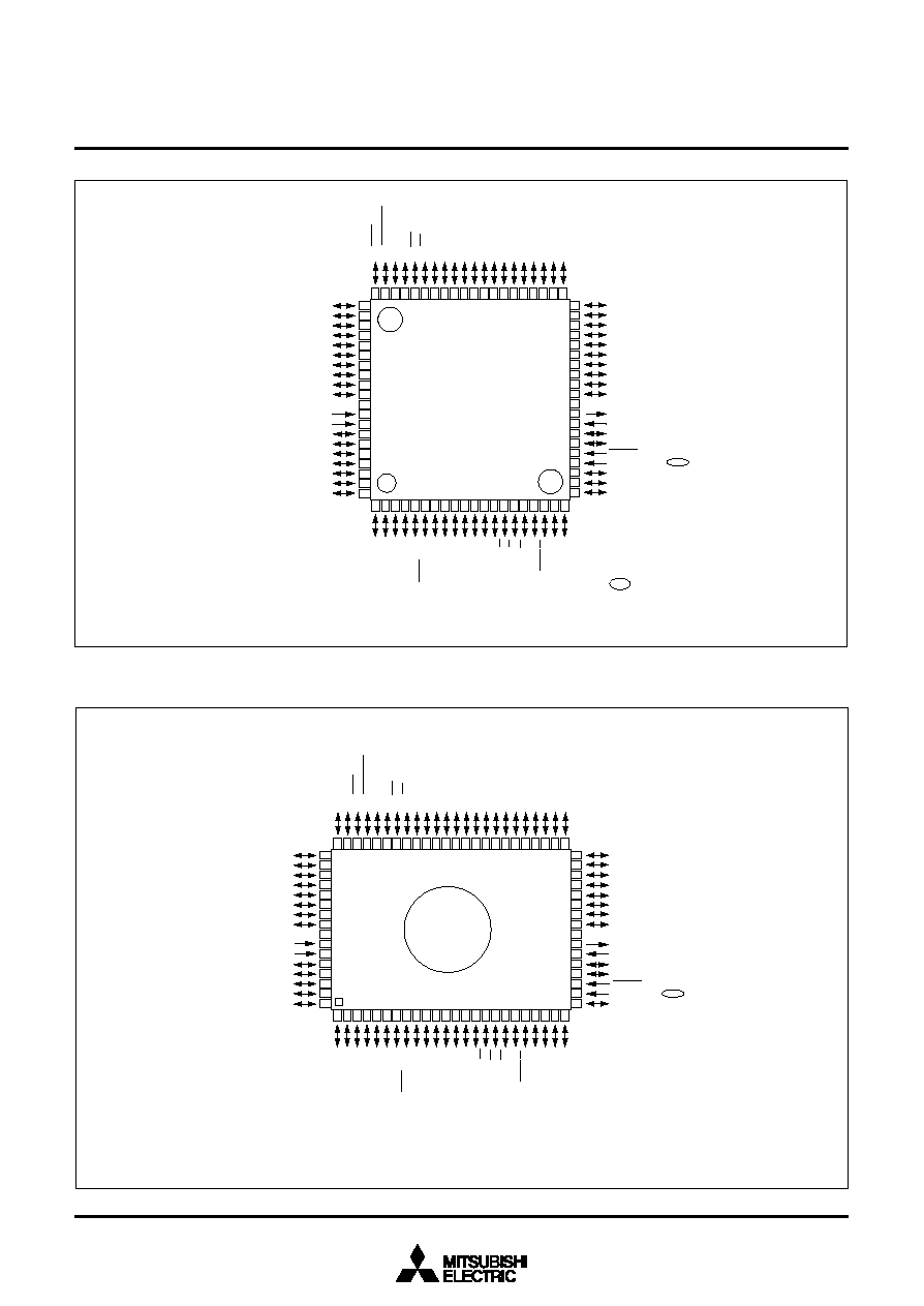
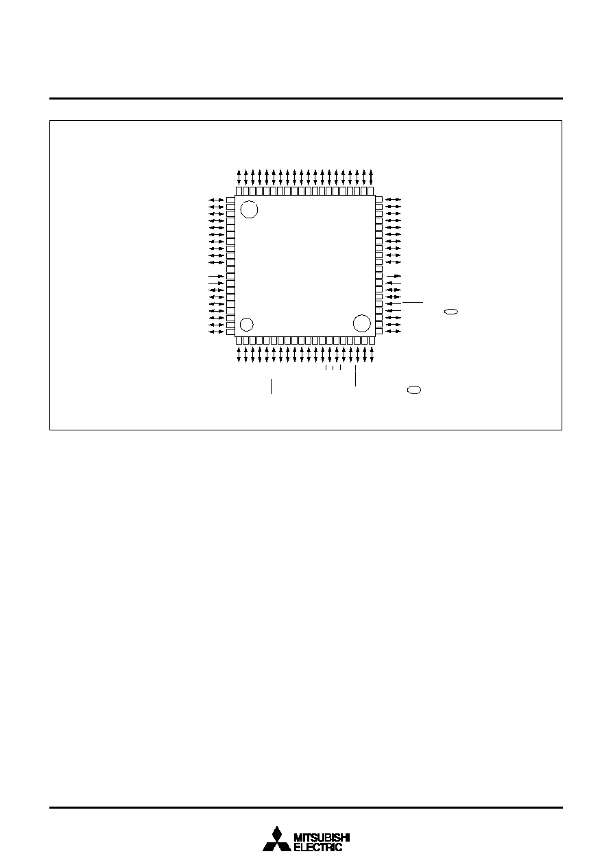
Package type : 80D0
PIN CONFIGURATION (TOP VIEW)
Note: The pin number and the position of
the function pin may change by the
kind of package.
Fig. 2 M38867E8AFS pin configuration
Package type : 80P6Q-A
PIN CONFIGURATION (TOP VIEW)
Note: The pin number and the position of the
function pin may change by the kind of
package.
Fig. 1 M38867M8A-XXXHP, M38867E8AHP pin configuration
: PROM version
2
1
2
2
2
3
2
4
2
5
2
6
2
7
2
8
2
9
3
0
3
1
3
2
3
3
3
4
3
5
3
6
3
7
3
8
3
9
4
0
4
1
4
2
4
3
4
4
4
5
4
6
4
7
4
8
4
9
5
0
5
1
5
2
5
3
5
4
5
5
5
6
5
7
5
8
5
9
6
0
6
1
6
2
6
3
6
4
6
5
6
6
6
7
6
8
6
9
7
0
7
1
7
2
7
3
7
4
7
5
7
6
7
7
7
8
7
9
8
0
P
3
0
/
P
W
M
0
0
P
3
1
/
P
W
M
1
0
P
6
2
/
A
N
2
P
6
1
/
A
N
1
P
4
4
/
R
X
D
P
4
3
/
I
N
T
1
/
O
B
F
0
1
P
6
3
/
A
N
3
P
6
4
/
A
N
4
P
6
5
/
A
N
5
P
6
6
/
A
N
6
A
V
S
S
P
6
7
/
A
N
7
V
R
E
F
V
C
C
P
8
0
/
D
Q
0
P
8
1
/
D
Q
1
P
8
2
/
D
Q
2
P
8
3
/
D
Q
3
P
8
4
/
D
Q
4
P
8
5
/
D
Q
5
P
8
6
/
D
Q
6
P
8
7
/
D
Q
7
P
4
2
/
I
N
T
0
/
O
B
F
0
0
C
N
V
S
S
X
I
N
X
O
U
T
V
S
S
R
E
S
E
T
P
4
0
/
X
C
O
U
T
P
4
1
/
X
C
I
N
P
1
6
/
A
D
1
4
P
1
7
/
A
D
1
5
P
2
6
/
D
B
6
P
2
5
/
D
B
5
P
2
4
/
D
B
4
P
2
3
/
D
B
3
P
2
2
/
D
B
2
P
2
1
/
D
B
1
P
2
0
/
D
B
0
P
3
4
/
P
3
5
/
S
Y
N
C
P
0
0
/
P
3
R
E
F
/
A
D
0
P
0
4
/
A
D
4
P
0
5
/
A
D
5
P
0
6
/
A
D
6
P
0
7
/
A
D
7
P
1
1
/
A
D
9
P
1
2
/
A
D
1
0
P
1
3
/
A
D
1
1
P
1
4
/
A
D
1
2
P
1
5
/
A
D
1
3
P
1
0
/
A
D
8
P
0
1
/
A
D
1
P
0
2
/
A
D
2
P
3
2
/
O
N
W
P
3
3
/
R
E
S
E
T
O
U
T
P
3
6
/
W
R
P
3
7
/
R
D
P
0
3
/
A
D
3
P
2
7
/
D
B
7
P
6
0
/
A
N
0
P
7
7
/
S
C
L
P
7
6
/
S
D
A
P
7
5
/
I
N
T
4
1
P
7
4
/
I
N
T
3
1
P
7
2
/
S
C
L
K
2
P
7
1
/
S
O
U
T
2
P
7
0
/
S
I
N
2
P
5
7
/
D
A
2
/
P
W
M
1
1
P
5
0
/
A
0
P
4
5
/
T
X
D
P
7
3
/
S
R
D
Y
2
/
I
N
T
2
1
P
5
5
/
C
N
T
R
1
P
5
4
/
C
N
T
R
0
P
5
6
/
D
A
1
/
P
W
M
0
1
P
4
7
/
S
R
D
Y
1
/
S
1
P
5
2
/
I
N
T
3
0
/
R
P
5
3
/
I
N
T
4
0
/
W
P
5
1
/
I
N
T
2
0
/
S
0
P
4
6
/
S
C
L
K
1
/
O
B
F
1
0
1
2
3
4
7
8
9
1
0
1
1
1
2
1
3
1
4
1
5
1
6
1
7
1
8
1
9
2
0
5
6
M
3
8
8
6
7
M
8
A
-
X
X
X
H
P
M
3
8
8
6
7
E
8
A
H
P
V
P
P
1
2
5
2
6
2
7
2
8
2
9
3
0
3
1
3
2
3
3
3
4
3
5
3
6
3
7
3
8
3
9
4
0
6
5
6
6
6
7
6
8
6
9
7
0
7
1
7
2
7
3
7
4
7
5
7
6
7
7
7
8
7
9
8
0
2
3
4
5
6
7
8
9
1
0
1
1
1
2
1
3
1
4
1
5
1
6
1
7
1
8
1
9
2
0
2
1
2
2
2
3
2
4
6
4
6
3
6
2
6
1
6
0
5
9
5
8
5
7
5
6
5
5
5
4
5
3
5
2
5
1
5
0
4
9
4
8
4
7
4
6
4
5
4
4
4
3
4
2
4
1
P
3
0
/
P
W
M
0
0
P
3
1
/
P
W
M
1
0
P
3
4
/
P
3
5
/
S
Y
N
C
P
0
0
/
P
3
R
E
F
/
A
D
0
P
0
3
/
A
D
3
P
0
4
/
A
D
4
P
0
5
/
A
D
5
P
0
6
/
A
D
6
P
0
7
/
A
D
7
P
1
1
/
A
D
9
P
1
2
/
A
D
1
0
P
1
3
/
A
D
1
1
P
1
4
/
A
D
1
2
P
1
5
/
A
D
1
3
P
1
6
/
A
D
1
4
P
1
7
/
A
D
1
5
P
6
2
/
A
N
2
P
6
1
/
A
N
1
P
6
0
/
A
N
0
P
7
7
/
S
C
L
P
7
6
/
S
D
A
P
7
5
/
I
N
T
4
1
P
7
4
/
I
N
T
3
1
P
7
2
/
S
C
L
K
2
P
7
1
/
S
O
U
T
2
P
7
0
/
S
I
N
2
P
5
7
/
D
A
2
/
P
W
M
1
1
P
5
0
/
A
0
P
4
6
/
S
C
L
K
1
/
O
B
F
1
0
P
4
5
/
T
X
D
P
4
4
/
R
X
D
P
4
3
/
I
N
T
1
/
O
B
F
0
1
P
6
6
/
A
N
6
P
6
7
/
A
N
7
A
V
S
S
V
R
E
F
V
C
C
P
8
0
/
D
Q
0
P
8
1
/
D
Q
1
P
8
2
/
D
Q
2
P
8
3
/
D
Q
3
P
8
4
/
D
Q
4
P
8
5
/
D
Q
5
P
8
6
/
D
Q
6
P
8
7
/
D
Q
7
P
4
2
/
I
N
T
0
/
O
B
F
0
0
C
N
V
S
S
X
I
N
X
O
U
T
V
S
S
P
2
7
/
D
B
7
P
2
6
/
D
B
6
P
2
5
/
D
B
5
P
2
4
/
D
B
4
P
2
3
/
D
B
3
P
2
2
/
D
B
2
P
2
1
/
D
B
1
P
2
0
/
D
B
0
R
E
S
E
T
P
7
3
/
S
R
D
Y
2
/
I
N
T
2
1
P
5
1
/
I
N
T
2
0
/
S
0
P
5
5
/
C
N
T
R
1
P
5
4
/
C
N
T
R
0
P
5
3
/
I
N
T
4
0
/
W
P
5
2
/
I
N
T
3
0
/
R
P
5
6
/
D
A
1
/
P
W
M
0
1
P
1
0
/
A
D
8
P
0
1
/
A
D
1
P
0
2
/
A
D
2
P
4
7
/
S
R
D
Y
1
/
S
1
P
3
2
/
O
N
W
P
3
3
/
R
E
S
E
T
O
U
T
P
3
6
/
W
R
P
3
7
/
R
D
P
4
0
/
X
C
O
U
T
P
4
1
/
X
C
I
N
P
6
5
/
A
N
5
P
6
3
/
A
N
3
P
6
4
/
A
N
4
M
3
8
8
6
7
E
8
A
F
S
V
P
P
3
3886 Group
SINGLE-CHIP 8-BIT CMOS MICROCOMPUTER
MITSUBISHI MICROCOMPUTERS
Fig. 3 M38869MFA-XXXGP/HP, M38869FFAGP/HP pin configuration
Note: The pin number and the position of the
function pin may change by the kind of
package.
: Flash memory version
Package type : 80P6S-A/80P6Q-A
PIN CONFIGURATION (TOP VIEW)
21
22
23
24
25
26
27
28
29
30
31
32
33
34
35
36
37
38
39
40
41
42
43
44
45
46
47
48
49
50
51
52
53
54
55
56
57
58
59
60
61
62
63
64
65
66
67
68
69
70
71
72
73
74
75
76
77
78
79
80
P3
0
/PWM
00
P3
1
/PWM
10
P6
2
/AN
2
P6
1
/AN
1
P4
4
/R
X
D
P4
3
/INT
1
/OBF
01
P6
3
/AN
3
P6
4
/AN
4
P6
5
/AN
5
P6
6
/AN
6
AV
SS
P6
7
/AN
7
V
REF
V
CC
P8
0
/DQ
0
P8
1
/DQ
1
P8
2
/DQ
2
P8
3
/DQ
3
P8
4
/DQ
4
P8
5
/DQ
5
P8
6
/DQ
6
P8
7
/DQ
7
P4
2
/INT
0
/OBF
00
CNV
SS
X
IN
X
OUT
V
SS
RESET
P4
0
/X
COUT
P4
1
/X
CIN
P1
6
P1
7
P2
6
P2
5
P2
4
P2
3
P2
2
P2
1
P2
0
P3
4
P3
5
P0
0
/P3
REF
P0
4
P0
5
P0
6
P0
7
P1
1
P1
2
P1
3
P1
4
P1
5
P1
0
P0
1
P0
2
P3
2
P3
3
P3
6
P3
7
P0
3
P2
7
P6
0
/AN
0
P7
7
/S
CL
P7
6
/S
DA
P7
5
/INT
41
P7
4
/INT
31
P7
2
/S
CLK2
P7
1
/S
OUT2
P7
0
/S
IN2
P5
7
/DA
2
/PWM
11
P5
0
/A
0
P4
5
/T
X
D
P7
3
/S
RDY2
/INT
21
P5
5
/CNTR
1
P5
4
/CNTR
0
P5
6
/DA
1
/PWM
01
P4
7
/S
RDY1
/S
1
P5
2
/INT
30
/R
P5
3
/INT
40
/W
P5
1
/INT
20
/S
0
P4
6
/S
CLK1
/OBF
10
1
2
3
4
7
8
9
10
11
12
13
14
15
16
17
18
19
20
5
6
M38869MFA-XXXGP/HP
M38869FFAGP/HP
V
PP

4
3886 Group
SINGLE-CHIP 8-BIT CMOS MICROCOMPUTER
MITSUBISHI MICROCOMPUTERS
FUNCTIONAL BLOCK DIAGRAM (Package : 80P6Q-A, 80P6S-A)
Fig. 4 Functional block diagram
FUNCTIONAL BLOCK
I
N
T
0
,
C
N
T
R
0
C
N
T
R
1
V
R
E
F
A
V
S
S
R
A
M
R
O
M
C
P
U
A
X
Y
S
P
C
H
P
C
L
P
S
V
S
S
3
0
R
E
S
E
T
2
5
V
C
C
7
1
2
4
C
N
V
S
S
P
5
(
8
)
P
7
(
8
)
2
4
6
8
3
5
7
9
P
8
(
8
)
P
6
(
8
)
7
4
7
6
7
8
8
0
7
5
7
7
7
9
1
7
2
7
3
X
I
N
2
8
2
9
S
I
/
O
1
(
8
)
S
I
/
O
2
(
8
)
D
-
A
c
o
n
v
e
r
t
e
r
2
(
8
)
R
e
s
e
t
i
n
p
u
t
C
l
o
c
k
g
e
n
e
r
a
t
i
n
g
c
i
r
c
u
i
t
M
a
i
n
-
c
l
o
c
k
i
n
p
u
t
M
a
i
n
-
c
l
o
c
k
o
u
t
p
u
t
A
-
D
c
o
n
v
e
r
t
e
r
(
1
0
)
T
i
m
e
r
Y
(
8
)
T
i
m
e
r
X
(
8
)
P
r
e
s
c
a
l
e
r
1
2
(
8
)
P
r
e
s
c
a
l
e
r
X
(
8
)
P
r
e
s
c
a
l
e
r
Y
(
8
)
T
i
m
e
r
1
(
8
)
T
i
m
e
r
2
(
8
)
I
/
O
p
o
r
t
P
5
I
/
O
p
o
r
t
P
7
I
/
O
p
o
r
t
P
8
I
/
O
p
o
r
t
P
6
S
u
b
-
c
l
o
c
k
i
n
p
u
t
X
O
U
T
X
C
I
N
X
C
O
U
T
S
u
b
-
c
l
o
c
k
o
u
t
p
u
t
W
a
t
c
h
d
o
g
t
i
m
e
r
R
e
s
e
t
P
0
(
8
)
P
1
(
8
)
P
2
(
8
)
P
3
(
8
)
I
/
O
p
o
r
t
P
0
I
/
O
p
o
r
t
P
1
I
/
O
p
o
r
t
P
2
I
/
O
p
o
r
t
P
3
P
3
R
E
F
K
e
y
-
o
n
w
a
k
e
-
u
p
X
C
I
N
X
C
O
U
T
P
4
(
8
)
I
/
O
p
o
r
t
P
4
C
o
m
p
a
r
a
t
o
r
I
N
T
1
P
W
M
0
(
1
4
)
P
W
M
1
(
1
4
)
P
W
M
0
0
,
P
W
M
0
1
P
W
M
1
0
,
P
W
M
1
1
D
Q
0
t
o
D
Q
7
B
u
s
i
n
t
e
r
f
a
c
e
I
C
2
S
C
L
S
D
A
I
N
T
4
1
I
N
T
2
1
,
I
N
T
3
1
,
I
N
T
4
0
I
N
T
2
0
,
I
N
T
3
0
,
6
3
6
5
6
7
6
9
6
4
6
6
6
8
7
0
D
-
A
c
o
n
v
e
r
t
e
r
1
(
8
)
1
0
1
2
1
4
1
6
1
1
1
3
1
5
1
7
1
8
2
0
2
2
2
6
1
9
2
1
2
3
2
7
5
5
5
7
5
9
6
1
5
6
5
8
6
0
6
2
3
1
3
3
3
5
3
7
3
2
3
4
3
6
3
8
3
9
4
1
4
3
4
5
4
0
4
2
4
4
4
6
4
7
4
8
4
9
5
0
5
1
5
2
5
3
5
4

5
3886 Group
SINGLE-CHIP 8-BIT CMOS MICROCOMPUTER
MITSUBISHI MICROCOMPUTERS
V
CC
, V
SS
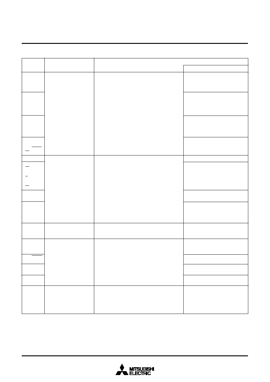
PIN DESCRIPTION
Functions
Name
Pin
∑Apply voltage of 2.7 V ≠ 5.5 V to Vcc, and 0 V to Vss.
∑In the flash memory version, apply voltage of 4.0 V ≠ 5.5 V to Vcc, and 0 V to Vss
∑This pin controls the operation mode of the chip.
∑Normally connected to V
SS
.
∑If this pin is connected to Vcc, the internal ROM is inhibited and an external memory is accessed.
∑In the flash memory version, connected to V
SS.
∑In the EPROM version or the flash memory version, this pin functions as the V
PP
power source input pin.
∑Reference voltage input pin for A-D and D-A converters.
∑Analog power source input pin for A-D and D-A converters.
∑Connect to V
SS
.
∑Reset input pin for active "L".
∑Input and output pins for the clock generating circuit.
∑Connect a ceramic resonator or quartz-crystal oscillator between the X
IN
and X
OUT
pins to set
the oscillation frequency.
∑When an external clock is used, connect the clock source to the X
IN
pin and leave the X
OUT
pin open.
∑8-bit CMOS I/O port.
∑I/O direction register allows each pin to be individually
programmed as either input or output.
∑When the external memory is used, these pins are used as the address bus.
∑CMOS compatible input level.
∑CMOS 3-state output structure or N-channel open-drain output structure.
∑8-bit CMOS I/O port.
∑I/O direction register allows each pin to be individually programmed as either input or output.
∑When the external memory is used, these pins are used as the address bus.
∑CMOS compatible input level.
∑CMOS 3-state output structure or N-channel open-drain output structure.
∑8-bit CMOS I/O port.
∑I/O direction register allows each pin to be individually programmed as either input or output.
∑When the external memory is used, these pins are used as the data bus.
∑CMOS compatible input level.
∑CMOS 3-state output structure.
∑P2
4
to P2
7
(4 bits) are enabled to output large current for LED drive (only in single-chip mode).
∑8-bit CMOS I/O port.
∑I/O direction register allows each pin to be individually
programmed as either input or output.
∑When the external memory is used, these pins are
used as the control bus.
∑CMOS compatible input level.
∑CMOS 3-state output structure.
∑These pins function as key-on wake-up and compara-
tor input.
∑These pins are enabled to control pull-up.
Power source
Table 1 Pin description (1)
Function except a port function
∑Comparator reference power source
input pin
∑Key-on wake-up input pin
∑Comparator input pin
∑PWM output pin
∑Key-on wake-up input pin
∑Comparator input pin
Reference voltage
Analog power source
Clock input
Clock output
I/O port P0
I/O port P1
I/O port P2
V
REF
AV
SS
P3
0
/PWM
00
P3
1
/PWM
10
CNV
SS
input
CNV
SS
RESET
Reset input
X
IN
X
OUT
P0
0
/P3
REF
P0
1
≠P0
7
P1
0
≠P1
7
P2
0
≠P2
7
I/O port P3
P3
2
≠P3
7
6
3886 Group
SINGLE-CHIP 8-BIT CMOS MICROCOMPUTER
MITSUBISHI MICROCOMPUTERS
P5
1
/INT
20
/S
0
P5
2
/INT
30
/R
P5
3
/INT
40
/W
Functions
Name
Pin
P4
0
/X
COUT
P4
1
/X
CIN
I/O port P4
∑8-bit I/O port with the same function as port P0.
<Input level>
P4
0
, P4
1
: CMOS input level
P4
2
≠P4
6
: CMOS compatible input level or TTL in-
put level
P4
7
: CMOS compatible input level or TTL input
level in the bus interface function
<Output structure>
P4
0
, P4
1
, P4
7
: CMOS 3-state output structure
P4
2
≠P4
6
: CMOS 3-state output structure or N-
channel open-drain output structure
∑Regardless of input or output port, P4
2
to P4
6
can
be input every pin level.
∑When P4
2
and P4
3
are used as output port, the
function which makes P4
2
and P4
3
clear to "0"
when the host CPU reads the output data bus
buffer 0 can be added.
∑8-bit I/O port with the same function as port P0.
∑CMOS compatible input level.
∑CMOS 3-state output structure.
∑P5
0
to P5
3
can be switched between CMOS com-
patible input level or TTL input level in the bus
interface function.
Function except a port function
Table 2 Pin description (2)
∑Sub-clock generating circuit I/O
pins
(Connect a resonator.)
P4
2
/INT
0
/OBF
00
P4
3
/INT
1
/OBF
01
P4
4
/RxD
P4
5
/TxD
P4
6
/S
CLK1
/OBF
10
P4
7
/S
RDY1
/S
1
P5
0
/A
0
P5
4
/CNTR
0
P5
5
/CNTR
1
P5
6
/DA
1
/PWM
01
P5
7
/DA
2
/PWM
11
P6
0
/AN
0
≠
P6
7
/AN
7
P7
0
/S
IN2
P7
1
/S
OUT2
P7
2
/S
CLK2
P7
3
/S
RDY2
/INT
21
P7
4
/INT
31
P7
5
/INT
41
P7
6
/S
DA
P7
7
/S
CL
P8
0
/DQ
0
≠
P8
7
/DQ
7
I/O port P5
I/O port P6
I/O port P7
I/O port P8
∑8-bit I/O port with the same function as port P0.
∑CMOS compatible input level.
∑CMOS 3-state output structure.
∑8-bit I/O port with the same function as port P0.
P7
0
≠P7
5
: CMOS compatible input level or TTL in-
put level
P7
6
, P7
7
: C M O S c o m p a t i b l e i n p u t l e v e l o r
SMBUS input level in the I
2
C-BUS inter-
face function, N-channel open-drain
output structure
∑Regardless of input or output port, P7
0
to P7
5
can
be input every pin level.
∑8-bit I/O port with the same function as port P0.
∑CMOS compatible input level.
∑CMOS 3-state output structure.
∑CMOS compatible input level or TTL input level in
the bus interface function.
∑Interrupt input pins
∑Bus interface function pins
∑Serial I/O1 function pins
∑Serial I/O1 function pins
∑Bus interface function pins
∑Bus interface function pins
∑Interrupt input pins
∑Bus interface function pins
∑Timer X, timer Y function pins
∑D-A converter output pin
∑PWM output pin
∑A-D converter output pin
∑Serial I/O2 function pin
∑Serial I/O2 function pin
∑Interrupt input pin
∑Interrupt input pin
∑I
2
C-BUS interface function pin
∑Bus interface function pin
7
3886 Group
SINGLE-CHIP 8-BIT CMOS MICROCOMPUTER
MITSUBISHI MICROCOMPUTERS
PART NUMBERING
Fig. 5 Part numbering
M
3
8
8
6
7
M
8
A
-
X
X
X
H
P
P
r
o
d
u
c
t
n
a
m
e
P
a
c
k
a
g
e
t
y
p
e
H
P
:
8
0
P
6
Q
-
A
G
P
:
8
0
P
6
S
-
A
F
S
:
8
0
D
0
R
O
M
n
u
m
b
e
r
O
m
i
t
t
e
d
i
n
t
h
e
o
n
e
t
i
m
e
P
R
O
M
v
e
r
s
i
o
n
s
h
i
p
p
e
d
i
n
b
l
a
n
k
,
t
h
e
E
P
R
O
M
v
e
r
s
i
o
n
a
n
d
t
h
e
f
l
a
s
h
m
e
m
o
r
y
v
e
r
s
i
o
n
.
R
O
M
/
P
R
O
M
s
i
z
e
1
2
3
4
5
6
7
8
:
4
0
9
6
b
y
t
e
s
:
8
1
9
2
b
y
t
e
s
:
1
2
2
8
8
b
y
t
e
s
:
1
6
3
8
4
b
y
t
e
s
:
2
0
4
8
0
b
y
t
e
s
:
2
4
5
7
6
b
y
t
e
s
:
2
8
6
7
2
b
y
t
e
s
:
3
2
7
6
8
b
y
t
e
s
T
h
e
f
i
r
s
t
1
2
8
b
y
t
e
s
a
n
d
t
h
e
l
a
s
t
2
b
y
t
e
s
o
f
R
O
M
a
r
e
r
e
s
e
r
v
e
d
a
r
e
a
s
;
t
h
e
y
c
a
n
n
o
t
b
e
u
s
e
d
.
H
o
w
e
v
e
r
,
t
h
e
y
c
a
n
b
e
p
r
o
g
r
a
m
m
e
d
o
r
e
r
a
s
e
d
i
n
t
h
e
E
P
R
O
M
v
e
r
s
i
o
n
a
n
d
t
h
e
f
l
a
s
h
m
e
m
o
r
y
v
e
r
s
i
o
n
,
s
o
t
h
a
t
t
h
e
u
s
e
r
s
c
a
n
u
s
e
t
h
e
m
.
M
e
m
o
r
y
t
y
p
e
M
E
F
:
M
a
s
k
R
O
M
v
e
r
s
i
o
n
:
E
P
R
O
M
o
r
O
n
e
T
i
m
e
P
R
O
M
v
e
r
s
i
o
n
:
F
l
a
s
h
m
e
m
o
r
y
v
e
r
s
i
o
n
R
A
M
s
i
z
e
0
1
2
3
4
:
1
9
2
b
y
t
e
s
:
2
5
6
b
y
t
e
s
:
3
8
4
b
y
t
e
s
:
5
1
2
b
y
t
e
s
:
6
4
0
b
y
t
e
s
A
≠
:
H
i
g
h
-
s
p
e
e
d
v
e
r
s
i
o
n
≠
i
s
o
m
i
t
t
e
d
i
n
t
h
e
O
n
e
T
i
m
e
P
R
O
M
v
e
r
s
i
o
n
s
h
i
p
p
e
d
i
n
b
l
a
n
k
,
t
h
e
E
P
R
O
M
v
e
r
s
i
o
n
a
n
d
t
h
e
f
l
a
s
h
m
e
m
o
r
y
v
e
r
s
i
o
n
.
9:
3
6
8
6
4
b
y
t
e
s
:
4
0
9
6
0
b
y
t
e
s
:
4
5
0
5
6
b
y
t
e
s
:
4
9
1
5
2
b
y
t
e
s
:
5
3
2
4
8
b
y
t
e
s
:
5
7
3
4
4
b
y
t
e
s
:
6
1
4
4
0
b
y
t
e
s
A
B
C
D
E
F
5
6
7
8
9
:
7
6
8
b
y
t
e
s
:
8
9
6
b
y
t
e
s
:
1
0
2
4
b
y
t
e
s
:
1
5
3
6
b
y
t
e
s
:
2
0
4
8
b
y
t
e
s
8
3886 Group
SINGLE-CHIP 8-BIT CMOS MICROCOMPUTER
MITSUBISHI MICROCOMPUTERS
GROUP EXPANSION
Mitsubishi plans to expand the 3886 group as follows.
Memory Type
Support for mask ROM, One Time PROM, EPROM and flash
memory version.
Memory Size
ROM size ........................................................... 32 K to 60 K bytes
RAM size .......................................................... 1024 to 2048 bytes
Packages
80P6Q-A .................................. 0.5 mm-pitch plastic molded LQFP
80P6S-A ................................... 0.65mm pitch plastic molded QFP
80D0 ....................... 0.8 mm-pitch ceramic LCC (EPROM version)
The pin number and the position of the function pin may change
by the kind of package.
Fig. 6 Memory expansion plan
Currently products are listed below.
RAM size (bytes)
Remarks
Package
Table 3 Support products
Product name
As of Jan. 2000
32768 (32638)
49152 (19022)
61440 (61310)
(P) ROM size (bytes)
ROM size for User in ( )
Memory Expansion
M38867M8A-XXXHP
M38867E8A-XXXHP
M38867E8AHP
M38867E8AFS
M38869M8A-XXXHP
M38869M8A-XXXGP
M38869MCA-XXXHP
M38869MCA-XXXGP
M38869MFA-XXXHP
M38869MFA-XXXGP
M38869FFAHP
M38869FFAGP
1024
2048
80P6Q-A
80D0
80P6Q-A
80P6S-A
80P6Q-A
80P6S-A
80P6Q-A
80P6S-A
80P6Q-A
80P6S-A
Mask ROM version
One Time PROM version
One Time PROM version (blank)
EPROM version
Mask ROM version
Flash memory version
M
3
8
8
6
7
E
8
A
/
M
8
A
4
8
K
R
O
M
s
i
z
e
(
b
y
t
e
s
)
3
2
K
2
8
K
2
4
K
2
0
K
1
6
K
1
2
K
8
K
3
8
4
5
1
2
6
4
0
1
4
0
8
7
6
8
8
9
6
1
0
2
4
1
1
5
2
1
2
8
0
1
5
3
6
2
0
4
8
3
0
7
2
4
0
3
2
6
0
K
R
O
M
e
x
t
e
r
n
a
l
R
A
M
s
i
z
e
(
b
y
t
e
s
)
:
M
a
s
s
p
r
o
d
u
c
t
i
o
n
M
3
8
8
6
9
F
F
A
/
M
F
A
M
3
8
8
6
9
M
C
A
M
3
8
8
6
9
M
8
A

9
3886 Group
SINGLE-CHIP 8-BIT CMOS MICROCOMPUTER
MITSUBISHI MICROCOMPUTERS
FUNCTIONAL DESCRIPTION
CENTRAL PROCESSING UNIT (CPU)
The 3886 group uses the standard 740 Family instruction set. Re-
fer to the table of 740 Family addressing modes and machine
instructions or the 740 Family Software Manual for details on the
instruction set.
Machine-resident 740 Family instructions are as follows:
The FST and SLW instructions cannot be used.
The STP, WIT, MUL, and DIV instructions can be used.
[CPU Mode Register (CPUM)] 003B
16
The CPU mode register contains the stack page selection bit, the
processor mode bits specifying the chip operation mode, etc.
The CPU mode register is allocated at address 003B
16
.
Fig. 7 Structure of CPU mode register
C
P
U
m
o
d
e
r
e
g
i
s
t
e
r
(
C
P
U
M
:
a
d
d
r
e
s
s
0
0
3
B
1
6
)
b
7
b
0
S
t
a
c
k
p
a
g
e
s
e
l
e
c
t
i
o
n
b
i
t
0
:
0
p
a
g
e
1
:
1
p
a
g
e
R
e
s
e
r
v
e
d
(
D
o
n
o
t
w
r
i
t
e
"
0
"
t
o
t
h
i
s
b
i
t
w
h
e
n
u
s
i
n
g
X
C
I
N
≠
X
C
O
U
T
o
s
c
i
l
l
a
t
i
o
n
f
u
n
c
t
i
o
n
.
)
P
r
o
c
e
s
s
o
r
m
o
d
e
b
i
t
s
b
1
b
0
0
0
:
S
i
n
g
l
e
-
c
h
i
p
m
o
d
e
0
1
:
M
e
m
o
r
y
e
x
p
a
n
s
i
o
n
m
o
d
e
(N
o
t
e)
1
0
:
M
i
c
r
o
p
r
o
c
e
s
s
o
r
m
o
d
e
(N
o
t
e)
1
1
:
N
o
t
a
v
a
i
l
a
b
l
e
P
o
r
t
X
C
s
w
i
t
c
h
b
i
t
0
:
I
/
O
p
o
r
t
f
u
n
c
t
i
o
n
(
s
t
o
p
o
s
c
i
l
l
a
t
i
n
g
)
1
:
X
C
I
N
≠
X
C
O
U
T
o
s
c
i
l
l
a
t
i
n
g
f
u
n
c
t
i
o
n
M
a
i
n
c
l
o
c
k
(
X
I
N
≠
X
O
U
T
)
s
t
o
p
b
i
t
0
:
O
s
c
i
l
l
a
t
i
n
g
1
:
S
t
o
p
p
e
d
M
a
i
n
c
l
o
c
k
d
i
v
i
s
i
o
n
r
a
t
i
o
s
e
l
e
c
t
i
o
n
b
i
t
s
b
7
b
6
0
0
:
=
f
(
X
I
N
)
/
2
(
h
i
g
h
-
s
p
e
e
d
m
o
d
e
)
0
1
:
=
f
(
X
I
N
)
/
8
(
m
i
d
d
l
e
-
s
p
e
e
d
m
o
d
e
)
1
0
:
=
f
(
X
C
I
N
)
/
2
(
l
o
w
-
s
p
e
e
d
m
o
d
e
)
1
1
:
N
o
t
a
v
a
i
l
a
b
l
e
N
o
t
e
:
T
h
i
s
m
o
d
e
i
s
n
o
t
a
v
a
i
l
a
b
l
e
f
o
r
M
3
8
8
6
9
M
8
A
/
M
C
A
/
M
F
A
a
n
d
t
h
e
f
l
a
s
h
m
e
m
o
r
y
v
e
r
s
i
o
n
.

10
3886 Group
SINGLE-CHIP 8-BIT CMOS MICROCOMPUTER
MITSUBISHI MICROCOMPUTERS
MEMORY
Special Function Register (SFR) Area
The Special Function Register area in the zero page contains con-
trol registers such as I/O ports and timers.
RAM
RAM is used for data storage and for stack area of subroutine
calls and interrupts.
ROM
The first 128 bytes and the last 2 bytes of ROM are reserved for
device testing and the rest is user area for storing programs. Pro-
gram/Erase of the reserved ROM area is possible in the EPROM
version and the flash memory version
Interrupt Vector Area
The interrupt vector area contains reset and interrupt vectors.
Zero Page
Access to this area with only 2 bytes is possible in the zero page
addressing mode.
Special Page
Access to this area with only 2 bytes is possible in the special
page addressing mode.
Fig. 8 Memory map diagram
0
1
0
0
1
6
0
0
0
0
1
6
0
0
4
0
1
6
F
F
0
0
1
6
F
F
D
C
1
6
F
F
F
E
1
6
F
F
F
F
1
6
1
9
2
2
5
6
3
8
4
5
1
2
6
4
0
7
6
8
8
9
6
1
0
2
4
1
5
3
6
2
0
4
8
X
X
X
X
1
6
0
0
F
F
1
6
0
1
3
F
1
6
0
1
B
F
1
6
0
2
3
F
1
6
0
2
B
F
1
6
0
3
3
F
1
6
0
3
B
F
1
6
0
4
3
F
1
6
0
6
3
F
1
6
0
8
3
F
1
6
4
0
9
6
8
1
9
2
1
2
2
8
8
1
6
3
8
4
2
0
4
8
0
2
4
5
7
6
2
8
6
7
2
3
2
7
6
8
3
6
8
6
4
4
0
9
6
0
4
5
0
5
6
4
9
1
5
2
5
3
2
4
8
5
7
3
4
4
6
1
4
4
0
F
0
0
0
1
6
E
0
0
0
1
6
D
0
0
0
1
6
C
0
0
0
1
6
B
0
0
0
1
6
A
0
0
0
1
6
9
0
0
0
1
6
8
0
0
0
1
6
7
0
0
0
1
6
6
0
0
0
1
6
5
0
0
0
1
6
4
0
0
0
1
6
3
0
0
0
1
6
2
0
0
0
1
6
1
0
0
0
1
6
F
0
8
0
1
6
E
0
8
0
1
6
D
0
8
0
1
6
C
0
8
0
1
6
B
0
8
0
1
6
A
0
8
0
1
6
9
0
8
0
1
6
8
0
8
0
1
6
7
0
8
0
1
6
6
0
8
0
1
6
5
0
8
0
1
6
4
0
8
0
1
6
3
0
8
0
1
6
2
0
8
0
1
6
1
0
8
0
1
6
Y
Y
Y
Y
1
6
Z
Z
Z
Z
1
6
R
A
M
R
O
M
0
F
F
E
1
6
0
F
F
F
1
6
S
F
R
a
r
e
a
N
o
t
u
s
e
d
I
n
t
e
r
r
u
p
t
v
e
c
t
o
r
a
r
e
a
R
O
M
a
r
e
a
R
e
s
e
r
v
e
d
R
O
M
a
r
e
a
(
N
o
t
e
2
)
(
1
2
8
b
y
t
e
s
)
Z
e
r
o
p
a
g
e
S
p
e
c
i
a
l
p
a
g
e
R
A
M
a
r
e
a
R
A
M
s
i
z
e
(
b
y
t
e
s
)
A
d
d
r
e
s
s
X
X
X
X
1
6
R
O
M
s
i
z
e
(
b
y
t
e
s
)
A
d
d
r
e
s
s
Y
Y
Y
Y
1
6
R
e
s
e
r
v
e
d
R
O
M
a
r
e
a
(
N
o
t
e
2
)
A
d
d
r
e
s
s
Z
Z
Z
Z
1
6
S
F
R
a
r
e
a (
N
o
t
e
1
)
N
o
t
e
s
1
:
T
h
i
s
a
r
e
a
i
s
S
F
R
i
n
M
3
8
8
6
9
F
F
A
.
T
h
i
s
a
r
e
a
i
s
R
e
s
e
r
v
e
d
i
n
M
3
8
8
6
9
M
F
A
/
M
C
A
/
M
8
A
.
T
h
i
s
a
r
e
a
i
s
n
o
t
u
s
e
d
i
n
M
3
8
8
6
7
M
8
A
/
E
8
A
.
2
:
T
h
i
s
a
r
e
a
i
s
u
sa
b
l
e
i
n
E
P
R
O
M
v
e
r
s
i
o
n
a
n
d
f
l
a
s
h
m
e
m
o
r
y
v
e
r
s
i
o
n
.
11
3886 Group
SINGLE-CHIP 8-BIT CMOS MICROCOMPUTER
MITSUBISHI MICROCOMPUTERS
Fig. 9 Memory map of special function register (SFR)
0
0
2
0
1
6
0
0
2
1
1
6
0
0
2
2
1
6
0
0
2
3
1
6
0
0
2
4
1
6
0
0
2
5
1
6
0
0
2
6
1
6
0
0
2
7
1
6
0
0
2
8
1
6
0
0
2
9
1
6
0
0
2
A
1
6
0
0
2
B
1
6
0
0
2
C
1
6
0
0
2
D
1
6
0
0
2
E
1
6
0
0
2
F
1
6
0
0
3
0
1
6
0
0
3
1
1
6
0
0
3
2
1
6
0
0
3
3
1
6
0
0
3
4
1
6
0
0
3
5
1
6
0
0
3
6
1
6
0
0
3
7
1
6
0
0
3
8
1
6
0
0
3
9
1
6
0
0
3
A
1
6
0
0
3
B
1
6
0
0
3
C
1
6
0
0
3
D
1
6
0
0
3
E
1
6
0
0
3
F
1
6
0
0
0
0
1
6
0
0
0
1
1
6
0
0
0
2
1
6
0
0
0
3
1
6
0
0
0
4
1
6
0
0
0
5
1
6
0
0
0
6
1
6
0
0
0
7
1
6
0
0
0
8
1
6
0
0
0
9
1
6
0
0
0
A
1
6
0
0
0
B
1
6
0
0
0
C
1
6
0
0
0
D
1
6
0
0
0
E
1
6
0
0
0
F
1
6
0
0
1
0
1
6
0
0
1
1
1
6
0
0
1
2
1
6
0
0
1
3
1
6
0
0
1
4
1
6
0
0
1
5
1
6
0
0
1
6
1
6
0
0
1
7
1
6
0
0
1
8
1
6
0
0
1
9
1
6
0
0
1
A
1
6
0
0
1
B
1
6
0
0
1
C
1
6
0
0
1
D
1
6
0
0
1
E
1
6
0
0
1
F
1
6
S
e
r
i
a
l
I
/
O
2
r
e
g
i
s
t
e
r
(
S
I
O
2
)
P
o
r
t
P
0
(
P
0
)
P
o
r
t
P
0
d
i
r
e
c
t
i
o
n
r
e
g
i
s
t
e
r
(
P
0
D
)
P
o
r
t
P
1
(
P
1
)
P
o
r
t
P
1
d
i
r
e
c
t
i
o
n
r
e
g
i
s
t
e
r
(
P
1
D
)
P
o
r
t
P
2
(
P
2
)
P
o
r
t
P
2
d
i
r
e
c
t
i
o
n
r
e
g
i
s
t
e
r
(
P
2
D
)
P
o
r
t
P
3
(
P
3
)
P
o
r
t
P
3
d
i
r
e
c
t
i
o
n
r
e
g
i
s
t
e
r
(
P
3
D
)
P
o
r
t
P
4
(
P
4
)
P
o
r
t
P
4
d
i
r
e
c
t
i
o
n
r
e
g
i
s
t
e
r
(
P
4
D
)
P
o
r
t
P
5
(
P
5
)
P
o
r
t
P
5
d
i
r
e
c
t
i
o
n
r
e
g
i
s
t
e
r
(
P
5
D
)
P
o
r
t
P
6
(
P
6
)
P
o
r
t
P
6
d
i
r
e
c
t
i
o
n
r
e
g
i
s
t
e
r
(
P
6
D
)
P
o
r
t
P
7
(
P
7
)
P
o
r
t
P
7
d
i
r
e
c
t
i
o
n
r
e
g
i
s
t
e
r
(
P
7
D
)
P
o
r
t
P
8
(
P
8
)
/
P
o
r
t
P
4
i
n
p
u
t
r
e
g
i
s
t
e
r
(
P
4
I
)
T
r
a
n
s
m
i
t
/
R
e
c
e
i
v
e
b
u
f
f
e
r
r
e
g
i
s
t
e
r
(
T
B
/
R
B
)
S
e
r
i
a
l
I
/
O
1
s
t
a
t
u
s
r
e
g
i
s
t
e
r
(
S
I
O
1
S
T
S
)
S
e
r
i
a
l
I
/
O
1
c
o
n
t
r
o
l
r
e
g
i
s
t
e
r
(
S
I
O
1
C
O
N
)
U
A
R
T
c
o
n
t
r
o
l
r
e
g
i
s
t
e
r
(
U
A
R
T
C
O
N
)
B
a
u
d
r
a
t
e
g
e
n
e
r
a
t
o
r
(
B
R
G
)
S
e
r
i
a
l
I
/
O
2
c
o
n
t
r
o
l
r
e
g
i
s
t
e
r
(
S
I
O
2
C
O
N
)
I
n
t
e
r
r
u
p
t
c
o
n
t
r
o
l
r
e
g
i
s
t
e
r
2
(
I
C
O
N
2
)
A
-
D
c
o
n
v
e
r
s
i
o
n
r
e
g
i
s
t
e
r
1
(
A
D
1
)
P
r
e
s
c
a
l
e
r
Y
(
P
R
E
Y
)
T
i
m
e
r
Y
(
T
Y
)
A
D
/
D
A
c
o
n
t
r
o
l
r
e
g
i
s
t
e
r
(
A
D
C
O
N
)
D
-
A
1
c
o
n
v
e
r
s
i
o
n
r
e
g
i
s
t
e
r
(
D
A
1
)
D
-
A
2
c
o
n
v
e
r
s
i
o
n
r
e
g
i
s
t
e
r
(
D
A
2
)
I
n
t
e
r
r
u
p
t
e
d
g
e
s
e
l
e
c
t
i
o
n
r
e
g
i
s
t
e
r
(
I
N
T
E
D
G
E
)
C
P
U
m
o
d
e
r
e
g
i
s
t
e
r
(
C
P
U
M
)
I
n
t
e
r
r
u
p
t
r
e
q
u
e
s
t
r
e
g
i
s
t
e
r
1
(
I
R
E
Q
1
)
I
n
t
e
r
r
u
p
t
r
e
q
u
e
s
t
r
e
g
i
s
t
e
r
2
(
I
R
E
Q
2
)
I
n
t
e
r
r
u
p
t
c
o
n
t
r
o
l
r
e
g
i
s
t
e
r
1
(
I
C
O
N
1
)
P
r
e
s
c
a
l
e
r
1
2
(
P
R
E
1
2
)
T
i
m
e
r
2
(
T
2
)
P
r
e
s
c
a
l
e
r
X
(
P
R
E
X
)
T
i
m
e
r
X
(
T
X
)
T
i
m
e
r
1
(
T
1
)
T
i
m
e
r
X
Y
m
o
d
e
r
e
g
i
s
t
e
r
(
T
M
)
I
2
C
d
a
t
a
s
h
i
f
t
r
e
g
i
s
t
e
r
(
S
0
)
I
2
C
a
d
d
r
e
s
s
r
e
g
i
s
t
e
r
(
S
0
D
)
I
2
C
s
t
a
t
u
s
r
e
g
i
s
t
e
r
(
S
1
)
I
2
C
c
o
n
t
r
o
l
r
e
g
i
s
t
e
r
(
S
1
D
)
I
2
C
c
l
o
c
k
c
o
n
t
r
o
l
r
e
g
i
s
t
e
r
(
S
2
)
I
2
C
s
t
a
r
t
/
s
t
o
p
c
o
n
d
i
t
i
o
n
c
o
n
t
r
o
l
r
e
g
i
s
t
e
r
(
S
2
D
)
D
a
t
a
b
a
s
b
u
f
f
e
r
r
e
g
i
s
t
e
r
0
(
D
B
B
0
)
D
a
t
a
b
a
s
b
u
f
f
e
r
s
t
a
t
u
s
r
e
g
i
s
t
e
r
0
(
D
B
B
S
T
S
0
)
D
a
t
a
b
a
s
b
u
f
f
e
r
c
o
n
t
r
o
l
r
e
g
i
s
t
e
r
(
D
B
B
C
O
N
)
D
a
t
a
b
a
s
b
u
f
f
e
r
r
e
g
i
s
t
e
r
1
(
D
B
B
1
)
D
a
t
a
b
a
s
b
u
f
f
e
r
s
t
a
t
u
s
r
e
g
i
s
t
e
r
1
(
D
B
B
S
T
S
1
)
C
o
m
p
a
r
a
t
o
r
d
a
t
a
r
e
g
i
s
t
e
r
(
C
M
P
D
)
P
o
r
t
c
o
n
t
r
o
l
r
e
g
i
s
t
e
r
1
(
P
C
T
L
1
)
P
o
r
t
c
o
n
t
r
o
l
r
e
g
i
s
t
e
r
2
(
P
C
T
L
2
)
P
W
M
0
H
r
e
g
i
s
t
e
r
(
P
W
M
0
H
)
P
W
M
0
L
r
e
g
i
s
t
e
r
(
P
W
M
0
L
)
P
W
M
1
H
r
e
g
i
s
t
e
r
(
P
W
M
1
H
)
P
W
M
1
L
r
e
g
i
s
t
e
r
(
P
W
M
1
L
)
A
-
D
c
o
n
v
e
r
s
i
o
n
r
e
g
i
s
t
e
r
2
(
A
D
2
)
I
n
t
e
r
r
u
p
t
s
o
u
r
c
e
s
e
l
e
c
t
i
o
n
r
e
g
i
s
t
e
r
(
I
N
T
S
E
L
)
W
a
t
c
h
d
o
g
t
i
m
e
r
c
o
n
t
r
o
l
r
e
g
i
s
t
e
r
(
W
D
T
C
O
N
)
0
F
F
E
1
6
0
F
F
F
1
6
F
l
a
s
h
c
o
m
m
a
n
d
r
e
g
i
s
t
e
r
(
F
C
M
D
)
F
l
a
s
h
m
e
m
o
r
y
c
o
n
t
r
o
l
r
e
g
i
s
t
e
r
(
F
C
O
N
)
(
N
o
t
e
)
(
N
o
t
e
)
N
o
t
e
:
F
l
a
s
h
m
e
m
o
r
y
v
e
r
s
i
o
n
o
n
l
y
P
o
r
t
P
8
d
i
r
e
c
t
i
o
n
r
e
g
i
s
t
e
r
(
P
8
D
)
/
P
o
r
t
P
7
i
n
p
u
t
r
e
g
i
s
t
e
r
(
P
7
I
)
12
3886 Group
SINGLE-CHIP 8-BIT CMOS MICROCOMPUTER
MITSUBISHI MICROCOMPUTERS
Pin
Name
Input/Output
I/O Structure
Non-Port Function
Ref.No.
Table 4 I/O port function (1)
Related SFRs
I/O PORTS
The I/O ports have direction registers which determine the input/
output direction of each individual pin. Each bit in a direction reg-
ister corresponds to one pin, and each pin can be set to be input
port or output port.
When "0" is written to the bit corresponding to a pin, that pin be-
comes an input pin. When "1" is written to that bit, that pin
becomes an output pin.
If data is read from a pin which is set to output, the value of the
port output latch is read, not the value of the pin itself. Pins set to
input are floating. If a pin set to input is written to, only the port
output latch is written to and the pin remains floating.
When the P8 function select bit of the port control register 2 (ad-
dress 002F
16
) is set to "1", read from address 0010
16
becomes
the port P4 input register, and read from address 0011
16
becomes
the port P7 input register.
As the particular function, value of P4
2
to P4
6
pins and P7
0
to P7
5
pins can be read regardless of setting direction registers, by read-
ing the port P4 input register (address 0010
16
) or the port P7 input
register (address 0011
16
) respectively.
P0
0
/P3
REF
P0
1
≠P0
7
P1
0
≠P1
7
P2
0
≠P2
7
P3
0
/PWM
00
P3
1
/PWM
10
P3
2
≠P3
7
P4
0
/X
COUT
P4
1
/X
CIN
P4
2
/INT
0
/
OBF
00
P4
3
/INT
1
/
OBF
01
P4
4
/R
X
D
P4
5
/T
X
D
P4
6
/S
CLK1
/OBF
10
P4
7
/S
RDY1
/S
1
Port P0
Port P1
Port P2
Port P3
Port P4
Input/output,
individual bits
CMOS compatible
input level
CMOS 3-state output
or N-channel open-
drain output
CMOS compatible
input level
CMOS 3-state output
CMOS compatible
input level or TTL
input level
CMOS 3-state output
or N-channel open-
drain output
Address low-order byte
output
A n a l o g c o m p a r a t o r
power source input pin
Address low-order byte
output
A d d r e s s h i g h - o r d e r
byte output
Data bus I/O
Control signal I/O
PWM output
Key-on wake up input
Comparator input
Control signal I/O
Key-on wake up input
Comparator input
Sub-clock generating
circuit
External interrupt input
Bus interface function
I/O
Serial I/O1 function in-
put
Serial I/O1 function out-
put
Serial I/O1 function I/O
Bus interface function
output
Serial I/O1 function out-
put
Bus interface function
input
CPU mode register
Port control register 1
Serial I/O2 control
register
CPU mode register
Port control register 1
CPU mode register
CPU mode register
Port control register 1
AD/DA control register
CPU mode register
Port control register 1
CPU mode register
Interrupt edge selection
register
Port control register 2
Serial I/O1 control
register
Port control register 2
Serial I/O1 control
register
UART control register
Port control register 2
Serial I/O1 control
register
Data bus buffer control
register
Port control register 2
Serial I/O1 control
register
Data bus buffer control
register
(1)
(2)
(3)
(4)
(5)
(6)
(7)
(8)
(9)
(10)
(11)
(12)
(13)
(14)
CMOS compatible
input level
CMOS 3-state output
(when selecting bus
interface function)
CMOS compatible
input level or TTL
input level
13
3886 Group
SINGLE-CHIP 8-BIT CMOS MICROCOMPUTER
MITSUBISHI MICROCOMPUTERS
Notes1: For details of the functions of ports P0 to P3 in modes other than single-chip mode, and how to use double-function ports as function I/O ports, refer
to the applicable sections.
2: Make sure that the input level at each pin is either 0 V or V
CC
during execution of the STP instruction.
When an input level is at an intermediate potential, a current will flow from V
CC
to V
SS
through the input-stage gate.
Pin
Name
Input/Output
I/O Format
Non-Port Function
Ref.No.
Table 5 I/O port function (2)
Related SFRs
P5
0
/A
0
P5
1
/INT
20
/S
0
P5
2
/INT
30
/R
P5
3
/INT
40
/W
P5
4
/CNTR
0
P5
5
/CNTR
1
P5
6
/DA
1
/
PWM
01
P5
7
/DA
2
/
PWM
11
P6
0
/AN
0
≠
P6
7
/AN
7
P7
0
/S
IN2
P7
1
/S
OUT2
P7
2
/S
CLK2
P7
3
/S
RDY2
/
INT
21
P7
4
/INT
31
P7
5
/INT
41
P7
6
/S
DA
P7
7
/S
CL
P8
0
/DQ
0
≠
P8
7
/DQ
7
Port P5
Port P6
Port P7
Port P8
Input/output,
individual bits
CMOS compatible
input level
CMOS 3-state output
(when selecting bus
interface function)
CMOS compatible
input level or TTL
input level
CMOS compatible
input level
CMOS 3-state output
CMOS compatible
input level or TTL
input level
N-channel open-drain
output
CMOS compatible
input level
N-channel open-drain
output
(when selecting I
2
C-
BUS interface
function)
CMOS compatible
input level or SMBUS
input level
CMOS compatible
input level
CMOS 3-state output
(when selecting bus
interface function)
CMOS compatible
input level or TTL
input level
Bus interface function
input
External interrupt input
Bus interface function
input
Timer X, timer Y func-
tion I/O
D-A converter output
PWM output
A-D converter input
Serial I/O2 function I/O
Serial I/O2 function out-
put
Bus interface function
input
External interrupt input
I
2
C-BUS interface func-
tion I/O
Bus interface function
I/O
Data bus buffer control
register
Interrupt edge selection
register
Data bus buffer control
register
Timer XY mode register
AD/DA control register
UART control register
AD/DA control register
Serial I/O2 control
register
Port control register 2
Serial I/O2 control
register
Port control register 2
Interrupt edge selection
register
Port control register 2
I
2
C control register
Data bus buffer control
register
(15)
(16)
(17)
(18)
(19)
(20)
(21)
(22)
(23)
(24)
(25)
(26)
(27)
(28)
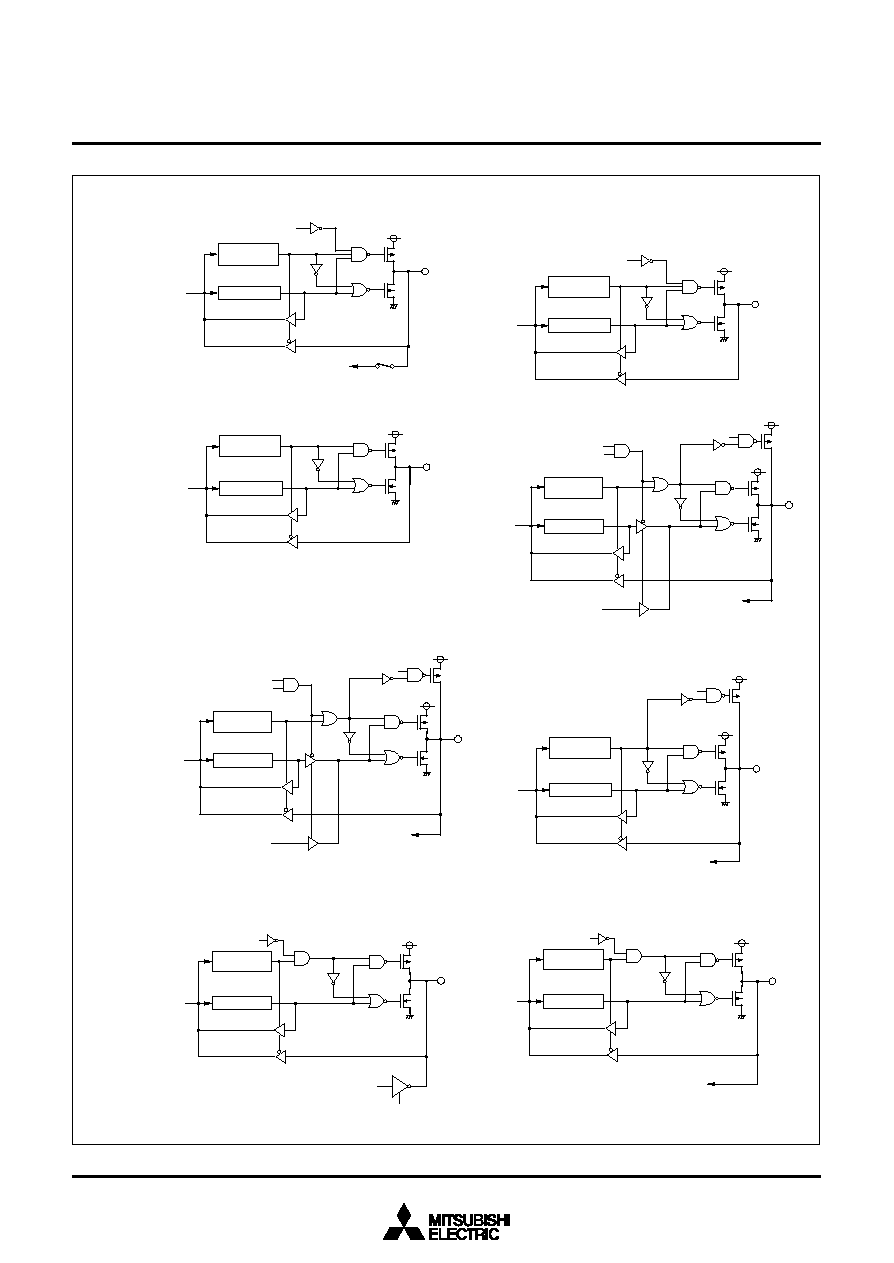
14
3886 Group
SINGLE-CHIP 8-BIT CMOS MICROCOMPUTER
MITSUBISHI MICROCOMPUTERS
Fig. 10 Port block diagram (1)
(
2
)
P
o
r
t
s
P
0
1
≠
P
0
7
,
P
1
D
a
t
a
b
u
s
P
o
r
t
l
a
t
c
h
o
u
t
p
u
t
s
t
r
u
c
t
u
r
e
s
e
l
e
c
t
i
o
n
b
i
t
s
(
3
)
P
o
r
t
P
2
D
a
t
a
b
u
s
P
o
r
t
l
a
t
c
h
(
4
)
P
o
r
t
P
3
0
C
o
m
p
a
r
a
t
o
r
K
e
y
-
o
n
w
a
k
e
-
u
p
P
3
0
≠
P
3
3
p
u
l
l
-
u
p
c
o
n
t
r
o
l
b
i
t
i
n
p
u
t
D
a
t
a
b
u
s
P
o
r
t
l
a
t
c
h
P
W
M
0
0
o
u
t
p
u
t
P
W
M
0
o
u
t
p
u
t
p
i
n
s
e
l
e
c
t
i
o
n
b
i
t
P
W
M
0
e
n
a
b
l
e
b
i
t
(
5
)
P
o
r
t
P
3
1
P
3
0
≠
P
3
3
p
u
l
l
-
u
p
c
o
n
t
r
o
l
b
i
t
D
a
t
a
b
u
s
P
o
r
t
l
a
t
c
h
P
W
M
1
0
o
u
t
p
u
t
P
W
M
1
o
u
t
p
u
t
p
i
n
s
e
l
e
c
t
i
o
n
b
i
t
P
W
M
1
e
n
a
b
l
e
b
i
t
(
6
)
P
o
r
t
s
P
3
2
≠
P
3
7
(
7
)
P
o
r
t
P
4
0
P
o
r
t
X
C
s
w
i
t
c
h
b
i
t
O
s
c
i
l
l
a
t
o
r
P
o
r
t
P
4
1
P
o
r
t
X
C
s
w
i
t
c
h
b
i
t
(
8
)
P
o
r
t
P
4
1
S
u
b
-
c
l
o
c
k
g
e
n
e
r
a
t
i
n
g
c
i
r
c
u
i
t
i
n
p
u
t
(
1
)
P
o
r
t
P
0
0
D
a
t
a
b
u
s
P
o
r
t
l
a
t
c
h
P
0
0
≠
P
0
3
o
u
t
p
u
t
s
t
r
u
c
t
u
r
e
s
e
l
e
c
t
i
o
n
b
i
t
C
o
m
p
a
r
a
t
o
r
r
e
f
e
r
e
n
c
e
p
o
w
e
r
s
o
u
r
c
e
i
n
p
u
t
C
o
m
p
a
r
a
t
o
r
r
e
f
e
r
e
n
c
e
i
n
p
u
t
p
i
n
s
e
l
e
c
t
b
i
t
P
0
0
≠
P
0
3
,
P
0
4
≠
P
0
7
,
P
1
0
≠
P
1
3
,
P
1
4
≠
P
1
7
p
u
l
l
-
u
p
c
o
n
t
r
o
l
b
i
t
P
3
0
≠
P
3
3
,
P
3
4
≠
P
3
7
C
o
m
p
a
r
a
t
o
r
K
e
y
-
o
n
w
a
k
e
-
u
p
i
n
p
u
t
D
a
t
a
b
u
s
P
o
r
t
l
a
t
c
h
C
o
m
p
a
r
a
t
o
r
K
e
y
-
o
n
w
a
k
e
-
u
p
i
n
p
u
t
D
a
t
a
b
u
s
P
o
r
t
l
a
t
c
h
P
o
r
t
X
C
s
w
i
t
c
h
b
i
t
D
a
t
a
b
u
s
P
o
r
t
l
a
t
c
h
D
i
r
e
c
t
i
o
n
r
e
g
i
s
t
e
r
D
i
r
e
c
t
i
o
n
r
e
g
i
s
t
e
r
D
i
r
e
c
t
i
o
n
r
e
g
i
s
t
e
r
D
i
r
e
c
t
i
o
n
r
e
g
i
s
t
e
r
D
i
r
e
c
t
i
o
n
r
e
g
i
s
t
e
r
D
i
r
e
c
t
i
o
n
r
e
g
i
s
t
e
r
D
i
r
e
c
t
i
o
n
r
e
g
i
s
t
e
r
D
i
r
e
c
t
i
o
n
r
e
g
i
s
t
e
r

15
3886 Group
SINGLE-CHIP 8-BIT CMOS MICROCOMPUTER
MITSUBISHI MICROCOMPUTERS
Fig. 11 Port block diagram (2)
S
e
r
i
a
l
I
/
O
1
i
n
p
u
t
(
1
1
)
P
o
r
t
P
4
4
D
a
t
a
b
u
s
S
e
r
i
a
l
I
/
O
1
e
n
a
b
l
e
b
i
t
R
e
c
e
i
v
e
e
n
a
b
l
e
b
i
t
P
o
r
t
l
a
t
c
h
P
4
o
u
t
p
u
t
s
t
r
u
c
t
u
r
e
s
e
l
e
c
t
i
o
n
b
i
t
T
1
(
1
2
)
P
o
r
t
P
4
5
D
a
t
a
b
u
s
S
e
r
i
a
l
I
/
O
1
e
n
a
b
l
e
b
i
t
T
r
a
n
s
m
i
t
e
n
a
b
l
e
b
i
t
S
e
r
i
a
l
I
/
O
1
o
u
t
p
u
t
P
4
5
/
T
X
D
P
-
c
h
a
n
n
e
l
o
u
t
p
u
t
d
i
s
a
b
l
e
b
i
t
P
o
r
t
l
a
t
c
h
(
1
3
)
P
o
r
t
P
4
6
S
e
r
i
a
l
I
/
O
1
s
y
n
c
h
r
o
n
o
u
s
c
l
o
c
k
s
e
l
e
c
t
i
o
n
b
i
t
D
a
t
a
b
u
s
S
e
r
i
a
l
I
/
O
1
c
l
o
c
k
o
u
t
p
u
t
S
e
r
i
a
l
I
/
O
1
e
x
t
e
r
n
a
l
c
l
o
c
k
i
n
p
u
t
S
e
r
i
a
l
I
/
O
1
m
o
d
e
s
e
l
e
c
t
i
o
n
b
i
t
S
e
r
i
a
l
I
/
O
1
e
n
a
b
l
e
b
i
t
P
o
r
t
l
a
t
c
h
S
e
r
i
a
l
I
/
O
1
e
n
a
b
l
e
b
i
t
O
B
F
1
0
o
u
t
p
u
t
e
n
a
b
l
e
b
i
t
O
B
F
1
0
o
u
t
p
u
t
P
4
o
u
t
p
u
t
s
t
r
u
c
t
u
r
e
s
e
l
e
c
t
i
o
n
b
i
t
(
1
4
)
P
o
r
t
P
4
7
(
1
5
)
P
o
r
t
P
5
0
(
1
6
)
P
o
r
t
s
P
5
1
,
P
5
2
,
P
5
3
T
1
. T
h
e
i
n
p
u
t
l
e
v
e
l
c
a
n
b
e
s
w
i
t
c
h
e
d
b
e
t
w
e
e
n
C
M
O
S
c
o
m
p
a
t
i
b
l
e
i
n
p
u
t
l
e
v
e
l
a
n
d
T
T
L
l
e
v
e
l
b
y
t
h
e
P
4
i
n
p
u
t
l
e
v
e
l
s
e
l
e
c
t
i
o
n
b
i
t
o
f
t
h
e
p
o
r
t
c
o
n
t
r
o
l
r
e
g
i
s
t
e
r
2
(
a
d
d
r
e
s
s
0
0
2
F
1
6
)
.
T
2
. T
h
e
i
n
p
u
t
l
e
v
e
l
c
a
n
b
e
s
w
i
t
c
h
e
d
b
e
t
w
e
e
n
C
M
O
S
c
o
m
p
a
t
i
b
l
e
i
n
p
u
t
l
e
v
e
l
a
n
d
T
T
L
l
e
v
e
l
b
y
t
h
e
P
4
i
n
p
u
t
l
e
v
e
l
s
e
l
e
c
t
i
o
n
b
i
t
o
f
t
h
e
p
o
r
t
c
o
n
t
r
o
l
r
e
g
i
s
t
e
r
2
(
a
d
d
r
e
s
s
0
0
2
F
1
6
)
.
T
h
e
p
o
r
t
P
8
a
n
d
p
o
r
t
P
4
i
n
p
u
t
r
e
g
i
s
t
e
r
c
a
n
b
e
s
w
i
t
c
h
e
d
b
y
t
h
e
P
8
f
u
n
c
t
i
o
n
s
e
l
e
c
t
i
o
n
b
i
t
o
f
t
h
e
p
o
r
t
c
o
n
t
r
o
l
r
e
g
i
s
t
e
r
2
(
a
d
d
r
e
s
s
0
0
2
F
1
6
)
.
T
3
. T
h
e
i
n
p
u
t
l
e
v
e
l
c
a
n
b
e
s
w
i
t
c
h
e
d
b
e
t
w
e
e
n
C
M
O
S
c
o
m
p
a
t
i
b
l
e
i
n
p
u
t
l
e
v
e
l
a
n
d
T
T
L
l
e
v
e
l
b
y
t
h
e
i
n
p
u
t
l
e
v
e
l
s
e
l
e
c
t
i
o
n
b
i
t
o
f
t
h
e
d
a
t
a
b
u
s
b
u
f
f
e
r
c
o
n
t
r
o
l
r
e
g
i
s
t
e
r
(
a
d
d
r
e
s
s
0
0
2
A
1
6
)
.
(
9
)
P
o
r
t
P
4
2
O
B
F
0
0
o
u
t
p
u
t
e
n
a
b
l
e
b
i
t
O
B
F
0
0
o
u
t
p
u
t
P
4
o
u
t
p
u
t
s
t
r
u
c
t
u
r
e
s
e
l
e
c
t
i
o
n
b
i
t
I
N
T
0
i
n
t
e
r
r
u
p
t
i
n
p
u
t
(
1
0
)
P
o
r
t
P
4
3
O
B
F
0
1
o
u
t
p
u
t
e
n
a
b
l
e
b
i
t
O
B
F
0
1
o
u
t
p
u
t
D
a
t
a
b
u
s
P
o
r
t
l
a
t
c
h
D
i
r
e
c
t
i
o
n
r
e
g
i
s
t
e
r
T
1
P
4
o
u
t
p
u
t
s
t
r
u
c
t
u
r
e
s
e
l
e
c
t
i
o
n
b
i
t
I
N
T
1
i
n
t
e
r
r
u
p
t
i
n
p
u
t
D
a
t
a
b
u
s
P
o
r
t
l
a
t
c
h
D
a
t
a
b
u
s
b
u
f
f
e
r
e
n
a
b
l
e
b
i
t
I
N
T
2
0
,
I
N
T
3
0
,
I
N
T
4
0
i
n
t
e
r
r
u
p
t
i
n
p
u
t
S
0
,
R
,
W
i
n
p
u
t
D
a
t
a
b
u
s
P
o
r
t
l
a
t
c
h
D
a
t
a
b
u
s
b
u
f
f
e
r
e
n
a
b
l
e
b
i
t
A
0
i
n
p
u
t
D
a
t
a
b
u
s
b
u
f
f
e
r
e
n
a
b
l
e
b
i
t
D
a
t
a
b
u
s
b
u
f
f
e
r
e
n
a
b
l
e
b
i
t
S
e
r
i
a
l
I
/
O
1
m
o
d
e
s
e
l
e
c
t
i
o
n
b
i
t
S
e
r
i
a
l
I
/
O
1
e
n
a
b
l
e
b
i
t
S
R
D
Y
1
o
u
t
p
u
t
e
n
a
b
l
e
b
i
t
D
a
t
a
b
u
s
S
e
r
i
a
l
I
/
O
1
r
e
a
d
y
o
u
t
p
u
t
P
o
r
t
l
a
t
c
h
D
a
t
a
b
u
s
b
u
f
f
e
r
f
u
n
c
t
i
o
n
s
e
l
e
c
t
i
o
n
b
i
t
S
1
i
n
p
u
t
T
3
D
a
t
a
b
u
s
b
u
f
f
e
r
f
u
n
c
t
i
o
n
s
e
l
e
c
t
i
o
n
b
i
t
T
2
T
2
D
a
t
a
b
u
s
P
o
r
t
l
a
t
c
h
D
i
r
e
c
t
i
o
n
r
e
g
i
s
t
e
r
T
1
T
2
D
i
r
e
c
t
i
o
n
r
e
g
i
s
t
e
r
D
i
r
e
c
t
i
o
n
r
e
g
i
s
t
e
r
T
1
T
2
T
1
T
2
D
i
r
e
c
t
i
o
n
r
e
g
i
s
t
e
r
D
i
r
e
c
t
i
o
n
r
e
g
i
s
t
e
r
D
i
r
e
c
t
i
o
n
r
e
g
i
s
t
e
r
T
3
D
i
r
e
c
t
i
o
n
r
e
g
i
s
t
e
r
T
3
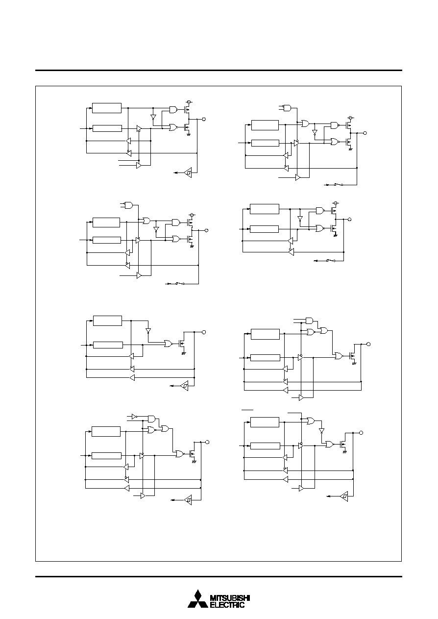
16
3886 Group
SINGLE-CHIP 8-BIT CMOS MICROCOMPUTER
MITSUBISHI MICROCOMPUTERS
Fig. 12 Port block diagram (3)
(
2
0
)
P
o
r
t
P
6
A
n
a
l
o
g
i
n
p
u
t
p
i
n
s
e
l
e
c
t
i
o
n
b
i
t
A
-
D
c
o
n
v
e
r
t
e
r
i
n
p
u
t
D
a
t
a
b
u
s
P
o
r
t
l
a
t
c
h
D
i
r
e
c
t
i
o
n
r
e
g
i
s
t
e
r
(
1
8
)
P
o
r
t
P
5
6
D
-
A
c
o
n
v
e
r
t
e
r
o
u
t
p
u
t
D
-
A
1
o
u
t
p
u
t
e
n
a
b
l
e
b
i
t
D
a
t
a
b
u
s
P
o
r
t
l
a
t
c
h
D
i
r
e
c
t
i
o
n
r
e
g
i
s
t
e
r
P
W
M
0
1
o
u
t
p
u
t
P
W
M
0
o
u
t
p
u
t
p
i
n
s
e
l
e
c
t
i
o
n
b
i
t
P
W
M
0
e
n
a
b
l
e
b
i
t
(
1
9
)
P
o
r
t
P
5
7
D
-
A
c
o
n
v
e
r
t
e
r
o
u
t
p
u
t
D
-
A
2
o
u
t
p
u
t
e
n
a
b
l
e
b
i
t
D
a
t
a
b
u
s
P
o
r
t
l
a
t
c
h
D
i
r
e
c
t
i
o
n
r
e
g
i
s
t
e
r
P
W
M
1
1
o
u
t
p
u
t
P
W
M
1
o
u
t
p
u
t
p
i
n
s
e
l
e
c
t
i
o
n
b
i
t
P
W
M
1
e
n
a
b
l
e
b
i
t
(
1
7
)
P
o
r
t
s
P
5
4
,
P
5
5
P
o
r
t
l
a
t
c
h
D
a
t
a
b
u
s
P
u
l
s
e
o
u
t
p
u
t
m
o
d
e
T
i
m
e
r
o
u
t
p
u
t
C
N
T
R
0
,
C
N
T
R
1
i
n
t
e
r
r
u
p
t
i
n
p
u
t
D
i
r
e
c
t
i
o
n
r
e
g
i
s
t
e
r
(
2
1
)
P
o
r
t
P
7
0
S
e
r
i
a
l
I
/
O
2
i
n
p
u
t
D
a
t
a
b
u
s
P
o
r
t
l
a
t
c
h
D
i
r
e
c
t
i
o
n
r
e
g
i
s
t
e
r
T
4
(
2
2
)
P
o
r
t
P
7
1
D
a
t
a
b
u
s
P
o
r
t
l
a
t
c
h
D
i
r
e
c
t
i
o
n
r
e
g
i
s
t
e
r
S
e
r
i
a
l
I
O
/
2
t
r
a
n
s
m
i
t
c
o
m
p
l
e
t
i
o
n
s
i
g
n
a
l
S
e
r
i
a
l
I
/
O
2
p
o
r
t
s
e
l
e
c
t
i
o
n
b
i
t
S
e
r
i
a
l
I
/
O
2
o
u
t
p
u
t
(
2
3
)
P
o
r
t
P
7
2
D
a
t
a
b
u
s
P
o
r
t
l
a
t
c
h
D
i
r
e
c
t
i
o
n
r
e
g
i
s
t
e
r
S
e
r
i
a
l
I
/
O
2
s
y
n
c
h
r
o
n
i
z
a
t
i
o
n
c
l
o
c
k
s
e
l
e
c
t
i
o
n
b
i
t
S
e
r
i
a
l
I
/
O
2
p
o
r
t
s
e
l
e
c
t
i
o
n
b
i
t
S
e
r
i
a
l
I
/
O
2
c
l
o
c
k
o
u
t
p
u
t
S
e
r
i
a
l
I
/
O
2
e
x
t
e
r
n
a
l
c
l
o
c
k
i
n
p
u
t
T
4
.
T
h
e
i
n
p
u
t
l
e
v
e
l
c
a
n
b
e
s
w
i
t
c
h
e
d
b
e
t
w
e
e
n
C
M
O
S
c
o
m
p
a
t
i
b
l
e
i
n
p
u
t
l
e
v
e
l
a
n
d
T
T
L
l
e
v
e
l
b
y
t
h
e
P
7
i
n
p
u
t
l
e
v
e
l
s
e
l
e
c
t
i
o
n
b
i
t
o
f
t
h
e
p
o
r
t
c
o
n
t
r
o
l
r
e
g
i
s
t
e
r
2
(
a
d
d
r
e
s
s
0
0
2
F
1
6
)
.
T
5
.
T
h
e
i
n
p
u
t
l
e
v
e
l
c
a
n
b
e
s
w
i
t
c
h
e
d
b
e
t
w
e
e
n
C
M
O
S
c
o
m
p
a
t
i
b
l
e
i
n
p
u
t
l
e
v
e
l
a
n
d
T
T
L
l
e
v
e
l
b
y
t
h
e
P
7
i
n
p
u
t
l
e
v
e
l
s
e
l
e
c
t
i
o
n
b
i
t
o
f
t
h
e
p
o
r
t
c
o
n
t
r
o
l
r
e
g
i
s
t
e
r
2
(
a
d
d
r
e
s
s
0
0
2
F
1
6
)
.
T
h
e
p
o
r
t
P
8
d
i
r
e
c
t
i
o
n
r
e
g
i
s
t
e
r
a
n
d
p
o
r
t
P
7
i
n
p
u
t
r
e
g
i
s
t
e
r
c
a
n
b
e
s
w
i
t
c
h
e
d
b
y
t
h
e
P
8
f
u
n
c
t
i
o
n
s
e
l
e
c
t
i
o
n
b
i
t
o
f
t
h
e
p
o
r
t
c
o
n
t
r
o
l
r
e
g
i
s
t
e
r
2
(
2
4
)
P
o
r
t
P
7
3
D
a
t
a
b
u
s
P
o
r
t
l
a
t
c
h
D
i
r
e
c
t
i
o
n
r
e
g
i
s
t
e
r
S
e
r
i
a
l
I
/
O
2
r
e
a
d
y
o
u
t
p
u
t
S
R
D
Y
2
o
u
t
p
u
t
e
n
a
b
l
e
b
i
t
I
N
T
2
1
i
n
t
e
r
r
u
p
t
i
n
p
u
t
T
5
T
4
T
5
T
4
T
5
T
4
T
5
(
a
d
d
r
e
s
s
0
0
2
F
1
6
)
.
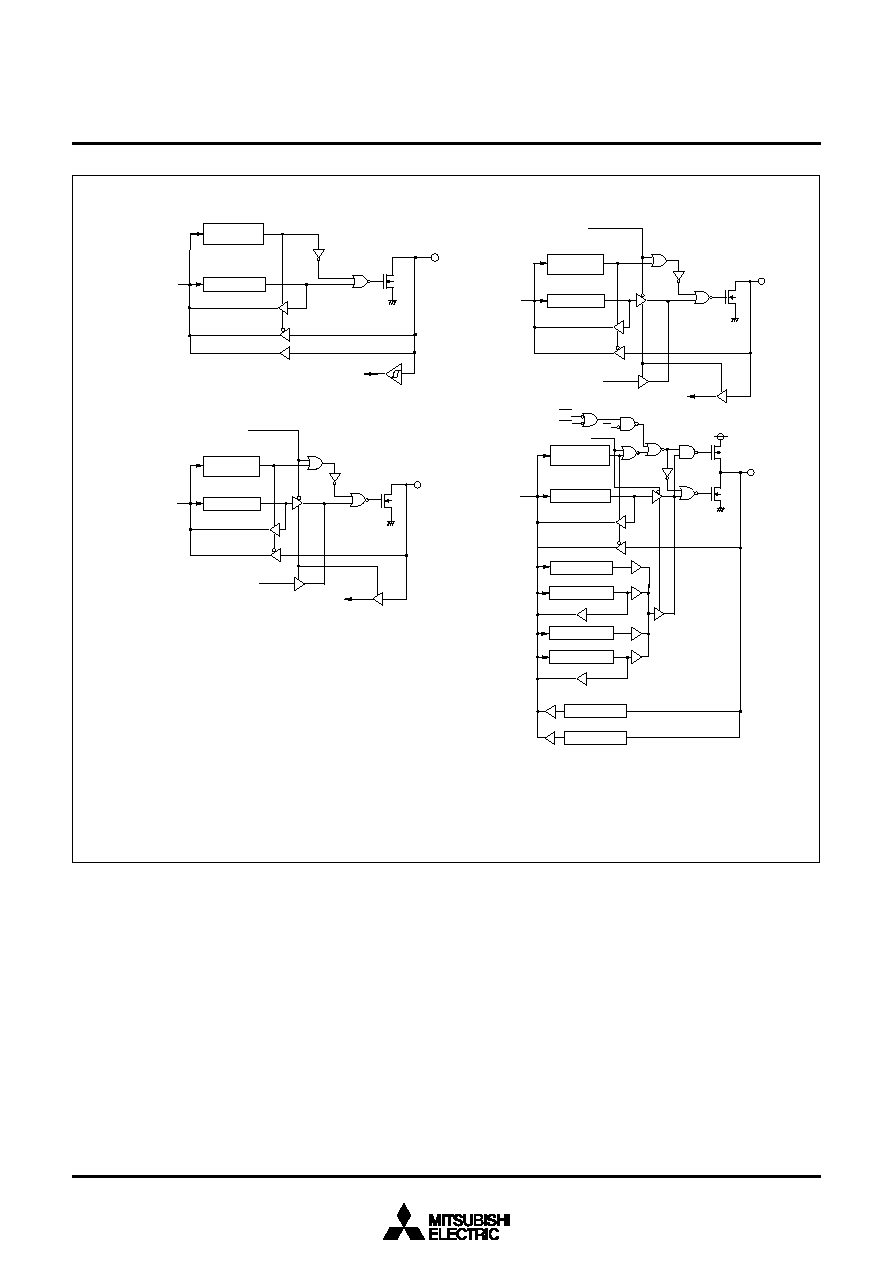
17
3886 Group
SINGLE-CHIP 8-BIT CMOS MICROCOMPUTER
MITSUBISHI MICROCOMPUTERS
Fig. 13 Port block diagram (4)
(
2
8
)
P
o
r
t
P
8
O
u
t
p
u
t
b
u
f
f
e
r
0
S
t
a
t
u
s
r
e
g
i
s
t
e
r
0
O
u
t
p
u
t
b
u
f
f
e
r
1
S
t
a
t
u
s
r
e
g
i
s
t
e
r
1
I
n
p
u
t
b
u
f
f
e
r
0
I
n
p
u
t
b
u
f
f
e
r
1
D
a
t
a
b
u
s
b
u
f
f
e
r
e
n
a
b
l
e
b
i
t
(
2
6
)
P
o
r
t
P
7
6
D
a
t
a
b
u
s
P
o
r
t
l
a
t
c
h
D
i
r
e
c
t
i
o
n
r
e
g
i
s
t
e
r
S
D
A
o
u
t
p
u
t
S
D
A
i
n
p
u
t
T
6
(
2
7
)
P
o
r
t
P
7
7
I
2
C
-
B
U
S
i
n
t
e
r
f
a
c
e
e
n
a
b
l
e
b
i
t
S
C
L
o
u
t
p
u
t
S
C
L
i
n
p
u
t
T
6
(
2
5
)
P
o
r
t
s
P
7
4
,
P
7
5
D
a
t
a
b
u
s
P
o
r
t
l
a
t
c
h
D
i
r
e
c
t
i
o
n
r
e
g
i
s
t
e
r
T
4
I
N
T
3
1
,
I
N
T
4
1
i
n
t
e
r
r
u
p
t
i
n
p
u
t
T
3
S
0
R
S
1
T
5
T
3
I
2
C
-
B
U
S
i
n
t
e
r
f
a
c
e
e
n
a
b
l
e
b
i
t
D
i
r
e
c
t
i
o
n
r
e
g
i
s
t
e
r
P
o
r
t
l
a
t
c
h
D
a
t
a
b
u
s
D
i
r
e
c
t
i
o
n
r
e
g
i
s
t
e
r
P
o
r
t
l
a
t
c
h
D
a
t
a
b
u
s
T
6
.
T
h
e
i
n
p
u
t
l
e
v
e
l
c
a
n
b
e
s
w
i
t
c
h
e
d
b
e
t
w
e
e
n
C
M
O
S
c
o
m
p
a
t
i
b
l
e
i
n
p
u
t
l
e
v
e
l
a
n
d
S
M
B
U
S
l
e
v
e
l
b
y
t
h
e
I2C
-
B
U
S
i
n
t
e
r
f
a
c
e
p
i
n
i
n
p
u
t
s
e
l
e
c
t
i
o
n
b
i
t
o
f
t
h
e
I
2
C
c
o
n
t
r
o
l
r
e
g
i
s
t
e
r
(
a
d
d
r
e
s
s
0
0
1
5
1
6
)
.
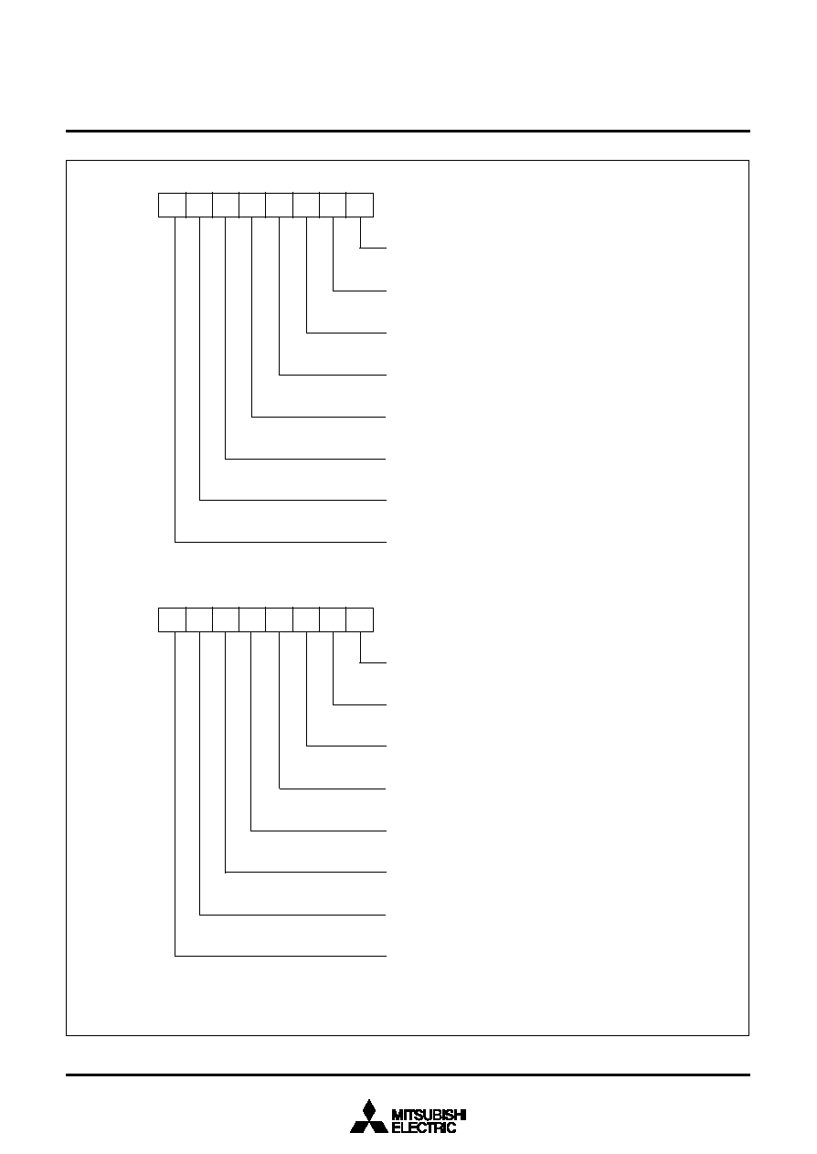
18
3886 Group
SINGLE-CHIP 8-BIT CMOS MICROCOMPUTER
MITSUBISHI MICROCOMPUTERS
Fig. 14 Structure of port I/O related register
P
o
r
t
c
o
n
t
r
o
l
r
e
g
i
s
t
e
r
1
b
7
b
0
P
o
r
t
c
o
n
t
r
o
l
r
e
g
i
s
t
e
r
2
P
0
0
≠
P
0
3
o
u
t
p
u
t
s
t
r
u
c
t
u
r
e
s
e
l
e
c
t
i
o
n
b
i
t
0
:
C
M
O
S
1
:
N
-
c
h
a
n
n
e
l
o
p
e
n
-
d
r
a
i
n
P
0
4
≠
P
0
7
o
u
t
p
u
t
s
t
r
u
c
t
u
r
e
s
e
l
e
c
t
i
o
n
b
i
t
0
:
C
M
O
S
1
:
N
-
c
h
a
n
n
e
l
o
p
e
n
-
d
r
a
i
n
P
1
0
≠
P
1
3
o
u
t
p
u
t
s
t
r
u
c
t
u
r
e
s
e
l
e
c
t
i
o
n
b
i
t
0
:
C
M
O
S
1
:
N
-
c
h
a
n
n
e
l
o
p
e
n
-
d
r
a
i
n
P
1
4
≠
P
1
7
o
u
t
p
u
t
s
t
r
u
c
t
u
r
e
s
e
l
e
c
t
i
o
n
b
i
t
0
:
C
M
O
S
1
:
N
-
c
h
a
n
n
e
l
o
p
e
n
-
d
r
a
i
n
P
3
0
≠
P
3
3
p
u
l
l
-
u
p
c
o
n
t
r
o
l
b
i
t
0
:
N
o
p
u
l
l
-
u
p
1
:
P
u
l
l
-
u
p
P
3
4
≠
P
3
7
p
u
l
l
-
u
p
c
o
n
t
r
o
l
b
i
t
0
:
N
o
p
u
l
l
-
u
p
1
:
P
u
l
l
-
u
p
P
W
M
0
e
n
a
b
l
e
b
i
t
0
:
P
W
M
0
o
u
t
p
u
t
d
i
s
a
b
l
e
d
1
:
P
W
M
0
o
u
t
p
u
t
e
n
a
b
l
e
d
P
W
M
1
e
n
a
b
l
e
b
i
t
0
:
P
W
M
1
o
u
t
p
u
t
d
i
s
a
b
l
e
d
1
:
P
W
M
1
o
u
t
p
u
t
e
n
a
b
l
e
d
P
4
i
n
p
u
t
l
e
v
e
l
s
e
l
e
c
t
i
o
n
b
i
t
(
P
4
2
≠
P
4
6
)
0
:
C
M
O
S
l
e
v
e
l
i
n
p
u
t
1
:
T
T
L
l
e
v
e
l
i
n
p
u
t
P
7
i
n
p
u
t
l
e
v
e
l
s
e
l
e
c
t
i
o
n
b
i
t
(
P
7
0
≠
P
7
5
)
0
:
C
M
O
S
l
e
v
e
l
i
n
p
u
t
1
:
T
T
L
l
e
v
e
l
i
n
p
u
t
P
4
o
u
t
p
u
t
s
t
r
u
c
t
u
r
e
s
e
l
e
c
t
i
o
n
b
i
t
(
P
4
2
,
P
4
3
,
P
4
4
,
P
4
6
)
0
:
C
M
O
S
1
:
N
-
c
h
a
n
n
e
l
o
p
e
n
-
d
r
a
i
n
P
8
f
u
n
c
t
i
o
n
s
e
l
e
c
t
i
o
n
b
i
t
0
:
P
o
r
t
P
8
/
P
o
r
t
P
8
d
i
r
e
c
t
i
o
n
r
e
g
i
s
t
e
r
1
:
P
o
r
t
P
4
i
n
p
u
t
r
e
g
i
s
t
e
r
/
P
o
r
t
P
7
i
n
p
u
t
r
e
g
i
s
t
e
r
I
N
T
2
,
I
N
T
3
,
I
N
T
4
i
n
t
e
r
r
u
p
t
s
w
i
t
c
h
b
i
t
0
:
I
N
T
2
0
,
I
N
T
3
0
,
I
N
T
4
0
i
n
t
e
r
r
u
p
t
1
:
I
N
T
2
1
,
I
N
T
3
1
,
I
N
T
4
1
i
n
t
e
r
r
u
p
t
T
i
m
e
r
Y
c
o
u
n
t
s
o
u
r
c
e
s
e
l
e
c
t
i
o
n
b
i
t
0
:
f
(
X
I
N
)
/
1
6
(
f
(
X
C
I
N
)
/
1
6
i
n
l
o
w
-
s
p
e
e
d
m
o
d
e
)
1
:
f
(
X
C
I
N
)
O
s
c
i
l
l
a
t
i
o
n
s
t
a
b
i
l
i
z
i
n
g
t
i
m
e
s
e
t
a
f
t
e
r
S
T
P
i
n
s
t
r
u
c
t
i
o
n
r
e
l
e
a
s
e
d
b
i
t
1
:
N
o
a
u
t
o
m
a
t
i
c
s
e
t
P
o
r
t
o
u
t
p
u
t
P
4
2
/
P
4
3
c
l
e
a
r
f
u
n
c
t
i
o
n
s
e
l
e
c
t
i
o
n
b
i
t
0
:
O
n
l
y
s
o
f
t
w
a
r
e
c
l
e
a
r
1
:
S
o
f
t
w
a
r
e
c
l
e
a
r
a
n
d
o
u
t
p
u
t
d
a
t
a
b
u
s
b
u
f
f
e
r
0
r
e
a
d
i
n
g
(
s
y
s
t
e
m
b
u
s
s
i
d
e
)
b
7
b
0
(
P
C
T
L
1
:
a
d
d
r
e
s
s
0
0
2
E
1
6
)
(
P
C
T
L
2
:
a
d
d
r
e
s
s
0
0
2
F
1
6
)
0
:
A
u
t
o
m
a
t
i
c
s
e
t
"
0
1
1
6
"
t
o
t
i
m
e
r
1
a
n
d
"
F
F
1
6
"
t
o
p
r
e
s
c
a
l
e
r
1
2

19
3886 Group
SINGLE-CHIP 8-BIT CMOS MICROCOMPUTER
MITSUBISHI MICROCOMPUTERS
INTERRUPTS
Interrupts occur by 16 sources among 21 sources: nine external,
eleven internal, and one software.
Interrupt Control
Each interrupt is controlled by an interrupt request bit, an interrupt
enable bit, and the interrupt disable flag except for the software in-
terrupt set by the BRK instruction. An interrupt occurs if the
corresponding interrupt request and enable bits are "1" and the in-
terrupt disable flag is "0".
Interrupt enable bits can be set or cleared by software.
Interrupt request bits can be cleared by software, but cannot be
set by software.
The BRK instruction cannot be disabled with any flag or bit. The I
(interrupt disable) flag disables all interrupts except the BRK in-
struction interrupt.
When several interrupts occur at the same time, the interrupts are
received according to priority.
Interrupt Operation
By acceptance of an interrupt, the following operations are auto-
matically performed:
1. The contents of the program counter and the processor status
register are automatically pushed onto the stack.
2. The interrupt disable flag is set and the corresponding interrupt
request bit is cleared.
3. The interrupt jump destination address is read from the vector
table into the program counter.
Interrupt Source Selection
Any of the following interrupt sources can be selected by the inter-
rupt source selection register (address 0039
16
).
1. INT
0
or Input buffer full
2. INT
1
or Output buffer empty
3. Serial I/O1 transmission or S
CL
S
DA
4. CNTR
0
or S
CL
S
DA
5. Serial I/O2 or I
2
C
6. INT
2
or I
2
C
7. CNTR
1
or Key-on wake-up
8. A-D conversion or Key-on wake-up
External Interrupt Pin Selection
The occurrence sources of the external interrupt INT
2
, INT
3
, and
INT
4
can be selected from either input from INT
20
, INT
30
, INT
40
pin, or input from INT
21
, INT
31
, INT
41
pin by the INT
2
, INT
3
, INT
4
interrupt switch bit (bit 4 of address 002F
16
).
s
Notes
When setting of the following register or bit is changed, the inter-
rupt request bit may be set to "1."
∑ Interrupt edge selection register (address 003A
16
)
∑ Interrupt source selection register (address 0039
16
)
∑ INT
2
, INT
3
, INT
4
interrupt switch bit of
P
ort control register 2 (bit
4 of address 002F
16
)
Accept the interrupt after clearing the interrupt request bit to "0"
after interrupt is disabled and the above register or bit is set.
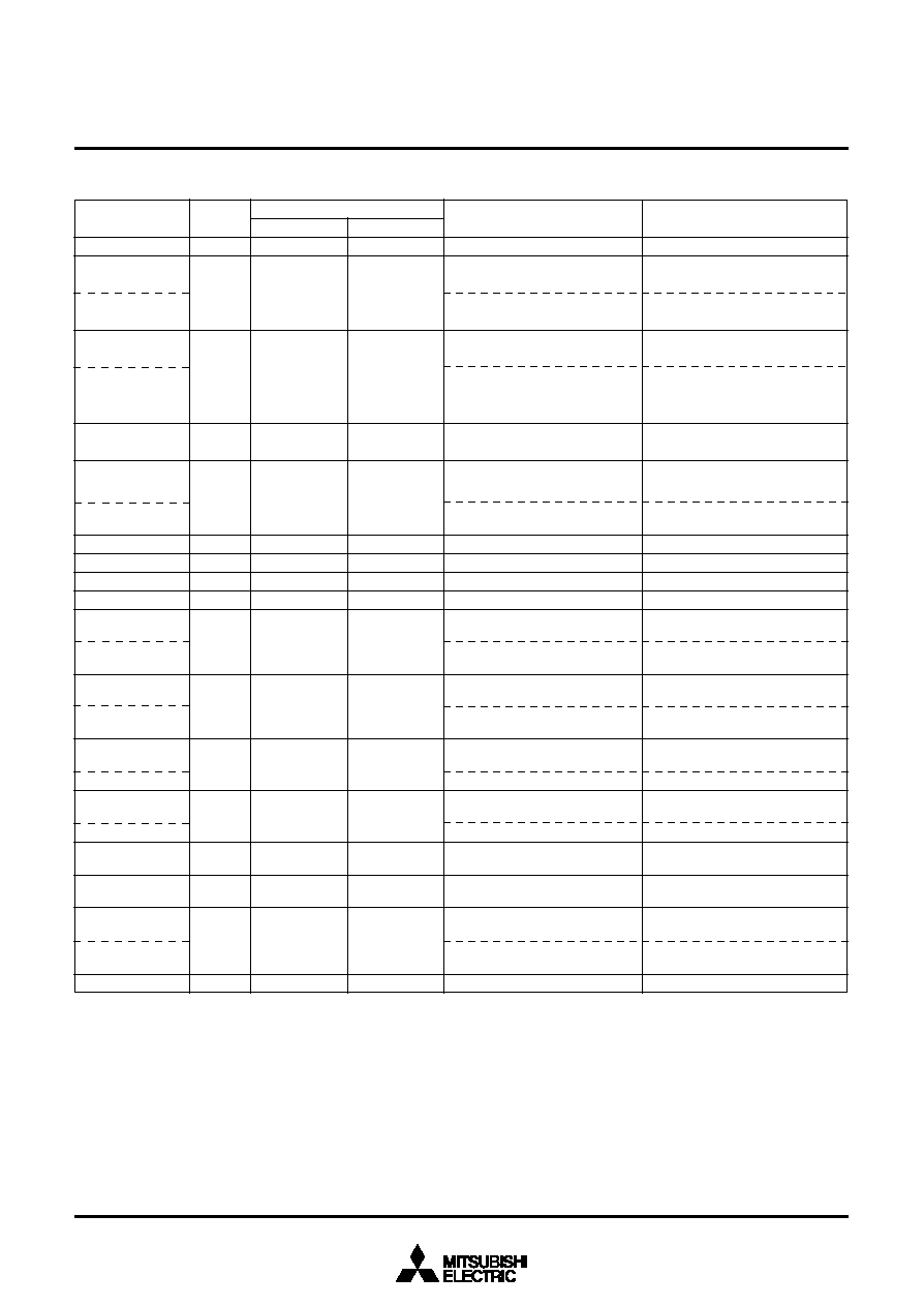
20
3886 Group
SINGLE-CHIP 8-BIT CMOS MICROCOMPUTER
MITSUBISHI MICROCOMPUTERS
Interrupt Request
Generating Conditions
Remarks
Interrupt Source
Low
FFFC
16
FFFA
16
FFF8
16
FFF6
16
FFF4
16
FFF2
16
FFF0
16
FFEE
16
FFEC
16
FFEA
16
FFE8
16
FFE6
16
FFE4
16
FFE2
16
FFE0
16
FFDE
16
FFDC
16
High
FFFD
16
FFFB
16
FFF9
16
FFF7
16
FFF5
16
FFF3
16
FFF1
16
FFEF
16
FFED
16
FFEB
16
FFE9
16
FFE7
16
FFE5
16
FFE3
16
FFE1
16
FFDF
16
FFDD
16
Priority
1
2
3
4
5
6
7
8
9
10
11
12
13
14
15
16
17
Table 6 Interrupt vector addresses and priority
Notes 1: Vector addresses contain interrupt jump destination addresses.
2: Reset function in the same way as an interrupt with the highest priority.
Vector Addresses (Note 1)
Reset (Note 2)
INT
0
Input buffer full
(IBF)
INT
1
Output buffer
empty (OBE)
Serial I/O1
reception
Serial I/O1
transmission
S
CL
, S
DA
Timer X
Timer Y
Timer 1
Timer 2
CNTR
0
S
CL
, S
DA
CNTR
1
Key-on wake-up
Serial I/O2
I
2
C
INT
2
I
2
C
INT
3
INT
4
A-D converter
Key-on wake-up
BRK instruction
At reset
At detection of either rising or
falling edge of INT
0
input
At input data bus buffer writing
At detection of either rising or
falling edge of INT
1
input
At output data bus buffer read-
ing
At completion of serial I/O1 data
reception
At completion of serial I/O1
transfer shift or when transmis-
sion buffer is empty
At detection of either rising or
falling edge of S
CL
or S
DA
At timer X underflow
At timer Y underflow
At timer 1 underflow
At timer 2 underflow
At detection of either rising or
falling edge of CNTR
0
input
At detection of either rising or
falling edge of S
CL
or S
DA
At detection of either rising or
falling edge of CNTR
1
input
At falling of port P3 (at input) in-
put logical level AND
At completion of serial I/O2 data
transfer
At completion of data transfer
At detection of either rising or
falling edge of INT
2
input
At completion of data transfer
At detection of either rising or
falling edge of INT
3
input
At detection of either rising or
falling edge of INT
4
input
At completion of A-D conversion
At falling of port P3 (at input) in-
put logical level AND
At BRK instruction execution
Non-maskable
External interrupt
(active edge selectable)
External interrupt
(active edge selectable)
Valid when serial I/O1 is selected
Valid when serial I/O1 is selected
External interrupt
(active edge selectable)
STP release timer underflow
External interrupt
(active edge selectable)
External interrupt
(active edge selectable)
External interrupt
(active edge selectable)
External interrupt (falling valid)
Valid when serial I/O2 is selected
External interrupt
(active edge selectable)
External interrupt
(active edge selectable)
External interrupt
(active edge selectable)
External interrupt (falling valid)
Non-maskable software interrupt
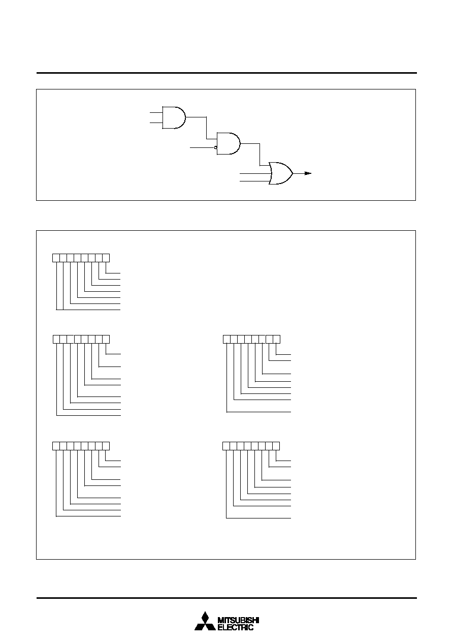
21
3886 Group
SINGLE-CHIP 8-BIT CMOS MICROCOMPUTER
MITSUBISHI MICROCOMPUTERS
Fig. 15 Interrupt control
Fig. 16 Structure of interrupt-related registers (1)
I
n
t
e
r
r
u
p
t
d
i
s
a
b
l
e
f
l
a
g
(
I
)
I
n
t
e
r
r
u
p
t
r
e
q
u
e
s
t
I
n
t
e
r
r
u
p
t
r
e
q
u
e
s
t
b
i
t
I
n
t
e
r
r
u
p
t
e
n
a
b
l
e
b
i
t
B
R
K
i
n
s
t
r
u
c
t
i
o
n
R
e
s
e
t
I
n
t
e
r
r
u
p
t
e
d
g
e
s
e
l
e
c
t
i
o
n
r
e
g
i
s
t
e
r
I
N
T
0
a
c
t
i
v
e
e
d
g
e
s
e
l
e
c
t
i
o
n
b
i
t
I
N
T
1
a
c
t
i
v
e
e
d
g
e
s
e
l
e
c
t
i
o
n
b
i
t
N
o
t
u
s
e
d
(
r
e
t
u
r
n
s
"
0
"
w
h
e
n
r
e
a
d
)
I
N
T
2
a
c
t
i
v
e
e
d
g
e
s
e
l
e
c
t
i
o
n
b
i
t
I
N
T
3
a
c
t
i
v
e
e
d
g
e
s
e
l
e
c
t
i
o
n
b
i
t
I
N
T
4
a
c
t
i
v
e
e
d
g
e
s
e
l
e
c
t
i
o
n
b
i
t
N
o
t
u
s
e
d
(
r
e
t
u
r
n
s
"
0
"
w
h
e
n
r
e
a
d
)
(
I
N
T
E
D
G
E
:
a
d
d
r
e
s
s
0
0
3
A
1
6
)
I
n
t
e
r
r
u
p
t
r
e
q
u
e
s
t
r
e
g
i
s
t
e
r
1
I
N
T
0
/
i
n
p
u
t
b
u
f
f
e
r
f
u
l
l
i
n
t
e
r
r
u
p
t
r
e
q
u
e
s
t
b
i
t
I
N
T
1
/
o
u
t
p
u
t
b
u
f
f
e
r
e
m
p
t
y
i
n
t
e
r
r
u
p
t
r
e
q
u
e
s
t
b
i
t
S
e
r
i
a
l
I
/
O
1
r
e
c
e
i
v
e
i
n
t
e
r
r
u
p
t
r
e
q
u
e
s
t
b
i
t
S
e
r
i
a
l
I
/
O
1
t
r
a
n
s
m
i
t
/
S
C
L
,
S
D
A
i
n
t
e
r
r
u
p
t
r
e
q
u
e
s
t
b
i
t
T
i
m
e
r
X
i
n
t
e
r
r
u
p
t
r
e
q
u
e
s
t
b
i
t
T
i
m
e
r
Y
i
n
t
e
r
r
u
p
t
r
e
q
u
e
s
t
b
i
t
T
i
m
e
r
1
i
n
t
e
r
r
u
p
t
r
e
q
u
e
s
t
b
i
t
T
i
m
e
r
2
i
n
t
e
r
r
u
p
t
r
e
q
u
e
s
t
b
i
t
I
n
t
e
r
r
u
p
t
c
o
n
t
r
o
l
r
e
g
i
s
t
e
r
1
I
N
T
0
/
i
n
p
u
t
b
u
f
f
e
r
f
u
l
l
i
n
t
e
r
r
u
p
t
e
n
a
b
l
e
b
i
t
I
N
T
1
/
o
u
t
p
u
t
b
u
f
f
e
r
e
m
p
t
y
i
n
t
e
r
r
u
p
t
e
n
a
b
l
e
b
i
t
S
e
r
i
a
l
I
/
O
1
r
e
c
e
i
v
e
i
n
t
e
r
r
u
p
t
e
n
a
b
l
e
b
i
t
S
e
r
i
a
l
I
/
O
1
t
r
a
n
s
m
i
t
/
S
C
L
,
S
D
A
i
n
t
e
r
r
u
p
t
e
n
a
b
l
e
b
i
t
T
i
m
e
r
X
i
n
t
e
r
r
u
p
t
e
n
a
b
l
e
b
i
t
T
i
m
e
r
Y
i
n
t
e
r
r
u
p
t
e
n
a
b
l
e
b
i
t
T
i
m
e
r
1
i
n
t
e
r
r
u
p
t
e
n
a
b
l
e
b
i
t
T
i
m
e
r
2
i
n
t
e
r
r
u
p
t
e
n
a
b
l
e
b
i
t
0
:
N
o
i
n
t
e
r
r
u
p
t
r
e
q
u
e
s
t
i
s
s
u
e
d
1
:
I
n
t
e
r
r
u
p
t
r
e
q
u
e
s
t
i
s
s
u
e
d
(
I
R
E
Q
1
:
a
d
d
r
e
s
s
0
0
3
C
1
6
)
(
I
C
O
N
1
:
a
d
d
r
e
s
s
0
0
3
E
1
6
)
I
n
t
e
r
r
u
p
t
r
e
q
u
e
s
t
r
e
g
i
s
t
e
r
2
C
N
T
R
0
/
S
C
L
,
S
D
A
i
n
t
e
r
r
u
p
t
r
e
q
u
e
s
t
b
i
t
C
N
T
R
1
/
k
e
y
-
o
n
w
a
k
e
-
u
p
i
n
t
e
r
r
u
p
t
r
e
q
u
e
s
t
b
i
t
S
e
r
i
a
l
I
/
O
2
/
I
2
C
i
n
t
e
r
r
u
p
t
r
e
q
u
e
s
t
b
i
t
I
N
T
2
/
I
2
C
i
n
t
e
r
r
u
p
t
r
e
q
u
e
s
t
b
i
t
I
N
T
3
i
n
t
e
r
r
u
p
t
r
e
q
u
e
s
t
b
i
t
I
N
T
4
i
n
t
e
r
r
u
p
t
r
e
q
u
e
s
t
b
i
t
A
D
c
o
n
v
e
r
t
e
r
/
k
e
y
-
o
n
w
a
k
e
-
u
p
i
n
t
e
r
r
u
p
t
r
e
q
u
e
s
t
b
i
t
N
o
t
u
s
e
d
(
r
e
t
u
r
n
s
"
0
"
w
h
e
n
r
e
a
d
)
(
I
R
E
Q
2
:
a
d
d
r
e
s
s
0
0
3
D
1
6
)
I
n
t
e
r
r
u
p
t
c
o
n
t
r
o
l
r
e
g
i
s
t
e
r
2
C
N
T
R
0
/
S
C
L
,
S
D
A
i
n
t
e
r
r
u
p
t
e
n
a
b
l
e
b
i
t
C
N
T
R
1
/
k
e
y
-
o
n
w
a
k
e
-
u
p
i
n
t
e
r
r
u
p
t
e
n
a
b
l
e
b
i
t
S
e
r
i
a
l
I
/
O
2
/
I
2
C
i
n
t
e
r
r
u
p
t
e
n
a
b
l
e
b
i
t
I
N
T
2
/
I
2
C
i
n
t
e
r
r
u
p
t
e
n
a
b
l
e
b
i
t
I
N
T
3
i
n
t
e
r
r
u
p
t
e
n
a
b
l
e
b
i
t
I
N
T
4
i
n
t
e
r
r
u
p
t
e
n
a
b
l
e
b
i
t
A
D
c
o
n
v
e
r
t
e
r
/
k
e
y
-
o
n
w
a
k
e
-
u
p
i
n
t
e
r
r
u
p
t
e
n
a
b
l
e
b
i
t
N
o
t
u
s
e
d
(
r
e
t
u
r
n
s
"
0
"
w
h
e
n
r
e
a
d
)
(
D
o
n
o
t
w
r
i
t
e
"
1
"
t
o
t
h
i
s
b
i
t
)
0
:
I
n
t
e
r
r
u
p
t
s
d
i
s
a
b
l
e
d
1
:
I
n
t
e
r
r
u
p
t
s
e
n
a
b
l
e
d
(
I
C
O
N
2
:
a
d
d
r
e
s
s
0
0
3
F
1
6
)
0
:
F
a
l
l
i
n
g
e
d
g
e
a
c
t
i
v
e
1
:
R
i
s
i
n
g
e
d
g
e
a
c
t
i
v
e
b
7
b
0
b
7
b
0
b
7
b
0
b
7
b
0
b
7
b
0
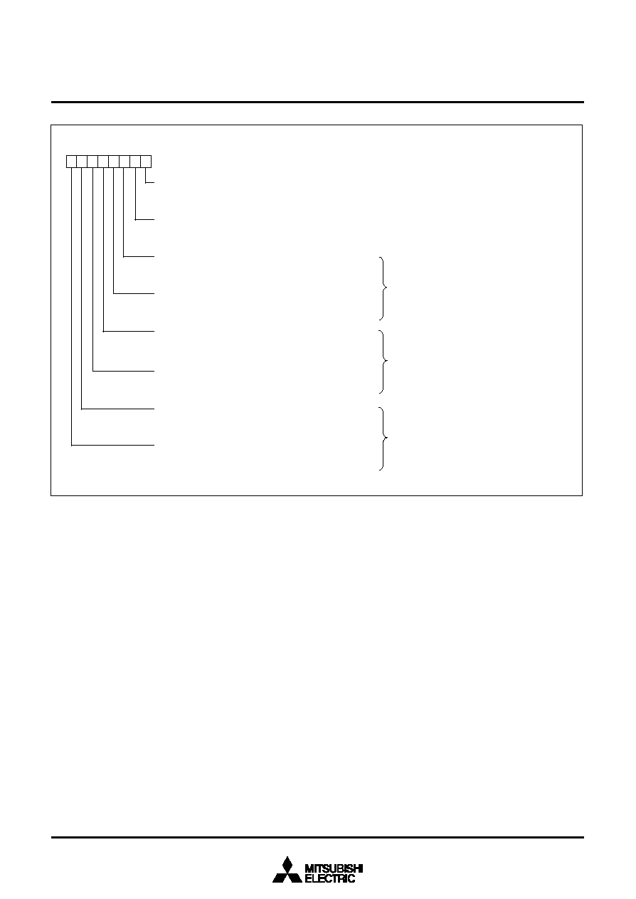
22
3886 Group
SINGLE-CHIP 8-BIT CMOS MICROCOMPUTER
MITSUBISHI MICROCOMPUTERS
Fig. 17 Structure of interrupt-related registers (2)
b
7
b
0
I
N
T
0
/
i
n
p
u
t
b
u
f
f
e
r
f
u
l
l
i
n
t
e
r
r
u
p
t
s
o
u
r
c
e
s
e
l
e
c
t
i
o
n
b
i
t
0
:
I
N
T
0
i
n
t
e
r
r
u
p
t
1
:
I
n
p
u
t
b
u
f
f
e
r
f
u
l
l
i
n
t
e
r
r
u
p
t
I
N
T
1
/
o
u
t
p
u
t
b
u
f
f
e
r
e
m
p
t
y
i
n
t
e
r
r
u
p
t
s
o
u
r
c
e
s
e
l
e
c
t
i
o
n
b
i
t
0
:
I
N
T
1
i
n
t
e
r
r
u
p
t
1
:
O
u
t
p
u
t
b
u
f
f
e
r
e
m
p
t
y
i
n
t
e
r
r
u
p
t
S
e
r
i
a
l
I
/
O
1
t
r
a
n
s
m
i
t
/
S
C
L
,
S
D
A
i
n
t
e
r
r
u
p
t
s
o
u
r
c
e
s
e
l
e
c
t
i
o
n
b
i
t
0
:
S
e
r
i
a
l
I
/
O
1
t
r
a
n
s
m
i
t
i
n
t
e
r
r
u
p
t
1
:
S
C
L
,
S
D
A
i
n
t
e
r
r
u
p
t
C
N
T
R
0
/
S
C
L
,
S
D
A
i
n
t
e
r
r
u
p
t
s
o
u
r
c
e
s
e
l
e
c
t
i
o
n
b
i
t
0
:
C
N
T
R
0
i
n
t
e
r
r
u
p
t
1
:
S
C
L
,
S
D
A
i
n
t
e
r
r
u
p
t
S
e
r
i
a
l
I
/
O
2
/
I
2
C
i
n
t
e
r
r
u
p
t
s
o
u
r
c
e
s
e
l
e
c
t
i
o
n
b
i
t
0
:
S
e
r
i
a
l
I
/
O
2
i
n
t
e
r
r
u
p
t
1
:
I
2
C
i
n
t
e
r
r
u
p
t
I
N
T
2
/
I
2
C
i
n
t
e
r
r
u
p
t
s
o
u
r
c
e
s
e
l
e
c
t
i
o
n
b
i
t
0
:
I
N
T
2
i
n
t
e
r
r
u
p
t
1
:
I
2
C
i
n
t
e
r
r
u
p
t
C
N
T
R
1
/
k
e
y
-
o
n
w
a
k
e
-
u
p
i
n
t
e
r
r
u
p
t
s
o
u
r
c
e
s
e
l
e
c
t
i
o
n
b
i
t
0
:
C
N
T
R
1
i
n
t
e
r
r
u
p
t
1
:
K
e
y
-
o
n
w
a
k
e
-
u
p
i
n
t
e
r
r
u
p
t
A
D
c
o
n
v
e
r
t
e
r
/
k
e
y
-
o
n
w
a
k
e
-
u
p
i
n
t
e
r
r
u
p
t
s
o
u
r
c
e
s
e
l
e
c
t
i
o
n
b
i
t
0
:
A
-
D
c
o
n
v
e
r
t
e
r
i
n
t
e
r
r
u
p
t
1
:
K
e
y
-
o
n
w
a
k
e
-
u
p
i
n
t
e
r
r
u
p
t
I
n
t
e
r
r
u
p
t
s
o
u
r
c
e
s
e
l
e
c
t
i
o
n
r
e
g
i
s
t
e
r
(
D
o
n
o
t
w
r
i
t
e
"
1
"
t
o
t
h
e
s
e
b
i
t
s
s
i
m
u
l
t
a
n
e
o
u
s
l
y
.
)
(
D
o
n
o
t
w
r
i
t
e
"
1
"
t
o
t
h
e
s
e
b
i
t
s
s
i
m
u
l
t
a
n
e
o
u
s
l
y
.
)
(
D
o
n
o
t
w
r
i
t
e
"
1
"
t
o
t
h
e
s
e
b
i
t
s
s
i
m
u
l
t
a
n
e
o
u
s
l
y
.
)
(
I
N
T
S
E
L
:
a
d
d
r
e
s
s
0
0
3
9
1
6
)
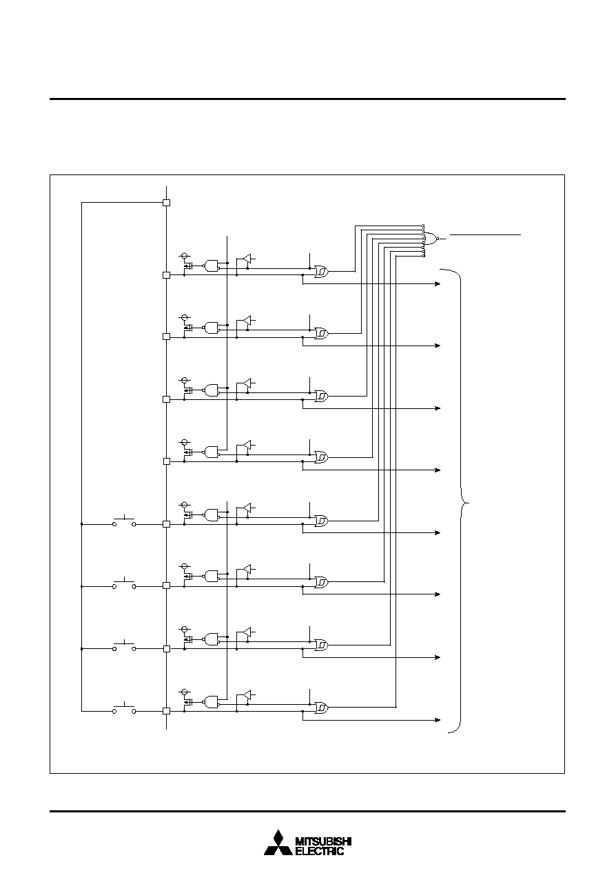
23
3886 Group
SINGLE-CHIP 8-BIT CMOS MICROCOMPUTER
MITSUBISHI MICROCOMPUTERS
Key Input Interrupt (Key-on Wake Up)
A Key input interrupt request is generated by applying "L" level to
any pin of port P3 that have been set to input mode. In other
words, it is generated when AND of input level goes from "1" to
"0". An example of using a key input interrupt is shown in Figure
18, where an interrupt request is generated by pressing one of the
keys consisted as an active-low key matrix which inputs to ports
P3
0
≠P3
3
.
Fig. 18 Connection example when using key input interrupt and port P3 block diagram
T
T
T
T
T
T
T
T
T
T
T
T
T
T
T
T
T
T
T
T
T
T
T
T
P
o
r
t
P
3
0
l
a
t
c
h
P
o
r
t
P
3
0
d
i
r
e
c
t
i
o
n
r
e
g
i
s
t
e
r
=
"
0
"
P
o
r
t
P
3
1
l
a
t
c
h
P
o
r
t
P
3
1
d
i
r
e
c
t
i
o
n
r
e
g
i
s
t
e
r
=
"
0
"
P
o
r
t
P
3
2
l
a
t
c
h
P
o
r
t
P
3
2
d
i
r
e
c
t
i
o
n
r
e
g
i
s
t
e
r
=
"
0
"
P
o
r
t
P
3
3
l
a
t
c
h
P
o
r
t
P
3
3
d
i
r
e
c
t
i
o
n
r
e
g
i
s
t
e
r
=
"
0
"
P
o
r
t
P
3
4
l
a
t
c
h
P
o
r
t
P
3
4
d
i
r
e
c
t
i
o
n
r
e
g
i
s
t
e
r
=
"
1
"
P
o
r
t
P
3
5
l
a
t
c
h
P
o
r
t
P
3
5
d
i
r
e
c
t
i
o
n
r
e
g
i
s
t
e
r
=
"
1
"
P
o
r
t
P
3
6
l
a
t
c
h
P
o
r
t
P
3
6
d
i
r
e
c
t
i
o
n
r
e
g
i
s
t
e
r
=
"
1
"
P
o
r
t
P
3
7
l
a
t
c
h
P
o
r
t
P
3
7
d
i
r
e
c
t
i
o
n
r
e
g
i
s
t
e
r
=
"
1
"
P
3
0
i
n
p
u
t
P
3
1
i
n
p
u
t
P
3
2
i
n
p
u
t
P
3
3
i
n
p
u
t
P
3
4
o
u
t
p
u
t
P
3
5
o
u
t
p
u
t
P
3
6
o
u
t
p
u
t
P
3
7
o
u
t
p
u
t
P
o
r
t
c
o
n
t
r
o
l
r
e
g
i
s
t
e
r
1
B
i
t
5
=
"
1
"
P
o
r
t
P
3
I
n
p
u
t
r
e
a
d
i
n
g
c
i
r
c
u
i
t
C
o
m
p
a
r
a
t
o
r
c
i
r
c
u
i
t
P
o
r
t
P
X
x
"
L
"
l
e
v
e
l
o
u
t
p
u
t
T
P
-
c
h
a
n
n
e
l
t
r
a
n
s
i
s
t
o
r
f
o
r
p
u
l
l
-
u
p
T
T
C
M
O
S
o
u
t
p
u
t
b
u
f
f
e
r
K
e
y
i
n
p
u
t
i
n
t
e
r
r
u
p
t
r
e
q
u
e
s
t
P
o
r
t
c
o
n
t
r
o
l
r
e
g
i
s
t
e
r
1
B
i
t
4
=
"
1
"
24
3886 Group
SINGLE-CHIP 8-BIT CMOS MICROCOMPUTER
MITSUBISHI MICROCOMPUTERS
TIMERS
The 3886 group has four timers: timer X, timer Y, timer 1, and
timer 2.
The division ratio of each timer or prescaler is given by 1/(n + 1),
where n is the value in the corresponding timer or prescaler latch.
All timers are count down. When the timer reaches "00
16
", an un-
derflow occurs at the next count pulse and the corresponding
timer latch is reloaded into the timer and the count is continued.
When a timer underflows, the interrupt request bit corresponding
to that timer is set to "1".
Timer 1 and Timer 2
The count source of prescaler 12 is the oscillation frequency di-
vided by 16. The output of prescaler 12 is counted by timer 1 and
timer 2, and a timer underflow sets the interrupt request bit.
Timer X and Timer Y
Timer X and Timer Y can each select in one of four operating
modes by setting the timer XY mode register.
(1) Timer Mode
The timer counts f(X
IN
)/16.
(2) Pulse Output Mode
Timer X (or timer Y) counts f(X
IN
)/16. Whenever the contents of
the timer reach "00
16
", the signal output from the CNTR
0
(or
CNTR
1
) pin is inverted. If the CNTR
0
(or CNTR
1
) active edge se-
lection bit is "0", output begins at " H".
If it is "1", output starts at "L". When using a timer in this mode, set
the corresponding port P5
4
( or port P5
5
) direction register to out-
put mode.
(3) Event Counter Mode
Operation in event counter mode is the same as in timer mode,
except that the timer counts signals input through the CNTR
0
or
CNTR
1
pin.
When the CNTR
0
(or CNTR
1
) active edge selection bit is "0", the
rising edge of the CNTR
0
(or CNTR
1
) pin is counted.
When the CNTR
0
(or CNTR
1
) active edge selection bit is "1", the
falling edge of the CNTR
0
(or CNTR
1
) pin is counted.
(4) Pulse Width Measurement Mode
If the CNTR
0
(or CNTR
1
) active edge selection bit is "0", the timer
counts f(X
IN
)/16 while the CNTR
0
(or CNTR
1
) pin is at "H". If the
CNTR
0
(or CNTR
1
) active edge selection bit is "1", the timer
counts while the CNTR
0
(or CNTR
1
) pin is at "L".
The count can be stopped by setting "1" to the timer X (or timer Y)
count stop bit in any mode. The corresponding interrupt request
bit is set each time a timer overflows.
The count source for timer Y in the timer mode or the pulse output
mode can be selected from either f(X
IN
)/16 or f(X
CIN
) by the timer
Y count source selection bit of the port control register 2 (bit 5 of
address 002F
16
).
Fig. 19 Structure of timer XY mode register
T
i
m
e
r
X
c
o
u
n
t
s
t
o
p
b
i
t
0
:
C
o
u
n
t
s
t
a
r
t
1
:
C
o
u
n
t
s
t
o
p
T
i
m
e
r
X
Y
m
o
d
e
r
e
g
i
s
t
e
r
(
T
M
:
a
d
d
r
e
s
s
0
0
2
3
1
6
)
T
i
m
e
r
Y
o
p
e
r
a
t
i
n
g
m
o
d
e
b
i
t
0
0
:
T
i
m
e
r
m
o
d
e
0
1
:
P
u
l
s
e
o
u
t
p
u
t
m
o
d
e
1
0
:
E
v
e
n
t
c
o
u
n
t
e
r
m
o
d
e
1
1
:
P
u
l
s
e
w
i
d
t
h
m
e
a
s
u
r
e
m
e
n
t
m
o
d
e
C
N
T
R
1
a
c
t
i
v
e
e
d
g
e
s
e
l
e
c
t
i
o
n
b
i
t
0
:
I
n
t
e
r
r
u
p
t
a
t
f
a
l
l
i
n
g
e
d
g
e
C
o
u
n
t
a
t
r
i
s
i
n
g
e
d
g
e
i
n
e
v
e
n
t
c
o
u
n
t
e
r
m
o
d
e
1
:
I
n
t
e
r
r
u
p
t
a
t
r
i
s
i
n
g
e
d
g
e
C
o
u
n
t
a
t
f
a
l
l
i
n
g
e
d
g
e
i
n
e
v
e
n
t
c
o
u
n
t
e
r
m
o
d
e
b
7
C
N
T
R
0
a
c
t
i
v
e
e
d
g
e
s
e
l
e
c
t
i
o
n
b
i
t
0
:
I
n
t
e
r
r
u
p
t
a
t
f
a
l
l
i
n
g
e
d
g
e
C
o
u
n
t
a
t
r
i
s
i
n
g
e
d
g
e
i
n
e
v
e
n
t
c
o
u
n
t
e
r
m
o
d
e
1
:
I
n
t
e
r
r
u
p
t
a
t
r
i
s
i
n
g
e
d
g
e
C
o
u
n
t
a
t
f
a
l
l
i
n
g
e
d
g
e
i
n
e
v
e
n
t
c
o
u
n
t
e
r
m
o
d
e
b
0
T
i
m
e
r
X
o
p
e
r
a
t
i
n
g
m
o
d
e
b
i
t
0
0
:
T
i
m
e
r
m
o
d
e
0
1
:
P
u
l
s
e
o
u
t
p
u
t
m
o
d
e
1
0
:
E
v
e
n
t
c
o
u
n
t
e
r
m
o
d
e
1
1
:
P
u
l
s
e
w
i
d
t
h
m
e
a
s
u
r
e
m
e
n
t
m
o
d
e
b
1
b
0
b
5
b
4
T
i
m
e
r
Y
c
o
u
n
t
s
t
o
p
b
i
t
0
:
C
o
u
n
t
s
t
a
r
t
1
:
C
o
u
n
t
s
t
o
p

25
3886 Group
SINGLE-CHIP 8-BIT CMOS MICROCOMPUTER
MITSUBISHI MICROCOMPUTERS
Fig. 20 Block diagram of timer X, timer Y, timer 1, and timer 2
Q
Q
"
1
"
"
0
"
P
5
4
/
C
N
T
R
0
Q
Q
P
5
5
/
C
N
T
R
1
1
/
1
6
f
(
X
I
N
)
"
0
"
"
1
"
R
R
"
1
"
"
0
"
"
0
"
"
1
"
T
T
P
r
e
s
c
a
l
e
r
X
l
a
t
c
h
(
8
)
P
r
e
s
c
a
l
e
r
X
(
8
)
T
i
m
e
r
X
l
a
t
c
h
(
8
)
T
i
m
e
r
X
(
8
)
T
o
t
i
m
e
r
X
i
n
t
e
r
r
u
p
t
r
e
q
u
e
s
t
b
i
t
T
o
g
g
l
e
f
l
i
p
-
f
l
o
p
T
i
m
e
r
X
c
o
u
n
t
s
t
o
p
b
i
t
P
u
l
s
e
w
i
d
t
h
m
e
a
s
u
r
e
m
e
n
t
m
o
d
e
E
v
e
n
t
c
o
u
n
t
e
r
m
o
d
e
T
o
C
N
T
R
0
i
n
t
e
r
r
u
p
t
r
e
q
u
e
s
t
b
i
t
P
u
l
s
e
o
u
t
p
u
t
m
o
d
e
P
o
r
t
P
5
4
l
a
t
c
h
P
o
r
t
P
5
4
d
i
r
e
c
t
i
o
n
r
e
g
i
s
t
e
r
C
N
T
R
0
a
c
t
i
v
e
e
d
g
e
s
e
l
e
c
t
i
o
n
b
i
t
T
i
m
e
r
X
l
a
t
c
h
w
r
i
t
e
p
u
l
s
e
P
u
l
s
e
o
u
t
p
u
t
m
o
d
e
T
i
m
e
r
m
o
d
e
P
u
l
s
e
o
u
t
p
u
t
m
o
d
e
P
r
e
s
c
a
l
e
r
Y
l
a
t
c
h
(
8
)
P
r
e
s
c
a
l
e
r
Y
(
8
)
T
i
m
e
r
Y
l
a
t
c
h
(
8
)
T
i
m
e
r
Y
(
8
)
T
o
t
i
m
e
r
Y
i
n
t
e
r
r
u
p
t
r
e
q
u
e
s
t
b
i
t
T
o
g
g
l
e
f
l
i
p
-
f
l
o
p
T
i
m
e
r
Y
c
o
u
n
t
s
t
o
p
b
i
t
T
o
C
N
T
R
1
i
n
t
e
r
r
u
p
t
r
e
q
u
e
s
t
b
i
t
P
u
l
s
e
o
u
t
p
u
t
m
o
d
e
P
o
r
t
P
5
5
l
a
t
c
h
P
o
r
t
P
5
5
d
i
r
e
c
t
i
o
n
r
e
g
i
s
t
e
r
C
N
T
R
1
a
c
t
i
v
e
e
d
g
e
s
e
l
e
c
t
i
o
n
b
i
t
T
i
m
e
r
Y
l
a
t
c
h
w
r
i
t
e
p
u
l
s
e
P
u
l
s
e
o
u
t
p
u
t
m
o
d
e
T
i
m
e
r
m
o
d
e
P
u
l
s
e
o
u
t
p
u
t
m
o
d
e
D
a
t
a
b
u
s
D
a
t
a
b
u
s
D
i
v
i
d
e
r
O
s
c
i
l
l
a
t
o
r
P
r
e
s
c
a
l
e
r
1
2
l
a
t
c
h
(
8
)
P
r
e
s
c
a
l
e
r
1
2
(
8
)
T
i
m
e
r
1
l
a
t
c
h
(
8
)
T
i
m
e
r
1
(
8
)
D
a
t
a
b
u
s
T
i
m
e
r
2
l
a
t
c
h
(
8
)
T
i
m
e
r
2
(
8
)
T
o
t
i
m
e
r
2
i
n
t
e
r
r
u
p
t
r
e
q
u
e
s
t
b
i
t
T
o
t
i
m
e
r
1
i
n
t
e
r
r
u
p
t
r
e
q
u
e
s
t
b
i
t
C
N
T
R
0
a
c
t
i
v
e
e
d
g
e
s
e
l
e
c
t
i
o
n
b
i
t
C
N
T
R
1
a
c
t
i
v
e
e
d
g
e
s
e
l
e
c
t
i
o
n
b
i
t
P
u
l
s
e
w
i
d
t
h
m
e
a
s
u
r
e
-
m
e
n
t
m
o
d
e
E
v
e
n
t
c
o
u
n
t
e
r
m
o
d
e
1
/
1
6
f
(
X
I
N
)
D
i
v
i
d
e
r
O
s
c
i
l
l
a
t
o
r
1
/
1
6
f
(
X
I
N
)
D
i
v
i
d
e
r
O
s
c
i
l
l
a
t
o
r
f
(
X
C
I
N
)
O
s
c
i
l
l
a
t
o
r
"
0
"
"
1
"
T
i
m
e
r
Y
c
o
u
n
t
s
o
u
r
c
e
s
e
l
e
c
t
i
o
n
b
i
t
(
f
(
X
C
I
N
)
i
n
l
o
w
-
s
p
e
e
d
m
o
d
e
)
(
f
(
X
C
I
N
)
i
n
l
o
w
-
s
p
e
e
d
m
o
d
e
)
(
f
(
X
C
I
N
)
i
n
l
o
w
-
s
p
e
e
d
m
o
d
e
)
26
3886 Group
SINGLE-CHIP 8-BIT CMOS MICROCOMPUTER
MITSUBISHI MICROCOMPUTERS
SERIAL I/O
Serial I/O1
Serial I/O1 can be used as either clock synchronous or asynchro-
nous (UART) serial I/O. A dedicated timer is also provided for
baud rate generation.
(1) Clock Synchronous Serial I/O Mode
Clock synchronous serial I/O1 mode can be selected by setting
the serial I/O1 mode selection bit of the serial I/O1 control register
(bit 6 of address 001A
16
) to "1".
For clock synchronous serial I/O, the transmitter and the receiver
must use the same clock. If an internal clock is used, transfer is
started by a write signal to the TB/RB.
Fig. 21 Block diagram of clock synchronous serial I/O1
Fig. 22 Operation of clock synchronous serial I/O1 function
1
/
4
1
/
4
F
/
F
P
4
6
/
S
C
L
K
1
/
O
B
F
1
0
S
e
r
i
a
l
I
/
O
1
s
t
a
t
u
s
r
e
g
i
s
t
e
r
S
e
r
i
a
l
I
/
O
1
c
o
n
t
r
o
l
r
e
g
i
s
t
e
r
P
4
7
/
S
R
D
Y
1
/
S
1
P
4
4
/
R
X
D
P
4
5
/
T
X
D
f
(
X
I
N
)
R
e
c
e
i
v
e
b
u
f
f
e
r
r
e
g
i
s
t
e
r
A
d
d
r
e
s
s
0
0
1
8
1
6
R
e
c
e
i
v
e
s
h
i
f
t
r
e
g
i
s
t
e
r
R
e
c
e
i
v
e
b
u
f
f
e
r
f
u
l
l
f
l
a
g
(
R
B
F
)
R
e
c
e
i
v
e
i
n
t
e
r
r
u
p
t
r
e
q
u
e
s
t
(
R
I
)
C
l
o
c
k
c
o
n
t
r
o
l
c
i
r
c
u
i
t
S
h
i
f
t
c
l
o
c
k
S
e
r
i
a
l
I
/
O
1
s
y
n
c
h
r
o
n
o
u
s
c
l
o
c
k
s
e
l
e
c
t
i
o
n
b
i
t
F
r
e
q
u
e
n
c
y
d
i
v
i
s
i
o
n
r
a
t
i
o
1
/
(
n
+
1
)
B
a
u
d
r
a
t
e
g
e
n
e
r
a
t
o
r
A
d
d
r
e
s
s
0
0
1
C
1
6
B
R
G
c
o
u
n
t
s
o
u
r
c
e
s
e
l
e
c
t
i
o
n
b
i
t
C
l
o
c
k
c
o
n
t
r
o
l
c
i
r
c
u
i
t
F
a
l
l
i
n
g
-
e
d
g
e
d
e
t
e
c
t
o
r
T
r
a
n
s
m
i
t
b
u
f
f
e
r
r
e
g
i
s
t
e
r
D
a
t
a
b
u
s
A
d
d
r
e
s
s
0
0
1
8
1
6
S
h
i
f
t
c
l
o
c
k
T
r
a
n
s
m
i
t
s
h
i
f
t
c
o
m
p
l
e
t
i
o
n
f
l
a
g
(
T
S
C
)
T
r
a
n
s
m
i
t
b
u
f
f
e
r
e
m
p
t
y
f
l
a
g
(
T
B
E
)
T
r
a
n
s
m
i
t
i
n
t
e
r
r
u
p
t
r
e
q
u
e
s
t
(
T
I
)
T
r
a
n
s
m
i
t
i
n
t
e
r
r
u
p
t
s
o
u
r
c
e
s
e
l
e
c
t
i
o
n
b
i
t
A
d
d
r
e
s
s
0
0
1
9
1
6
D
a
t
a
b
u
s
A
d
d
r
e
s
s
0
0
1
A
1
6
T
r
a
n
s
m
i
t
s
h
i
f
t
r
e
g
i
s
t
e
r
(
f
(
X
C
I
N
)
i
n
l
o
w
-
s
p
e
e
d
m
o
d
e
)
D
7
D
7
D
0
D
1
D
2
D
3
D
4
D
5
D
6
D
0
D
1
D
2
D
3
D
4
D
5
D
6
R
B
F
=
1
T
S
C
=
1
T
B
E
=
0
T
B
E
=
1
T
S
C
=
0
T
r
a
n
s
f
e
r
s
h
i
f
t
c
l
o
c
k
(
1
/
2
t
o
1
/
2
0
4
8
o
f
t
h
e
i
n
t
e
r
n
a
l
c
l
o
c
k
,
o
r
a
n
e
x
t
e
r
n
a
l
c
l
o
c
k
)
S
e
r
i
a
l
o
u
t
p
u
t
T
x
D
S
e
r
i
a
l
i
n
p
u
t
R
x
D
W
r
i
t
e
p
u
l
s
e
t
o
r
e
c
e
i
v
e
/
t
r
a
n
s
m
i
t
b
u
f
f
e
r
r
e
g
i
s
t
e
r
(
a
d
d
r
e
s
s
0
0
1
8
1
6
)
O
v
e
r
r
u
n
e
r
r
o
r
(
O
E
)
d
e
t
e
c
t
i
o
n
N
o
t
e
s 1
:
A
s
t
h
e
t
r
a
n
s
m
i
t
i
n
t
e
r
r
u
p
t
(
T
I
)
,
w
h
i
c
h
c
a
n
b
e
s
e
l
e
c
t
e
d
,
e
i
t
h
e
r
w
h
e
n
t
h
e
t
r
a
n
s
m
i
t
b
u
f
f
e
r
h
a
s
e
m
p
t
i
e
d
(
T
B
E
=
1
)
o
r
a
f
t
e
r
t
h
e
t
r
a
n
s
m
i
t
s
h
i
f
t
o
p
e
r
a
t
i
o
n
h
a
s
e
n
d
e
d
(
T
S
C
=
1
)
,
b
y
s
e
t
t
i
n
g
t
h
e
t
r
a
n
s
m
i
t
i
n
t
e
r
r
u
p
t
s
o
u
r
c
e
s
e
l
e
c
t
i
o
n
b
i
t
(
T
I
C
)
o
f
t
h
e
s
e
r
i
a
l
I
/
O
1
c
o
n
t
r
o
l
r
e
g
i
s
t
e
r
.
2
:
I
f
d
a
t
a
i
s
w
r
i
t
t
e
n
t
o
t
h
e
t
r
a
n
s
m
i
t
b
u
f
f
e
r
r
e
g
i
s
t
e
r
w
h
e
n
T
S
C
=
0
,
t
h
e
t
r
a
n
s
m
i
t
c
l
o
c
k
i
s
g
e
n
e
r
a
t
e
d
c
o
n
t
i
n
u
o
u
s
l
y
a
n
d
s
e
r
i
a
l
d
a
t
a
i
s
o
u
t
p
u
t
c
o
n
t
i
n
u
o
u
s
l
y
f
r
o
m
t
h
e
T
x
D
p
i
n
.
3
:
T
h
e
r
e
c
e
i
v
e
i
n
t
e
r
r
u
p
t
(
R
I
)
i
s
s
e
t
w
h
e
n
t
h
e
r
e
c
e
i
v
e
b
u
f
f
e
r
f
u
l
l
f
l
a
g
(
R
B
F
)
b
e
c
o
m
e
s
"
1
"
.
R
e
c
e
i
v
e
e
n
a
b
l
e
s
i
g
n
a
l
S
R
D
Y
1
27
3886 Group
SINGLE-CHIP 8-BIT CMOS MICROCOMPUTER
MITSUBISHI MICROCOMPUTERS
(2) Asynchronous Serial I/O (UART) Mode
Clock asynchronous serial I/O mode (UART) can be selected by
clearing the serial I/O1 mode selection bit of the serial I/O1 control
register to "0".
Eight serial data transfer formats can be selected, and the transfer
formats used by a transmitter and receiver must be identical.
The transmit and receive shift registers each have a buffer, but the
two buffers have the same address in memory. Since the shift reg-
ister cannot be written to or read from directly, transmit data is
written to the transmit buffer register, and receive data is read
from the receive buffer register.
The transmit buffer register can also hold the next data to be
transmitted, and the receive buffer register can hold a character
while the next character is being received.
Fig. 23 Block diagram of UART serial I/O1
f
(
X
I
N
)
1
/
4
O
E
P
E F
E
1
/
1
6
1
/
1
6
D
a
t
a
b
u
s
R
e
c
e
i
v
e
b
u
f
f
e
r
r
e
g
i
s
t
e
r
A
d
d
r
e
s
s
0
0
1
8
1
6
R
e
c
e
i
v
e
s
h
i
f
t
r
e
g
i
s
t
e
r
R
e
c
e
i
v
e
b
u
f
f
e
r
f
u
l
l
f
l
a
g
(
R
B
F
)
R
e
c
e
i
v
e
i
n
t
e
r
r
u
p
t
r
e
q
u
e
s
t
(
R
I
)
B
a
u
d
r
a
t
e
g
e
n
e
r
a
t
o
r
F
r
e
q
u
e
n
c
y
d
i
v
i
s
i
o
n
r
a
t
i
o
1
/
(
n
+
1
)
A
d
d
r
e
s
s
0
0
1
C
1
6
S
T
/
S
P
/
P
A
g
e
n
e
r
a
t
o
r
T
r
a
n
s
m
i
t
b
u
f
f
e
r
r
e
g
i
s
t
e
r
D
a
t
a
b
u
s
T
r
a
n
s
m
i
t
s
h
i
f
t
r
e
g
i
s
t
e
r
A
d
d
r
e
s
s
0
0
1
8
1
6
T
r
a
n
s
m
i
t
s
h
i
f
t
c
o
m
p
l
e
t
i
o
n
f
l
a
g
(
T
S
C
)
T
r
a
n
s
m
i
t
b
u
f
f
e
r
e
m
p
t
y
f
l
a
g
(
T
B
E
)
T
r
a
n
s
m
i
t
i
n
t
e
r
r
u
p
t
r
e
q
u
e
s
t
(
T
I
)
A
d
d
r
e
s
s
0
0
1
9
1
6
S
T
d
e
t
e
c
t
o
r
S
P
d
e
t
e
c
t
o
r
U
A
R
T
c
o
n
t
r
o
l
r
e
g
i
s
t
e
r
A
d
d
r
e
s
s
0
0
1
B
1
6
C
h
a
r
a
c
t
e
r
l
e
n
g
t
h
s
e
l
e
c
t
i
o
n
b
i
t
A
d
d
r
e
s
s
0
0
1
A
1
6
B
R
G
c
o
u
n
t
s
o
u
r
c
e
s
e
l
e
c
t
i
o
n
b
i
t
T
r
a
n
s
m
i
t
i
n
t
e
r
r
u
p
t
s
o
u
r
c
e
s
e
l
e
c
t
i
o
n
b
i
t
S
e
r
i
a
l
I
/
O
1
s
y
n
c
h
r
o
n
o
u
s
c
l
o
c
k
s
e
l
e
c
t
i
o
n
b
i
t
C
l
o
c
k
c
o
n
t
r
o
l
c
i
r
c
u
i
t
C
h
a
r
a
c
t
e
r
l
e
n
g
t
h
s
e
l
e
c
t
i
o
n
b
i
t
7
b
i
t
s
8
b
i
t
s
S
e
r
i
a
l
I
/
O
1
c
o
n
t
r
o
l
r
e
g
i
s
t
e
r
P
4
6
/
S
C
L
K
1
/
O
B
F
1
0
S
e
r
i
a
l
I
/
O
1
s
t
a
t
u
s
r
e
g
i
s
t
e
r
P
4
4
/
R
X
D
P
4
5
/
T
X
D
(
f
(
X
C
I
N
)
i
n
l
o
w
-
s
p
e
e
d
m
o
d
e
)
28
3886 Group
SINGLE-CHIP 8-BIT CMOS MICROCOMPUTER
MITSUBISHI MICROCOMPUTERS
Fig. 24 Operation of UART serial I/O1 function
[Serial I/O1 Control Register (SIO1CON)]
001A
16
The serial I/O1 control register consists of eight control bits for the
serial I/O function.
[UART Control Register (UARTCON)] 001B
16
The UART control register consists of four control bits (bits 0 to 3)
which are valid when asynchronous serial I/O is selected and set
the data format of an data transfer and one bit (bit 4) which is al-
ways valid and sets the output structure of the P4
5
/T
X
D pin.
[Serial I/O1 Status Register (SIO1STS)]
0019
16
The read-only serial I/O1 status register consists of seven flags
(bits 0 to 6) which indicate the operating status of the serial I/O
function and various errors.
Three of the flags (bits 4 to 6) are valid only in UART mode.
The receive buffer full flag (bit 1) is cleared to "0" when the receive
buffer register is read.
If there is an error, it is detected at the same time that data is
transferred from the receive shift register to the receive buffer reg-
ister, and the receive buffer full flag is set. A write to the serial I/O1
status register clears all the error flags OE, PE, FE, and SE (bit 3
to bit 6, respectively). Writing "0" to the serial I/O1 enable bit SIOE
(bit 7 of the serial I/O control register) also clears all the status
flags, including the error flags.
Bits 0 to 6 of the serial I/O1 status register are initialized to "0" at
reset, but if the transmit enable bit (bit 4) of the serial I/O1 control
register has been set to "1", the transmit shift completion flag (bit
2) and the transmit buffer empty flag (bit 0) become "1".
[Transmit Buffer Register/Receive Buffer
Register (TB/RB)] 0018
16
The transmit buffer register and the receive buffer register are lo-
cated at the same address. The transmit buffer is write-only and
the receive buffer is read-only. If a character bit length is 7 bits, the
MSB of data stored in the receive buffer is "0".
[Baud Rate Generator (BRG)] 001C
16
The baud rate generator determines the baud rate for serial trans-
fer.
The baud rate generator divides the frequency of the count source
by 1/(n + 1), where n is the value written to the baud rate genera-
tor.
T
S
C
=
0
T
B
E
=
1
R
B
F
=
0
T
B
E
=
0
T
B
E
=
0
R
B
F
=
1
R
B
F
=
1
S
T
D
0
D
1
S
P
D
0
D
1
S
T
S
P
T
B
E
=
1
T
S
C
=
1
S
T
D
0
D
1
S
P
D
0
D
1
S
T
S
P
T
r
a
n
s
m
i
t
o
r
r
e
c
e
i
v
e
c
l
o
c
k
T
r
a
n
s
m
i
t
b
u
f
f
e
r
w
r
i
t
e
s
i
g
n
a
l
G
e
n
e
r
a
t
e
d
a
t
2
n
d
b
i
t
i
n
2
-
s
t
o
p
-
b
i
t
m
o
d
e
1
s
t
a
r
t
b
i
t
7
o
r
8
d
a
t
a
b
i
t
1
o
r
0
p
a
r
i
t
y
b
i
t
1
o
r
2
s
t
o
p
b
i
t
(
s
)
1
:
E
r
r
o
r
f
l
a
g
d
e
t
e
c
t
i
o
n
o
c
c
u
r
s
a
t
t
h
e
s
a
m
e
t
i
m
e
t
h
a
t
t
h
e
R
B
F
f
l
a
g
b
e
c
o
m
e
s
"
1
"
(
a
t
1
s
t
s
t
o
p
b
i
t
,
d
u
r
i
n
g
r
e
c
e
p
t
i
o
n
)
.
2
:
A
s
t
h
e
t
r
a
n
s
m
i
t
i
n
t
e
r
r
u
p
t
(
T
I
)
,
w
h
e
n
e
i
t
h
e
r
t
h
e
T
B
E
o
r
T
S
C
f
l
a
g
b
e
c
o
m
e
s
"
1
,
"
c
a
n
b
e
s
e
l
e
c
t
e
d
t
o
o
c
c
u
r
d
e
p
e
n
d
i
n
g
o
n
t
h
e
s
e
t
t
i
n
g
o
f
t
h
e
t
r
a
n
s
m
i
t
i
n
t
e
r
r
u
p
t
s
o
u
r
c
e
s
e
l
e
c
t
i
o
n
b
i
t
(
T
I
C
)
o
f
t
h
e
s
e
r
i
a
l
I
/
O
1
c
o
n
t
r
o
l
r
e
g
i
s
t
e
r
.
3
:
T
h
e
r
e
c
e
i
v
e
i
n
t
e
r
r
u
p
t
(
R
I
)
i
s
s
e
t
w
h
e
n
t
h
e
R
B
F
f
l
a
g
b
e
c
o
m
e
s
"
1
.
"
4
:
A
f
t
e
r
d
a
t
a
i
s
w
r
i
t
t
e
n
t
o
t
h
e
t
r
a
n
s
m
i
t
b
u
f
f
e
r
w
h
e
n
T
S
C
=
1
,
0
.
5
t
o
1
.
5
c
y
c
l
e
s
o
f
t
h
e
d
a
t
a
s
h
i
f
t
c
y
c
l
e
i
s
n
e
c
e
s
s
a
r
y
u
n
t
i
l
c
h
a
n
g
i
n
g
t
o
T
S
C
=
0
.
N
o
t
e
s
V
V
S
e
r
i
a
l
o
u
t
p
u
t
T
X
D
S
e
r
i
a
l
i
n
p
u
t
R
X
D
R
e
c
e
i
v
e
b
u
f
f
e
r
r
e
a
d
s
i
g
n
a
l
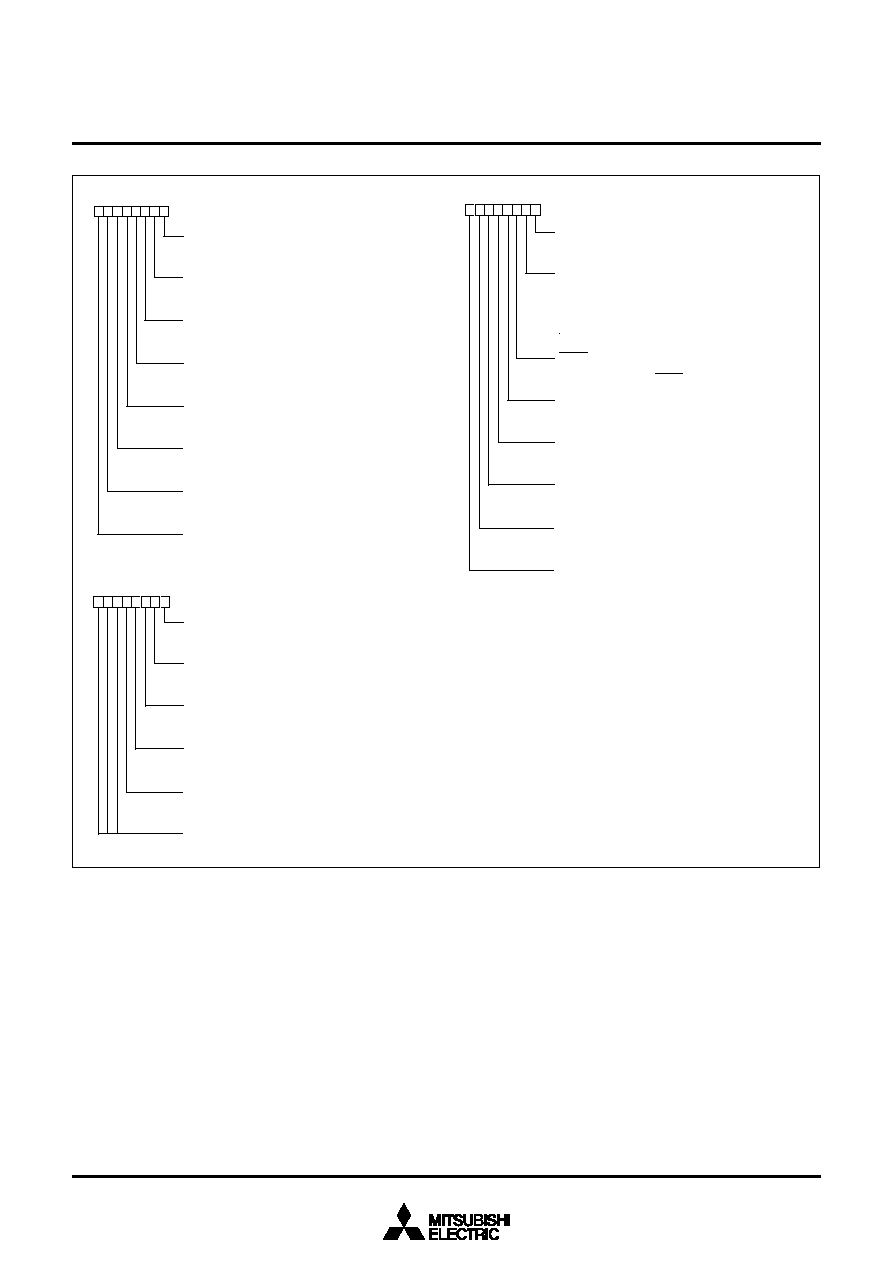
29
3886 Group
SINGLE-CHIP 8-BIT CMOS MICROCOMPUTER
MITSUBISHI MICROCOMPUTERS
Fig. 25 Structure of serial I/O1 control registers
b
7
b
7
T
r
a
n
s
m
i
t
b
u
f
f
e
r
e
m
p
t
y
f
l
a
g
(
T
B
E
)
0
:
B
u
f
f
e
r
f
u
l
l
1
:
B
u
f
f
e
r
e
m
p
t
y
R
e
c
e
i
v
e
b
u
f
f
e
r
f
u
l
l
f
l
a
g
(
R
B
F
)
0
:
B
u
f
f
e
r
e
m
p
t
y
1
:
B
u
f
f
e
r
f
u
l
l
T
r
a
n
s
m
i
t
s
h
i
f
t
c
o
m
p
l
e
t
i
o
n
f
l
a
g
(
T
S
C
)
0
:
T
r
a
n
s
m
i
t
s
h
i
f
t
i
n
p
r
o
g
r
e
s
s
1
:
T
r
a
n
s
m
i
t
s
h
i
f
t
c
o
m
p
l
e
t
e
d
O
v
e
r
r
u
n
e
r
r
o
r
f
l
a
g
(
O
E
)
0
:
N
o
e
r
r
o
r
1
:
O
v
e
r
r
u
n
e
r
r
o
r
P
a
r
i
t
y
e
r
r
o
r
f
l
a
g
(
P
E
)
0
:
N
o
e
r
r
o
r
1
:
P
a
r
i
t
y
e
r
r
o
r
F
r
a
m
i
n
g
e
r
r
o
r
f
l
a
g
(
F
E
)
0
:
N
o
e
r
r
o
r
1
:
F
r
a
m
i
n
g
e
r
r
o
r
S
u
m
m
i
n
g
e
r
r
o
r
f
l
a
g
(
S
E
)
0
:
(
O
E
)
U
(
P
E
)
U
(
F
E
)
=
0
1
:
(
O
E
)
U
(
P
E
)
U
(
F
E
)
=
1
N
o
t
u
s
e
d
(
r
e
t
u
r
n
s
"
1
"
w
h
e
n
r
e
a
d
)
S
e
r
i
a
l
I
/
O
1
s
t
a
t
u
s
r
e
g
i
s
t
e
r
S
e
r
i
a
l
I
/
O
1
c
o
n
t
r
o
l
r
e
g
i
s
t
e
r
b
0
b
0
B
R
G
c
o
u
n
t
s
o
u
r
c
e
s
e
l
e
c
t
i
o
n
b
i
t
(
C
S
S
)
0
:
f
(
X
I
N
)
(
f
(
X
C
I
N
)
i
n
l
o
w
-
s
p
e
e
d
m
o
d
e
)
1
:
f
(
X
I
N
)
/
4
(
f
(
X
C
I
N
)
/
4
i
n
l
o
w
-
s
p
e
e
d
m
o
d
e
)
S
e
r
i
a
l
I
/
O
1
s
y
n
c
h
r
o
n
o
u
s
c
l
o
c
k
s
e
l
e
c
t
i
o
n
b
i
t
(
S
C
S
)
0
:
B
R
G
o
u
t
p
u
t
d
i
v
i
d
e
d
b
y
4
w
h
e
n
c
l
o
c
k
s
y
n
c
h
r
o
n
o
u
s
s
e
r
i
a
l
I
/
O
i
s
s
e
l
e
c
t
e
d
,
B
R
G
o
u
t
p
u
t
d
i
v
i
d
e
d
b
y
1
6
w
h
e
n
U
A
R
T
i
s
s
e
l
e
c
t
e
d
.
1
:
E
x
t
e
r
n
a
l
c
l
o
c
k
i
n
p
u
t
w
h
e
n
c
l
o
c
k
s
y
n
c
h
r
o
n
o
u
s
s
e
r
i
a
l
I
/
O
i
s
s
e
l
e
c
t
e
d
,
e
x
t
e
r
n
a
l
c
l
o
c
k
i
n
p
u
t
d
i
v
i
d
e
d
b
y
1
6
w
h
e
n
U
A
R
T
i
s
s
e
l
e
c
t
e
d
.
S
R
D
Y
1
o
u
t
p
u
t
e
n
a
b
l
e
b
i
t
(
S
R
D
Y
)
0
:
P
4
7
p
i
n
o
p
e
r
a
t
e
s
a
s
o
r
d
i
n
a
r
y
I
/
O
p
i
n
1
:
P
4
7
p
i
n
o
p
e
r
a
t
e
s
a
s
S
R
D
Y
1
o
u
t
p
u
t
p
i
n
T
r
a
n
s
m
i
t
i
n
t
e
r
r
u
p
t
s
o
u
r
c
e
s
e
l
e
c
t
i
o
n
b
i
t
(
T
I
C
)
0
:
I
n
t
e
r
r
u
p
t
w
h
e
n
t
r
a
n
s
m
i
t
b
u
f
f
e
r
h
a
s
e
m
p
t
i
e
d
1
:
I
n
t
e
r
r
u
p
t
w
h
e
n
t
r
a
n
s
m
i
t
s
h
i
f
t
o
p
e
r
a
t
i
o
n
i
s
c
o
m
p
l
e
t
e
d
T
r
a
n
s
m
i
t
e
n
a
b
l
e
b
i
t
(
T
E
)
0
:
T
r
a
n
s
m
i
t
d
i
s
a
b
l
e
d
1
:
T
r
a
n
s
m
i
t
e
n
a
b
l
e
d
R
e
c
e
i
v
e
e
n
a
b
l
e
b
i
t
(
R
E
)
0
:
R
e
c
e
i
v
e
d
i
s
a
b
l
e
d
1
:
R
e
c
e
i
v
e
e
n
a
b
l
e
d
S
e
r
i
a
l
I
/
O
1
m
o
d
e
s
e
l
e
c
t
i
o
n
b
i
t
(
S
I
O
M
)
0
:
C
l
o
c
k
a
s
y
n
c
h
r
o
n
o
u
s
(
U
A
R
T
)
s
e
r
i
a
l
I
/
O
1
:
C
l
o
c
k
s
y
n
c
h
r
o
n
o
u
s
s
e
r
i
a
l
I
/
O
S
e
r
i
a
l
I
/
O
1
e
n
a
b
l
e
b
i
t
(
S
I
O
E
)
0
:
S
e
r
i
a
l
I
/
O
d
i
s
a
b
l
e
d
(
p
i
n
s
P
4
4
t
o
P
4
7
o
p
e
r
a
t
e
a
s
o
r
d
i
n
a
r
y
I
/
O
p
i
n
s
)
1
:
S
e
r
i
a
l
I
/
O
e
n
a
b
l
e
d
(
p
i
n
s
P
4
4
t
o
P
4
7
o
p
e
r
a
t
e
a
s
s
e
r
i
a
l
I
/
O
p
i
n
s
)
b
7
U
A
R
T
c
o
n
t
r
o
l
r
e
g
i
s
t
e
r
C
h
a
r
a
c
t
e
r
l
e
n
g
t
h
s
e
l
e
c
t
i
o
n
b
i
t
(
C
H
A
S
)
0
:
8
b
i
t
s
1
:
7
b
i
t
s
P
a
r
i
t
y
e
n
a
b
l
e
b
i
t
(
P
A
R
E
)
0
:
P
a
r
i
t
y
c
h
e
c
k
i
n
g
d
i
s
a
b
l
e
d
1
:
P
a
r
i
t
y
c
h
e
c
k
i
n
g
e
n
a
b
l
e
d
P
a
r
i
t
y
s
e
l
e
c
t
i
o
n
b
i
t
(
P
A
R
S
)
0
:
E
v
e
n
p
a
r
i
t
y
1
:
O
d
d
p
a
r
i
t
y
S
t
o
p
b
i
t
l
e
n
g
t
h
s
e
l
e
c
t
i
o
n
b
i
t
(
S
T
P
S
)
0
:
1
s
t
o
p
b
i
t
1
:
2
s
t
o
p
b
i
t
s
P
4
5
/
T
X
D
P
-
c
h
a
n
n
e
l
o
u
t
p
u
t
d
i
s
a
b
l
e
b
i
t
(
P
O
F
F
)
0
:
C
M
O
S
o
u
t
p
u
t
(
i
n
o
u
t
p
u
t
m
o
d
e
)
1
:
N
-
c
h
a
n
n
e
l
o
p
e
n
d
r
a
i
n
o
u
t
p
u
t
(
i
n
o
u
t
p
u
t
m
o
d
e
)
N
o
t
u
s
e
d
(
r
e
t
u
r
n
"
1
"
w
h
e
n
r
e
a
d
)
b
0
(
S
I
O
1
S
T
S
:
a
d
d
r
e
s
s
0
0
1
9
1
6
)
(
S
I
O
1
C
O
N
:
a
d
d
r
e
s
s
0
0
1
A
1
6
)
(
U
A
R
T
C
O
N
:
a
d
d
r
e
s
s
0
0
1
B
1
6
)
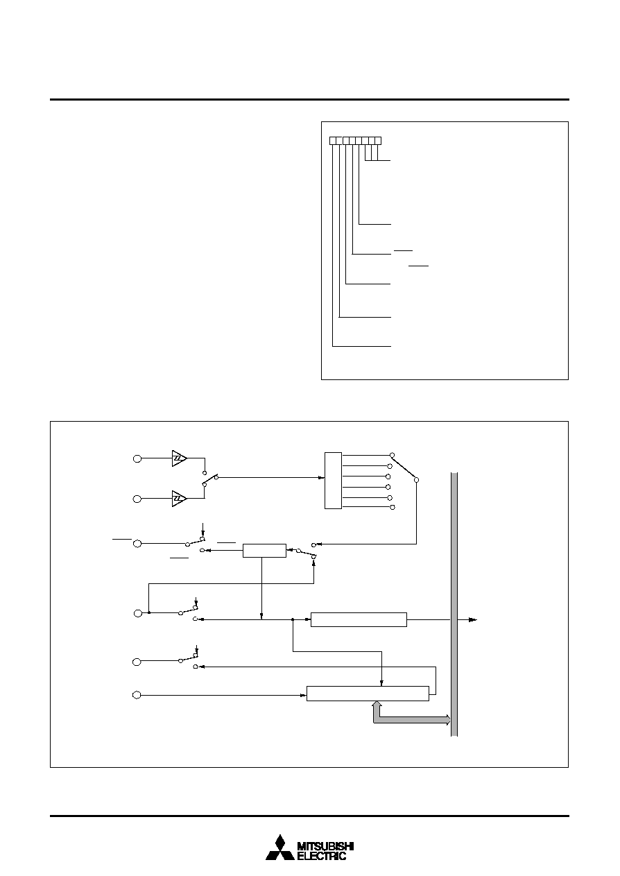
30
3886 Group
SINGLE-CHIP 8-BIT CMOS MICROCOMPUTER
MITSUBISHI MICROCOMPUTERS
Serial I/O2
The serial I/O2 function can be used only for clock synchronous
serial I/O.
For clock synchronous serial I/O the transmitter and the receiver
must use the same clock. If the internal clock is used, transfer is
started by a write signal to the serial I/O2 register.
[Serial I/O2 Control Register (SIO2CON)]
001D
16
The serial I/O2 control register contains seven bits which control
various serial I/O functions.
Fig. 26 Structure of serial I/O2 control register
Fig. 27 Block diagram of serial I/O2 function
S
e
r
i
a
l
I
/
O
2
c
o
n
t
r
o
l
r
e
g
i
s
t
e
r
(
S
I
O
2
C
O
N
:
a
d
d
r
e
s
s
0
0
1
D
1
6
)
b
7
I
n
t
e
r
n
a
l
s
y
n
c
h
r
o
n
o
u
s
c
l
o
c
k
s
e
l
e
c
t
i
o
n
b
i
t
s
0
0
0
:
f
(
X
I
N
)
/
8
(
f
(
X
C
I
N
)
/
8
i
n
l
o
w
-
s
p
e
e
d
m
o
d
e
)
0
0
1
:
f
(
X
I
N
)
/
1
6
(
f
(
X
C
I
N
)
/
1
6
i
n
l
o
w
-
s
p
e
e
d
m
o
d
e
)
0
1
0
:
f
(
X
I
N
)
/
3
2
(
f
(
X
C
I
N
)
/
3
2
i
n
l
o
w
-
s
p
e
e
d
m
o
d
e
)
0
1
1
:
f
(
X
I
N
)
/
6
4
(
f
(
X
C
I
N
)
/
6
4
i
n
l
o
w
-
s
p
e
e
d
m
o
d
e
)
1
1
0
:
f
(
X
I
N
)
/
1
2
8
(
f
(
X
C
I
N
)
/
1
2
8
i
n
l
o
w
-
s
p
e
e
d
m
o
d
e
)
1
1
1
:
f
(
X
I
N
)
/
2
5
6
(
f
(
X
C
I
N
)
/
2
5
6
i
n
l
o
w
-
s
p
e
e
d
m
o
d
e
)
S
e
r
i
a
l
I
/
O
2
p
o
r
t
s
e
l
e
c
t
i
o
n
b
i
t
0
:
I
/
O
p
o
r
t
1
:
S
O
U
T
2
,
S
C
L
K
2
s
i
g
n
a
l
o
u
t
p
u
t
S
R
D
Y
2
o
u
t
p
u
t
e
n
a
b
l
e
b
i
t
0
:
I
/
O
p
o
r
t
1
:
S
R
D
Y
2
s
i
g
n
a
l
o
u
t
p
u
t
T
r
a
n
s
f
e
r
d
i
r
e
c
t
i
o
n
s
e
l
e
c
t
i
o
n
b
i
t
0
:
L
S
B
f
i
r
s
t
1
:
M
S
B
f
i
r
s
t
S
e
r
i
a
l
I
/
O
2
s
y
n
c
h
r
o
n
o
u
s
c
l
o
c
k
s
e
l
e
c
t
i
o
n
b
i
t
0
:
E
x
t
e
r
n
a
l
c
l
o
c
k
1
:
I
n
t
e
r
n
a
l
c
l
o
c
k
C
o
m
p
a
r
a
t
o
r
r
e
f
e
r
e
n
c
e
i
n
p
u
t
s
e
l
e
c
t
i
o
n
b
i
t
0
:
P
0
0
/
P
3
R
E
F
i
n
p
u
t
1
:
R
e
f
e
r
e
n
c
e
i
n
p
u
t
f
i
x
e
d
b
0
b
2
b
1
b
0
X
I
N
"
1
"
"
0
"
"
0
"
"
1
"
"
0
"
"
1
"
S
R
D
Y
2
S
C
L
K
2
"
0
"
"
1
"
1
/
8
1
/
1
6
1
/
3
2
1
/
6
4
1
/
1
2
8
1
/
2
5
6
X
C
I
N
"
1
0
"
"
0
0
"
"
0
1
"
D
a
t
a
b
u
s
S
e
r
i
a
l
I
/
O
2
i
n
t
e
r
r
u
p
t
r
e
q
u
e
s
t
S
e
r
i
a
l
I
/
O
2
p
o
r
t
s
e
l
e
c
t
i
o
n
b
i
t
S
e
r
i
a
l
I
/
O
c
o
u
n
t
e
r
2
(
3
)
S
e
r
i
a
l
I
/
O
2
r
e
g
i
s
t
e
r
(
8
)
S
y
n
c
h
r
o
n
i
z
a
t
i
o
n
c
i
r
c
u
i
t
S
e
r
i
a
l
I
/
O
2
p
o
r
t
s
e
l
e
c
t
i
o
n
b
i
t
S
e
r
i
a
l
I
/
O
2
s
y
n
c
h
r
o
n
o
u
s
c
l
o
c
k
s
e
l
e
c
t
i
o
n
b
i
t
S
R
D
Y
2
o
u
t
p
u
t
e
n
a
b
l
e
b
i
t
E
x
t
e
r
n
a
l
c
l
o
c
k
I
n
t
e
r
n
a
l
s
y
n
c
h
r
o
n
o
u
s
c
l
o
c
k
s
e
l
e
c
t
i
o
n
b
i
t
s
D
i
v
i
d
e
r
P
7
2
/
S
C
L
K
2
P
7
1
/
S
O
U
T
2
P
7
0
/
S
I
N
2
P
7
2
l
a
t
c
h
P
7
1
l
a
t
c
h
P
7
3
l
a
t
c
h
P
7
3
/
S
R
D
Y
2
/
I
N
T
2
1
M
a
i
n
c
l
o
c
k
d
i
v
i
d
e
r
a
t
i
o
s
e
l
e
c
t
i
o
n
b
i
t
s
(
N
o
t
e
)
N
o
t
e
:
T
h
e
s
e
b
i
t
s
s
e
l
e
c
t
a
n
y
o
f
t
h
e
h
i
g
h
-
s
p
e
e
d
m
o
d
e
,
t
h
e
m
i
d
d
l
e
-
s
p
e
e
d
m
o
d
e
,
a
n
d
t
h
e
l
o
w
-
s
p
e
e
d
m
o
d
e
.
T
h
e
s
e
a
r
e
a
s
s
i
g
n
e
d
t
o
b
i
t
s
7
a
n
d
6
o
f
t
h
e
C
P
U
m
o
d
e
r
e
g
i
s
t
e
r
(
a
d
d
r
e
s
s
0
0
3
B
1
6
)
.
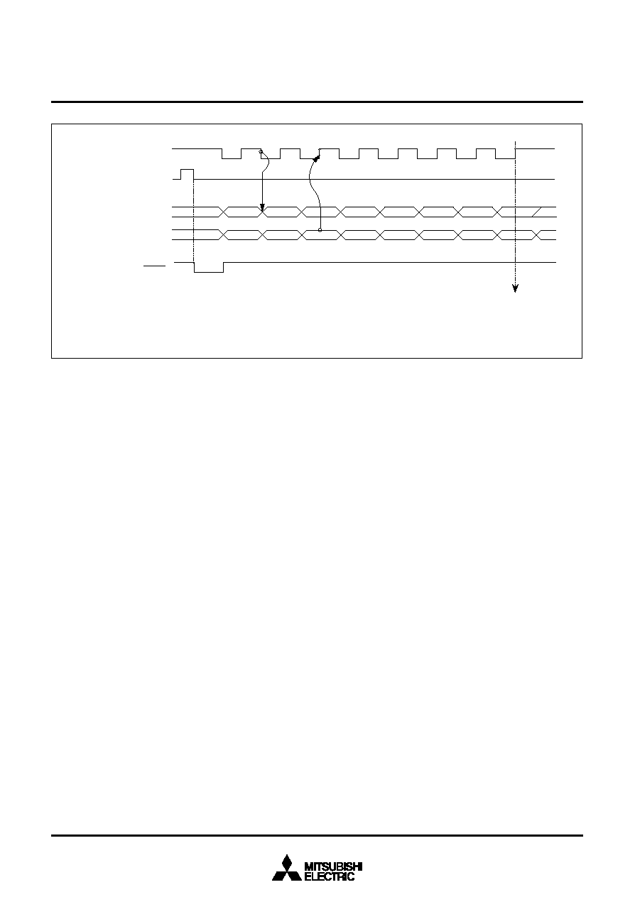
31
3886 Group
SINGLE-CHIP 8-BIT CMOS MICROCOMPUTER
MITSUBISHI MICROCOMPUTERS
Fig. 28 Timing of serial I/O2 function
D
7
D
0
D
1
D
2
D
3
D
4
D
5
D
6
T
r
a
n
s
f
e
r
c
l
o
c
k
(
N
o
t
e
1
)
S
e
r
i
a
l
I
/
O
2
o
u
t
p
u
t
S
O
U
T
2
S
e
r
i
a
l
I
/
O
2
i
n
p
u
t
S
I
N
2
R
e
c
e
i
v
e
e
n
a
b
l
e
s
i
g
n
a
l
S
R
D
Y
2
S
e
r
i
a
l
I
/
O
2
r
e
g
i
s
t
e
r
w
r
i
t
e
s
i
g
n
a
l
(
N
o
t
e
2
)
S
e
r
i
a
l
I
/
O
2
i
n
t
e
r
r
u
p
t
r
e
q
u
e
s
t
b
i
t
s
e
t
1
:
W
h
e
n
t
h
e
i
n
t
e
r
n
a
l
c
l
o
c
k
i
s
s
e
l
e
c
t
e
d
a
s
t
h
e
t
r
a
n
s
f
e
r
c
l
o
c
k
,
t
h
e
d
i
v
i
d
e
r
a
t
i
o
c
a
n
b
e
s
e
l
e
c
t
e
d
b
y
s
e
t
t
i
n
g
b
i
t
s
0
t
o
2
o
f
t
h
e
s
e
r
i
a
l
I
/
O
2
c
o
n
t
r
o
l
r
e
g
i
s
t
e
r
.
2
:
W
h
e
n
t
h
e
i
n
t
e
r
n
a
l
c
l
o
c
k
i
s
s
e
l
e
c
t
e
d
a
s
t
h
e
t
r
a
n
s
f
e
r
c
l
o
c
k
,
t
h
e
S
O
U
T
2
p
i
n
g
o
e
s
t
o
h
i
g
h
i
m
p
e
d
a
n
c
e
a
f
t
e
r
t
r
a
n
s
f
e
r
c
o
m
p
l
e
t
i
o
n
.
N
o
t
e
s
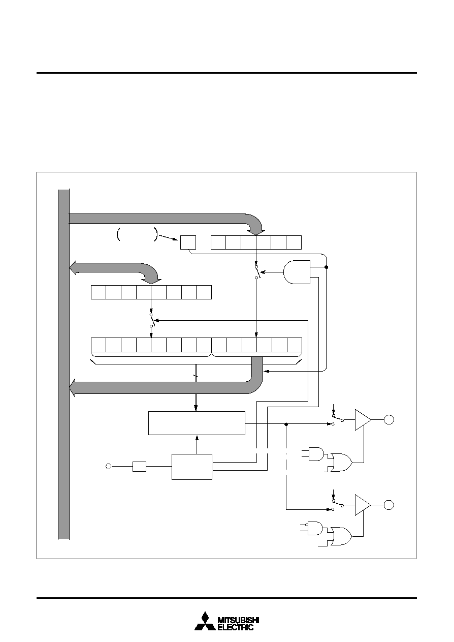
32
3886 Group
SINGLE-CHIP 8-BIT CMOS MICROCOMPUTER
MITSUBISHI MICROCOMPUTERS
PULSE WIDTH MODULATION (PWM)
OUTPUT CIRCUIT
The 3886 group has two PWM output circuits, PWM0 and PWM1,
with 14-bit resolution respectively. These can operate indepen-
dently. When the oscillation frequency X
IN
is 10 MHz, the
minimum resolution bit width is 200 ns and the cycle period is
3276.8
µ
s. The PWM timing generator supplies a PWM control
signal based on a signal that is the frequency of the X
IN
clock.
Fig. 29 PWM block diagram (PWM0)
The following explanation assumes f(X
IN
) = 8 MHz.
1
4
1
/
2
P
W
M
0
e
n
a
b
l
e
b
i
t
P
3
0
l
a
t
c
h
P
3
0
/
P
W
M
0
0
P
W
M
0
L
r
e
g
i
s
t
e
r
(
a
d
d
r
e
s
s
0
0
3
1
1
6
)
P
W
M
0
H
r
e
g
i
s
t
e
r
(
a
d
d
r
e
s
s
0
0
3
0
1
6
)
b
i
t
7
b
i
t
0
b
i
t
5
M
S
B
L
S
B
P
W
M
0
b
i
t
7
b
i
t
0
P
W
M
0
t
i
m
i
n
g
g
e
n
e
r
a
t
o
r
(
6
4
µ
s
p
e
r
i
o
d
)
(
4
0
9
6
µ
s
p
e
r
i
o
d
)
P
W
M
0
l
a
t
c
h
(
1
4
b
i
t
s
)
S
e
t
t
o
"
1
"
a
t
w
r
i
t
e
D
a
t
a
B
u
s
f
(
X
I
N
)
(
8
M
H
z
)
1
4
-
b
i
t
P
W
M
0
c
i
r
c
u
i
t
P
5
6
d
i
r
e
c
t
i
o
n
r
e
g
i
s
t
e
r
P
W
M
0
e
n
a
b
l
e
b
i
t
P
W
M
0
e
n
a
b
l
e
b
i
t
P
5
6
l
a
t
c
h
P
5
6
/
D
A
1
/
P
W
M
0
1
P
W
M
0
o
u
t
p
u
t
s
e
l
e
c
t
i
o
n
b
i
t
P
3
0
d
i
r
e
c
t
i
o
n
r
e
g
i
s
t
e
r
(
4
M
H
z
)
P
W
M
0
e
n
a
b
l
e
b
i
t
P
W
M
0
o
u
t
p
u
t
s
e
l
e
c
t
i
o
n
b
i
t
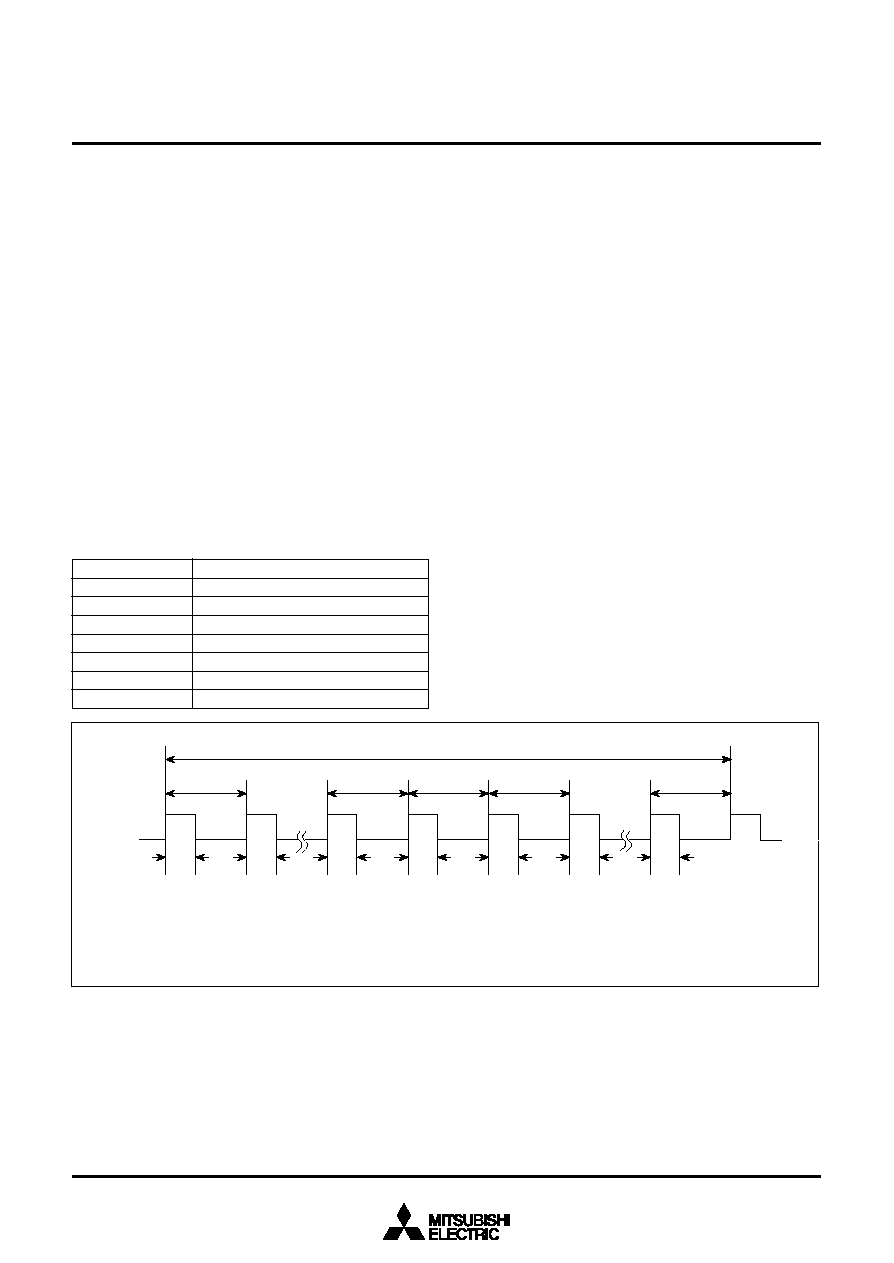
33
3886 Group
SINGLE-CHIP 8-BIT CMOS MICROCOMPUTER
MITSUBISHI MICROCOMPUTERS
Data Setup (PWM0)
The PWM0 output pin also functions as port P3
0
or P5
6
. The
PWM0 output pin is selected from either P3
0
/PWM
00
or
P5
6
/PWM
01
by bit 4 of the AD/DA control register (address
0034
16
).
The PWM0 output becomes enabled state by setting bit 6 of the
port control register 1 (address 002E
16
). The high-order eight bits
of output data are set in the PWM0H register (address 0030
16
)
and the low-order six bits are set in the PWM0L register (address
0031
16
).
PWM1 is set as the same way.
PWM Operation
The 14-bit PWM data is divided into the low-order six bits and the
high-order eight bits in the PWM latch.
The high-order eight bits of data determine how long an "H"-level
signal is output during each sub-period. There are 64 sub-periods
in each period, and each sub-period is 256
!
(64
µ
s) long. The
signal is "H" for a length equal to N times
, where
is the mini-
mum resolution (250 ns).
"H" or "L" of the bit in the ADD part shown in Figure 30 is added to
this "H" duration by the contents of the low-order 6-bit data accord-
ing to the rule in Table 7.
That is, only in the sub-period tm shown by Table 7 in the PWM
cycle period T = 64t, its "H" duration is lengthened to the minimum
resolution
added to the length of other periods.
For example, if the high-order eight bits of the 14-bit data are 03
16
and the low-order six bits are 05
16
, the length of the "H"-level out-
put in sub-periods t
8
, t
24
, t
32
, t
40
, and t
56
is 4
, and its length is 3
in all other sub-periods.
Time at the "H" level of each sub-period almost becomes equal,
because the time becomes length set in the high-order 8 bits or
becomes the value plus
, and this sub-period t (= 64
µ
s, approxi-
mate 15.6 kHz) becomes cycle period approximately.
Transfer From Register to Latch
Data written to the PWML register is transferred to the PWM latch
at each PWM period (every 4096
µ
s), and data written to the
PWMH register is transferred to the PWM latch at each sub-period
(every 64
µ
s). The signal which is output to the PWM output pin is
corresponding to the contents of this latch. When the PWML regis-
ter is read, the latch contents are read. However, bit 7 of the
PWML register indicates whether the transfer to the PWM latch is
completed; the transfer is completed when bit 7 is "0" and it is not
done when bit 7 is "1."
Table 7 Relationship between low-order 6 bits of data and
period set by the ADD bit
Low-order 6 bits of data (PWML)
LSB
0 0 0 0 0 0
0 0 0 0 0 1
0 0 0 0 1 0
0 0 0 1 0 0
0 0 1 0 0 0
0 1 0 0 0 0
1 0 0 0 0 0
Sub-periods tm Lengthened (m=0 to 63)
None
m=32
m=16, 48
m=8, 24, 40, 56
m=4, 12, 20, 28, 36, 44, 52, 60
m=2, 6, 10, 14, 18, 22, 26, 30, 34, 38, 42, 46, 50, 54, 58, 62
m=1, 3, 5, 7, ................................................ ,57, 59, 61, 63
Fig. 30 PWM timing
4
0
9
6
µ
s
6
4
µ
s
6
4
µ
s
6
4
µ
s
6
4
µ
s
6
4
µ
s
m
=
0
m
=
7
m
=
9
m
=
6
3
m
=
8
1
5
.
7
5
µ
s
1
5
.
7
5
µ
s
1
5
.
7
5
µ
s
1
6
.
0
µ
s
1
5
.
7
5
µ
s
1
5
.
7
5
µ
s
1
5
.
7
5
µ
s
P
u
l
s
e
w
i
d
t
h
m
o
d
u
l
a
t
i
o
n
r
e
g
i
s
t
e
r
H
P
u
l
s
e
w
i
d
t
h
m
o
d
u
l
a
t
i
o
n
r
e
g
i
s
t
e
r
L
S
u
b
-
p
e
r
i
o
d
s
w
h
e
r
e
"
H
"
p
u
l
s
e
w
i
d
t
h
i
s
1
6
.
0
µ
s
:
S
u
b
-
p
e
r
i
o
d
s
w
h
e
r
e
"
H
"
p
u
l
s
e
w
i
d
t
h
i
s
1
5
.
7
5
µ
s
:
:
0
0
1
1
1
1
1
1
:
0
0
0
1
0
1
m
=
8
,
2
4
,
3
2
,
4
0
,
5
6
m
=
a
l
l
o
t
h
e
r
v
a
l
u
e
s
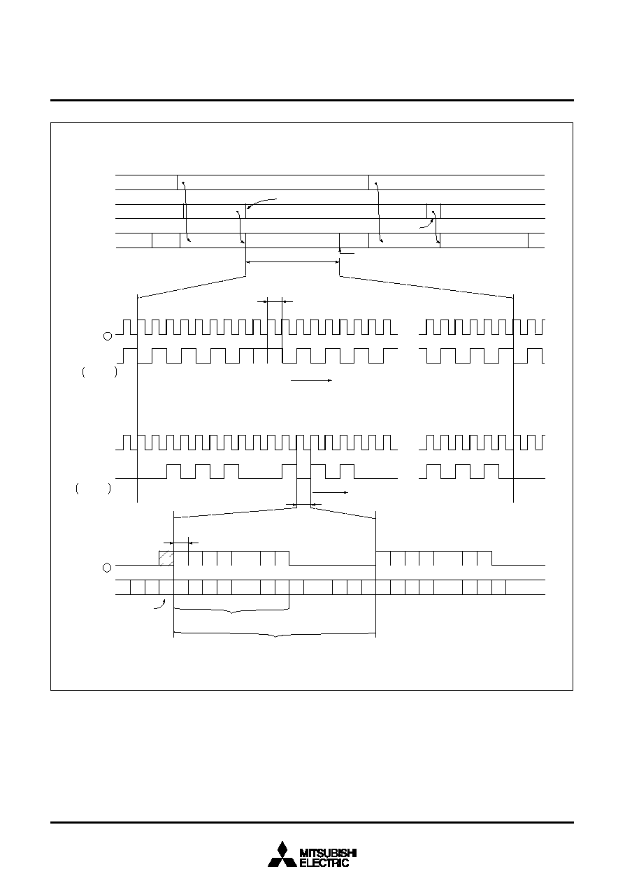
34
3886 Group
SINGLE-CHIP 8-BIT CMOS MICROCOMPUTER
MITSUBISHI MICROCOMPUTERS
Fig. 31 14-bit PWM timing (PWM
0
)
6
A
6
A
6
A
6
A
6
A
6
B
6
A
6
A
6
A
6
A
6
A
6
A
6
A
6
A
6
B
6
B
6
B
6
B
6
B
6
B
6
B
6
B
6
B
6
B
6
B
6
B
6
B
5
5
5
5
5
5
5
5
5
5
5
5
5
5
6
A
6
A
6
B
6
B
6
B
6
A
6
B
6
B
6
B
6
A
6
B
6
B
6
B
6
A
6
A
6
A
6
A
6
A
6
A
6
A
6
A
6
A
6
A
6
A
6
A
6
A
6
A
4
3
4
4
3
4
4
3
4
6
B
6
A
6
9
6
8
6
7
0
2
0
1
6
A
6
9
6
8
6
7
0
2
0
1
0
2
0
1
0
0
F
F
F
E
F
D
9
7
9
6
9
5
0
2
0
1
0
0
F
C
F
F
F
E
F
D
9
7
9
6
9
5
F
C
A
D
D
A
D
D
1
6
5
3
1
6
1
A
9
3
1
6
1
A
A
4
1
6
1
A
A
4
1
6
1
E
E
4
1
6
1
E
F
5
1
6
T
=
4
0
9
6
µ
s
(
6
4
!
6
4
µ
s
)
t
=
6
4
µ
s
W
h
e
n
b
i
t
7
o
f
P
W
M
0
L
i
s
0
,
t
r
a
n
s
f
e
r
f
r
o
m
r
e
g
i
s
t
e
r
t
o
l
a
t
c
h
i
s
d
i
s
a
b
l
e
d
.
1
3
1
6
A
4
1
6
2
4
1
6
3
5
1
6
7
B
1
6
6
A
1
6
5
9
1
6
D
a
t
a
2
4
1
6
s
t
o
r
e
d
a
t
a
d
d
r
e
s
s
0
0
3
1
1
6
D
a
t
a
6
A
1
6
s
t
o
r
e
d
a
t
a
d
d
r
e
s
s
0
0
3
0
1
6
D
a
t
a
7
B
1
6
s
t
o
r
e
d
a
t
a
d
d
r
e
s
s
0
0
3
0
1
6
D
a
t
a
3
5
1
6
s
t
o
r
e
d
a
t
a
d
d
r
e
s
s
0
0
3
1
1
6
T
r
a
n
s
f
e
r
f
r
o
m
r
e
g
i
s
t
e
r
t
o
l
a
t
c
h
T
r
a
n
s
f
e
r
f
r
o
m
r
e
g
i
s
t
e
r
t
o
l
a
t
c
h
B
i
t
7
c
l
e
a
r
e
d
a
f
t
e
r
t
r
a
n
s
f
e
r
6
B
1
6
∑
∑
∑
∑
∑
∑
∑
∑
∑
∑
∑
∑
∑
∑
3
6
t
i
m
e
s
6
A
1
6
∑
∑
∑
∑
∑
∑
∑
∑
∑
∑
∑
∑
∑
2
8
t
i
m
e
s
(
1
0
7
)
(
1
0
6
)
6
B
1
6
∑
∑
∑
∑
∑
∑
∑
∑
∑
∑
∑
∑
∑
∑
2
4
t
i
m
e
s
6
A
1
6
∑
∑
∑
∑
∑
∑
∑
4
0
t
i
m
e
s
t
=
6
4
µ
s
(
2
5
6
!
0
.
2
5
µ
s
)
M
i
n
i
m
u
m
r
e
s
o
l
u
t
i
o
n
b
i
t
w
i
d
t
h
=
0
.
2
5
µ
s
H
d
u
r
a
t
i
o
n
l
e
n
g
t
h
s
p
e
c
i
f
i
e
d
b
y
P
W
M
0
H
2
5
6
(
6
4
µ
s
)
,
f
i
x
e
d
T
h
e
A
D
D
p
o
r
t
i
o
n
s
w
i
t
h
a
d
d
i
t
i
o
n
a
l
a
r
e
d
e
t
e
r
m
i
n
e
d
b
y
P
W
M
L
.
P
W
M
0
H
r
e
g
i
s
t
e
r
P
W
M
0
L
r
e
g
i
s
t
e
r
P
W
M
0
l
a
t
c
h
(
1
4
b
i
t
s
)
E
x
a
m
p
l
e
1
P
W
M
0
o
u
t
p
u
t
l
o
w
-
o
r
d
e
r
6
-
b
i
t
o
u
t
p
u
t
:
H
L
6
A
1
6
,
2
4
1
6
E
x
a
m
p
l
e
2
P
W
M
0
o
u
t
p
u
t
l
o
w
-
o
r
d
e
r
6
-
b
i
t
o
u
t
p
u
t
:
H
L
6
A
1
6
,
1
8
1
6
P
W
M
o
u
t
p
u
t
8
-
b
i
t
c
o
u
n
t
e
r
1
0
6
!
6
4
+
2
4
1
2
B
5
1
6
1
0
6
!
6
4
+
3
6
2
∑
∑
∑
∑
∑
∑
∑
∑
∑
∑
∑
∑
∑
∑
∑
∑
∑
∑
∑
∑
∑
∑
∑
∑
∑
∑
∑
∑
∑
∑
∑
∑
∑
∑
∑
∑
∑
∑
∑
∑
∑
∑

35
3886 Group
SINGLE-CHIP 8-BIT CMOS MICROCOMPUTER
MITSUBISHI MICROCOMPUTERS
BUS INTERFACE
The 3886 group has a 2-byte bus interface function which is al-
most functionally equal to MELPS8-41 series and the control
signal from the host CPU side can operate it (slave mode).
It is possible to connect the 3886 group with the RD and WR
separated CPU bus directly. Figure 34 shows the block diagram of
the bus interface function.
The data bus buffer function I/O pins (P4
2
, P4
3
, P4
6
, P4
7
, P5
0
≠
P5
3
, P8) also function as the normal digital port I/O pins. When bit
0 (data bus buffer enable bit) of the data bus buffer control regis-
ter (address 002A
16
) is "0," these pins become the normal digital
port I/O pins. When it is "1," these bits become the data bus buffer
function I/O pins.
The selection of either the single data bus buffer mode, which
uses 1 byte: data bus buffer 0 only, or the double data bus buffer
mode, which uses 2 bytes: data bus buffer 0 and data bus buffer
1, is performed by bit 1 (data bus buffer function selection bit) of
the data bus buffer control register (address 002A
16
). Port P4
7
be-
comes S
1
input in the double data bus buffer mode. When data is
written from the host CPU side, an input buffer full interrupt oc-
curs. When data is read from the host CPU, an output buffer
empty interrupt occurs. This microcomputer shares two input
buffer full interrupt requests and two output buffer empty interrupt
requests as shown in Figure 32, respectively.
Fig. 32 Interrupt request circuit of data bus buffer
I
n
p
u
t
b
u
f
f
e
r
f
u
l
l
f
l
a
g
0
I
B
F
0
I
n
p
u
t
b
u
f
f
e
r
f
u
l
l
f
l
a
g
1
I
B
F
1
R
i
s
i
n
g
e
d
g
e
d
e
t
e
c
t
i
o
n
c
i
r
c
u
i
t
O
n
e
-
s
h
o
t
p
u
l
s
e
g
e
n
e
r
a
t
i
n
g
c
i
r
c
u
i
t
O
n
e
-
s
h
o
t
p
u
l
s
e
g
e
n
e
r
a
t
i
n
g
c
i
r
c
u
i
t
I
n
p
u
t
b
u
f
f
e
r
f
u
l
l
i
n
t
e
r
r
u
p
t
r
e
q
u
e
s
t
s
i
g
n
a
l
I
B
F
O
u
t
p
u
t
b
u
f
f
e
r
f
u
l
l
f
l
a
g
0
O
B
F
0
O
u
t
p
u
t
b
u
f
f
e
r
f
u
l
l
f
l
a
g
1
O
B
F
1
O
n
e
-
s
h
o
t
p
u
l
s
e
g
e
n
e
r
a
t
i
n
g
c
i
r
c
u
i
t
O
n
e
-
s
h
o
t
p
u
l
s
e
g
e
n
e
r
a
t
i
n
g
c
i
r
c
u
i
t
O
u
t
p
u
t
b
u
f
f
e
r
e
m
p
t
y
i
n
t
e
r
r
u
p
t
r
e
q
u
e
s
t
s
i
g
n
a
l
O
B
E
I
n
t
e
r
r
u
p
t
r
e
q
u
e
s
t
i
s
s
e
t
a
t
t
h
i
s
r
i
s
i
n
g
e
d
g
e
I
n
t
e
r
r
u
p
t
r
e
q
u
e
s
t
i
s
s
e
t
a
t
t
h
i
s
r
i
s
i
n
g
e
d
g
e
I
B
F
0
I
B
F
1
I
B
F
O
B
F
0
(
O
B
E
0
)
O
B
F
1
(
O
B
E
1
)
O
B
E
O
B
E
0
O
B
E
1
R
i
s
i
n
g
e
d
g
e
d
e
t
e
c
t
i
o
n
c
i
r
c
u
i
t
R
i
s
i
n
g
e
d
g
e
d
e
t
e
c
t
i
o
n
c
i
r
c
u
i
t
R
i
s
i
n
g
e
d
g
e
d
e
t
e
c
t
i
o
n
c
i
r
c
u
i
t
36
3886 Group
SINGLE-CHIP 8-BIT CMOS MICROCOMPUTER
MITSUBISHI MICROCOMPUTERS
Fig. 33 Structure of bus interface related register
D
a
t
a
b
u
s
b
u
f
f
e
r
c
o
n
t
r
o
l
r
e
g
i
s
t
e
r
b
0
b
7
D
a
t
a
b
u
s
b
u
f
f
e
r
e
n
a
b
l
e
b
i
t
0
:
P
5
0
≠
P
5
3
,
P
8
I
/
O
p
o
r
t
1
:
D
a
t
a
b
u
s
b
u
f
f
e
r
e
n
a
b
l
e
d
D
a
t
a
b
u
s
b
u
f
f
e
r
f
u
n
c
t
i
o
n
s
e
l
e
c
t
i
o
n
b
i
t
0
:
S
i
n
g
l
e
d
a
t
a
b
u
s
b
u
f
f
e
r
m
o
d
e
(
P
4
7
f
u
n
c
t
i
o
n
s
a
s
I
/
O
p
o
r
t
.
)
1
:
D
o
u
b
l
e
d
a
t
a
b
u
s
b
u
f
f
e
r
m
o
d
e
(
P
4
7
f
u
n
c
t
i
o
n
s
S
1
i
n
p
u
t
.
)
O
B
F
0
o
u
t
p
u
t
s
e
l
e
c
t
i
o
n
b
i
t
0
:
O
B
F
0
0
v
a
l
i
d
1
:
O
B
F
0
1
v
a
l
i
d
O
B
F
0
0
o
u
t
p
u
t
e
n
a
b
l
e
b
i
t
0
:
P
4
2
f
u
n
c
t
i
o
n
s
a
s
p
o
r
t
I
/
O
p
i
n
.
1
:
P
4
2
f
u
n
c
t
i
o
n
s
a
s
O
B
F
0
0
o
u
t
p
u
t
p
i
n
.
O
B
F
0
1
o
u
t
p
u
t
e
n
a
b
l
e
b
i
t
0
:
P
4
3
f
u
n
c
t
i
o
n
s
a
s
p
o
r
t
I
/
O
p
i
n
.
1
:
P
4
3
f
u
n
c
t
i
o
n
s
a
s
O
B
F
0
1
o
u
t
p
u
t
p
i
n
.
O
B
F
1
0
o
u
t
p
u
t
e
n
a
b
l
e
b
i
t
0
:
P
4
6
f
u
n
c
t
i
o
n
s
a
s
p
o
r
t
I
/
O
p
i
n
.
1
:
P
4
6
f
u
n
c
t
i
o
n
s
a
s
O
B
F
1
0
o
u
t
p
u
t
p
i
n
.
I
n
p
u
t
l
e
v
e
l
s
e
l
e
c
t
i
o
n
b
i
t
0
:
C
M
O
S
l
e
v
e
l
i
n
p
u
t
1
:
T
T
L
l
e
v
e
l
i
n
p
u
t
R
e
s
e
r
v
e
d
D
o
n
o
t
w
r
i
t
e
"
1
"
t
o
t
h
i
s
b
i
t
.
D
a
t
a
b
u
s
b
u
f
f
e
r
s
t
a
t
u
s
r
e
g
i
s
t
e
r
1
O
u
t
p
u
t
b
u
f
f
e
r
f
u
l
l
f
l
a
g
1
(
O
B
F
1
)
I
n
p
u
t
b
u
f
f
e
r
f
u
l
l
f
l
a
g
1
(
I
B
F
1
)
U
s
e
r
d
e
f
i
n
a
b
l
e
f
l
a
g
(
U
1
2
)
A
0
1
f
l
a
g
(
A
0
1
)
U
s
e
r
d
e
f
i
n
a
b
l
e
f
l
a
g
(
U
1
4
≠
U
1
7
)
T
h
i
s
f
l
a
g
c
a
n
b
e
d
e
f
i
n
e
d
b
y
u
s
e
r
f
r
e
e
l
y
.
T
h
i
s
f
l
a
g
c
a
n
b
e
d
e
f
i
n
e
d
b
y
u
s
e
r
f
r
e
e
l
y
.
T
h
i
s
f
l
a
g
i
n
d
i
c
a
t
e
s
t
h
e
c
o
n
d
i
t
i
o
n
o
f
A
0
1
s
t
a
t
u
s
w
h
e
n
t
h
e
I
B
F
1
f
l
a
g
i
s
s
e
t
.
0
:
B
u
f
f
e
r
e
m
p
t
y
1
:
B
u
f
f
e
r
f
u
l
l
0
:
B
u
f
f
e
r
e
m
p
t
y
1
:
B
u
f
f
e
r
f
u
l
l
D
a
t
a
b
u
s
b
u
f
f
e
r
s
t
a
t
u
s
r
e
g
i
s
t
e
r
0
O
u
t
p
u
t
b
u
f
f
e
r
f
u
l
l
f
l
a
g
0
(
O
B
F
0
)
I
n
p
u
t
b
u
f
f
e
r
f
u
l
l
f
l
a
g
0
(
I
B
F
0
)
U
s
e
r
d
e
f
i
n
a
b
l
e
f
l
a
g
(
U
0
2
)
A
0
0
f
l
a
g
(
A
0
0
)
T
h
i
s
f
l
a
g
c
a
n
b
e
d
e
f
i
n
e
d
b
y
u
s
e
r
f
r
e
e
l
y
.
T
h
i
s
f
l
a
g
c
a
n
b
e
d
e
f
i
n
e
d
b
y
u
s
e
r
f
r
e
e
l
y
.
T
h
i
s
f
l
a
g
i
n
d
i
c
a
t
e
s
t
h
e
c
o
n
d
i
t
i
o
n
o
f
A
0
0
s
t
a
t
u
s
w
h
e
n
t
h
e
I
B
F
0
f
l
a
g
i
s
s
e
t
.
0
:
B
u
f
f
e
r
e
m
p
t
y
1
:
B
u
f
f
e
r
f
u
l
l
0
:
B
u
f
f
e
r
e
m
p
t
y
1
:
B
u
f
f
e
r
f
u
l
l
b
0
b
7
b
0
b
7
(
D
B
B
C
O
N
:
a
d
d
r
e
s
s
0
0
2
A
1
6
)
(
D
B
B
S
T
S
0
:
a
d
d
r
e
s
s
0
0
2
9
1
6
)
U
s
e
r
d
e
f
i
n
a
b
l
e
f
l
a
g
(
U
0
4
≠
U
0
7
)
(
D
B
B
S
T
S
1
:
a
d
d
r
e
s
s
0
0
2
C
1
6
)
37
3886 Group
SINGLE-CHIP 8-BIT CMOS MICROCOMPUTER
MITSUBISHI MICROCOMPUTERS
Fig. 34 Bus interface device block diagram
P
8
0
/
D
Q
0
R
D
W
R
D
B
B
0
D
B
B
S
T
S
1
b
7
b
6
b
5
b
4
b
3
b
2
b
1
b
0
U
1
7
U
1
6
U
1
5
U
1
4
A
0
1
U
1
2
I
B
F
1
O
B
F
1
U
0
7
U
0
6
U
0
5
U
0
4
A
0
0
U
0
2
I
B
F
0
O
B
F
0
P
8
1
/
D
Q
1
P
8
2
/
D
Q
2
P
8
3
/
D
Q
3
P
8
4
/
D
Q
4
P
8
5
/
D
Q
5
P
8
6
/
D
Q
6
P
8
7
/
D
Q
7
P
5
1
/
I
N
T
2
0
/
S
0
P
5
2
/
I
N
T
3
0
/
R
P
5
3
/
I
N
T
4
0
/
W
P
4
7
/
S
R
D
Y
1
/
S
1
(
A
d
d
r
e
s
s
0
0
2
A
1
6
)
R
D
D
B
B
S
T
S
0
D
B
B
1
W
R
P
4
3
/
I
N
T
1
/
O
B
F
0
1
P
4
2
/
I
N
T
0
/
O
B
F
0
0
P
4
6
/
S
C
L
K
1
/
O
B
F
1
0
(
A
d
d
r
e
s
s
0
0
2
C
1
6
)
(
A
d
d
r
e
s
s
0
0
2
9
1
6
)
I
n
p
u
t
d
a
t
a
b
u
s
b
u
f
f
e
r
0
O
u
t
p
u
t
d
a
t
a
b
u
s
b
u
f
f
e
r
0
O
u
t
p
u
t
d
a
t
a
b
u
s
b
u
f
f
e
r
1
I
n
t
e
r
n
a
l
d
a
t
a
b
u
s
S
y
s
t
e
m
b
u
s
I
n
p
u
t
d
a
t
a
b
u
s
b
u
f
f
e
r
1
P
5
0
/
A
0
(
A
d
d
r
e
s
s
0
0
2
8
1
6
)
(
A
d
d
r
e
s
s
0
0
2
8
1
6
)
(
A
d
d
r
e
s
s
0
0
2
B
1
6
)
(
A
d
d
r
e
s
s
0
0
2
B
1
6
)

38
3886 Group
SINGLE-CHIP 8-BIT CMOS MICROCOMPUTER
MITSUBISHI MICROCOMPUTERS
[Data Bus Buffer Status Register 0, 1
(DBBSTS0, DBBSTS1)] 0029
16
, 002C
16
The data bus buffer status register 0, 1 consist of eight bits.
Bits 0, 1, and 3 are read-only bits and indicate the condition of the
data bus buffer. Bits 2, 4, 5, 6, and 7 are user definable flags
which can be set by program, and can be read/written. This regis-
ter can be read from the host CPU when the A
0
pin is set to "H"
only.
∑Bit 0: Output buffer full flag OBF
0
, OBF
1
When writing data to the output data bus buffer, these flags are
set to "1". When reading the output data bus buffer from the host
CPU, these flags are cleared to "0".
∑Bit 1: Input buffer full flag IBF
0
, IBF
1
When writing data from the host CPU to the input data bus
buffer, these flags are set to "1". When reading the input data
bus buffer from the slave CPU side, these flags are cleared to
"0".
∑Bit 3: A
0
flag A0
0
, A0
1
When writing data from the host CPU to the input data bus
buffer, the level of the A
0
pin is latched.
[Input Data Bus Buffer Register 0, 1 (DBBIN0,
DBBIN1)] 0028
16
, 002B
16
Data on the data bus is latched to DBBIN by writing request from
the host CPU. Data of DBBIN can be read from the data bus
buffer registers (address 0028
16
or 002B
16
) on SFR.
[Output Data Bus Buffer Register 0, 1
(DBBOUT0, DBBOUT1)] 0028
16
, 002B
16
When writing data to the data bus buffer registers (address 0028
16
or 002B
16
) on SFR, data is set to DBBOUT. Data of DBBOUT is
output from the host CPU to the data bus by performing the read-
ing request when the A
0
pin is set to "L".
39
3886 Group
SINGLE-CHIP 8-BIT CMOS MICROCOMPUTER
MITSUBISHI MICROCOMPUTERS
P4
7
/SRDY
1
/S
1
P5
0
/A
0
P5
1
/INT
20
/S
0
P5
2
/INT
30
/R
P5
3
/INT
40
/W
P4
2
/INT
0
/OBF
00
P4
3
/INT
1
/OBF
01
P4
6
/S
CLK1
/OBF
10
Table 8 Function description of control I/O pins at bus interface function selected
Pin
Name
OBF
00
output
enable bit
OBF
01
output
enable bit
OBF
10
output
enable bit
Input
/Output
Functions
S
1
A
0
S
0
R
W
OBF00
OBF01
OBF10
Chip select input
This is used for selecting the data bus buffer and is
selected at "L" level.
Address input
This is used for selecting DBBSTS and DBBOUT
when the host CPU is read.
This is used for distinguishing command from data
when writing to the host CPU.
Chip select input
This is used for selecting the data bus buffer and is
selected at "L" level.
This is a timing signal for reading data from the
data bus buffer to the host CPU.
This is a timing signal for writing data to the data
bus buffer by the host CPU.
Status output signal
OBF
00
signal is output.
Status output signal
OBF
01
signal is output.
Status output signal
OBF
10
signal is output.
≠
≠
≠
≠
≠
1
0
0
≠
≠
≠
≠
≠
0
1
0
≠
≠
≠
≠
≠
0
0
1
Input
Input
Input
Input
Output
Output
Output
Output
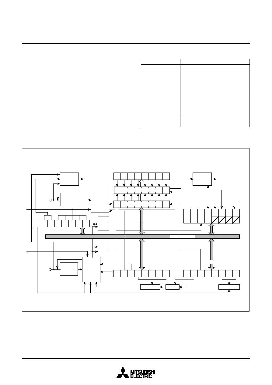
40
3886 Group
SINGLE-CHIP 8-BIT CMOS MICROCOMPUTER
MITSUBISHI MICROCOMPUTERS
Function
In conformity with Philips I
2
C-BUS
standard:
10-bit addressing format
7-bit addressing format
High-speed clock mode
Standard clock mode
In conformity with Philips I
2
C-BUS
standard:
Master transmission
Master reception
Slave transmission
Slave reception
16.1 kHz to 400 kHz (at
= 4 MHz)
20.2 kHz to 312.5 kHz (at
= 5 MHz)
Table 9 Multi-master I
2
C-BUS interface functions
Item
Format
Communication mode
S
CL
clock frequency
System clock
= f(X
IN
)/2 (high-speed mode)
= f(X
IN
)/8 (middle-speed mode)
MULTI-MASTER I
2
C-BUS INTERFACE
The multi-master I
2
C-BUS interface is a serial communications cir-
cuit, conforming to the Philips I
2
C-BUS data transfer format. This
interface, offering both arbitration lost detection and a synchro-
n o u s f u n c t i o n s , i s u s e f u l f o r t h e m u l t i - m a s t e r s e r i a l
communications.
Figure 35 shows a block diagram of the multi-master I
2
C-BUS in-
terface and Table 9 lists the multi-master I
2
C-BUS interface
functions.
This multi-master I
2
C-BUS interface consists of the I
2
C address
register, the I
2
C data shift register, the I
2
C clock control register,
the I
2
C control register, the I
2
C status register, the I
2
C start/stop
condition control register and other control circuits.
When using the multi-master I
2
C-BUS interface, set 1 MHz or
more to
.
Fig. 35 Block diagram of multi-master I
2
C-BUS interface
V
: Purchase of MITSUBISHI ELECTRIC CORPORATIONS I
2
C components conveys a license under the Philips I
2
C Patent Rights to use these components
an I
2
C system, provided that the system conforms to the I
2
C Standard Specification as defined by Philips.
I
2
C
a
d
d
r
e
s
s
r
e
g
i
s
t
e
r
b
7
b
0
S
A
D
6 S
A
D
5 S
A
D
4 S
A
D
3 S
A
D
2 S
A
D
1 S
A
D
0 R
B
W
N
o
i
s
e
e
l
i
m
i
n
a
t
i
o
n
c
i
r
c
u
i
t
S
e
r
i
a
l
d
a
t
a
(
S
D
A
)
A
d
d
r
e
s
s
c
o
m
p
a
r
a
t
o
r
b
7
I
2
C
d
a
t
a
s
h
i
f
t
r
e
g
i
s
t
e
r
b
0
D
a
t
a
c
o
n
t
r
o
l
c
i
r
c
u
i
t
S
y
s
t
e
m
c
l
o
c
k
(
)
I
n
t
e
r
r
u
p
t
g
e
n
e
r
a
t
i
n
g
c
i
r
c
u
i
t
I
n
t
e
r
r
u
p
t
r
e
q
u
e
s
t
s
i
g
n
a
l
(
I
2
C
I
R
Q
)
b
7
M
S
T T
R
X B
B P
I
N
A
L A
A
S A
D
0 L
R
B
b
0
S
1
b
7
b
0
T
I
S
S
1
0
B
I
T
S
A
D
A
L
S
B
C
2
B
C
1 B
C
0
S
1
D
B
i
t
c
o
u
n
t
e
r
B
B
c
i
r
c
u
i
t
C
l
o
c
k
c
o
n
t
r
o
l
c
i
r
c
u
i
t
N
o
i
s
e
e
l
i
m
i
n
a
t
i
o
n
c
i
r
c
u
i
t
S
e
r
i
a
l
c
l
o
c
k
(
S
C
L
)
b
7
b
0
A
C
K
A
C
K
B
I
T
F
A
S
T
M
O
D
E
C
C
R
4 C
C
R
3 C
C
R
2 C
C
R
1 C
C
R
0
I
n
t
e
r
n
a
l
d
a
t
a
b
u
s
C
l
o
c
k
d
i
v
i
s
i
o
n
S
0
S
2
S
0
D
A
L
c
i
r
c
u
i
t
E
S
0
S
I
S
I
2
C
s
t
a
r
t
/
s
t
o
p
c
o
n
d
i
t
i
o
n
c
o
n
t
r
o
l
r
e
g
i
s
t
e
r
S
I
P
S
S
C
4 S
S
C
3 S
S
C
2 S
S
C
1 S
S
C
0
I
2
C
c
l
o
c
k
c
o
n
t
r
o
l
r
e
g
i
s
t
e
r
I
2
C
s
t
a
t
u
s
r
e
g
i
s
t
e
r
S
2
D
I
n
t
e
r
r
u
p
t
g
e
n
e
r
a
t
i
n
g
c
i
r
c
u
i
t
I
n
t
e
r
r
u
p
t
r
e
q
u
e
s
t
s
i
g
n
a
l
(
S
C
L
S
D
A
I
R
Q
)
S
t
o
p
s
e
l
e
c
t
i
o
n
S
T
S
P
S
E
L
C
L
K
S
T
P
I
2
C
c
l
o
c
k
c
o
n
t
r
o
l
r
e
g
i
s
t
e
r

41
3886 Group
SINGLE-CHIP 8-BIT CMOS MICROCOMPUTER
MITSUBISHI MICROCOMPUTERS
[I
2
C Data Shift Register (S0)] 0012
16
The I
2
C data shift register (S0 : address 0012
16
) is an 8-bit shift
register to store receive data and write transmit data.
When transmit data is written into this register, it is transferred to
the outside from bit 7 in synchronization with the S
CL
clock, and
each time one-bit data is output, the data of this register are
shifted by one bit to the left. When data is received, it is input to
this register from bit 0 in synchronization with the S
CL
clock, and
each time one-bit data is input, the data of this register are shifted
by one bit to the left. The minimum 2 cycles of
are required from
the rising of the S
CL
clock until input to this register.
The I
2
C data shift register is in a write enable status only when the
I
2
C-BUS interface enable bit (ES0 bit : bit 3 of address 15
16
) of
the I
2
C control register is "1." The bit counter is reset by a write in-
struction to the I
2
C data shift register. When both the ES0 bit and
the MST bit of the I
2
C status register (address 0014
16
) are "1," the
S
CL
is output by a write instruction to the I
2
C data shift register.
Reading data from the I
2
C data shift register is always enabled re-
gardless of the ES0 bit value.
[I
2
C Address Register (S0D)] 0013
16
The I
2
C address register (address 0013
16
) consists of a 7-bit slave
address and a read/write bit. In the addressing mode, the slave ad-
dress written in this register is compared with the address data to be
received immediately after the START condition is detected.
∑Bit 0: Read/write bit (RBW)
This is not used in the 7-bit addressing mode. In the 10-bit ad-
dressing mode, the first address data to be received is compared
with the contents (SAD6 to SAD0 + RBW) of the I
2
C address reg-
ister.
The RBW bit is cleared to "0" automatically when the stop condi-
tion is detected.
∑Bits 1 to 7: Slave address (SAD0≠SAD6)
These bits store slave addresses. Regardless of the 7-bit address-
ing mode and the 10-bit addressing mode, the address data
transmitted from the master is compared with the contents of
these bits.
Fig. 36 Structure of I
2
C address register
S
A
D
6 S
A
D
5 S
A
D
4 S
A
D
3 S
A
D
2 S
A
D
1 S
A
D
0 R
B
W
S
l
a
v
e
a
d
d
r
e
s
s
I
2
C
a
d
d
r
e
s
s
r
e
g
i
s
t
e
r
(
S
0
D
:
a
d
d
r
e
s
s
0
0
1
3
1
6
)
R
e
a
d
/
w
r
i
t
e
b
i
t
b
7
b0
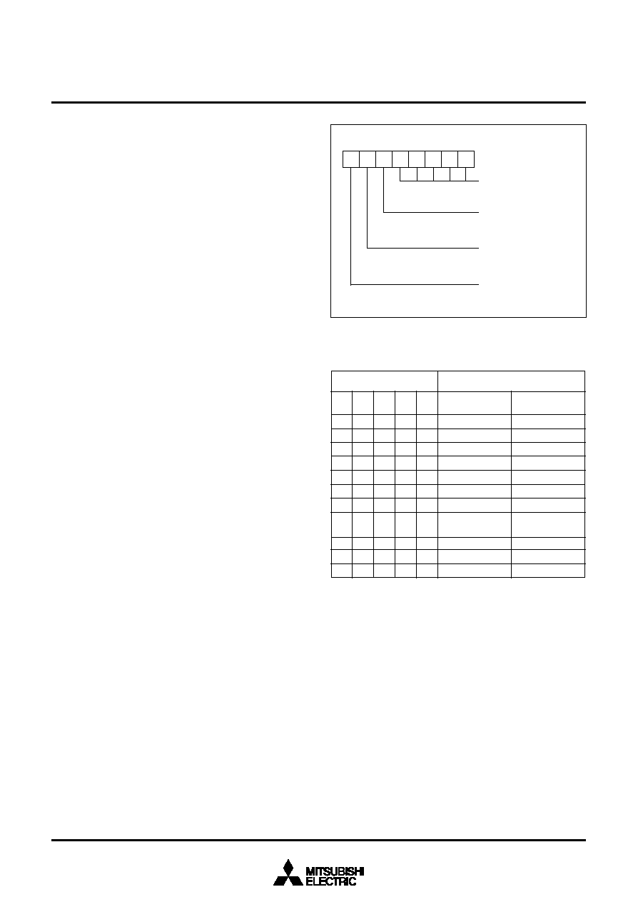
42
3886 Group
SINGLE-CHIP 8-BIT CMOS MICROCOMPUTER
MITSUBISHI MICROCOMPUTERS
Table 10 Set values of I
2
C clock control register and S
CL
frequency
Fig. 37 Structure of I
2
C clock control register
S
CL
frequency
(at
= 4 MHz, unit : kHz) (Note 1)
Setting value of
CCR4≠CCR0
Standard clock
mode
Setting disabled
Setting disabled
Setting disabled
High-speed clock
mode
CCR4
0
0
0
0
0
0
0
1
1
1
CCR3
0
0
0
0
0
0
0
1
1
1
CCR2
0
0
0
0
1
1
1
1
1
1
CCR1
0
0
1
1
0
0
1
0
1
1
CCR0
0
1
0
1
0
1
0
1
0
1
Notes 1: Duty of S
CL
clock output is 50 %. The duty becomes 35 to 45 %
only when the high-speed clock mode is selected and CCR value
= 5 (400 kHz, at
= 4 MHz). "H" duration of the clock fluctuates
from ≠4 to +2 cycles of
in the standard clock mode, and fluctu-
ates from ≠2 to +2 cycles of
in the high-speed clock mode. In
the case of negative fluctuation, the frequency does not increase
because "L" duration is extended instead of "H" duration reduc-
tion.
These are value when S
CL
clock synchronization by the synchro-
nous function is not performed. CCR value is the decimal
notation value of the S
CL
frequency control bits CCR4 to CCR0.
2: Each value of S
CL
frequency exceeds the limit at
= 4 MHz or
more. When using these setting value, use
of 4 MHz or less.
3: The data formula of S
CL
frequency is described below:
/(8
!
CCR value) Standard clock mode
/(4
!
CCR value) High-speed clock mode (CCR value
5)
/(2
!
CCR value) High-speed clock mode (CCR value = 5)
Do not set 0 to 2 as CCR value regardless of
frequency.
Set 100 kHz (max.) in the standard clock mode and 400 kHz
(max.) in the high-speed clock mode to the S
CL
frequency by set-
ting the S
CL
frequency control bits CCR4 to CCR0.
...
...
...
...
...
Setting disabled
Setting disabled
Setting disabled
1000/CCR value
(Note 3)
34.5
33.3
32.3
500/CCR value
(Note 3)
17.2
16.6
16.1
333
250
400 (Note 3)
166
≠ (Note 2)
≠ (Note 2)
100
83.3
[I
2
C Clock Control Register (S2)] 0016
16
The I
2
C clock control register (address 0016
16
) is used to set ACK
control, S
CL
mode and S
CL
frequency.
∑Bits 0 to 4: S
CL
frequency control bits (CCR0≠CCR4)
These bits control the S
CL
frequency. Refer to Table 10.
∑Bit 5: S
CL
mode specification bit (FAST MODE)
This bit specifies the S
CL
mode. When this bit is set to "0," the
standard clock mode is selected. When the bit is set to "1," the
high-speed clock mode is selected.
When connecting the bus of the high-speed mode I
2
C bus stan-
dard (maximum 400 kbits/s), use 8 MHz or more oscillation
frequency f(X
IN
) and high-speed mode (2 division main clock).
∑Bit 6: ACK bit (ACK BIT)
This bit sets the S
DA
status when an ACK clock
V
is generated.
When this bit is set to "0," the ACK return mode is selected and
S
DA
goes to "L" at the occurrence of an ACK clock. When the bit is
set to "1," the ACK non-return mode is selected. The S
DA
is held in
the "H" status at the occurrence of an ACK clock.
However, when the slave address agree with the address data in
the reception of address data at ACK BIT = "0," the S
DA
is auto-
matically made "L" (ACK is returned). If there is a disagreement
between the slave address and the address data, the S
DA
is auto-
matically made "H" (ACK is not returned).
V
ACK clock: Clock for acknowledgment
∑Bit 7: ACK clock bit (ACK)
This bit specifies the mode of acknowledgment which is an ac-
knowledgment response of data transfer. When this bit is set to
"0," the no ACK clock mode is selected. In this case, no ACK clock
occurs after data transmission. When the bit is set to "1," the ACK
clock mode is selected and the master generates an ACK clock
each completion of each 1-byte data transfer. The device for
transmitting address data and control data releases the S
DA
at the
occurrence of an ACK clock (makes S
DA
"H") and receives the
ACK bit generated by the data receiving device.
Note: Do not write data into the I
2
C clock control register during transfer. If
data is written during transfer, the I
2
C clock generator is reset, so
that data cannot be transferred normally.
A
C
K
A
C
K
B
I
T
F
A
S
T
M
O
D
E
C
C
R
4 C
C
R
3 C
C
R
2 C
C
R
1 C
C
R
0
I
2
C
c
l
o
c
k
c
o
n
t
r
o
l
r
e
g
i
s
t
e
r
(
S
2
:
a
d
d
r
e
s
s
0
0
1
6
1
6
)
b
7
b
0
S
C
L
f
r
e
q
u
e
n
c
y
c
o
n
t
r
o
l
b
i
t
s
R
e
f
e
r
t
o
T
a
b
l
e
1
0
.
S
C
L
m
o
d
e
s
p
e
c
i
f
i
c
a
t
i
o
n
b
i
t
0
:
S
t
a
n
d
a
r
d
c
l
o
c
k
m
o
d
e
1
:
H
i
g
h
-
s
p
e
e
d
c
l
o
c
k
m
o
d
e
A
C
K
b
i
t
0
:
A
C
K
i
s
r
e
t
u
r
n
e
d
.
1
:
A
C
K
i
s
n
o
t
r
e
t
u
r
n
e
d
.
A
C
K
c
l
o
c
k
b
i
t
0
:
N
o
A
C
K
c
l
o
c
k
1
:
A
C
K
c
l
o
c
k
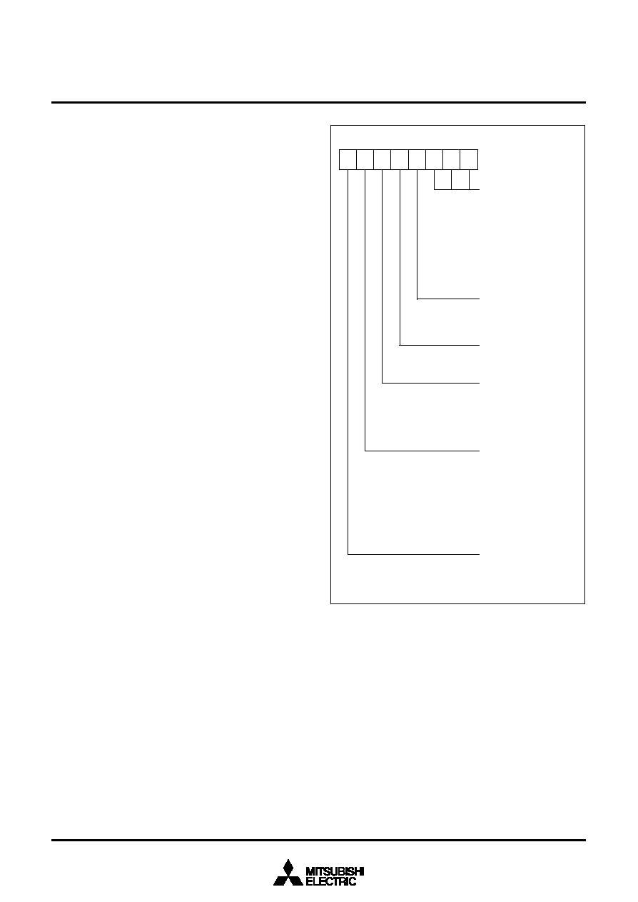
43
3886 Group
SINGLE-CHIP 8-BIT CMOS MICROCOMPUTER
MITSUBISHI MICROCOMPUTERS
Fig. 38 Structure of I
2
C control register
[I
2
C Control Register (S1D)] 0015
16
The I
2
C control register (address 0015
16
) controls data communi-
cation format.
∑Bits 0 to 2: Bit counter (BC0≠BC2)
These bits decide the number of bits for the next 1-byte data to be
transmitted. The I
2
C interrupt request signal occurs immediately
after the number of count specified with these bits (ACK clock is
added to the number of count when ACK clock is selected by ACK
bit (bit 7 of address 0016
16
)) have been transferred, and BC0 to
BC2 are returned to "000
2
".
Also when a START condition is received, these bits become
"000
2
" and the address data is always transmitted and received in
8 bits.
∑Bit 3: I
2
C interface enable bit (ES0)
This bit enables to use the multi-master I
2
C BUS interface. When
this bit is set to "0," the use disable status is provided, so that the
S
DA
and the S
CL
become high-impedance. When the bit is set to
"1," use of the interface is enabled.
When ES0 = "0," the following is performed.
∑ PIN = "1," BB = "0" and AL = "0" are set (which are bits of the I
2
C
status register at address 0014
16
).
∑ Writing data to the I
2
C data shift register (address 0012
16
) is dis
abled.
∑Bit 4: Data format selection bit (ALS)
This bit decides whether or not to recognize slave addresses.
When this bit is set to "0," the addressing format is selected, so
that address data is recognized. When a match is found between
a slave address and address data as a result of comparison or
when a general call (refer to "(5) I
2
C Status Register," bit 1) is re-
ceived, transfer processing can be performed. When this bit is set
to "1," the free data format is selected, so that slave addresses are
not recognized.
∑Bit 5: Addressing format selection bit (10BIT SAD)
This bit selects a slave address specification format. When this bit
is set to "0," the 7-bit addressing format is selected. In this case,
only the high-order 7 bits (slave address) of the I
2
C address regis-
ter (address 0013
16
) are compared with address data. When this
bit is set to "1," the 10-bit addressing format is selected, and all
the bits of the I
2
C address register are compared with address
data.
∑Bit 6: System clock stop selection bit (CLKSTP)
When executing the WIT or STP instruction, this bit selects the
condition of system clock provided to the multi-master I
2
C-BUS in-
terface. When this bit is set to "0," system clock and operation of
the multi-master I
2
C-BUS interface stop by executing the WIT or
STP instruction.
When this bit is set to "1," system clock and operation of the multi-
master I
2
C-BUS interface do not stop even when the WIT
instruction is executed.
When the system clock stop selection bit is "1," do not execute the
STP instruction.
∑Bit 7: I
2
C-BUS interface pin input level selection bit
This bit selects the input level of the S
CL
and S
DA
pins of the multi-
master I
2
C-BUS interface.
b7
T
I
S
S C
L
K
S
T
P
1
0
B
I
T
S
A
D
A
L
S E
S
0 B
C
2 B
C
1 B
C
0
b
0
S
y
s
t
e
m
c
l
o
c
k
s
t
o
p
s
e
l
e
c
t
i
o
n
b
i
t
0
:
S
y
s
t
e
m
c
l
o
c
k
s
t
o
p
w
h
e
n
e
x
e
c
u
t
i
n
g
W
I
T
o
r
S
T
P
i
n
s
t
r
u
c
t
i
o
n
1
:
N
o
t
s
y
s
t
e
m
c
l
o
c
k
s
t
o
p
w
h
e
n
e
x
e
c
u
t
i
n
g
W
I
T
i
n
s
t
r
u
c
t
i
o
n
(
D
o
n
o
t
u
s
e
t
h
e
S
T
P
i
n
s
t
r
u
c
t
i
o
n
.
)
I
2
C
c
o
n
t
r
o
l
r
e
g
i
s
t
e
r
(
S
1
D
:
a
d
d
r
e
s
s
0
0
1
5
1
6
)
B
i
t
c
o
u
n
t
e
r
(
N
u
m
b
e
r
o
f
t
r
a
n
s
m
i
t
/
r
e
c
e
i
v
e
b
i
t
s
)
b
2 b
1 b
0
0
0
0 :
8
0
0
1 :
7
0
1
0 :
6
0
1
1 :
5
1
0
0 :
4
1
0
1 :
3
1
1
0 :
2
1
1
1 :
1
I
2
C
-
B
U
S
i
n
t
e
r
f
a
c
e
e
n
a
b
l
e
b
i
t
0
:
D
i
s
a
b
l
e
d
1
:
E
n
a
b
l
e
d
D
a
t
a
f
o
r
m
a
t
s
e
l
e
c
t
i
o
n
b
i
t
0
:
A
d
d
r
e
s
s
i
n
g
f
o
r
m
a
t
1
:
F
r
e
e
d
a
t
a
f
o
r
m
a
t
A
d
d
r
e
s
s
i
n
g
f
o
r
m
a
t
s
e
l
e
c
t
i
o
n
b
i
t
0
:
7
-
b
i
t
a
d
d
r
e
s
s
i
n
g
f
o
r
m
a
t
1
:
1
0
-
b
i
t
a
d
d
r
e
s
s
i
n
g
f
o
r
m
a
t
I
2
C
-
B
U
S
i
n
t
e
r
f
a
c
e
p
i
n
i
n
p
u
t
l
e
v
e
l
s
e
l
e
c
t
i
o
n
b
i
t
0
:
C
M
O
S
i
n
p
u
t
1
:
S
M
B
U
S
i
n
p
u
t

44
3886 Group
SINGLE-CHIP 8-BIT CMOS MICROCOMPUTER
MITSUBISHI MICROCOMPUTERS
∑Bit 4: I
2
C-BUS interface interrupt request bit (PIN)
This bit generates an interrupt request signal. Each time 1-byte
data is transmitted, the PIN bit changes from "1" to "0." At the
same time, an interrupt request signal occurs to the CPU. The PIN
bit is set to "0" in synchronization with a falling of the last clock (in-
cluding the ACK clock) of an internal clock and an interrupt
request signal occurs in synchronization with a falling of the PIN
bit. When the PIN bit is "0," the S
CL
is kept in the "0" state and
clock generation is disabled. Figure 40 shows an interrupt request
signal generating timing chart.
The PIN bit is set to "1" in one of the following conditions:
∑ Executing a write instruction to the I
2
C data shift register (ad-
dress 0012
16
). (This is the only condition which the prohibition of
the internal clock is released and data can be communicated ex-
cept for the start condition detection.)
∑ When the ES0 bit is "0"
∑ At reset
∑ When writing "1" to the PIN bit by software
The conditions in which the PIN bit is set to "0" are shown below:
∑ Immediately after completion of 1-byte data transmission (includ-
ing when arbitration lost is detected)
∑ Immediately after completion of 1-byte data reception
∑ In the slave reception mode, with ALS = "0" and immediately af-
ter completion of slave address agreement or general call
address reception
∑ In the slave reception mode, with ALS = "1" and immediately af-
ter completion of address data reception
∑Bit 5: Bus busy flag (BB)
This bit indicates the status of use of the bus system. When this
bit is set to "0," this bus system is not busy and a START condition
can be generated. The BB flag is set/reset by the S
CL
, S
DA
pins in-
put signal regardless of master/slave. This flag is set to "1" by
detecting the start condition, and is set to "0" by detecting the stop
condition. The condition of these detecting is set by the start/stop
condition setting bits (SSC4≠SSC0) of the I
2
C start/stop condition
control register (address 0017
16
). When the ES0 bit (bit 3) of the
I
2
C control register (address 0015
16
) is "0" or reset, the BB flag is
set to "0."
For the writing function to the BB flag, refer to the sections
"START Condition Generating Method" and "STOP Condition Gen-
erating Method" described later.
[I
2
C Status Register (S1)] 0014
16
The I
2
C status register (address 0014
16
) controls the I
2
C-BUS in-
terface status. The low-order 4 bits are read-only bits and the
high-order 4 bits can be read out and written to.
Set "0000
2
" to the low-order 4 bits, because these bits become the
reserved bits at writing.
∑Bit 0: Last receive bit (LRB)
This bit stores the last bit value of received data and can also be
used for ACK receive confirmation. If ACK is returned when an
ACK clock occurs, the LRB bit is set to "0." If ACK is not returned,
this bit is set to "1." Except in the ACK mode, the last bit value of
received data is input. The state of this bit is changed from "1" to
"0" by executing a write instruction to the I
2
C data shift register
(address 0012
16
).
∑Bit 1: General call detecting flag (AD0)
When the ALS bit is "0," this bit is set to "1" when a general call
V
whose address data is all "0" is received in the slave mode. By a
general call of the master device, every slave device receives con-
trol data after the general call. The AD0 bit is set to "0" by
detecting the STOP condition or START condition, or reset.
V
General call: The master transmits the general call address "00
16
" to all
slaves.
∑Bit 2: Slave address comparison flag (AAS)
This flag indicates a comparison result of address data when the
ALS bit is "0".
In the slave receive mode, when the 7-bit addressing format is
selected, this bit is set to "1" in one of the following conditions:
∑
The address data immediately after occurrence of a START
condition agrees with the slave address stored in the high-or-
der 7 bits of the I
2
C address register (address 0013
16
).
∑
A general call is received.
In the slave reception mode, when the 10-bit addressing format
is selected, this bit is set to "1" with the following condition:
∑
When the address data is compared with the I
2
C address reg-
ister (8 bits consisting of slave address and RBW bit), the first
bytes agree.
This bit is set to "0" by executing a write instruction to the I
2
C
data shift register (address 0012
16
) when ES0 is set to "1" or
reset.
∑Bit 3: Arbitration lost
V
detecting flag (AL)
In the master transmission mode, when the SDA is made "L" by
any other device, arbitration is judged to have been lost, so that
this bit is set to "1." At the same time, the TRX bit is set to "0," so
that immediately after transmission of the byte whose arbitration
was lost is completed, the MST bit is set to "0." The arbitration lost
can be detected only in the master transmission mode. When ar-
bitration is lost during slave address transmission, the TRX bit is
set to "0" and the reception mode is set. Consequently, it becomes
possible to detect the agreement of its own slave address and ad-
dress data transmitted by another master device.
V
Arbitration lost :The status in which communication as a master is dis-
abled.
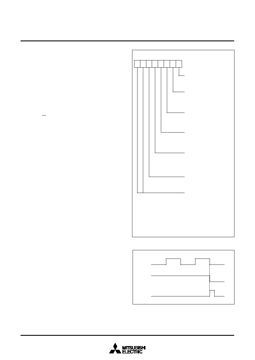
45
3886 Group
SINGLE-CHIP 8-BIT CMOS MICROCOMPUTER
MITSUBISHI MICROCOMPUTERS
Fig. 40 Interrupt request signal generating timing
Fig. 39 Structure of I
2
C status register
∑Bit 6: Communication mode specification bit (transfer direc-
tion specification bit: TRX)
This bit decides a direction of transfer for data communication.
When this bit is "0," the reception mode is selected and the data of
a transmitting device is received. When the bit is "1," the transmis-
sion mode is selected and address data and control data are
output onto the S
DA
in synchronization with the clock generated on
the S
CL
.
This bit is set/reset by software and hardware. About set/reset by
hardware is described below. This bit is set to "1" by hardware
when all the following conditions are satisfied:
∑ When ALS is "0"
∑ In the slave reception mode or the slave transmission mode
∑ When the R/W bit reception is "1"
This bit is set to "0" in one of the following conditions:
∑ When arbitration lost is detected.
∑ When a STOP condition is detected.
∑ When writing "1" to this bit by software is invalid by the START
condition duplication preventing function (Note).
∑ With MST = "0" and when a START condition is detected.
∑ With MST = "0" and when ACK non-return is detected.
∑ At reset
∑Bit 7: Communication mode specification bit (master/slave
specification bit: MST)
This bit is used for master/slave specification for data communica-
tion. When this bit is "0," the slave is specified, so that a START
condition and a STOP condition generated by the master are re-
ceived, and data communication is performed in synchronization
with the clock generated by the master. When this bit is "1," the
master is specified and a START condition and a STOP condition
are generated. Additionally, the clocks required for data communi-
cation are generated on the SCL.
This bit is set to "0" in one of the following conditions.
∑ Immediately after completion of 1-byte data transfer when arbi-
tration lost is detected
∑ When a STOP condition is detected.
∑ Writing "1" to this bit by software is invalid by the START condi-
tion duplication preventing function (Note).
∑ At reset
Note: START condition duplication preventing function
The MST, TRX, and BB bits is set to "1" at the same time after con-
firming that the BB flag is "0" in the procedure of a START condition
occurrence. However, when a START condition by another master
device occurs and the BB flag is set to "1" immediately after the con-
tents of the BB flag is confirmed, the START condition duplication
preventing function makes the writing to the MST and TRX bits in-
valid. The duplication preventing function becomes valid from the
rising of the BB flag to reception completion of slave address.
b
7
M
S
T
b
0
I
2
C
s
t
a
t
u
s
r
e
g
i
s
t
e
r
(
S
1
:
a
d
d
r
e
s
s
0
0
1
4
1
6
)
L
a
s
t
r
e
c
e
i
v
e
b
i
t
(
N
o
t
e
)
0
: L
a
s
t
b
i
t
=
"
0
"
1
: L
a
s
t
b
i
t
=
"
1
"
G
e
n
e
r
a
l
c
a
l
l
d
e
t
e
c
t
i
n
g
f
l
a
g
(
N
o
t
e
)
0
: N
o
g
e
n
e
r
a
l
c
a
l
l
d
e
t
e
c
t
e
d
1
: G
e
n
e
r
a
l
c
a
l
l
d
e
t
e
c
t
e
d
S
l
a
v
e
a
d
d
r
e
s
s
c
o
m
p
a
r
i
s
o
n
f
l
a
g
(
N
o
t
e
)
0
:
A
d
d
r
e
s
s
d
i
s
a
g
r
e
e
m
e
n
t
1
:
A
d
d
r
e
s
s
a
g
r
e
e
m
e
n
t
A
r
b
i
t
r
a
t
i
o
n
l
o
s
t
d
e
t
e
c
t
i
n
g
f
l
a
g
(
N
o
t
e
)
0
: N
o
t
d
e
t
e
c
t
e
d
1
: D
e
t
e
c
t
e
d
I
2
C
-
B
U
S
i
n
t
e
r
f
a
c
e
i
n
t
e
r
r
u
p
t
r
e
q
u
e
s
t
b
i
t
0
:
I
n
t
e
r
r
u
p
t
r
e
q
u
e
s
t
i
s
s
u
e
d
1
:
N
o
i
n
t
e
r
r
u
p
t
r
e
q
u
e
s
t
i
s
s
u
e
d
B
u
s
b
u
s
y
f
l
a
g
0
:
B
u
s
f
r
e
e
1
:
B
u
s
b
u
s
y
C
o
m
m
u
n
i
c
a
t
i
o
n
m
o
d
e
s
p
e
c
i
f
i
c
a
t
i
o
n
b
i
t
s
0
0
: S
l
a
v
e
r
e
c
e
i
v
e
m
o
d
e
0
1
: S
l
a
v
e
t
r
a
n
s
m
i
t
m
o
d
e
1
0
: M
a
s
t
e
r
r
e
c
e
i
v
e
m
o
d
e
1
1
: M
a
s
t
e
r
t
r
a
n
s
m
i
t
m
o
d
e
T
R
X B
B P
I
N A
L A
A
S A
D
0 L
R
B
N
o
t
e
:
T
h
e
s
e
b
i
t
a
n
d
f
l
a
g
s
c
a
n
b
e
r
e
a
d
o
u
t
b
u
t
c
a
n
n
o
t
b
e
w
r
i
t
t
e
n
.
W
r
i
t
e
"
0
"
t
o
t
h
e
s
e
b
i
t
s
a
t
w
r
i
t
i
n
g
.
S
C
L
P
I
N
I
2
C
I
R
Q
46
3886 Group
SINGLE-CHIP 8-BIT CMOS MICROCOMPUTER
MITSUBISHI MICROCOMPUTERS
+ 2 cycles (3.375
µ
s)
+ 1 cycle < 4.0
µ
s (3.25
µ
s)
Fig. 43 START condition detecting timing diagram
START/STOP Condition Detecting Operation
The START/STOP condition detection operations are shown in
Figures 43, 44, and Table 13. The START/STOP condition is set
by the START/STOP condition set bit.
The START/STOP condition can be detected only when the input
signal of the S
CL
and S
DA
pins satisfy three conditions: S
CL
re-
lease time, setup time, and hold time (see Table 13).
The BB flag is set to "1" by detecting the START condition and is
reset to "0" by detecting the STOP condition.
The BB flag set/reset timing is different in the standard clock mode
and the high-speed clock mode. Refer to Table 13, the BB flag set/
reset time.
Note: When a STOP condition is detected in the slave mode (MST = 0), an
interrupt request signal "I
2
CIRQ" occurs to the CPU.
Table 13 START condition/STOP condition detecting conditions
Note: Unit : Cycle number of system clock
SSC value is the decimal notation value of the START/STOP condi-
tion set bits SSC4 to SSC0. Do not set "0" or an odd number to SSC
value. The value in parentheses is an example when the I
2
C START/
STOP condition control register is set to "18
16
" at
= 4 MHz.
Fig. 44 STOP condition detecting timing diagram
S
CL
release time
Standard clock mode
High-speed clock mode
4 cycles (1.0
µ
s)
2 cycles (1.0
µ
s)
2 cycles (0.5
µ
s)
3.5 cycles (0.875
µ
s)
SSC value
2
SSC value
2
SSC value ≠1
2
Setup time
Hold time
BB flag set/
reset time
SSC value + 1 cycle (6.25
µ
s)
cycle < 4.0
µ
s (3.0
µ
s)
START Condition Generating Method
When writing "1" to the MST, TRX, and BB bits of the I
2
C status
register (address 0014
16
) at the same time after writing the slave
address to the I
2
C data shift register (address 0012
16
) with the
condition in which the ES0 bit of the I
2
C control register (address
0015
16
) and the BB flag are "0", a START condition occurs. After
that, the bit counter becomes "000
2
" and an S
CL
for 1 byte is out-
put. The START condition generating timing is different in the
standard clock mode and the high-speed clock mode. Refer to
Figure 41, the START condition generating timing diagram, and
Table 11, the START condition generating timing table.
STOP Condition Generating Method
When the ES0 bit of the I
2
C control register (address 0015
16
) is
"1," write "1" to the MST and TRX bits, and write "0" to the BB bit
of the I
2
C status register (address 0014
16
) simultaneously. Then a
STOP condition occurs. The STOP condition generating timing is
different in the standard clock mode and the high-speed clock
mode. Refer to Figure 42, the STOP condition generating timing
diagram, and Table 12, the STOP condition generating timing
table.
Fig. 41 START condition generating timing diagram
Fig. 42 STOP condition generating timing diagram
Table 12 STOP condition generating timing table
Item
Setup
time
START/STOP condition
generating selection bit
"0"
"1"
"0"
"1"
Standard
clock mode
5.5
µ
s (22 cycles)
13.5
µ
s (54 cycles)
5.5
µ
s (22 cycles)
13.5
µ
s (54 cycles)
Note: Absolute time at
= 4 MHz. The value in parentheses denotes the
number of
cycles.
High-speed
clock mode
3.0
µ
s (12 cycles)
7.0
µ
s (28 cycles)
3.0
µ
s (12 cycles)
7.0
µ
s (28 cycles)
Table 11 START condition generating timing table
Item
Setup
time
START/STOP condition
generating selection bit
Standard
clock mode
Note: Absolute time at
= 4 MHz. The value in parentheses denotes the
number of
cycles.
High-speed
clock mode
"0"
"1"
"0"
"1"
5.0
µ
s (20 cycles)
13.0
µ
s (52 cycles)
5.0
µ
s (20 cycles)
13.0
µ
s (52 cycles)
2.5
µ
s (10 cycles)
6.5
µ
s (26 cycles)
2.5
µ
s (10 cycles)
6.5
µ
s (26 cycles)
Hold
time
Hold
time
I
2
C
s
t
a
t
u
s
r
e
g
i
s
t
e
r
w
r
i
t
e
s
i
g
n
a
l
H
o
l
d
t
i
m
e
S
e
t
u
p
t
i
m
e
S
C
L
S
D
A
I
2
C
s
t
a
t
u
s
r
e
g
i
s
t
e
r
w
r
i
t
e
s
i
g
n
a
l
H
o
l
d
t
i
m
e
S
e
t
u
p
t
i
m
e
S
C
L
S
D
A
H
o
l
d
t
i
m
e
S
e
t
u
p
t
i
m
e
S
C
L
S
D
A
B
B
f
l
a
g
S
C
L
r
e
l
e
a
s
e
t
i
m
e
B
B
f
l
a
g
r
e
s
e
t
t
i
m
e
H
o
l
d
t
i
m
e
S
e
t
u
p
t
i
m
e
S
C
L
S
D
A
B
B
f
l
a
g
S
C
L
r
e
l
e
a
s
e
t
i
m
e
B
B
f
l
a
g
r
e
s
e
t
t
i
m
e

47
3886 Group
SINGLE-CHIP 8-BIT CMOS MICROCOMPUTER
MITSUBISHI MICROCOMPUTERS
[I
2
C START/STOP Condition Control Register
(S2D)] 0017
16
The I
2
C START/STOP condition control register (address 0017
16
)
controls START/STOP condition detection.
∑Bits 0 to 4: START/STOP condition set bit (SSC4≠SSC0)
S
CL
release time, setup time, and hold time change the detection
condition by value of the main clock divide ratio selection bit and
the oscillation frequency f(X
IN
) because these time are measured
by the internal system clock. Accordingly, set the proper value to
the START/STOP condition set bits (SSC4 to SSC0) in considered
of the system clock frequency. Refer to Table 13.
Do not set "00000
2
" or an odd number to the START/STOP condi-
tion set bit (SSC4 to SSC0).
Refer to Table 14, the recommended set value to START/STOP
condition set bits (SSC4≠SSC0) for each oscillation frequency.
∑Bit 5: S
CL
/S
DA
interrupt pin polarity selection bit (SIP)
An interrupt can occur when detecting the falling or rising edge of
the S
CL
or S
DA
pin. This bit selects the polarity of the S
CL
or S
DA
pin interrupt pin.
∑Bit 6: S
CL
/S
DA
interrupt pin selection bit (SIS)
This bit selects the pin of which interrupt becomes valid between
the S
CL
pin and the S
DA
pin.
Note: When changing the setting of the S
CL
/S
DA
interrupt pin polarity se-
lection bit, the S
CL
/S
DA
interrupt pin selection bit, or the I
2
C-BUS
interface enable bit ES0, the S
CL
/S
DA
interrupt request bit may be
set. When selecting the S
CL
/S
DA
interrupt source, disable the inter-
rupt before the S
CL
/S
DA
interrupt pin polarity selection bit, the S
CL
/
S
DA
interrupt pin selection bit, or the I
2
C-BUS interface enable bit
ES0 is set. Reset the request bit to "0" after setting these bits, and
enable the interrupt.
∑Bit 7: START/STOP condition generating selection bit
(STSPSEL)
Setup/Hold time when the START/STOP condition is generated
can be selected.
Cycle number of system clock becomes standard for setup/hold
time. Additionally, setup/hold time is different between the START
condition and the STP condition. (Refer to Tables 11 and 12.) Set
"1" to this bit when the system clock frequency is 4 MHz or more.
Address Data Communication
There are two address data communication formats, namely, 7-bit
addressing format and 10-bit addressing format. The respective
address communication formats are described below.
7-bit addressing format
To adapt the 7-bit addressing format, set the 10BIT SAD bit of
the I
2
C control register (address 0015
16
) to "0." The first 7-bit
address data transmitted from the master is compared with the
high-order 7-bit slave address stored in the I
2
C address register
(address 0013
16
). At the time of this comparison, address com-
parison of the RBW bit of the I
2
C address register (address
0013
16
) is not performed. For the data transmission format
when the 7-bit addressing format is selected, refer to Figure 46,
(1) and (2).
10-bit addressing format
To adapt the 10-bit addressing format, set the 10BIT SAD bit of
the I
2
C control register (address 0015
16
) to "1." An address
comparison is performed between the first-byte address data
transmitted from the master and the 8-bit slave address stored
in the I
2
C address register (address 0013
16
). At the time of this
comparison, an address comparison between the RBW bit of
the I
2
C address register (address 0013
16
) and the R/W bit
which is the last bit of the address data transmitted from the
master is made. In the 10-bit addressing mode, the RBW bit
which is the last bit of the address data not only specifies the
direction of communication for control data, but also is pro-
cessed as an address data bit.
When the first-byte address data agree with the slave address,
the AAS bit of the I
2
C status register (address 0014
16
) is set to
"1." After the second-byte address data is stored into the I
2
C
data shift register (address 0012
16
), perform an address com-
parison between the second-byte data and the slave address
by software. When the address data of the 2 bytes agree with
the slave address, set the RBW bit of the I
2
C address register
(address 0013
16
) to "1" by software. This processing can make
the 7-bit slave address and R/W data agree, which are re-
ceived after a RESTART condition is detected, with the value of
the I
2
C address register (address 0013
16
). For the data trans-
mission format when the 10-bit addressing format is selected,
refer to Figure 46, (3) and (4).
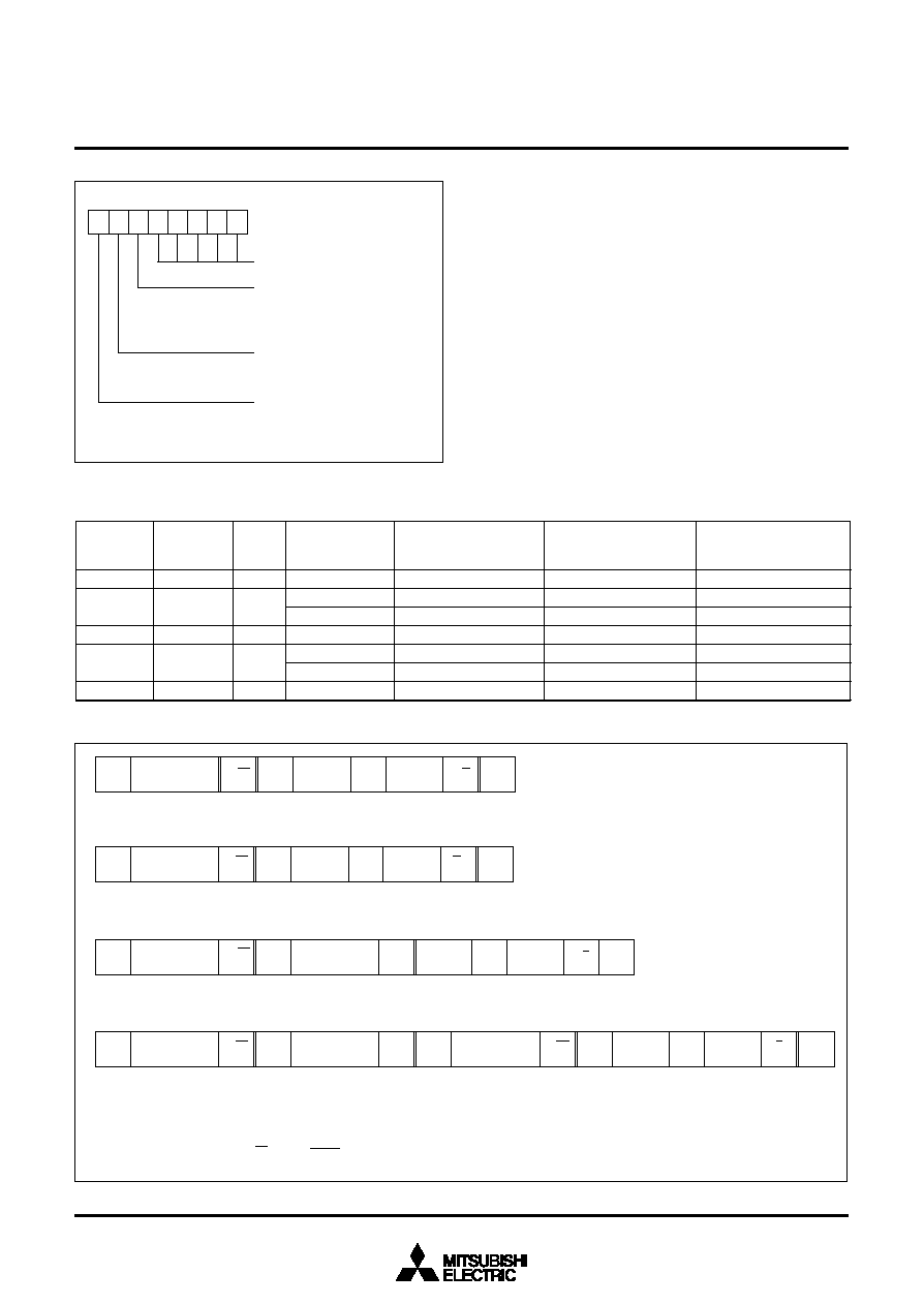
48
3886 Group
SINGLE-CHIP 8-BIT CMOS MICROCOMPUTER
MITSUBISHI MICROCOMPUTERS
START/STOP
condition
control register
Oscillation
frequency
f(X
IN
) (MHz)
Fig. 46 Address data communication format
Fig. 45 Structure of I
2
C START/STOP condition control register
Note: Do not set "00000
2
" or an odd number to the START/STOP condition set bit (SSC4 to SSC0).
Table 14 Recommended set value to START/STOP condition set bits (SSC4≠SSC0) for each oscillation frequency
Main clock
divide ratio
System
clock
(MHz)
S
CL
release time
(
µ
s)
Setup time
(
µ
s)
Hold time
(
µ
s)
10
8
8
4
2
2
2
8
2
2
XXX11110
XXX11010
XXX11000
XXX00100
XXX01100
XXX01010
XXX00100
3.2
µ
s (16 cycles)
3.5
µ
s (14 cycles)
3.25
µ
s (13 cycles)
3.0
µ
s (3 cycles)
3.5
µ
s (7 cycles)
3.0
µ
s (6 cycles)
3.0
µ
s (3 cycles)
6.2
µ
s (31 cycles)
6.75
µ
s (27 cycles)
6.25
µ
s (25 cycles)
5.0
µ
s (5 cycles)
6.5
µ
s (13 cycles)
5.5
µ
s (11 cycles)
5.0
µ
s (5 cycles)
3.0
µ
s (15 cycles)
3.25
µ
s (13 cycles)
3.0
µ
s (12 cycles)
2.0
µ
s (2 cycles)
3.0
µ
s (6 cycles)
2.5
µ
s (5 cycles)
2.0
µ
s (2 cycles)
5
4
1
2
1
b
7
S
T
S
P
S
E
L
b
0
I
2
C
S
T
A
R
T
/
S
T
O
P
c
o
n
d
i
t
i
o
n
c
o
n
t
r
o
l
r
e
g
i
s
t
e
r
S
T
A
R
T
/
S
T
O
P
c
o
n
d
i
t
i
o
n
s
e
t
b
i
t
S
C
L
/
S
D
A
i
n
t
e
r
r
u
p
t
p
i
n
p
o
l
a
r
i
t
y
s
e
l
e
c
t
i
o
n
b
i
t
0
: F
a
l
l
i
n
g
e
d
g
e
a
c
t
i
v
e
1
: R
i
s
i
n
g
e
d
g
e
a
c
t
i
v
e
S
C
L
/
S
D
A
i
n
t
e
r
r
u
p
t
p
i
n
s
e
l
e
c
t
i
o
n
b
i
t
0
: S
D
A
v
a
l
i
d
1
: S
C
L
v
a
l
i
d
S
T
A
R
T
/
S
T
O
P
c
o
n
d
i
t
i
o
n
g
e
n
e
r
a
t
i
n
g
s
e
l
e
c
t
i
o
n
b
i
t
0
: S
e
t
u
p
/
H
o
l
d
t
i
m
e
s
h
o
r
t
m
o
d
e
1
: S
e
t
u
p
/
H
o
l
d
t
i
m
e
l
o
n
g
m
o
d
e
S
I
S S
I
P
S
S
C
4 S
S
C
3 S
S
C
2 S
S
C
1 S
S
C
0
(
S
2
D
:
a
d
d
r
e
s
s
0
0
1
7
1
6
)
S
S
l
a
v
e
a
d
d
r
e
s
s
R
/
W
A
D
a
t
a
A
D
a
t
a
A
/
A
P
7
b
i
t
s
"
0
"
1
t
o
8
b
i
t
s
1
t
o
8
b
i
t
s
(
1
)
A
m
a
s
t
e
r
-
t
r
a
n
s
m
i
t
t
e
r
t
r
a
n
s
n
m
i
t
s
d
a
t
a
t
o
a
s
l
a
v
e
-
r
e
c
e
i
v
e
r
S
S
l
a
v
e
a
d
d
r
e
s
s R
/
W
A
D
a
t
a
A
D
a
t
a
A
P
7
b
i
t
s
"
1
"
1
t
o
8
b
i
t
s
1
t
o
8
b
i
t
s
(
2
)
A
m
a
s
t
e
r
-
r
e
c
e
i
v
e
r
r
e
c
e
i
v
e
s
d
a
t
a
f
r
o
m
a
s
l
a
v
e
-
t
r
a
n
s
m
i
t
t
e
r
S
S
l
a
v
e
a
d
d
r
e
s
s
1
s
t
7
b
i
t
s
R
/
W
A
7
b
i
t
s
"
0
"
8
b
i
t
s
(
3
)
A
m
a
s
t
e
r
-
t
r
a
n
s
m
i
t
t
e
r
t
r
a
n
s
m
i
t
s
d
a
t
a
t
o
a
s
l
a
v
e
-
r
e
c
e
i
v
e
r
w
i
t
h
a
1
0
-
b
i
t
a
d
d
r
e
s
s
S
l
a
v
e
a
d
d
r
e
s
s
2
n
d
b
y
t
e
s
A
D
a
t
a
A
D
a
t
a
A
/
A
P
1
t
o
8
b
i
t
s
1
t
o
8
b
i
t
s
S
S
l
a
v
e
a
d
d
r
e
s
s
1
s
t
7
b
i
t
s
R
/
W
A
7
b
i
t
s
"
0
"
8
b
i
t
s
(
4
)
A
m
a
s
t
e
r
-
r
e
c
e
i
v
e
r
r
e
c
e
i
v
e
s
d
a
t
a
f
r
o
m
a
s
l
a
v
e
-
t
r
a
n
s
m
i
t
t
e
r
w
i
t
h
a
1
0
-
b
i
t
a
d
d
r
e
s
s
S
l
a
v
e
a
d
d
r
e
s
s
2
n
d
b
y
t
e
s
A
D
a
t
a
A
A
S
r
S
l
a
v
e
a
d
d
r
e
s
s
1
s
t
7
b
i
t
s
R
/
W
A
D
a
t
a
P
S
:
S
T
A
R
T
c
o
n
d
i
t
i
o
n
A
:
A
C
K
b
i
t
S
r
:
R
e
s
t
a
r
t
c
o
n
d
i
t
i
o
n
P
:
S
T
O
P
c
o
n
d
i
t
i
o
n
R
/
W
:
R
e
a
d
/
W
r
i
t
e
b
i
t
7
b
i
t
s
"
1
"
1
t
o
8
b
i
t
s
1
t
o
8
b
i
t
s

49
3886 Group
SINGLE-CHIP 8-BIT CMOS MICROCOMPUTER
MITSUBISHI MICROCOMPUTERS
Example of Master Transmission
An example of master transmission in the standard clock mode, at
the S
CL
frequency of 100 kHz and in the ACK return mode is
shown below.
Set a slave address in the high-order 7 bits of the I
2
C address
register (address 0013
16
) and "0" into the RBW bit.
Set the ACK return mode and S
CL
= 100 kHz by setting "85
16
" in
the I
2
C clock control register (address 0016
16
).
Set "00
16
" in the I
2
C status register (address 0014
16
) so that
transmission/reception mode can become initializing condition.
Set a communication enable status by setting "08
16
" in the I
2
C
control register (address 0015
16
).
Confirm the bus free condition by the BB flag of the I
2
C status
register (address 0014
16
).
Set the address data of the destination of transmission in the
high-order 7 bits of the I
2
C data shift register (address 0012
16
)
and set "0" in the least significant bit.
Set "F0
16
" in the I
2
C status register (address 0014
16
) to gener-
ate a START condition. At this time, an S
CL
for 1 byte and an
ACK clock automatically occur.
Set transmit data in the I
2
C data shift register (address 0012
16
).
At this time, an S
CL
and an ACK clock automatically occur.
When transmitting control data of more than 1 byte, repeat step
.
Set "D0
16
" in the I
2
C status register (address 0014
16
) to gener-
ate a STOP condition if ACK is not returned from slave
reception side or transmission ends.
Example of Slave Reception
An example of slave reception in the high-speed clock mode, at
the S
CL
frequency of 400 kHz, in the ACK non-return mode and
using the addressing format is shown below.
Set a slave address in the high-order 7 bits of the I
2
C address
register (address 0013
16
) and "0" in the RBW bit.
Set the no ACK clock mode and S
CL
= 400 kHz by setting "25
16
"
in the I
2
C clock control register (address 0016
16
).
Set "00
16
" in the I
2
C status register (address 0014
16
) so that
transmission/reception mode can become initializing condition.
Set a communication enable status by setting "08
16
" in the I
2
C
control register (address 0015
16
).
When a START condition is received, an address comparison is
performed.
∑When all transmitted addresses are "0" (general call):
AD0 of the I
2
C status register (address 0014
16
) is set to "1"
and an interrupt request signal occurs.
∑ When the transmitted addresses agree with the address set
in
:
ASS of the I
2
C status register (address 0014
16
) is set to "1"
and an interrupt request signal occurs.
∑ In the cases other than the above AD0 and AAS of the I
2
C sta-
tus register (address 0014
16
) are set to "0" and no interrupt
request signal occurs.
Set dummy data in the I
2
C data shift register (address 0012
16
).
When receiving control data of more than 1 byte, repeat step
.
When a STOP condition is detected, the communication ends.
s
Precautions when using multi-master I
2
C-
BUS interface
(1) Read-modify-write instruction
The precautions when the read-modify-write instruction such as
SEB, CLB etc. is executed for each register of the multi-master
I
2
C-BUS interface are described below.
∑ I
2
C data shift register (S0: address 0012
16
)
When executing the read-modify-write instruction for this regis-
ter during transfer, data may become a value not intended.
∑ I
2
C address register (S0D: address 0013
16
)
When the read-modify-write instruction is executed for this regis-
ter at detecting the STOP condition, data may become a value
not intended. It is because H/W changes the read/write bit
(RBW) at the above timing.
∑ I
2
C status register (S1: address 0014
16
)
Do not execute the read-modify-write instruction for this register
because all bits of this register are changed by H/W.
∑ I
2
C control register (S1D: address 0015
16
)
When the read-modify-write instruction is executed for this regis-
ter at detecting the START condition or at completing the byte
transfer, data may become a value not intended. Because H/W
changes the bit counter (BC0-BC2) at the above timing.
∑ I
2
C clock control register (S2: address 0016
16
)
The read-modify-write instruction can be executed for this regis-
ter.
∑ I
2
C START/STOP condition control register (S2D: address
0017
16
)
The read-modify-write instruction can be executed for this regis-
ter.

50
3886 Group
SINGLE-CHIP 8-BIT CMOS MICROCOMPUTER
MITSUBISHI MICROCOMPUTERS
.....
.....
.....
.....
.....
(2) START condition generating procedure using multi-master
1. Procedure example (The necessary conditions of the generat-
ing procedure are described as the following 2 to 5.
LDA --
(Taking out of slave address value)
SEI
(Interrupt disabled)
BBS 5, S1, BUSBUSY (BB flag confirming and branch pro-
cess)
BUSFREE:
STA S0
(Writing of slave address value)
LDM #$F0, S1
(Trigger of START condition generating)
CLI
(Interrupt enabled)
BUSBUSY:
CLI
(Interrupt enabled)
2. Use "Branch on Bit Set" of "BBS 5, $0014, ≠" for the BB flag
confirming and branch process.
3. Use "STA $12, STX $12" or "STY $12" of the zero page ad-
dressing instruction for writing the slave address value to the
I
2
C data shift register.
4. Execute the branch instruction of above 2 and the store instruc-
tion of above 3 continuously shown the above procedure
example.
5. Disable interrupts during the following three process steps:
∑ BB flag confirming
∑ Writing of slave address value
∑ Trigger of START condition generating
When the condition of the BB flag is bus busy, enable interrupts
immediately.
(3) RESTART condition generating procedure
This cannot be applied when the external memory is used and the
bus cycle is extended by ONW function.
1. Procedure example (The necessary conditions of the generat-
ing procedure are described as the following 2 to 4.)
Execute the following procedure when the PIN bit is "0."
LDM #$00, S1
(Select slave receive mode)
LDA --
(Taking out of slave address value)
SEI
(Interrupt disabled)
STA S0
(Writing of slave address value)
LDM #$F0, S1
(Trigger of RESTART condition generating)
CLI
(Interrupt enabled)
2. Select the slave receive mode when the PIN bit is "0." Do not
write "1" to the PIN bit. Neither "0" nor "1" is specified for the
writing to the BB bit.
The TRX bit becomes "0" and the S
DA
pin is released.
3. The S
CL
pin is released by writing the slave address value to
the I
2
C data shift register.
4. Disable interrupts during the following two process steps:
∑ Writing of slave address value
∑ Trigger of RESTART condition generating
(4) Writing to I
2
C status register
Do not execute an instruction to set the PIN bit to "1" from "0" and
an instruction to set the MST and TRX bits to "0" from "1" simulta-
neously. It is because it may enter the state that the S
CL
pin is
released and the S
DA
pin is released after about one machine
cycle. Do not execute an instruction to set the MST and TRX bits
to "0" from "1" simultaneously when the PIN bit is "1." It is because
it may become the same as above.
(5) Process of after STOP condition generating
Do not write data in the I
2
C data shift register S0 and the I
2
C sta-
tus register S1 until the bus busy flag BB becomes "0" after
generating the STOP condition in the master mode. It is because
the STOP condition waveform might not be normally generated.
Reading to the above registers do not have the problem.
(6) STOP condition input at 7th clock pulse
In the slave mode, the STOP condition is input at the 7th clock
pulse while receiving a slave address or data. As the clock pulse
is continuously input, the SDA line may be held at LOW even if
flag BB is set to "0" (only for M38867M8A and M38867E8).
Countermeasure:
Write dummy data to the I
2
C shift register or reset the ES0 bit in
the S1D register (ES0 = "L"
ES0 = "H") during a stop condition
interrupt routine with flag PIN = "1".
Note: Do not use the read-modify-write instruction at this time.
Furthermore, when the ES0 bit is set to "0", it becomes a
general-purpose port; so that the port must be set to input
mode or "H".
(7) ES0 bit switch
In standard clock mode when SSC = "00010
2
" or in high-speed
clock mode, flag BB may switch to "1" if ES0 bit is set to "1" when
SDA is "L".
Countermeasure:
Set ES0 to "1" when SDA is "H".
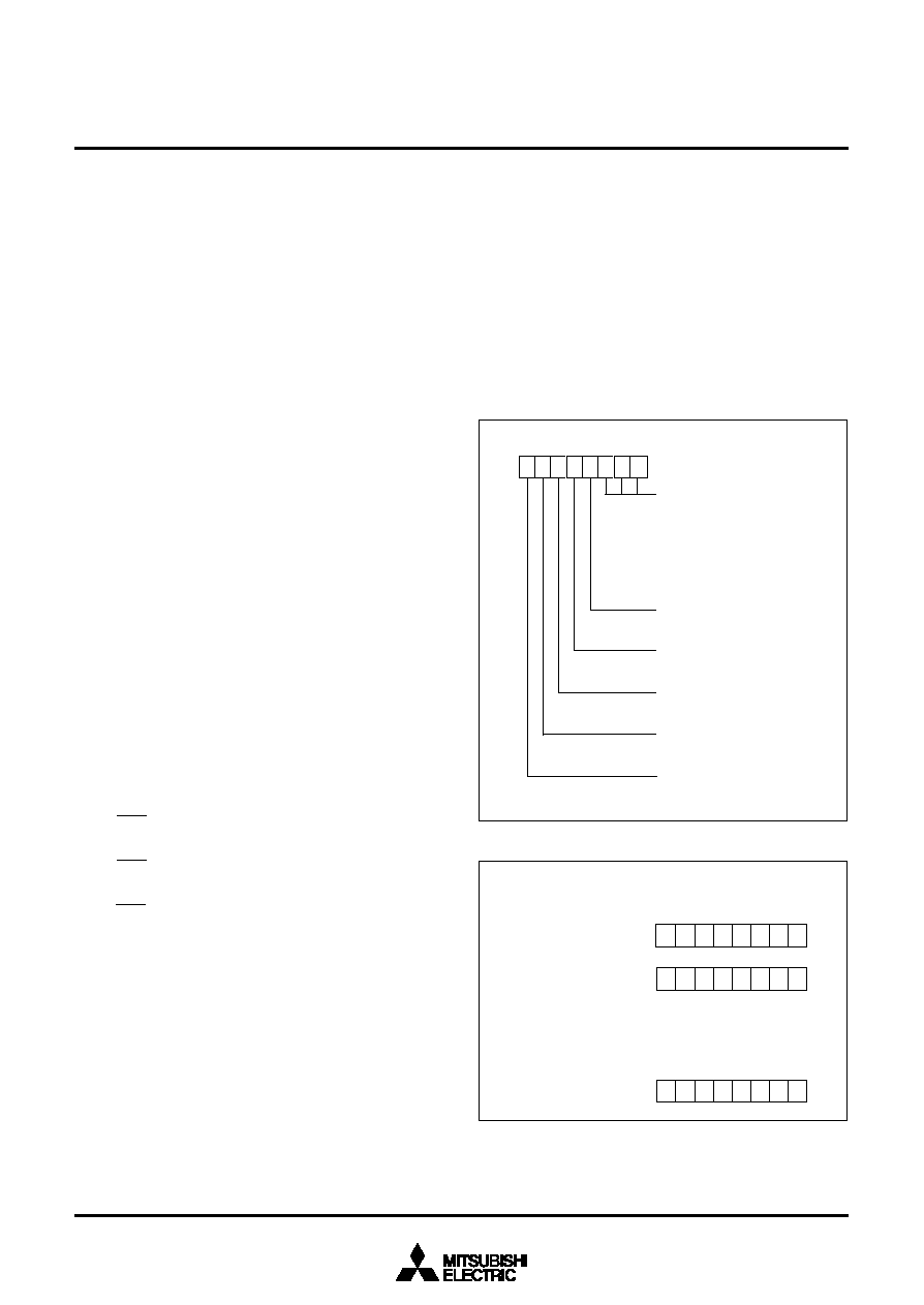
51
3886 Group
SINGLE-CHIP 8-BIT CMOS MICROCOMPUTER
MITSUBISHI MICROCOMPUTERS
A-D CONVERTER
[A-D Conversion Register 1,2 (AD1, AD2)]
0035
16
, 0038
16
The A-D conversion register is a read-only register that stores the
result of an A-D conversion. When reading this register during an
A-D conversion, the previous conversion result is read.
Bit 7 of the A-D conversion register 2 is the conversion mode se-
lection bit. When this bit is set to "0," the A-D converter becomes
the 10-bit A-D mode. When this bit is set to "1," that becomes the
8-bit A-D mode. The conversion result of the 8-bit A-D mode is
stored in the A-D conversion register 1. As for 10-bit A-D mode,
10-bit reading or 8-bit reading can be performed by selecting the
reading procedure of the A-D conversion register 1, 2 after A-D
conversion is completed (in Figure 48).
The A-D conversion register 1 performs the 8-bit reading inclined
to MSB after reset, the A-D conversion is started, or reading of the
A-D converter register 1 is generated; and the register becomes
the 8-bit reading inclined to LSB after the A-D converter register 2
is generated.
[AD/DA Control Register (ADCON)] 0034
16
The AD/DA control register controls the A-D conversion process.
Bits 0 to 2 select a specific analog input pin. Bit 3 signals the
completion of an A-D conversion. The value of this bit remains at
"0" during an A-D conversion, and changes to "1" when an A-D
conversion ends. Writing "0" to this bit starts the A-D conversion.
Comparison Voltage Generator
The comparison voltage generator divides the voltage between
AV
SS
and V
REF
into 1024, and outputs the divided voltages in the
10-bit A-D mode (256 division in 8-bit A-D mode).
The A-D converter successively compares the comparison voltage
V
ref
in each mode, dividing the V
REF
(see below), with the input
voltage.
∑ 10-bit A-D mode (10-bit reading)
V
ref
=
!
n (n = 0≠1023)
∑ 10-bit A-D mode (8-bit reading)
V
ref
=
!
n (n = 0≠255)
∑ 8-bit A-D mode
V
ref
=
!
(n≠0.5) (n = 1≠255)
=0
(n = 0)
Fig. 47 Structure of AD/DA control register
Channel Selector
The channel selector selects one of ports P6
0
/AN
0
to P6
7
/AN
7
,
and inputs the voltage to the comparator.
Comparator and Control Circuit
The comparator and control circuit compares an analog input volt-
age with the comparison voltage, and then stores the result in the
A-D conversion registers 1, 2. When an A-D conversion is com-
pleted, the control circuit sets the A-D conversion completion bit
and the A-D interrupt request bit to "1".
Note that because the comparator consists of a capacitor cou-
pling, set f(X
IN
) to 500 kHz or more during an A-D conversion.
V
REF
256
V
REF
256
Fig. 48 Structure of 10-bit A-D mode reading
V
REF
1024
A
D
/
D
A
c
o
n
t
r
o
l
r
e
g
i
s
t
e
r
(
A
D
C
O
N
:
a
d
d
r
e
s
s
0
0
3
4
1
6
)
A
n
a
l
o
g
i
n
p
u
t
p
i
n
s
e
l
e
c
t
i
o
n
b
i
t
s
0
0
0
:
P
6
0
/
A
N
0
0
0
1
:
P
6
1
/
A
N
1
0
1
0
:
P
6
2
/
A
N
2
0
1
1
:
P
6
3
/
A
N
3
1
0
0
:
P
6
4
/
A
N
4
1
0
1
:
P
6
5
/
A
N
5
1
1
0
:
P
6
6
/
A
N
6
1
1
1
:
P
6
7
/
A
N
7
A
-
D
c
o
n
v
e
r
s
i
o
n
c
o
m
p
l
e
t
i
o
n
b
i
t
0
:
C
o
n
v
e
r
s
i
o
n
i
n
p
r
o
g
r
e
s
s
1
:
C
o
n
v
e
r
s
i
o
n
c
o
m
p
l
e
t
e
d
P
W
M
0
o
u
t
p
u
t
p
i
n
s
e
l
e
c
t
i
o
n
b
i
t
0
:
P
5
6
/
P
W
M
0
1
1
:
P
3
0
/
P
W
M
0
0
P
W
M
1
o
u
t
p
u
t
p
i
n
s
e
l
e
c
t
i
o
n
b
i
t
0
:
P
5
7
/
P
W
M
1
1
1
:
P
3
1
/
P
W
M
1
0
D
A
1
o
u
t
p
u
t
e
n
a
b
l
e
b
i
t
0
:
D
A
1
o
u
t
p
u
t
d
i
s
a
b
l
e
d
1
:
D
A
1
o
u
t
p
u
t
e
n
a
b
l
e
d
D
A
2
o
u
t
p
u
t
e
n
a
b
l
e
b
i
t
0
:
D
A
2
o
u
t
p
u
t
d
i
s
a
b
l
e
d
1
:
D
A
2
o
u
t
p
u
t
e
n
a
b
l
e
d
b
7
b
0
b
2
b
1
b
0
1
0
-
b
i
t
r
e
a
d
i
n
g
(
R
e
a
d
a
d
d
r
e
s
s
0
0
3
8
1
6
b
e
f
o
r
e
0
0
3
5
1
6
)
(
A
d
d
r
e
s
s
0
0
3
8
1
6
)
(
A
d
d
r
e
s
s
0
0
3
5
1
6
)
8
-
b
i
t
r
e
a
d
i
n
g
(
R
e
a
d
o
n
l
y
a
d
d
r
e
s
s
0
0
3
5
1
6
)
(
A
d
d
r
e
s
s
0
0
3
5
1
6
)
b
8
b
7 b
6 b
5 b
4 b
3 b
2 b
1 b
0
b
7
b
0
b
9
b
7
b
0
N
o
t
e
:
B
i
t
s
2
t
o
6
o
f
a
d
d
r
e
s
s
0
0
3
8
1
6
b
e
c
o
m
e
s
"
0
"
a
t
r
e
a
d
i
n
g
.
b
9 b
8 b
7 b
6 b
5 b
4 b
3 b
2
b
7
b
0
0
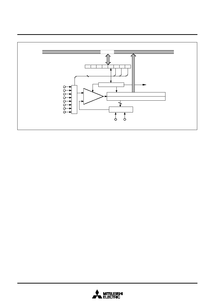
52
3886 Group
SINGLE-CHIP 8-BIT CMOS MICROCOMPUTER
MITSUBISHI MICROCOMPUTERS
Fig. 49 Block diagram of A-D converter
C
h
a
n
n
e
l
s
e
l
e
c
t
o
r
A
-
D
c
o
n
t
r
o
l
c
i
r
c
u
i
t
A
-
D
c
o
n
v
e
r
s
i
o
n
r
e
g
i
s
t
e
r
1
R
e
s
i
s
t
o
r
l
a
d
d
e
r
V
R
E
F
A
V
S
S
C
o
m
p
a
r
a
t
o
r
A
-
D
i
n
t
e
r
r
u
p
t
r
e
q
u
e
s
t
b
7
b
0
3
1
0
P
6
0
/
A
N
0
P
6
1
/
A
N
1
P
6
2
/
A
N
2
P
6
3
/
A
N
3
P
6
4
/
A
N
4
P
6
5
/
A
N
5
P
6
6
/
A
N
6
P
6
7
/
A
N
7
D
a
t
a
b
u
s
A
D
/
D
A
c
o
n
t
r
o
l
r
e
g
i
s
t
e
r
A
-
D
c
o
n
v
e
r
s
i
o
n
r
e
g
i
s
t
e
r
2
(
A
d
d
r
e
s
s
0
0
3
4
1
6
)
(
A
d
d
r
e
s
s
0
0
3
8
1
6
)
(
A
d
d
r
e
s
s
0
0
3
5
1
6
)
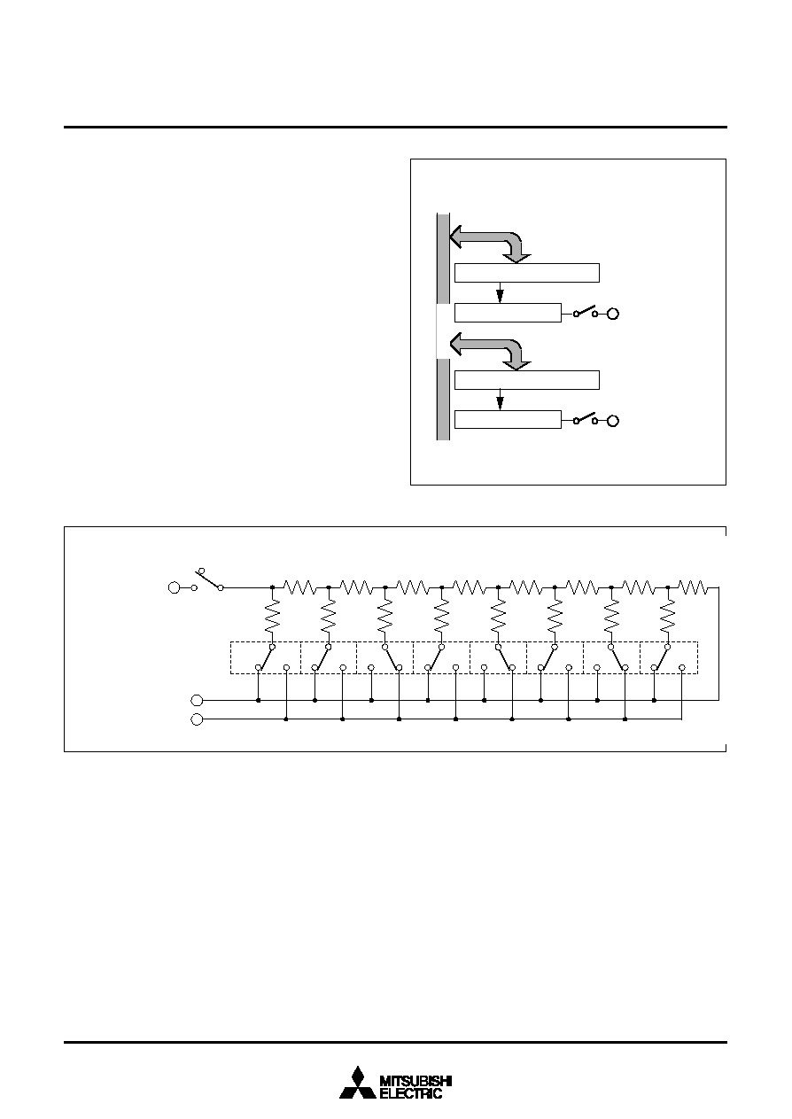
53
3886 Group
SINGLE-CHIP 8-BIT CMOS MICROCOMPUTER
MITSUBISHI MICROCOMPUTERS
D-A CONVERTER
The 3886 group has two internal D-A converters (DA
1
and DA
2
)
with 8-bit resolution.
The D-A converter is performed by setting the value in each D-A
conversion register. The result of D-A conversion is output from
the DA
1
or DA
2
pin by setting the DA output enable bit to "1".
When using the D-A converter, the corresponding port direction
register bit (P5
6
/DA
1
/PWM
01
or P5
7
/DA
2
/PWM
11
) must be set to
"0" (input status).
The output analog voltage V is determined by the value n (decimal
notation) in the D-A conversion register as follows:
V = V
REF
!
n/256 (n = 0 to 255)
Where V
REF
is the reference voltage.
At reset, the D-A conversion registers are cleared to "00
16
", the
DA output enable bits are cleared to "0", and the P5
6
/DA
1
/PWM
01
and P5
7
/DA
2
/PWM
11
pins become high impedance.
The DA output does not have buffers. Accordingly, connect an ex-
ternal buffer when driving a low-impedance load.
Set V
CC
to 4.0 V or more when using the D-A converter.
Fig. 50 Block diagram of D-A converter
Fig. 51 Equivalent connection circuit of D-A converter (DA1)
P
5
6
/
D
A
1
/
P
W
M
0
1
D
-
A
1
c
o
n
v
e
r
s
i
o
n
r
e
g
i
s
t
e
r
(
8
)
R
-
2
R
r
e
s
i
s
t
o
r
l
a
d
d
e
r
D
A
1
o
u
t
p
u
t
e
n
a
b
l
e
b
i
t
P
5
7
/
D
A
2
/
P
W
M
1
1
D
-
A
2
c
o
n
v
e
r
s
i
o
n
r
e
g
i
s
t
e
r
(
8
)
R
-
2
R
r
e
s
i
s
t
o
r
l
a
d
d
e
r
D
A
2
o
u
t
p
u
t
e
n
a
b
l
e
b
i
t
D
a
t
a
b
u
s
A
V
S
S
V
R
E
F
"
0
"
"
1
"
M
S
B
"
0
"
"
1
"
R
2
R
R
2
R
R
2
R
R
2
R
R
2
R
R
2
R
R
2
R
2
R
L
S
B
2
R
P
5
6
/
D
A
1
/
P
W
M
0
1
D
-
A
1
c
o
n
v
e
r
s
i
o
n
r
e
g
i
s
t
e
r
D
A
1
o
u
t
p
u
t
e
n
a
b
l
e
b
i
t
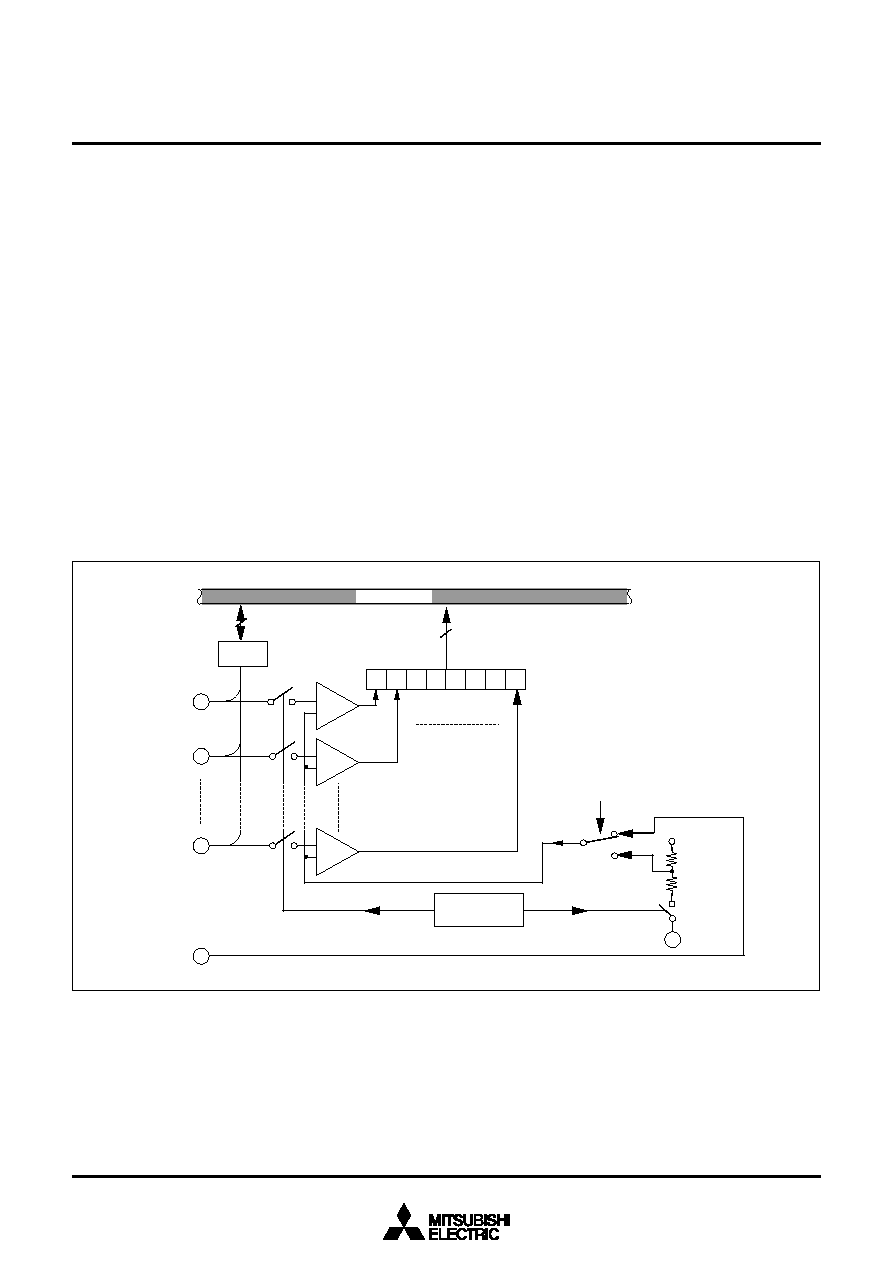
54
3886 Group
SINGLE-CHIP 8-BIT CMOS MICROCOMPUTER
MITSUBISHI MICROCOMPUTERS
COMPARATOR CIRCUIT
Comparator Configuration
The comparator circuit consists of resistors, comparators, a com-
parator control circuit, the comparator reference input selection bit
(bit 7 of address 001D
16
), a comparator data register (address
002D
16
), the comparator reference power source input pin (P0
0
/
P3
REF
) and analog signal input pins (P3
0
≠P3
7
). The analog input
pin (P3
0
≠P3
7
) also functions as an ordinary digital port.
Comparator Operation
To activate the comparator, first set port P3 to input mode by set-
ting the corresponding direction register (address 0007
16
) to "0" to
use port P3 as an analog voltage input pin. The internal fixed ana-
log voltage (V
CC
!
29/32) can be generated by setting "1" to the
comparator reference input selection bit (bit 7) of the serial I/O2
control register (address 001D
16
). (The internal fixed analog volt-
age becomes about 4.5 V at V
CC
= 5.0 V.) When setting "0" to the
comparator reference input selection bit, the P0
0
/P3
REF
pin be-
comes the comparator reference power source input pin and it is
possible to input the comparator reference power source option-
ally from the external. The voltage comparison is immediately
performed by the writing operation to the comparator data register
(address 002D
16
). After 14 cycles of the internal system clock
(the time required for the comparison), the comparison result is
stored in the comparator register (address 002D
16
).
If the analog input voltage is greater than the internal reference
voltage, each bit of this register is "1"; if it is less than the internal
reference voltage, each bit of this register is "0". To perform an-
other comparison, the voltage comparison must be performed
again by writing to the comparator data register (address 002D
16
).
Read the result when 14 cycles of
or more have passed after the
comparator operation starts. The ladder resistor is turned on dur-
ing 14 cycles of
, which is required for the comparison, and the
reference voltage is generated. An unnecessary current is not
consumed because the ladder resistor is turned off while the com-
parator operation is not performed. Since the comparator consists
of capacitor coupling, the electric charge is lost if the clock fre-
quency is low.
Keep that the clock frequency is 1 MHz or more during the com-
parator operation. Do not execute the STP, WIT, or port P3 I/O
instruction.
Fig. 52 Comparator circuit
V
S
S
8
8
V
C
C
P
3
(
8
)
P
3
7
P
3
6
P
3
0
b
0
C
o
m
p
a
r
a
t
o
r
r
e
f
e
r
e
n
c
e
i
n
p
u
t
s
e
l
e
c
t
i
o
n
b
i
t
(
b
i
t
7
)
o
f
s
e
r
i
a
l
I
/
O
2
c
o
n
t
r
o
l
r
e
g
i
s
t
e
r
(
a
d
d
r
e
s
s
0
0
1
D
1
6
)
C
o
m
p
a
r
a
t
o
r
d
a
t
a
r
e
g
i
s
t
e
r
(
a
d
d
r
e
s
s
0
0
2
D
1
6
)
C
o
m
p
a
r
-
a
t
o
r
L
a
d
d
e
r
r
e
s
i
s
t
o
r
c
o
n
n
e
c
t
i
n
g
s
i
g
n
a
l
C
o
m
p
a
r
a
t
o
r
c
o
n
t
r
o
l
c
i
r
c
u
i
t
C
o
m
p
a
r
a
t
o
r
c
o
n
n
e
c
t
i
n
g
s
i
g
n
a
l
C
o
m
p
a
r
-
a
t
o
r
C
o
m
p
a
r
-
a
t
o
r
P
0
0
/
P
3
R
E
F
V
C
C
!
2
9
/
3
2
"
1
"
"
0
"
D
a
t
a
b
u
s
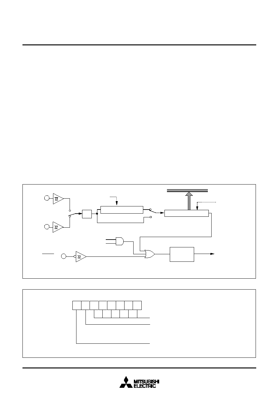
55
3886 Group
SINGLE-CHIP 8-BIT CMOS MICROCOMPUTER
MITSUBISHI MICROCOMPUTERS
WATCHDOG TIMER
The watchdog timer gives a mean of returning to the reset status
when a program cannot run on a normal loop (for example, be-
cause of a software run-away). The watchdog timer consists of an
8-bit watchdog timer L and an 8-bit watchdog timer H.
Standard Operation of Watchdog Timer
When any data is not written into the watchdog timer control reg-
ister (address 001E
16
) after resetting, the watchdog timer is in the
stop state. The watchdog timer starts to count down by writing an
optional value into the watchdog timer control register (address
001E
16
) and an internal reset occurs at an underflow of the watch-
dog timer H.
Accordingly, programming is usually performed so that writing to
the watchdog timer control register (address 001E
16
) may be
started before an underflow. When the watchdog timer control reg-
ister (address 001E
16
) is read, the values of the high-order 6 bits
of the watchdog timer H, STP instruction disable bit, and watch-
dog timer H count source selection bit are read.
Initial Value of Watchdog Timer
At reset or writing to the watchdog timer control register (address
001E
16
), each watchdog timer H and L is set to "FF
16
."
Fig. 54 Structure of Watchdog timer control register
q
Watchdog timer H count source selection bit operation
Bit 7 of the watchdog timer control register (address 001E
16
) per-
mits selecting a watchdog timer H count source. When this bit is
set to "0", the count source becomes the underflow signal of
watchdog timer L. The detection time is set to f(X
IN
)=131.072 ms
at 8 MHz frequency and f(X
CIN
)=32.768 s at 32 kHz frequency.
When this bit is set to "1", the count source becomes the signal
divided by 16 for f(X
IN
) (or f(X
CIN
)). The detection time in this case
is set to f(X
IN
)= 512
µ
s at 8 MHz frequency and f(X
CIN
)=128 ms at
32 kHz frequency. This bit is cleared to "0" after resetting.
q
Operation of STP instruction disable bit
Bit 6 of the watchdog timer control register (address 001E
16
) per-
mits disabling the STP instruction when the watchdog timer is in
operation.
When this bit is "0", the STP instruction is enabled.
When this bit is "1", the STP instruction is disabled.
Once the STP instruction is executed, an internal reset occurs.
When this bit is set to "1", it cannot be rewritten to "0" by program.
This bit is cleared to "0" after resetting.
Fig. 53 Block diagram of Watchdog timer
X
IN
Data bus
X
CIN
"10"
"00"
"01"
Main clock division
ratio selection bits
(Note)
"0"
"1"
1/16
Watchdog timer H count
source selection bit
Reset
circuit
STP instruction disable bit
Watchdog timer H (8)
"FF
16
" is set when
watchdog timer
control register is
written to.
Internal reset
RESET
Watchdog timer L (8)
Note: Either high-speed, middle-speed or low-speed mode is selected by bits 7 and 6 of the CPU mode register.
STP instruction
"FF
16
" is set when
watchdog timer
control register is
written to.
b
0
S
T
P
i
n
s
t
r
u
c
t
i
o
n
d
i
s
a
b
l
e
b
i
t
0
:
S
T
P
i
n
s
t
r
u
c
t
i
o
n
e
n
a
b
l
e
d
1
:
S
T
P
i
n
s
t
r
u
c
t
i
o
n
d
i
s
a
b
l
e
d
W
a
t
c
h
d
o
g
t
i
m
e
r
H
c
o
u
n
t
s
o
u
r
c
e
s
e
l
e
c
t
i
o
n
b
i
t
0
:
W
a
t
c
h
d
o
g
t
i
m
e
r
L
u
n
d
e
r
f
l
o
w
1
:
f
(
X
I
N
)
/
1
6
o
r
f
(
X
C
I
N
)
/
1
6
W
a
t
c
h
d
o
g
t
i
m
e
r
H
(
f
o
r
r
e
a
d
-
o
u
t
o
f
h
i
g
h
-
o
r
d
e
r
6
b
i
t
)
W
a
t
c
h
d
o
g
t
i
m
e
r
c
o
n
t
r
o
l
r
e
g
i
s
t
e
r
(
W
D
T
C
O
N
:
a
d
d
r
e
s
s
0
0
1
E
1
6
)
b
7
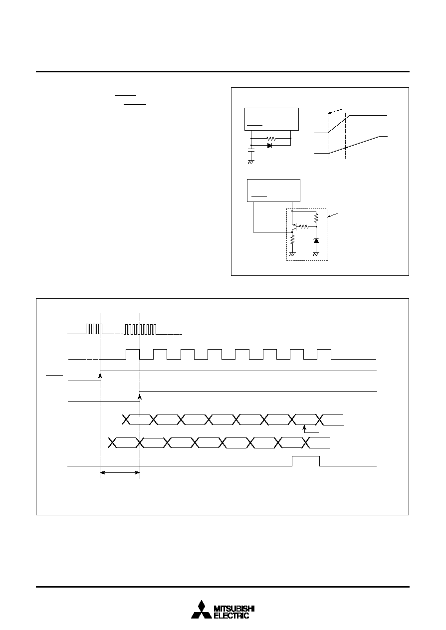
56
3886 Group
SINGLE-CHIP 8-BIT CMOS MICROCOMPUTER
MITSUBISHI MICROCOMPUTERS
RESET CIRCUIT
To reset the microcomputer, RESET pin should be held at an "L"
level for 2
µ
s or more. Then the RESET pin is returned to an "H"
level (the power source voltage should be between 2.7 V and 5.5
V (4.0 V to 5.5 V for flash memory version), and the oscillation
should be stable), reset is released. After the reset is completed,
the program starts from the address contained in address FFFD
16
(high-order byte) and address FFFC
16
(low-order byte). Make sure
that the reset input voltage is less than 0.54 V for V
CC
of 2.7 V. For
flash memory version, make sure that the reset input voltage is
less than 0.8 V for Vcc of 4.0 V.
Fig. 56 Reset sequence
Fig. 55 Reset circuit example
(Note)
0.2V
CC
0V
0V
Poweron
V
CC
RESET
V
CC
RESET
Power source
voltage detection
circuit
Power source
voltage
Reset input
voltage
Note : Reset release voltage ; Vcc=2.7 V
(Vcc = 4.0 V for flash memory version)
R
E
S
E
T
I
n
t
e
r
n
a
l
r
e
s
e
t
D
a
t
a
A
d
d
r
e
s
s
S
Y
N
C
X
I
N
:
1
0
.
5
t
o
1
8
.
5
c
l
o
c
k
c
y
c
l
e
s
X
I
N
?
?
?
?
?
F
F
F
C
F
F
F
D
A
D
H
,
L
?
?
?
?
?
A
D
L
A
D
H
1
:
T
h
e
f
r
e
q
u
e
n
c
y
r
e
l
a
t
i
o
n
o
f
f
(
X
I
N
)
a
n
d
f
(
)
i
s
f
(
X
I
N
)
=
8
∑
f
(
)
.
2
:
T
h
e
q
u
e
s
t
i
o
n
m
a
r
k
s
(
?
)
i
n
d
i
c
a
t
e
a
n
u
n
d
e
f
i
n
e
d
s
t
a
t
e
t
h
a
t
d
e
p
e
n
d
s
o
n
t
h
e
p
r
e
v
i
o
u
s
s
t
a
t
e
.
R
e
s
e
t
a
d
d
r
e
s
s
f
r
o
m
t
h
e
v
e
c
t
o
r
t
a
b
l
e
.
N
o
t
e
s
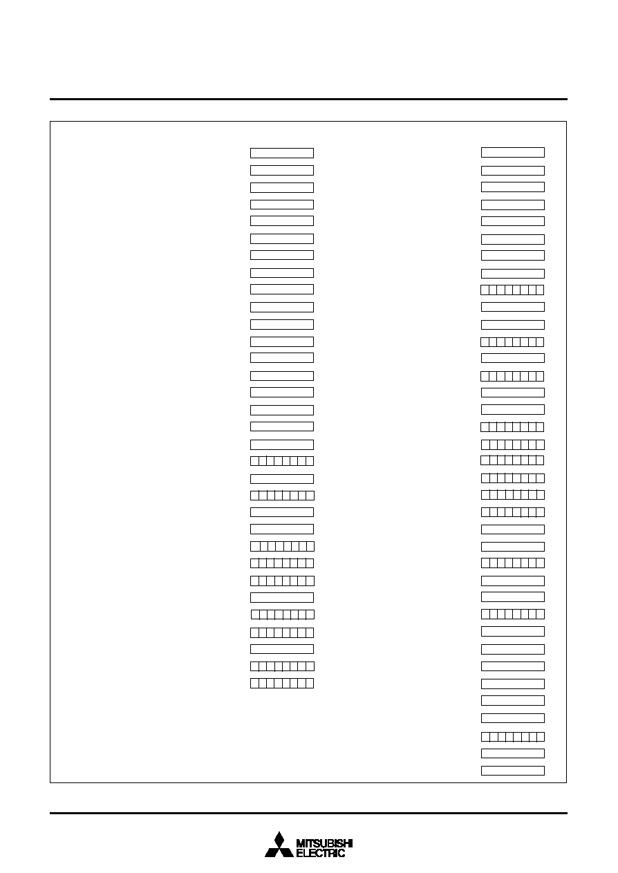
57
3886 Group
SINGLE-CHIP 8-BIT CMOS MICROCOMPUTER
MITSUBISHI MICROCOMPUTERS
Fig. 57 Internal status at reset
P
o
r
t
P
0
(
P
0
)
P
o
r
t
P
0
d
i
r
e
c
t
i
o
n
r
e
g
i
s
t
e
r
(
P
0
D
)
P
o
r
t
P
1
(
P
1
)
P
o
r
t
P
1
d
i
r
e
c
t
i
o
n
r
e
g
i
s
t
e
r
(
P
1
D
)
P
o
r
t
P
2
(
P
2
)
P
o
r
t
P
2
d
i
r
e
c
t
i
o
n
r
e
g
i
s
t
e
r
(
P
2
D
)
P
o
r
t
P
3
(
P
3
)
P
o
r
t
P
3
d
i
r
e
c
t
i
o
n
r
e
g
i
s
t
e
r
(
P
3
D
)
P
o
r
t
P
4
(
P
4
)
P
o
r
t
P
4
d
i
r
e
c
t
i
o
n
r
e
g
i
s
t
e
r
(
P
4
D
)
P
o
r
t
P
5
(
P
5
)
P
o
r
t
P
5
d
i
r
e
c
t
i
o
n
r
e
g
i
s
t
e
r
(
P
5
D
)
P
o
r
t
P
6
(
P
6
)
P
o
r
t
P
6
d
i
r
e
c
t
i
o
n
r
e
g
i
s
t
e
r
(
P
6
D
)
P
o
r
t
P
7
(
P
7
)
P
o
r
t
P
7
d
i
r
e
c
t
i
o
n
r
e
g
i
s
t
e
r
(
P
7
D
)
P
o
r
t
P
8
(
P
8
)
P
o
r
t
P
8
d
i
r
e
c
t
i
o
n
r
e
g
i
s
t
e
r
(
P
8
D
)
I
2
C
d
a
t
a
s
h
i
f
t
r
e
g
i
s
t
e
r
(
S
0
)
I
2
C
a
d
d
r
e
s
s
r
e
g
i
s
t
e
r
(
S
0
D
)
I
2
C
s
t
a
t
u
s
r
e
g
i
s
t
e
r
(
S
1
)
I
2
C
c
o
n
t
r
o
l
r
e
g
i
s
t
e
r
(
S
1
D
)
I
2
C
c
l
o
c
k
c
o
n
t
r
o
l
r
e
g
i
s
t
e
r
(
S
2
)
I2C
s
t
a
r
t
/
s
t
o
p
c
o
n
d
i
t
i
o
n
c
o
n
t
r
o
l
r
e
g
i
s
t
e
r
(
S
2
D
)
T
r
a
n
s
m
i
t
/
R
e
c
e
i
v
e
b
u
f
f
e
r
r
e
g
i
s
t
e
r
(
T
B
/
R
B
)
S
e
r
i
a
l
I
/
O
1
s
t
a
t
u
s
r
e
g
i
s
t
e
r
(
S
I
O
1
S
T
S
)
S
e
r
i
a
l
I
/
O
1
c
o
n
t
r
o
l
r
e
g
i
s
t
e
r
(
S
I
O
1
C
O
N
)
U
A
R
T
c
o
n
t
r
o
l
r
e
g
i
s
t
e
r
(
U
A
R
T
C
O
N
)
B
a
u
d
r
a
t
e
g
e
n
e
r
a
t
o
r
(
B
R
G
)
S
e
r
i
a
l
I
/
O
2
c
o
n
t
r
o
l
r
e
g
i
s
t
e
r
(
S
I
O
2
C
O
N
)
W
a
t
c
h
d
o
g
t
i
m
e
r
c
o
n
t
r
o
l
r
e
g
i
s
t
e
r
(
W
D
T
C
O
N
)
S
e
r
i
a
l
I
/
O
2
r
e
g
i
s
t
e
r
(
S
I
O
2
)
P
r
e
s
c
a
l
e
r
1
2
(
P
R
E
1
2
)
T
i
m
e
r
1
(
T
1
)
T
i
m
e
r
2
(
T
2
)
T
i
m
e
r
X
Y
m
o
d
e
r
e
g
i
s
t
e
r
(
T
M
)
P
r
e
s
c
a
l
e
r
X
(
P
R
E
X
)
T
i
m
e
r
X
(
T
X
)
P
r
e
s
c
a
l
e
r
Y
(
P
R
E
Y
)
T
i
m
e
r
Y
(
T
Y
)
D
a
t
a
b
u
s
b
u
f
f
e
r
r
e
g
i
s
t
e
r
0
(
D
B
B
0
)
D
a
t
a
b
u
s
b
u
f
f
e
r
s
t
a
t
u
s
r
e
g
i
s
t
e
r
0
(
D
B
B
S
T
S
0
)
D
a
t
a
b
u
s
b
u
f
f
e
r
c
o
n
t
r
o
l
r
e
g
i
s
t
e
r
(
D
B
B
C
O
N
)
D
a
t
a
b
u
s
b
u
f
f
e
r
r
e
g
i
s
t
e
r
1
(
D
B
B
1
)
D
a
t
a
b
u
s
b
u
f
f
e
r
s
t
a
t
u
s
r
e
g
i
s
t
e
r
1
(
D
B
B
S
T
S
1
)
C
o
m
p
a
r
a
t
o
r
d
a
t
a
r
e
g
i
s
t
e
r
(
C
M
P
D
)
P
o
r
t
c
o
n
t
r
o
l
r
e
g
i
s
t
e
r
1
(
P
C
T
L
1
)
P
o
r
t
c
o
n
t
r
o
l
r
e
g
i
s
t
e
r
2
(
P
C
T
L
2
)
P
W
M
0
H
r
e
g
i
s
t
e
r
(
P
W
M
0
H
)
P
W
M
0
L
r
e
g
i
s
t
e
r
(
P
W
M
0
L
)
P
W
M
1
H
r
e
g
i
s
t
e
r
(
P
W
M
1
H
)
P
W
M
1
L
r
e
g
i
s
t
e
r
(
P
W
M
1
L
)
A
D
/
D
A
c
o
n
t
r
o
l
r
e
g
i
s
t
e
r
(
A
D
C
O
N
)
A
-
D
c
o
n
v
e
r
s
i
o
n
r
e
g
i
s
t
e
r
1
(
A
D
1
)
D
-
A
1
c
o
n
v
e
r
s
i
o
n
r
e
g
i
s
t
e
r
(
D
A
1
)
D
-
A
2
c
o
n
v
e
r
s
i
o
n
r
e
g
i
s
t
e
r
(
D
A
2
)
A
-
D
c
o
n
v
e
r
s
i
o
n
r
e
g
i
s
t
e
r
2
(
A
D
2
)
I
n
t
e
r
r
u
p
t
s
o
u
r
c
e
s
e
l
e
c
t
i
o
n
r
e
g
i
s
t
e
r
(
I
N
T
S
E
L
)
I
n
t
e
r
r
u
p
t
e
d
g
e
s
e
l
e
c
t
i
o
n
r
e
g
i
s
t
e
r
(
I
N
T
E
D
G
E
)
C
P
U
m
o
d
e
r
e
g
i
s
t
e
r
(
C
P
U
M
)
I
n
t
e
r
r
u
p
t
r
e
q
u
e
s
t
r
e
g
i
s
t
e
r
1
(
I
R
E
Q
1
)
I
n
t
e
r
r
u
p
t
r
e
q
u
e
s
t
r
e
g
i
s
t
e
r
2
(
I
R
E
Q
2
)
I
n
t
e
r
r
u
p
t
c
o
n
t
r
o
l
r
e
g
i
s
t
e
r
1
(
I
C
O
N
1
)
I
n
t
e
r
r
u
p
t
c
o
n
t
r
o
l
r
e
g
i
s
t
e
r
2
(
I
C
O
N
2
)
F
l
a
s
h
m
e
m
o
r
y
c
o
n
t
r
o
l
r
e
g
i
s
t
e
r
(
F
C
O
N
)
F
l
a
s
h
c
o
m
m
a
n
d
r
e
g
i
s
t
e
r
(
F
C
M
D
)
P
r
o
c
e
s
s
o
r
s
t
a
t
u
s
r
e
g
i
s
t
e
r
P
r
o
g
r
a
m
c
o
u
n
t
e
r
(
1
)
(
2
)
(
3
)
(
4
)
(
5
)
(
6
)
(
7
)
(
8
)
(
9
)
(
1
0
)
(
1
1
)
(
1
2
)
(
1
3
)
(
1
4
)
(
1
5
)
(
1
6
)
(
1
7
)
(
1
8
)
(
1
9
)
(
2
0
)
(
2
1
)
(
2
2
)
(
2
3
)
(
2
4
)
(
2
5
)
(
2
6
)
(
2
7
)
(
2
8
)
(
2
9
)
(
3
0
)
(
3
1
)
(
3
2
)
(
3
3
)
(
3
4
)
(
3
5
)
(
3
6
)
(
3
7
)
(
3
8
)
(
3
9
)
(
4
0
)
(
4
1
)
(
4
2
)
(
4
3
)
(
4
4
)
(
4
5
)
(
4
6
)
(
4
7
)
(
4
8
)
(
4
9
)
(
5
0
)
(
5
1
)
(
5
2
)
(
5
3
)
(
5
4
)
(
5
5
)
(
5
6
)
(
5
7
)
(
5
8
)
(
5
9
)
(
6
0
)
(
6
1
)
(
6
2
)
(
6
3
)
(
6
4
)
(
6
5
)
(
6
6
)
(
6
7
)
(
6
8
)
R
e
g
i
s
t
e
r
c
o
n
t
e
n
t
s
0
0
2
0
1
6
0
0
2
1
1
6
0
0
2
2
1
6
0
0
2
3
1
6
0
0
2
4
1
6
0
0
2
5
1
6
0
0
2
6
1
6
0
0
2
7
1
6
0
0
2
8
1
6
0
0
2
9
1
6
0
0
2
A
1
6
0
0
2
B
1
6
0
0
2
C
1
6
0
0
2
D
1
6
0
0
2
E
1
6
0
0
2
F
1
6
0
0
3
0
1
6
0
0
3
1
1
6
0
0
3
2
1
6
0
0
3
3
1
6
0
0
3
4
1
6
0
0
3
5
1
6
0
0
3
6
1
6
0
0
3
7
1
6
0
0
3
8
1
6
0
0
3
9
1
6
0
0
3
A
1
6
0
0
3
B
1
6
0
0
3
C
1
6
0
0
3
D
1
6
0
0
3
E
1
6
0
0
3
F
1
6
0
F
F
E
1
6
0
F
F
F
1
6
(
P
S
)
(
P
C
H
)
(
P
C
L
)
A
d
d
r
e
s
s
N
o
t
e
:
X
:
N
o
t
f
i
x
e
d
S
i
n
c
e
t
h
e
i
n
i
t
i
a
l
v
a
l
u
e
s
f
o
r
o
t
h
e
r
t
h
a
n
a
b
o
v
e
m
e
n
t
i
o
n
e
d
r
e
g
i
s
t
e
r
s
a
n
d
R
A
M
c
o
n
t
e
n
t
s
a
r
e
i
n
d
e
f
i
n
i
t
e
a
t
r
e
s
e
t
,
t
h
e
y
m
u
s
t
b
e
s
e
t
.
F
F
1
6
0
1
1
6
F
F
1
6
0
0
1
6
F
F
1
6
F
F
1
6
F
F
1
6
F
F
1
6
0
0
1
6
0
0
1
6
0
0
1
6
0
0
1
6
0
0
1
6
0
0
1
6
0
0
1
6
0
0
1
6
0
0
1
6
0
0
1
6
0
0
1
6
0
0
1
6
0
0
1
6
0
0
1
6
0
0
1
6
A
d
d
r
e
s
s R
e
g
i
s
t
e
r
c
o
n
t
e
n
t
s
0
0
0
0
1
6
0
0
0
1
1
6
0
0
0
2
1
6
0
0
0
3
1
6
0
0
0
4
1
6
0
0
0
5
1
6
0
0
0
6
1
6
0
0
0
7
1
6
0
0
0
8
1
6
0
0
0
9
1
6
0
0
0
A
1
6
0
0
0
B
1
6
0
0
0
C
1
6
0
0
0
D
1
6
0
0
0
E
1
6
0
0
0
F
1
6
0
0
1
0
1
6
0
0
1
1
1
6
0
0
1
2
1
6
0
0
1
3
1
6
0
0
1
4
1
6
0
0
1
5
1
6
0
0
1
6
1
6
0
0
1
7
1
6
0
0
1
8
1
6
0
0
1
9
1
6
0
0
1
A
1
6
0
0
1
B
1
6
0
0
1
C
1
6
0
0
1
D
1
6
0
0
1
E
1
6
0
0
1
F
1
6
0
0
1
6
0
0
1
6
0
0
1
6
0
0
1
6
0
0
1
6
0
0
1
6
0
0
1
6
0
0
1
6
0
0
1
6
0
0
1
6
0
0
1
6
0
0
1
6
0
0
1
6
0
0
1
6
0
0
1
6
0
0
1
6
0
0
1
6
0
0
1
6
0
0
1
6
0
0
1
6
0
0
1
6
0
0
1
6
0
0
1
6
X X X X X X X X
0 0 0 1 0 0 0 X
X X X X X X X X
X X X X X X X X
X X X X X X X X
0 0 0 1 1 0 1 0
1 0 0 0 0 0 0 0
1 1 1 0 0 0 0 0
0 0 1 1 1 1 1 1
X X X X X X X X
X X X X X X X X
X X X X X X X X
X X X X X X X X
X 0 X X X X X X
X X X X X X X X
X 0 X X X X X X
0 0 0 0 1 0 0 0
1
F
F
F
D
1
6
c
o
n
t
e
n
t
s
F
F
F
C
1
6
c
o
n
t
e
n
t
s
T
X X X X X X X X
0 0 0 0 0 0 X X
0 1 0 0 1 0
0
X X
X X
X X
X
T
T
h
e
i
n
i
t
i
a
l
v
a
l
u
e
s
d
e
p
e
n
d
o
n
l
e
v
e
l
o
f
t
h
e
C
N
V
S
S
p
i
n
.
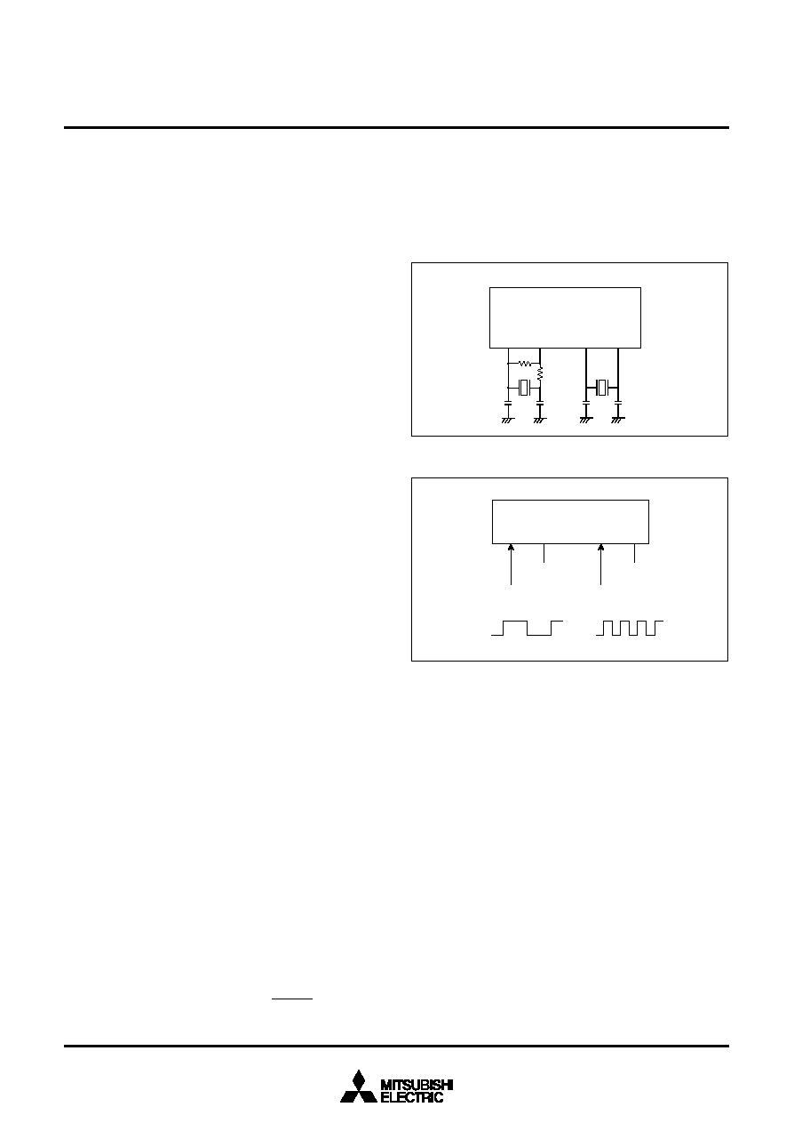
58
3886 Group
SINGLE-CHIP 8-BIT CMOS MICROCOMPUTER
MITSUBISHI MICROCOMPUTERS
CLOCK GENERATING CIRCUIT
The 3886 group has two built-in oscillation circuits. An oscillation
circuit can be formed by connecting a resonator between X
IN
and
X
OUT
(X
CIN
and X
COUT
). Use the circuit constants in accordance
with the resonator manufacturer's recommended values. No exter-
nal resistor is needed between X
IN
and X
OUT
since a feed-back
resistor exists on-chip. However, an external feed-back resistor is
needed between X
CIN
and X
COUT
.
Immediately after power on, only the X
IN
oscillation circuit starts
oscillating, and X
CIN
and X
COUT
pins function as I/O ports.
Frequency Control
(1) Middle-speed mode
The internal clock
is the frequency of X
IN
divided by 8. After re-
set, this mode is selected.
(2) High-speed mode
The internal clock
is half the frequency of X
IN
.
(3) Low-speed mode
The internal clock
is half the frequency of X
CIN
.
s
Note
If you switch the mode between middle/high-speed and low-
speed, stabilize both X
IN
and X
CIN
oscillations. The sufficient time
is required for the sub clock to stabilize, especially immediately af-
ter power on and at returning from stop mode. When switching the
mode between middle/high-speed and low-speed, set the fre-
quency on condition that f(X
IN
) > 3f(X
CIN
).
(4) Low power dissipation mode
The low power consumption operation can be realized by stopping
the main clock X
IN
in low-speed mode. To stop the main clock, set
bit 5 of the CPU mode register to "1." When the main clock X
IN
is
restarted (by setting the main clock stop bit to "0"), set sufficient
time for oscillation to stabilize.
Oscillation Control
(1) Stop mode
If the STP instruction is executed, the internal clock
stops at an
"H" level, and X
IN
and X
CIN
oscillators stop. When the oscillation
stabilizing time set after STP instruction released bit is "0," the
prescaler 12 is set to "FF
16
" and timer 1 is set to "01
16
." When the
oscillation stabilizing time set after STP instruction released bit is
"1," set the sufficient time for oscillation of used oscillator to stabi-
lize since nothing is set to the prescaler 12 and timer 1.
Either X
IN
or X
CIN
divided by 16 is input to the prescaler 12 as
count source, and the output of the prescaler 12 is connected to
timer 1. Set the timer 1 interrupt enable bit to disabled ("0") before
executing the STP instruction. Oscillator restarts when an external
interrupt is received, but the internal clock
is not supplied to the
CPU (remains at "H") until timer 1 underflows. The internal clock
is supplied for the first time, when timer 1 underflows. Therefore
make sure not to set the timer 1 interrupt request bit to "1" before
the STP instruction stops the oscillator. When the oscillator is re-
started by reset, apply "L" level to the RESET pin until the
oscillation is stable since a wait time will not be generated.
(2) Wait mode
If the WIT instruction is executed, the internal clock
stops at an
"H" level, but the oscillator does not stop. The internal clock
re-
starts at reset or when an interrupt is received. Since the oscillator
does not stop, normal operation can be started immediately after
the clock is restarted.
Fig. 58 Ceramic resonator circuit
Fig. 59 External clock input circuit
X
CIN
X
COUT
X
IN
X
OUT
C
IN
C
OUT
C
CIN
C
COUT
Rf
Rd
V
C
C
V
S
S
X
C
I
N
X
C
O
U
T
X
I
N
X
O
U
T
O
p
e
n
O
p
e
n
E
x
t
e
r
n
a
l
o
s
c
i
l
l
a
t
i
o
n
c
i
r
c
u
i
t
E
x
t
e
r
n
a
l
o
s
c
i
l
l
a
t
i
o
n
c
i
r
c
u
i
t
V
C
C
V
S
S
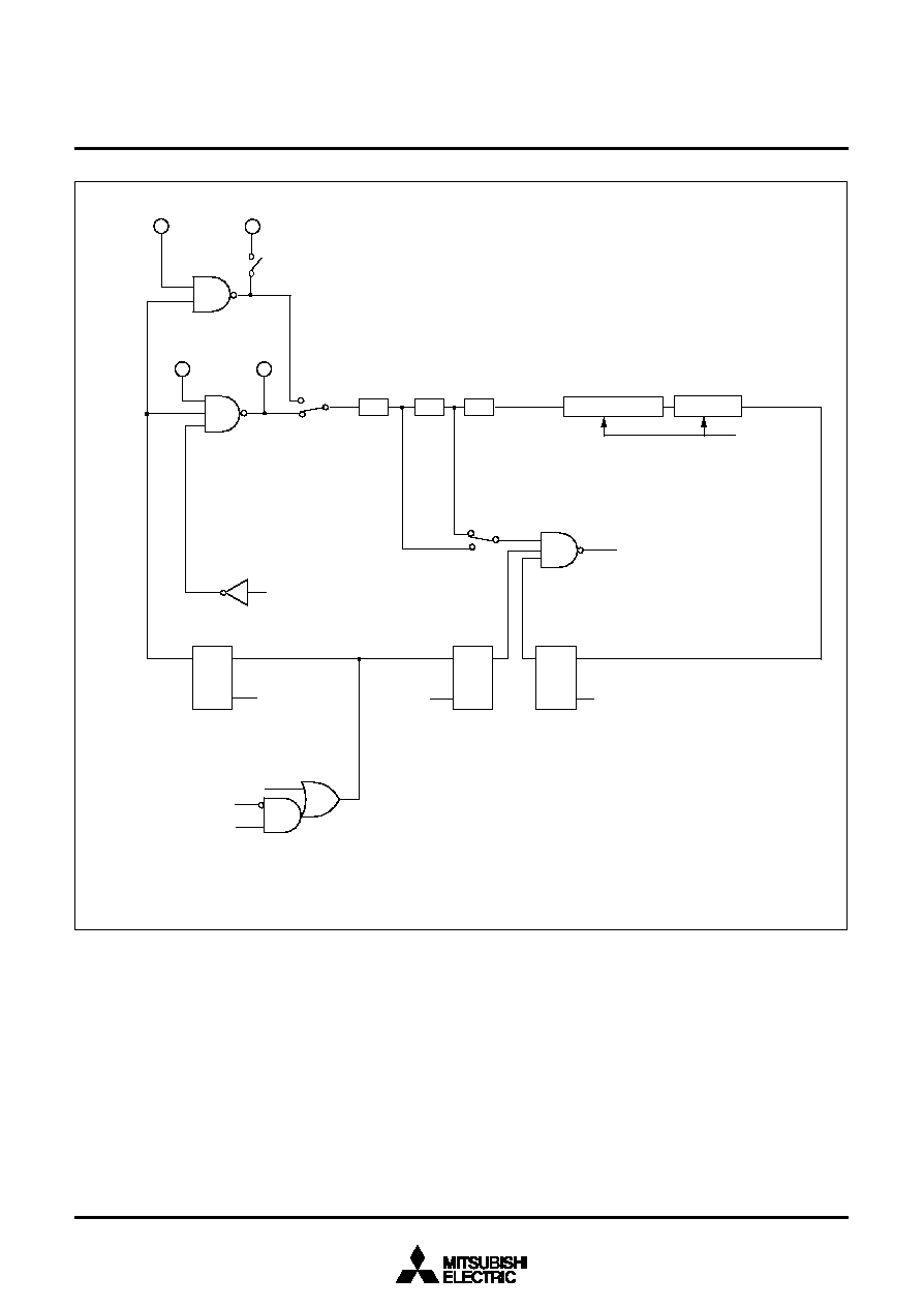
59
3886 Group
SINGLE-CHIP 8-BIT CMOS MICROCOMPUTER
MITSUBISHI MICROCOMPUTERS
Fig. 60 System clock generating circuit block diagram (Single-chip mode)
W
I
T
i
n
s
t
r
u
c
t
i
o
n
S
T
P
i
n
s
t
r
u
c
t
i
o
n
T
i
m
i
n
g
(
i
n
t
e
r
n
a
l
c
l
o
c
k
)
S
R
Q
S
T
P
i
n
s
t
r
u
c
t
i
o
n
S
R
Q
M
a
i
n
c
l
o
c
k
s
t
o
p
b
i
t
S
R
Q
1
/
2
1
/
4
X
I
N
X
O
U
T
X
C
O
U
T
X
C
I
N
I
n
t
e
r
r
u
p
t
r
e
q
u
e
s
t
R
e
s
e
t
I
n
t
e
r
r
u
p
t
d
i
s
a
b
l
e
f
l
a
g
l
1
/
2
P
o
r
t
X
C
s
w
i
t
c
h
b
i
t
"
1
"
"
0
"
L
o
w
-
s
p
e
e
d
m
o
d
e
H
i
g
h
-
s
p
e
e
d
o
r
m
i
d
d
l
e
-
s
p
e
e
d
m
o
d
e
M
i
d
d
l
e
-
s
p
e
e
d
m
o
d
e
H
i
g
h
-
s
p
e
e
d
o
r
l
o
w
-
s
p
e
e
d
m
o
d
e
M
a
i
n
c
l
o
c
k
d
i
v
i
s
i
o
n
r
a
t
i
o
s
e
l
e
c
t
i
o
n
b
i
t
s
(
N
o
t
e
)
N
o
t
e
:
E
i
t
h
e
r
h
i
g
h
-
s
p
e
e
d
,
m
i
d
d
l
e
-
s
p
e
e
d
o
r
l
o
w
-
s
p
e
e
d
m
o
d
e
i
s
s
e
l
e
c
t
e
d
b
y
b
i
t
s
7
a
n
d
6
o
f
t
h
e
C
P
U
m
o
d
e
r
e
g
i
s
t
e
r
.
W
h
e
n
l
o
w
-
s
p
e
e
d
m
o
d
e
i
s
s
e
l
e
c
t
e
d
,
s
e
t
p
o
r
t
X
c
s
w
i
t
c
h
b
i
t
(
b
4
)
t
o
"
1
"
.
M
a
i
n
c
l
o
c
k
d
i
v
i
s
i
o
n
r
a
t
i
o
s
e
l
e
c
t
i
o
n
b
i
t
s
(
N
o
t
e
)
F
F
1
6
0
1
1
6
P
r
e
s
c
a
l
e
r
1
2
T
i
m
e
r
1
R
e
s
e
t
o
r
S
T
P
i
n
s
t
r
u
c
t
i
o
n
60
3886 Group
SINGLE-CHIP 8-BIT CMOS MICROCOMPUTER
MITSUBISHI MICROCOMPUTERS
Fig. 61 State transitions of system clock
C
M
4
:
P
o
r
t
X
c
s
w
i
t
c
h
b
i
t
0
:
I
/
O
p
o
r
t
f
u
n
c
t
i
o
n
(
s
t
o
p
o
s
c
i
l
l
a
t
i
n
g
)
1
:
X
C
I
N
-
X
C
O
U
T
o
s
c
i
l
l
a
t
i
n
g
f
u
n
c
t
i
o
n
C
M
5
:
M
a
i
n
c
l
o
c
k
(
X
I
N
-
X
O
U
T
)
s
t
o
p
b
i
t
0
:
O
p
e
r
a
t
i
n
g
1
:
S
t
o
p
p
e
d
C
M
7
,
C
M
6
:
M
a
i
n
c
l
o
c
k
d
i
v
i
s
i
o
n
r
a
t
i
o
s
e
l
e
c
t
i
o
n
b
i
t
b
7
b
6
0
0
:
=
f
(
X
I
N
)
/
2
(
H
i
g
h
-
s
p
e
e
d
m
o
d
e
)
0
1
:
=
f
(
X
I
N
)
/
8
(
M
i
d
d
l
e
-
s
p
e
e
d
m
o
d
e
)
1
0
:
=
f
(
X
C
I
N
)
/
2
(
L
o
w
-
s
p
e
e
d
m
o
d
e
)
1
1
:
N
o
t
a
v
a
i
l
a
b
l
e
N
o
t
e
s
R
e
s
e
t
C
M
4
"
1
"
"
0
"
C
M
4
"
0
"
"
1
"
C
M
6
"
1
"
"
0
"
C
M
4
"
1
"
"
0
"
C
M
6
"
1
"
"
0
"
C
M
7
"
1
"
"
0
"
C
M
4
"
1
"
"
0
"
C
M
5
"
1
"
"
0
"
C
M
6
"
1
"
"
0
"
C
M
6
"
1
"
"
0
"
C
P
U
m
o
d
e
r
e
g
i
s
t
e
r
b
7
b
4
C
M
7
"
0
"
"
1
"
C
M
6
"
1
"
"
0
"
(
C
P
U
M
:
a
d
d
r
e
s
s
0
0
3
B
1
6
)
C
M
7
=
0
C
M
6
=
1
C
M
5
=
0
(
1
0
M
H
z
o
s
c
i
l
l
a
t
i
n
g
)
C
M
4
=
0
(
3
2
k
H
z
s
t
o
p
p
e
d
)
M
i
d
d
l
e
-
s
p
e
e
d
m
o
d
e
(
f
(
)
=
1
.
2
5
M
H
z
)
C
M
7
=
0
C
M
6
=
1
C
M
5
=
0
(
1
0
M
H
z
o
s
c
i
l
l
a
t
i
n
g
)
C
M
4
=
1
(
3
2
k
H
z
o
s
c
i
l
l
a
t
i
n
g
)
M
i
d
d
l
e
-
s
p
e
e
d
m
o
d
e
(
f
(
)
=
1
.
2
5
M
H
z
)
C
M
7
=
0
C
M
6
=
0
C
M
5
=
0
(
1
0
M
H
z
o
s
c
i
l
l
a
t
i
n
g
)
C
M
4
=
0
(
3
2
k
H
z
s
t
o
p
p
e
d
)
H
i
g
h
-
s
p
e
e
d
m
o
d
e
(
f
(
)
=
5
M
H
z
)
C
M
7
=
1
C
M
6
=
0
C
M
5
=
0
(
1
0
M
H
z
o
s
c
i
l
l
a
t
i
n
g
)
C
M
4
=
1
(
3
2
k
H
z
o
s
c
i
l
l
a
t
i
n
g
)
L
o
w
-
s
p
e
e
d
m
o
d
e
(
f
(
)
=
1
6
k
H
z
)
C
M
7
=
1
C
M
6
=
0
C
M
5
=
1
(
1
0
M
H
z
s
t
o
p
p
e
d
)
C
M
4
=
1
(
3
2
k
H
z
o
s
c
i
l
l
a
t
i
n
g
)
L
o
w
-
s
p
e
e
d
m
o
d
e
(
f
(
)
=
1
6
k
H
z
)
C
M
7
=
0
C
M
6
=
0
C
M
5
=
0
(
1
0
M
H
z
o
s
c
i
l
l
a
t
i
n
g
)
C
M
4
=
1
(
3
2
k
H
z
o
s
c
i
l
l
a
t
i
n
g
)
H
i
g
h
-
s
p
e
e
d
m
o
d
e
(
f
(
)
=
5
M
H
z
)
1
:
S
w
i
t
c
h
t
h
e
m
o
d
e
b
y
t
h
e
a
l
l
o
w
s
s
h
o
w
n
b
e
t
w
e
e
n
t
h
e
m
o
d
e
b
l
o
c
k
s
.
(
D
o
n
o
t
s
w
i
t
c
h
b
e
t
w
e
e
n
t
h
e
m
o
d
e
s
d
i
r
e
c
t
l
y
w
i
t
h
o
u
t
a
n
a
l
l
o
w
.
)
2
:
T
h
e
a
l
l
m
o
d
e
s
c
a
n
b
e
s
w
i
t
c
h
e
d
t
o
t
h
e
s
t
o
p
m
o
d
e
o
r
t
h
e
w
a
i
t
m
o
d
e
a
n
d
r
e
t
u
r
n
t
o
t
h
e
s
o
u
r
c
e
m
o
d
e
w
h
e
n
t
h
e
s
t
o
p
m
o
d
e
o
r
t
h
e
w
a
i
t
m
o
d
e
i
s
e
n
d
e
d
.
3
:
T
i
m
e
r
o
p
e
r
a
t
e
s
i
n
t
h
e
w
a
i
t
m
o
d
e
.
4
:
W
h
e
n
t
h
e
s
t
o
p
m
o
d
e
i
s
e
n
d
e
d
,
a
d
e
l
a
y
o
f
a
p
p
r
o
x
i
m
a
t
e
l
y
1
m
s
o
c
c
u
r
s
b
y
c
o
n
n
e
c
t
i
n
g
p
r
e
s
c
a
l
e
r
1
2
a
n
d
T
i
m
e
r
1
i
n
m
i
d
d
l
e
/
h
i
g
h
-
s
p
e
e
d
m
o
d
e
.
5
:
W
h
e
n
t
h
e
s
t
o
p
m
o
d
e
i
s
e
n
d
e
d
,
a
d
e
l
a
y
o
f
a
p
p
r
o
x
i
m
a
t
e
l
y
0
.
2
5
s
o
c
c
u
r
s
b
y
T
i
m
e
r
1
a
n
d
T
i
m
e
r
2
i
n
l
o
w
-
s
p
e
e
d
m
o
d
e
.
6
: W
a
i
t
u
n
t
i
l
o
s
c
i
l
l
a
t
i
o
n
s
t
a
b
i
l
i
z
e
s
a
f
t
e
r
o
s
c
i
l
l
a
t
i
n
g
t
h
e
m
a
i
n
c
l
o
c
k
X
I
N
b
e
f
o
r
e
t
h
e
s
w
i
t
c
h
i
n
g
f
r
o
m
t
h
e
l
o
w
-
s
p
e
e
d
m
o
d
e
t
o
m
i
d
d
l
e
/
h
i
g
h
-
s
p
e
e
d
m
o
d
e
.
7
:
T
h
e
e
x
a
m
p
l
e
a
s
s
u
m
e
s
t
h
a
t
1
0
M
H
z
i
s
b
e
i
n
g
a
p
p
l
i
e
d
t
o
t
h
e
X
I
N
p
i
n
a
n
d
3
2
k
H
z
t
o
t
h
e
X
C
I
N
p
i
n
.
i
n
d
i
c
a
t
e
s
t
h
e
i
n
t
e
r
n
a
l
c
l
o
c
k
.
61
3886 Group
SINGLE-CHIP 8-BIT CMOS MICROCOMPUTER
MITSUBISHI MICROCOMPUTERS
PROCESSOR MODE
Single-chip mode, memory expansion mode, and microprocessor
mode in the M38867M8A/E8A can be selected by changing the
contents of the processor mode bits (CM
0
and CM
1
: b1 and b0 of
address 003B
16
). In memory expansion mode and microprocessor
mode, memory can be expanded externally through ports P0 to
P3. In these modes, ports P0 to P3 lose their I/O port functions
and become bus pins.
Fig. 62 Memory maps in various processor modes
Fig. 63 Structure of CPU mode register
(1) Single-chip mode
Select this mode by resetting the microcomputer with CNV
SS
con-
nected to V
SS
.
(2) Memory expansion mode
Select this mode by setting the processor mode bits (b1, b0) to
"01" in software with CNV
SS
connected to V
SS
. This mode enables
external memory expansion while maintaining the validity of the in-
ternal ROM.
However, do not set this mode in the M38869M8A/MCA/MFA and
the flash memory version.
(3) Microprocessor mode
Select this mode by resetting the microcomputer with CNV
SS
con-
nected to V
CC
, or by setting the processor mode bits to "10" in
software with CNV
SS
connected to V
SS
. In microprocessor mode,
the internal ROM is no longer valid and external memory must be
used.
Do not set this mode in the M38869M8A/MCA/MFA and the flash
memory version.
Port Name
Port P0
Port P1
Port P2
Port P3
Function
Outputs low-order 8 bits of address.
Outputs high-order 8 bits of address.
Operates as I/O pins for data D
7
to D
0
(including instruction code).
P3
0
and P3
1
function only as output pins
(except that the port latch cannot be read).
P3
2
is the ONW input pin.
P3
3
is the RESET
OUT
output pin. (Note)
P3
4
is the
output pin.
P3
5
is the SYNC output pin.
P3
6
is the WR output pin, and P3
7
is the RD out-
put pin.
Table 15 Port functions in memory expansion mode and
microprocessor mode
Note : If CNV
SS
is connected to V
SS
, the microcomputer goes to single-
chip mode after a reset, so that this pin cannot be used as the
RESET
OUT
output pin.
X
X
X
X
1
6
0
0
0
0
1
6
0
0
4
0
1
6
0
0
0
8
1
6
0
0
0
0
1
6
Y
Y
Y
Y
1
6
F
F
F
F
1
6
0
0
0
8
1
6
0
0
4
0
1
6
F
F
F
F
1
6
I
n
t
e
r
n
a
l
R
A
M
r
e
s
e
r
v
e
d
a
r
e
a
I
n
t
e
r
n
a
l
R
O
M
M
e
m
o
r
y
e
x
p
a
n
s
i
o
n
m
o
d
e
T
h
e
s
h
a
d
e
d
a
r
e
a
a
r
e
e
x
t
e
r
n
a
l
m
e
m
o
r
y
a
r
e
a
.
S
F
R
a
r
e
a
X
X
X
X
1
6
i
n
d
i
c
a
t
e
s
t
h
e
l
a
s
t
a
d
d
r
e
s
s
o
f
i
n
t
e
r
n
a
l
R
A
M
.
Y
Y
Y
Y
1
6
i
n
d
i
c
a
t
e
s
t
h
e
f
i
r
s
t
a
d
d
r
e
s
s
o
f
i
n
t
e
r
n
a
l
R
O
M
.
S
F
R
a
r
e
a
M
i
c
r
o
p
r
o
c
e
s
s
o
r
m
o
d
e
*
*
:
I
n
t
e
r
n
a
l
R
A
M
r
e
s
e
r
v
e
d
a
r
e
a
X
X
X
X
1
6
*
*
b
0
C
P
U
m
o
d
e
r
e
g
i
s
t
e
r
(
C
P
U
M
:
a
d
d
r
e
s
s
0
0
3
B
1
6
)
P
r
o
c
e
s
s
o
r
m
o
d
e
b
i
t
s
(
C
M
1
,
C
M
0
)
b
1
b
0
0
0
:
S
i
n
g
l
e
-
c
h
i
p
m
o
d
e
0
1
:
M
e
m
o
r
y
e
x
p
a
n
s
i
o
n
m
o
d
e
(N
o
t
e)
1
0
:
M
i
c
r
o
p
r
o
c
e
s
s
o
r
m
o
d
e
(N
o
t
e)
1
1
:
N
o
t
a
v
a
i
l
a
b
l
e
S
t
a
c
k
p
a
g
e
s
e
l
e
c
t
i
o
n
b
i
t
0
:
0
p
a
g
e
1
:
1
p
a
g
e
b
7
N
o
t
e
:
T
h
i
s
i
s
n
o
t
a
v
a
i
l
a
b
l
e
f
o
r
t
h
e
p
r
o
d
u
c
t
s
e
x
c
e
p
t
M
3
8
8
6
7
M
8
A
/
E
8
A
.
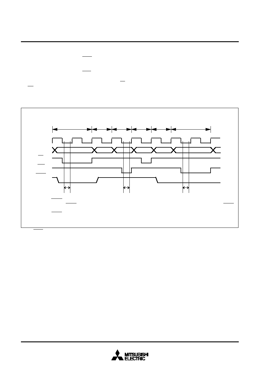
62
3886 Group
SINGLE-CHIP 8-BIT CMOS MICROCOMPUTER
MITSUBISHI MICROCOMPUTERS
BUS CONTROL AT MEMORY EXPANSION
The M38867M8A/E8A have a built-in ONW function to facilitate
access to an external (expanded) memory and I/O devices in
memory expansion mode or microprocessor mode.
If an "L" level signal is input to the P3
2
/ONW pin when the CPU is
in a read or write state, the corresponding read or write cycle is
extended by one cycle of
. During this extended term, the RD
and WR signals remain at "L." This extension function is valid only
for writing to and reading from addresses 0000
16
to 0007
16
and
0440
16
to FFFF
16
, and only read and write cycles are extended.
Fig. 64 ONW function timing
R
D
W
R
O
N
W
*
*
*
*
T
e
r
m
w
h
e
r
e
O
N
W
i
n
p
u
t
s
i
g
n
a
l
i
s
r
e
c
e
i
v
e
d
.
D
u
r
i
n
g
t
h
i
s
t
e
r
m
,
t
h
e
O
N
W
s
i
g
n
a
l
m
u
s
t
b
e
f
i
x
e
d
a
t
e
i
t
h
e
r
"
H
"
o
r
"
L
"
.
A
t
a
l
l
o
t
h
e
r
t
i
m
e
s
,
t
h
e
i
n
p
u
t
l
e
v
e
l
o
f
t
h
e
O
N
W
s
i
g
n
a
l
h
a
s
n
o
a
f
f
e
c
t
o
n
o
p
e
r
a
t
i
o
n
s
.
T
h
e
b
u
s
c
y
c
l
e
s
i
s
n
o
t
e
x
t
e
n
d
e
d
f
o
r
a
n
a
d
d
r
e
s
s
i
n
t
h
e
a
r
e
a
0
0
0
8
1
6
t
o
0
4
3
F
1
6
,
b
e
c
a
u
s
e
t
h
e
O
N
W
s
i
g
n
a
l
i
s
n
o
t
r
e
c
e
i
v
e
d
.
R
e
a
d
c
y
c
l
e
W
r
i
t
e
c
y
c
l
e
D
u
m
m
y
c
y
c
l
e W
r
i
t
e
c
y
c
l
e
R
e
a
d
c
y
c
l
e D
u
m
m
y
c
y
c
l
e
A
D
1
5
--
A
D
0
63
3886 Group
SINGLE-CHIP 8-BIT CMOS MICROCOMPUTER
MITSUBISHI MICROCOMPUTERS
EPROM MODE
The built-in PROM of the blank One Time PROM version and built-
in EPROM version can be read or programmed with a
general-purpose PROM programmer using a special programming
adapter. The One Time PROM version and the built-in EPROM
version have the function of the M5M27C101 corresponding for
writing to the built-in PROM. Set the address of PROM program-
mer in the user ROM area.
The PROM of the blank One Time PROM version is not tested or
screened in the assembly process and following processes. To en-
sure proper operation after programming, the procedure shown in
Figure 65 is recommended to verify programming.
Fig. 65 Programming and testing of One Time PROM version
Table 16 Programming adapter
Package
80P6Q-A
80D0
Name of Programming Adapter
PCA4738H-80A
PCA4738L-80A
Table 17 PROM programmer setup
Product name
PROM programmer setup
Corresponding
device
Writing
area
M38867E8AHP
M38867E8AFS
ROM area of
microcomputer
M5M27C101K
byte
program
08080
16
|
0FFFD
16
8080
16
|
FFFD
16
P
r
o
g
r
a
m
m
i
n
g
w
i
t
h
P
R
O
M
p
r
o
g
r
a
m
m
e
r
S
c
r
e
e
n
i
n
g
(
C
a
u
t
i
o
n
)
(
1
5
0
∞
C
f
o
r
4
0
h
o
u
r
s
)
V
e
r
i
f
i
c
a
t
i
o
n
w
i
t
h
P
R
O
M
p
r
o
g
r
a
m
m
e
r
F
u
n
c
t
i
o
n
a
l
c
h
e
c
k
i
n
t
a
r
g
e
t
d
e
v
i
c
e
T
h
e
s
c
r
e
e
n
i
n
g
t
e
m
p
e
r
a
t
u
r
e
i
s
f
a
r
h
i
g
h
e
r
t
h
a
n
t
h
e
s
t
o
r
a
g
e
t
e
m
p
e
r
a
t
u
r
e
.
N
e
v
e
r
e
x
p
o
s
e
t
o
1
5
0
∞
C
e
x
c
e
e
d
i
n
g
1
0
0
h
o
u
r
s
.
C
a
u
t
i
o
n
:
64
3886 Group
SINGLE-CHIP 8-BIT CMOS MICROCOMPUTER
MITSUBISHI MICROCOMPUTERS
FLASH MEMORY MODE
The M38869FFAHP/GP has the flash memory mode in addition to
the normal operation mode (microcomputer mode). The user can
use this mode to perform read, program, and erase operations for
the internal flash memory.
The M38869FFAHP/GP has three modes the user can choose:
the parallel input/output and serial input/output mode, where the
flash memory is handled by using the external programmer, and
the CPU reprogramming mode, where the flash memory is
handled by the central processing unit (CPU). The following ex-
plains these modes.
(1) Flash memory mode 1 (parallel I/O mode)
The parallel I/O mode can be selected by connecting wires as
shown in Figures 65 and supplying power to the V
CC
and V
PP
pins. In this mode, the M38869FFAHP/GP operates as an equiva-
lent of MITSUBISHI's CMOS flash memory M5M28F101.
However, because the M38869FFAHP/GP's internal memory has
a capacity of 60 Kbytes, programming is available for addresses
01000
16
to 0FFFF
16
, and make sure that the data in addresses
00000
16
to 00FFF
16
and addresses 10000
16
to 1FFFF
16
are FF
16
.
Note also that the M38869FFAHP/GP does not contain a facility to
read out a device identification code by applying a high voltage to
address input (A9). Be careful not to erratically set program condi-
tions when using a general-purpose PROM programmer.
Table 18 shows the pin assignments when operating in the paral-
lel input/output mode.
Table 18 Pin assignments of M38869FFAHP/GP when
operating in the parallel input/output mode
V
CC
V
PP
V
SS
Address input
Data I/O
__
CE
___
OE
___
WE
M38869FFAHP/GP
V
CC
CNV
SS
V
SS
Ports P0, P1, P3
1
Port P2
P3
6
P3
7
P3
3
M5M28F101
V
CC
V
PP
V
SS
A
0
≠A
16
D
0
≠D
7
__
CE
__
OE
___
WE
Functional Outline (parallel input/output mode)
In the parallel input/output mode, the M38869FFAHP/GP allow the
user to choose an operation mode between the read-only mode
and the read/write mode (software command control mode) de-
pending on the voltage applied to the V
PP
pin. When V
PP
= V
PP
L,
the read-only mode is selected, and the user can choose one of
three states (e.g., read, output disable, or standby) depending on
___ ___
___
inputs to the CE, OE, and WE pins. When V
PP
= V
PP
H, the read/
write mode is selected, and the user can choose one of four states
(e.g., read, output disable, standby, or write) depending on inputs
__
__
___
to the CE, OE, and WE pins. Table 19 shows assignment states of
control input and each state.
q
Read
__
The microcomputer enters the read state by driving the CE, and
__
___
OE pins low and the WE pin high; and the contents of memory
corresponding to the address to be input to address input pins
(A
0
≠A
16
).
are output to the data input/output pins (D
0
≠D
7
).
q
Output disable
The microcomputer enters the output disable state by driving the
__
___
__
CE pin low and the WE and OE pins high; and the data input/out-
put pins enter the floating state.
q
Standby
__
The microcomputer enters the standby state by driving the CE pin
high. the M38869FFAHP/GP is placed in a power-down state con-
suming only a minimal supply current. At this time, the data input/
output pins enter the floating state.
q
Write
The microcomputer enters the write state by driving the V
PP
pin
___
__
high (V
PP
= V
PP
H) and then the WE pin low when the CE pin is
__
low and the OE pin is high. In this state, software commands can
be input from the data input/output pins, and the user can choose
program or erase operation depending on the contents of this soft-
ware command.
Pin
Mode
Read
Output disable
Standby
Read
Output disable
Standby
Write
Read-only
Read/Write
__
CE
V
IL
V
IL
V
IH
V
IL
V
IL
V
IH
V
IL
V
IL
V
IH
◊
V
IL
V
IH
◊
V
IH
Table 19 Assignment sates of control input and each state
__
OE
___
WE
V
IH
V
IH
◊
V
IH
V
IH
◊
V
IL
V
PP
L
V
PP
L
V
PP
L
V
PP
H
V
PP
H
V
PP
H
V
PP
H
V
PP
Output
Floating
Floating
Output
Floating
Floating
Input
Data I/O
Note:
◊
can be V
IL
or V
IH
.
State
65
3886 Group
SINGLE-CHIP 8-BIT CMOS MICROCOMPUTER
MITSUBISHI MICROCOMPUTERS
Supply 5 V ± 10 % to V
CC
and 0 V to V
SS
.
Connect to 5 V ± 10 % in read-only mode, connect to 11.7 to 12.6 V in read/write mode.
Connect to V
SS
.
Connect a ceramic resonator between X
IN
and X
OUT
.
Connect to V
SS
.
Connect to V
SS
.
Port P0 functions as 8-bit address input (A
0
≠A
7
).
Port P1 functions as 8-bit address input (A
8
≠A
15
).
Function as 8-bit data's I/O pins (D
0
≠D
7
).
__
__
___
P3
7
, P3
6
and P3
3
function as the OE, CE and WE input pins respectively. P3
1
functions as
the A
16
input pin. Connect P3
0
and P3
2
to V
SS
. Input "H" or "L" to P3
4
, P3
5
, or keep
them open.
Connect P4
4
, P4
6
to V
SS
. Input "H" or "L" to P4
0
- P4
3,
P4
5
, P4
7
, or keep them open.
Input "H" or "L", or keep them open.
Input "H" or "L", or keep them open.
Input "H" or "L", or keep them open.
Input "H" or "L", or keep them open.
Power supply
V
PP
input
Reset input
Clock input
Clock output
Analog supply input
Reference voltage input
Address input (A
0
≠A
7
)
Address input (A
8
≠A
15
)
Data I/O (D
0
≠D
7
)
Control signal input
Input port P4
Input port P5
Input port P6
Input port P7
Input port P8
Table 20 Pin description (flash memory parallel I/O mode)
Pin
Name
--
Input
Input
Input
Output
--
Input
Input
Input
I/O
Input
Input
Input
Input
Input
Input
Input
/Output
Functions
V
CC
, V
SS
CNV
SS
_____
RESET
X
IN
X
OUT
AV
SS
V
REF
P0
0
≠P0
7
P1
0
≠P1
7
P2
0
≠P2
7
P3
0
≠P3
7
P4
0
≠P4
7
P5
0
≠P5
7
P6
0
≠P6
7
P7
0
≠P7
7
P8
0
≠P8
7
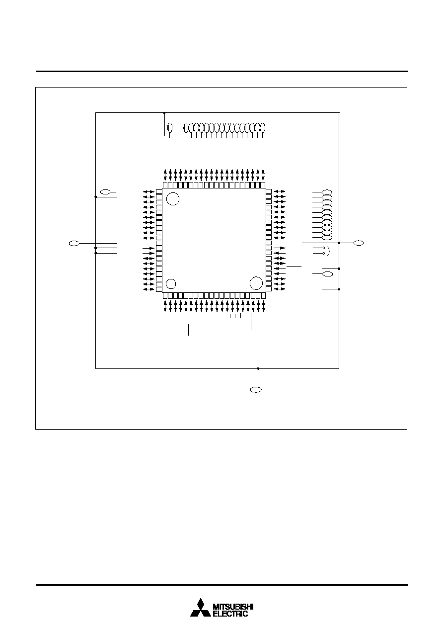
66
3886 Group
SINGLE-CHIP 8-BIT CMOS MICROCOMPUTER
MITSUBISHI MICROCOMPUTERS
Fig. 66 Pin connection of M38869FFAHP/GP when operating in parallel input/output mode
1
2
3
4
7
8
9 1
0 1
1 1
2 1
3 1
4 1
5 1
6 1
7 1
8 1
9 2
0
5
6
2
1
2
2
2
3
2
4
2
5
2
6
2
7
2
8
2
9
3
0
3
1
3
2
3
3
3
4
3
5
3
6
3
7
3
8
3
9
4
0
4
1
4
2
4
3
4
4
4
5
4
6
4
7
4
8
4
9
5
0
5
1
5
2
5
3
5
4
5
5
5
6
5
7
5
8
5
9
6
0
6
1
6
2
6
3
6
4
6
5
6
6
6
7
6
8
6
9
7
0
7
1
7
2
7
3
7
4
7
5
7
6
7
7
7
8
7
9
8
0
P
3
0
/
P
W
M
0
0
P
3
1
/
P
W
M
1
0
P
6
2
/
A
N
2
P
6
1
/
A
N
1
P
6
0
/
A
N
0
P
7
7
/
S
C
L
P
7
6
/
S
D
A
P
7
5
/
I
N
T
4
1
P
7
4
/
I
N
T
3
1
P
7
2
/
S
C
L
K
2
P
7
1
/
S
O
U
T
2
P
7
0
/
S
I
N
2
P
5
7
/
D
A
2
/
P
W
M
1
1
P
5
0
/
A
0
P
4
5
/
T
X
D
P
4
4
/
R
X
D
P
4
3
/
I
N
T
1
/
O
B
F
0
1
P
6
3
/
A
N
3
P
6
4
/
A
N
4
P
6
5
/
A
N
5
P
6
6
/
A
N
6
A
V
S
S
P
6
7
/
A
N
7
V
R
E
F
V
C
C
P
8
0
/
D
Q
0
P
8
1
/
D
Q
1
P
8
2
/
D
Q
2
P
8
3
/
D
Q
3
P
8
4
/
D
Q
4
P
8
5
/
D
Q
5
P
8
6
/
D
Q
6
P
8
7
/
D
Q
7
P
4
2
/
I
N
T
0
/
O
B
F
0
0
C
N
V
S
S
X
I
N
X
O
U
T
V
S
S
R
E
S
E
T
P
7
3
/
S
R
D
Y
2
/
I
N
T
2
1
P
5
5
/
C
N
T
R
1
P
5
4
/
C
N
T
R
0
P
5
6
/
D
A
1
/
P
W
M
0
1
P
4
0
/
X
C
O
U
T
P
4
1
/
X
C
I
N
P
4
7
/
S
R
D
Y
1
/
S
1
P
5
2
/
I
N
T
3
0
/
R
P
5
3
/
I
N
T
4
0
/
W
P
5
1
/
I
N
T
2
0
/
S
0
P
3
4
P
3
5
P
0
0
/
P
3
R
E
F
P
0
4
P
0
5
P
0
6
P
0
7
P
1
1
P
1
2
P
1
3
P
1
4
P
1
5
P
1
6
P
1
7
P
2
6
P
2
5
P
2
4
P
2
3
P
2
2
P
2
1
P
2
0
P
1
0
P
0
1
P
0
2
P
3
2
P
3
3
P
3
6
P
3
7
P
0
3
P
2
7
P
4
6
/
S
C
L
K
1
/
O
B
F
1
0
M
3
8
8
6
9
F
F
A
H
P
M
3
8
8
6
9
F
F
AGP
V
p
p
D
7
A
1
4
D
0
D
1
D
2
D
3
D
4
D
5
D
6
A
1
5
A
0
A
1
A
2
A
3
A
4
A
5
A
6
A
7
A
8
A
9
A
1
0
A
1
1
A
1
2
A
1
3
V
s
s
V
c
c
O
E
C
E
W
E
A
1
6
*
:
C
o
n
n
e
c
t
t
o
t
h
e
c
e
r
a
m
i
c
o
s
c
i
l
l
a
t
i
o
n
c
i
r
c
u
i
t
.
i
n
d
i
c
a
t
e
s
t
h
e
f
l
a
s
h
m
e
m
o
r
y
p
i
n
.
*
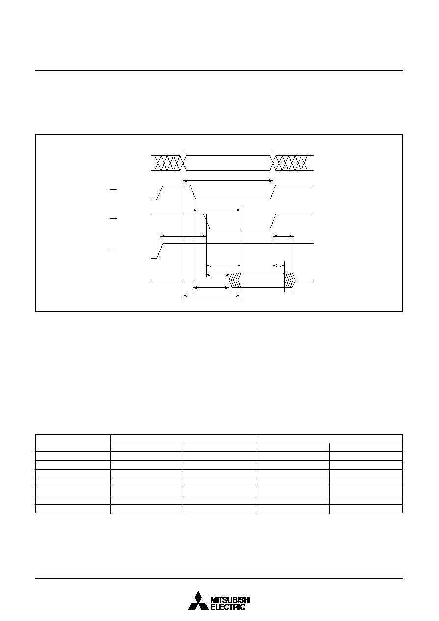
67
3886 Group
SINGLE-CHIP 8-BIT CMOS MICROCOMPUTER
MITSUBISHI MICROCOMPUTERS
Read-only Mode
The microcomputer enters the read-only mode by applying V
PP
L
to the V
PP
pin. In this mode, the user can input the address of a
memory location to be read and the control signals at the timing
shown in Figure 67, and the M38869FFAHP/GP will output the
contents of the user's specified address from data I/O pin to the
external. In this mode, the user cannot perform any operation
other than read.
Fig. 67 Read timing
Read/Write Mode
The microcomputer enters the read/write mode by applying V
PP
H
to the V
PP
pin. In this mode, the user must first input a software
command to choose the operation (e. g., read, program, or erase)
to be performed on the flash memory (this is called the first cycle),
and then input the information necessary for execution of the com-
mand (e.g, address and data) and control signals (this is called
the second cycle). When this is done, the M38869FFAHP/GP ex-
ecutes the specified operation.
Table 21 shows the software commands and the input/output in-
formation in the first and the second cycles. The input address is
___
latched internally at the falling edge of the WE input; software
commands and other input data are latched internally at the rising
___
edge of the WE input.
The following explains each software command. Refer to Figures 68
to 70 for details about the signal input/output timings.
Table 21 Software command (Parallel input/output mode)
Symbol
Read
Program
Program verify
Erase
Erase verify
Reset
Device identification
Address input
◊
◊
◊
◊
Verify address
◊
◊
First cycle
Data input
00
16
40
16
C0
16
20
16
A0
16
FF
16
90
16
Address input
Read address
Program address
◊
◊
◊
◊
ADI
Second cycle
Data I/O
Read data (Output)
Program data (Input)
Verify data (Output)
20
16
(Input)
Verify data (Output)
FF
16
(Input)
DDI (Output)
Note: ADI = Device identification address : manufacturer's code 00000
16
, device code 00001
16
DDI = Device identification data : manufacturer's code 1C
16
, device code D0
16
X can be V
IL
or V
IH
.
Address
Valid address
t
RC
t
a(CE)
t
WRR
t
DF
t
a(OE)
t
DH
t
OLZ
Floating
Floating
t
CLZ
t
a(AD)
V
IH
V
IL
V
IH
V
IL
V
IH
V
IL
V
IH
V
IL
V
OH
V
OL
CE
OE
WE
Data
Dout
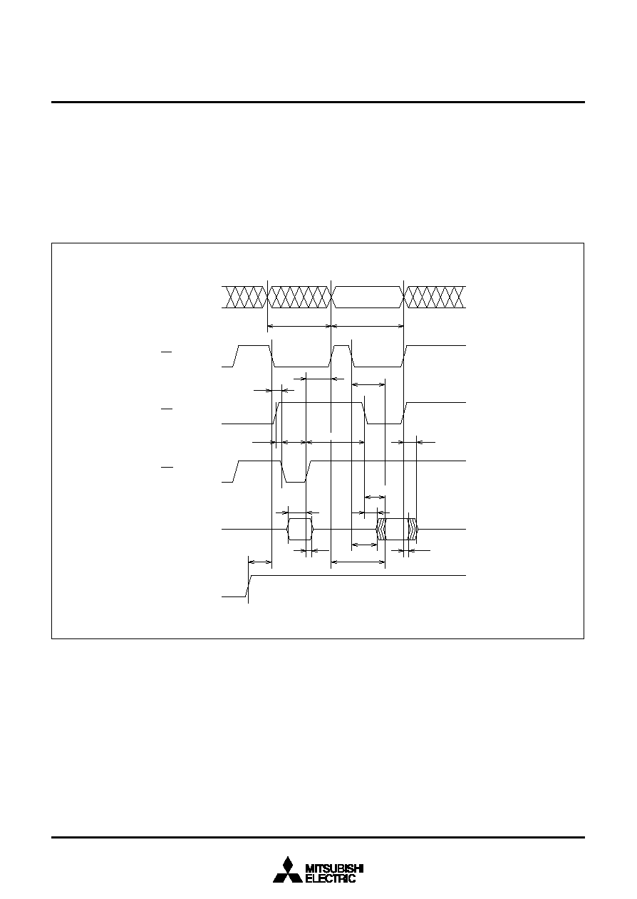
68
3886 Group
SINGLE-CHIP 8-BIT CMOS MICROCOMPUTER
MITSUBISHI MICROCOMPUTERS
q
Read command
The microcomputer enters the read mode by inputting command
code "00
16
" in the first cycle. The command code is latched into
___
the internal command latch at the rising edge of the WE input.
When the address of a memory location to be read is input in the
second cycle, with control signals input at the timing shown in
Figure 68, the M38869FFAHP/GP outputs the contents of the
specified address from the data I/O pins to the external.
The read mode is retained until any other command is latched into
the command latch. Consequently, once the M38869FFAHP/GP en-
ters the read mode, the user can read out the successive memory
contents simply by changing the input address and executing the
second cycle only. Any command other than the read command
must be input beginning from its command code over again each
time the user execute it. The contents of the command latch immedi-
ately after power-on is 00
16
.
Fig. 68 Timings during reading
Address
Valid address
t
WC
t
CH
t
CS
t
RC
t
a(CE)
t
DF
t
WRR
t
WP
t
RRW
t
a(OE)
t
DH
t
DH
t
VSC
t
CLZ
t
OLZ
t
DS
t
a(AD)
V
IH
V
IL
V
IH
V
IL
V
IH
V
IL
V
IH
V
IL
V
IH
V
IL
V
PP
H
V
PP
L
CE
OE
WE
Data
V
PP
Dout
00
16
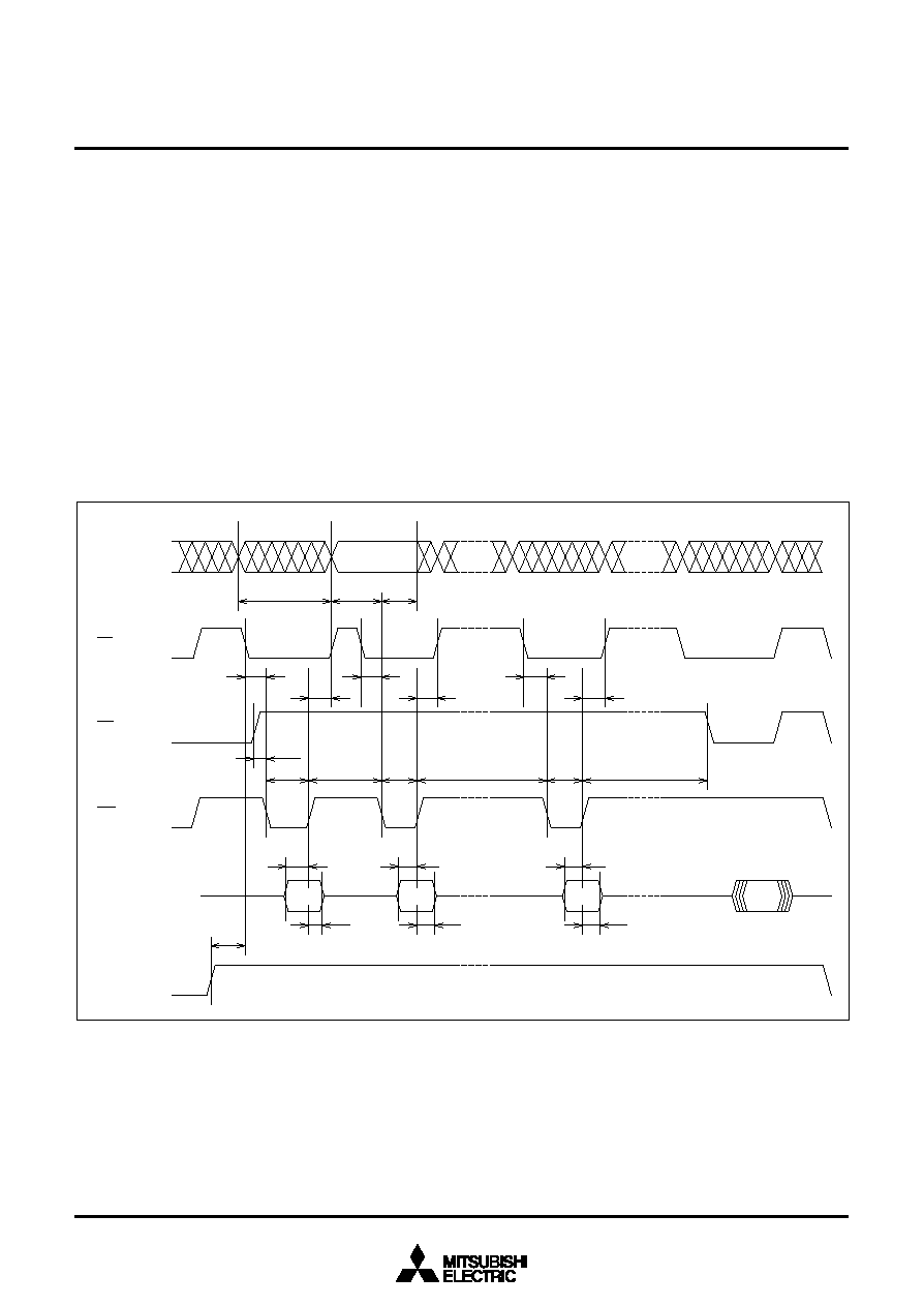
69
3886 Group
SINGLE-CHIP 8-BIT CMOS MICROCOMPUTER
MITSUBISHI MICROCOMPUTERS
q
Program command
The microcomputer enters the program mode by inputting com-
mand code "40
16
" in the first cycle. The command code is latched
___
into the internal command latch at the rising edge of the WE input.
When the address which indicates a program location and data is
input in the second cycle, the M38869FFAHP/GP internally
___
latches the address at the falling edge of the WE input and the
___
data at the rising edge of the WE input. The M38869FFAHP/GP
___
starts programming at the rising edge of the WE input in the sec-
ond cycle and finishes programming within 10
µ
s as measured by
its internal timer. Programming is performed in units of bytes.
Note: A programming operation is not completed by executing the
program command once. Always be sure to execute a pro-
gram verify command after executing the program command.
When the failure is found in this verification, the user must re-
peatedly execute the program command until the pass. Refer
to Figure 71 for the programming flowchart.
q
Program verify command
The microcomputer enters the program verify mode by inputting
command code "C0
16
" in the first cycle. This command is used to
verify the programmed data after executing the program com-
mand. The command code is latched into the internal command
___
latch at the rising edge of the WE input. When control signals are
input in the second cycle at the timing shown in Figure 69, the
M38869FFAHP/GP outputs the programmed address's contents to
the external. Since the address is internally latched when the pro-
gram command is executed, there is no need to input it in the
second cycle.
Fig. 69 Input/output timings during programming (Verify data is output at the same timing as for read.)
Address
Program
Program verify
Program
address
t
WC
t
CS
t
RRW
t
WP
t
WPH
t
WP
t
DP
t
DS
40
16
D
IN
C0
16
Dout
t
DS
t
DH
t
DH
Verify data output
t
DH
t
VSC
t
DS
t
WP
t
WRR
t
CS
t
CS
t
CH
t
CH
t
CH
t
AS
t
AH
V
IH
V
IL
V
IH
V
IL
V
IH
V
IL
V
IH
V
IL
V
IH
V
IL
V
PP
H
V
PP
L
CE
OE
WE
Data
V
PP
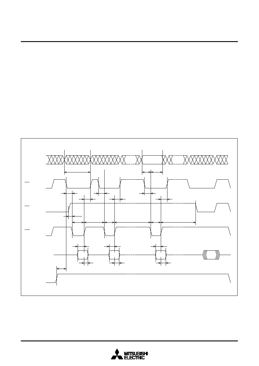
70
3886 Group
SINGLE-CHIP 8-BIT CMOS MICROCOMPUTER
MITSUBISHI MICROCOMPUTERS
q
Erase command
The erase command is executed by inputting command code 20
16
in the first cycle and command code 20
16
again in the second
cycle. The command code is latched into the internal command
___
latch at the rising edges of the WE input in the first cycle and in
the second cycle, respectively. The erase operation is initiated at
___
the rising edge of the WE input in the second cycle, and the
memory contents are collectively erased within 9.5 ms as mea-
sured by the internal timer. Note that data 00
16
must be written to
all memory locations before executing the erase command.
Note: An erase operation is not completed by executing the erase
command once. Always be sure to execute an erase verify
command after executing the erase command. When the fail-
ure is found in this verification, the user must repeatedly ex-
ecute the erase command until the pass. Refer to Figure 71
for the erase flowchart.
Fig. 70 Input/output timings during erasing (verify data is output at the same timing as for read.)
q
Erase verify command
The user must verify the contents of all addresses after complet-
ing the erase command. The microcomputer enters the erase
verify mode by inputting the verify address and command code
A0
16
in the first cycle. The address is internally latched at the fall-
___
ing edge of the WE input, and the command code is internally
___
latched at the rising edge of the WE input. When control signals
are input in the second cycle at the timing shown in Figure 70, the
M38869FFAHP/GP outputs the contents of the specified address
to the external.
Note: If any memory location where the contents have not been
erased is found in the erase verify operation, execute the op-
eration of "erase
erase verify" over again. In this case,
however, the user does not need to write data 00
16
to memory
locations before erasing.
Address
Erase
Erase verify
Verify
address
t
WC
t
CS
t
RRW
t
WP
t
WPH
t
WP
t
DE
t
DS
20
16
20
16
A0
16
Dout
t
DS
t
DH
t
DH
Verify data output
t
DH
t
VSC
t
DS
t
WP
t
WRR
t
CS
t
CS
t
CH
t
CH
t
CH
t
AS
t
AH
V
IH
V
IL
V
IH
V
IL
V
IH
V
IL
V
IH
V
IL
V
IH
V
IL
V
PP
H
V
PP
L
CE
OE
WE
Data
V
PP

71
3886 Group
SINGLE-CHIP 8-BIT CMOS MICROCOMPUTER
MITSUBISHI MICROCOMPUTERS
q
Reset command
The reset command provides a means of stopping execution of
the erase or program command safely. If the user inputs command
code FF
16
in the second cycle after inputting the erase or program
command in the first cycle and again input command code FF
16
in
the third cycle, the erase or program command is disabled (i.e.,
reset), and the M38869FFAHP/GP is placed in the read mode. If
the reset command is executed, the contents of the memory does
not change.
q
Device identification code command
By inputting command code 90
16
in the first cycle, the user can
read out the device identification code. The command code is
latched into the internal command latch at the rising edge of the
___
WE input. At this time, the user can read out manufacture's code
1C
16
(i.e., MITSUBISHI) by inputting 0000
16
to the address input
pins in the second cycle; the user can read out device code D0
16
(i. e., 1M-bit flash memory) by inputting 0001
16
.
These command and data codes are input/output at the same tim-
ing as for read.
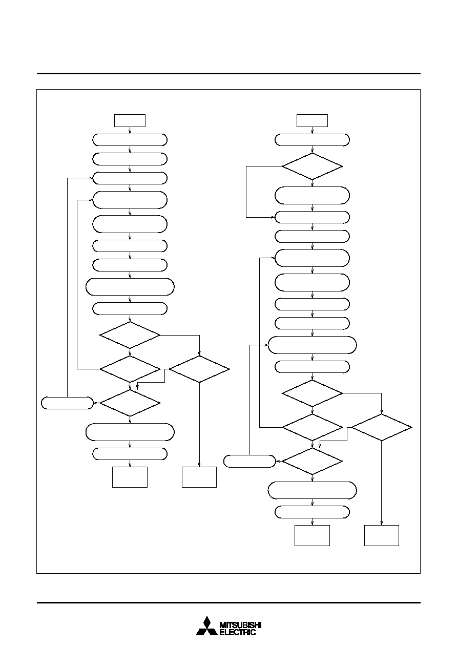
72
3886 Group
SINGLE-CHIP 8-BIT CMOS MICROCOMPUTER
MITSUBISHI MICROCOMPUTERS
Fig. 71 Programming/Erasing algorithm flow chart
START
V
CC
= 5 V, V
PP
= V
PP
H
ADRS = first location
X = 0
WRITE PROGRAM
COMMAND
WRITE PROGRAM
DATA
DURATION = 10
µ
s
X = X
+
1
WRITE PROGRAM-VERIFY
COMMAND
40
16
D
IN
C0
16
00
16
DURATION = 6
µ
s
X = 25 ?
LAST ADRS ?
NO
INC ADRS
WRITE READ COMMAND
V
PP
= V
PP
L
DEVICE
PASSED
DEVICE
FAILED
VERIFY BYTE ?
VERIFY BYTE ?
FAIL
FAIL
Program
Erase
YES
YES
NO
PASS
PASS
START
V
CC
= 5 V, V
PP
= V
PP
H
ADRS = first location
X = 0
WRITE ERASE
COMMAND
PROGRAM
ALL BYTES = 00
16
ALL
BYTES = 00
16
?
WRITE ERASE
COMMAND
DURATION = 9.5 ms
X = X
+
1
WRITE ERASE-VERIFY
COMMAND
20
16
20
16
A0
16
00
16
DURATION = 6
µ
s
X = 1000 ?
LAST ADRS ?
NO
INC ADRS
WRITE READ COMMAND
V
PP
= V
PP
L
DEVICE
PASSED
DEVICE
FAILED
VERIFY BYTE ?
VERIFY BYTE ?
FAIL
FAIL
YES
YES
NO
PASS
PASS
YES
NO
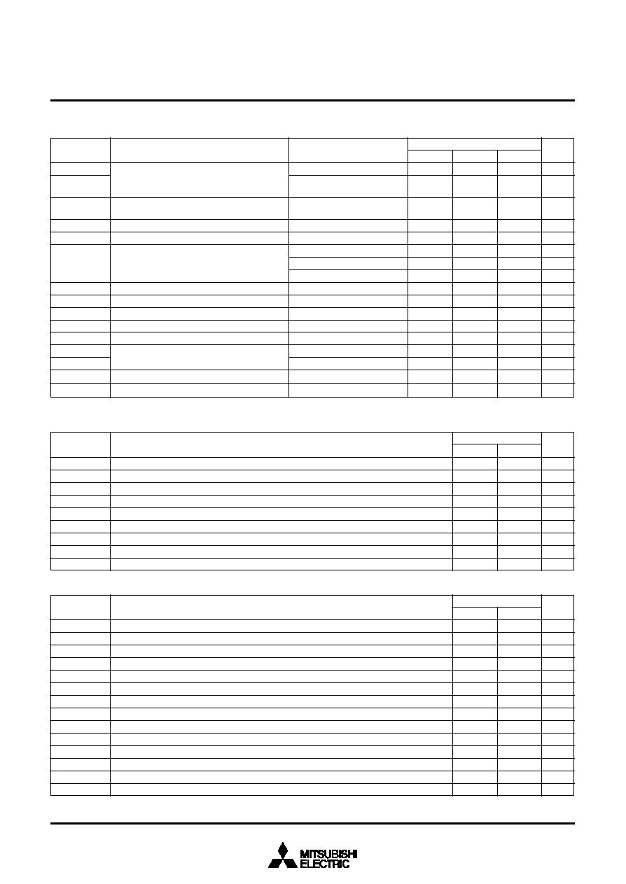
73
3886 Group
SINGLE-CHIP 8-BIT CMOS MICROCOMPUTER
MITSUBISHI MICROCOMPUTERS
Table 22 DC ELECTRICAL CHARACTERISTICS (T
a
= 25 ∞C, V
CC
= 5 V ± 10 %, unless otherwise noted)
Symbol
Max.
1
100
15
15
15
10
100
100
30
30
0.8
V
CC
0.45
V
CC
+ 1.0
12.6
__
V
CC
= 5.5 V, CE = V
IH
V
CC
= 5.5 V,
__
CE = V
CC
± 0.2 V
__
V
CC
= 5.5 V, CE = V
IL
,
t
RC
= 150 ns, I
OUT
= 0 mA
V
PP
= V
PP
H
V
PP
= V
PP
H
0
V
PP
V
CC
V
CC
<V
PP
V
CC
+ 1.0 V
V
PP
= V
PP
H
V
PP
= V
PP
H
V
PP
= V
PP
H
I
OL
= 2.1 mA
I
OH
= ≠400
µ
A
I
OH
= ≠100
µ
A
I
SB1
I
SB2
I
CC1
I
CC2
I
CC3
I
PP1
I
PP2
I
PP3
V
IL
V
IH
V
OL
V
OH1
V
OH2
V
PP
L
V
PP
H
V
CC
supply current (at standby)
V
CC
supply current (at read)
V
CC
supply current (at program)
V
CC
supply current (at erase)
V
PP
supply current (at read)
V
PP
supply current (at program)
V
PP
supply current (at erase)
"L" input voltage
"H" input voltage
"L" output voltage
"H" output voltage
V
PP
supply voltage (read only)
V
PP
supply voltage (read/write)
Parameter
Test conditions
Typ.
Min.
Limits
mA
µ
A
mA
mA
mA
µ
A
µ
A
µ
A
mA
mA
V
V
V
V
V
V
V
Unit
0
2.0
2.4
V
CC
≠0.4
V
CC
11.7
12.0
AC ELECTRICAL CHARACTERISTICS (T
a
= 25 ∞C, V
CC
= 5 V ± 10 %, unless otherwise noted)
Table 23 Read-only mode
Symbol
Max.
Parameter
Min.
Limits
Unit
t
RC
t
a(AD)
t
a(CE)
t
a(OE)
t
CLZ
t
OLZ
t
DF
t
DH
t
WRR
Read cycle time
Address access time
__
CE access time
__
OE access time
__
Output enable time (after CE)
__
Output enable time (after OE)
__
Output floating time (after OE)
__
__
Output valid time (after CE, OE, address)
Write recovery time (before read)
250
0
0
0
6
250
250
100
35
ns
ns
ns
ns
ns
ns
ns
ns
µ
s
Table 24 Read/Write mode
Symbol
Max.
Parameter
Min.
Limits
Unit
t
WC
t
AS
t
AH
t
DS
t
DH
t
WRR
t
RRW
t
CS
t
CH
t
WP
t
WPH
t
DP
t
DE
t
VSC
Write cycle time
Address set up time
Address hold time
Data setup time
Data hold time
Write recovery time (before read)
Read recovery time (before write)
__
CE setup time
__
CE hold time
Write pulse width
Write pulse waiting time
Program time
Erase time
V
PP
setup time
150
0
60
50
10
6
0
20
0
60
20
10
9.5
1
ns
ns
ns
ns
ns
µ
s
µ
s
ns
ns
ns
ns
µ
s
ms
µ
s
Note: Read timing of Read/Write mode is same as Read-only mode.
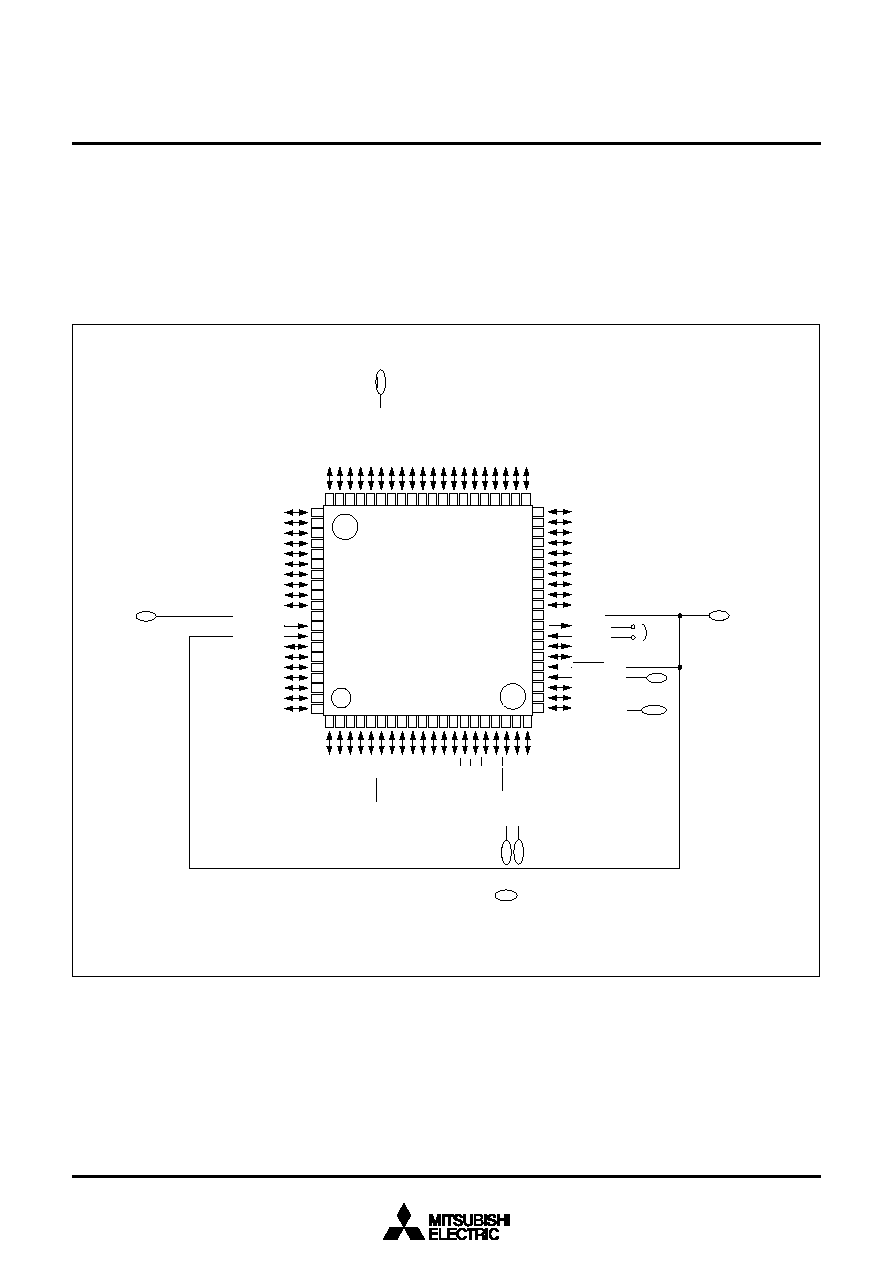
74
3886 Group
SINGLE-CHIP 8-BIT CMOS MICROCOMPUTER
MITSUBISHI MICROCOMPUTERS
(2) Flash memory mode 2 (serial I/O mode)
The M38869FFAHP/GP has a function to serially input/output the
software commands, addresses, and data required for operation
on the internal flash memory (e. g., read, program, and erase) us-
ing only a few pins. This is called the serial I/O (input/output)
mode. This mode can be selected by driving the SDA (serial data
__
input/output), SCLK (serial clock input ), and OE pins high after
connecting wires as shown in Figures 72 and powering on the V
CC
pin and then applying V
PP
H to the V
PP
pin.
In the serial I/O mode, the user can use six types of software com-
mands: read, program, program verify, erase, erase verify and
error check.
Serial input/output is accomplished synchronously with the clock,
beginning from the LSB (LSB first).
Fig. 72 Pin connection of M38869FFAHP/GP when operating in serial I/O mode
1
2
3
4
7
8 9 1
0 1
1 1
2 1
3 1
4 1
5 1
6 1
7 1
8 1
9 2
0
5
6
2
1
2
2
2
3
2
4
2
5
2
6
2
7
2
8
2
9
3
0
3
1
3
2
3
3
3
4
3
5
3
6
3
7
3
8
3
9
4
0
4
1
4
2
4
3
4
4
4
5
4
6
4
7
4
8
4
9
5
0
5
1
5
2
5
3
5
4
5
5
5
6
5
7
5
8
5
9
6
0
6
1
6
2
6
3
6
4
6
5
6
6
6
7
6
8
6
9
7
0
7
1
7
2
7
3
7
4
7
5
7
6
7
7
7
8
7
9
8
0
P
3
0
/
P
W
M
0
0
P
3
1
/
P
W
M
1
0
P
6
2
/
A
N
2
P
6
1
/
A
N
1
P
6
0
/
A
N
0
P
7
7
/
S
C
L
P
7
6
/
S
D
A
P
7
5
/
I
N
T
4
1
P
7
4
/
I
N
T
3
1
P
7
2
/
S
C
L
K
2
P
7
1
/
S
O
U
T
2
P
7
0
/
S
I
N
2
P
5
7
/
D
A
2
/
P
W
M
1
1
P
5
0
/
A
0
P
4
5
/
T
X
D
P
4
4
/
R
X
D
P
4
3
/
I
N
T
1
/
O
B
F
0
1
P
6
3
/
A
N
3
P
6
4
/
A
N
4
P
6
5
/
A
N
5
P
6
6
/
A
N
6
A
V
S
S
P
6
7
/
A
N
7
V
R
E
F
V
C
C
P
8
0
/
D
Q
0
P
8
1
/
D
Q
1
P
8
2
/
D
Q
2
P
8
3
/
D
Q
3
P
8
4
/
D
Q
4
P
8
5
/
D
Q
5
P
8
6
/
D
Q
6
P
8
7
/
D
Q
7
P
4
2
/
I
N
T
0
/
O
B
F
0
0
C
N
V
S
S
X
I
N
X
O
U
T
V
S
S
R
E
S
E
T
P
7
3
/
S
R
D
Y
2
/
I
N
T
2
1
P
5
5
/
C
N
T
R
1
P
5
4
/
C
N
T
R
0
P
5
6
/
D
A
1
/
P
W
M
0
1
P
4
0
/
X
C
O
U
T
P
4
1
/
X
C
I
N
P
4
7
/
S
R
D
Y
1
/
S
1
P
5
2
/
I
N
T
3
0
/
R
P
5
3
/
I
N
T
4
0
/
W
P
5
1
/
I
N
T
2
0
/
S
0
P
3
4
P
3
5
P
0
0
/
P
3
R
E
F
P
0
4
P
0
5
P
0
6
P
0
7
P
1
1
P
1
2
P
1
3
P
1
4
P
1
5
P
1
6
P
1
7
P
2
6
P
2
5
P
2
4
P
2
3
P
2
2
P
2
1
P
2
0
P
1
0
P
0
1
P
0
2
P
3
2
P
3
3
P
3
6
P
3
7
P
0
3
P
2
7
P
4
6
/
S
C
L
K
1
/
O
B
F
1
0
M
3
8
8
6
9
F
F
A
H
P
M
3
8
8
6
9
F
F
A
G
P
V
p
p
O
E
V
s
s
V
c
c
S
D
A
B
U
S
Y
S
C
L
K
*
:
C
o
n
n
e
c
t
t
o
t
h
e
c
e
r
a
m
i
c
o
s
c
i
l
l
a
t
i
o
n
c
i
r
c
u
i
t
.
i
n
d
i
c
a
t
e
s
t
h
e
f
l
a
s
h
m
e
m
o
r
y
p
i
n
.
*
75
3886 Group
SINGLE-CHIP 8-BIT CMOS MICROCOMPUTER
MITSUBISHI MICROCOMPUTERS
Table 25 Pin description (flash memory serial I/O mode)
V
CC
, V
SS
CNV
SS
_____
RESET
X
IN
X
OUT
AV
SS
V
REF
P0
0
≠P0
7
P1
0
≠P1
7
P2
0
≠P2
7
P3
0
≠P3
6
P3
7
P4
0
≠P4
3
,
P4
5
P4
4
P4
6
P4
7
P5
0
≠P5
7
P6
0
≠P6
7
P7
0
≠P7
7
P8
0
≠P8
7
Pin
Power supply
V
PP
input
Reset input
Clock input
Clock output
Analog supply input
Reference voltage input
Input port P0
Input port P1
Input port P2
Input port P3
Control signal input
Input port P4
SDA I/O
SCLK input
BUSY output
Input port P5
Input port P6
Input port P7
Input port P8
Name
--
Input
Input
Input
Output
--
Input
Input
Input
Input
Input
Input
Input
I/O
Input
Output
Input
Input
Input
Input
Input
/Output
Functions
Supply 5 V ± 10 % to V
CC
and 0 V to V
SS
.
Connect to 11.7 to 12.6 V.
Connect to V
SS
.
Connect a ceramic resonator between X
IN
and X
OUT
.
Connect to V
SS
.
Input an arbitrary level between the range of V
SS
and V
CC
.
Input "H" or "L", or keep them open.
Input "H" or "L", or keep them open.
Input "H" or "L", or keep them open.
Input "H" or "L", or keep them open.
__
OE input pin
Input "H" or "L" to P4
0
- P4
3
, P4
5
, or keep them open.
This pin is for serial data I/O.
This pin is for serial clock input.
This pin is for BUSY signal output.
Input "H" or "L", or keep them open.
Input "H" or "L", or keep them open.
Input "H" or "L", or keep them open.
Input "H" or "L", or keep them open.
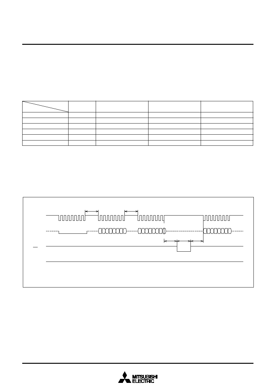
76
3886 Group
SINGLE-CHIP 8-BIT CMOS MICROCOMPUTER
MITSUBISHI MICROCOMPUTERS
Functional Outline (serial I/O mode)
In the serial I/O mode, data is transferred synchronously with the
clock using serial input/output. The input data is read from the
SDA pin into the internal circuit synchronously with the rising edge
of the serial clock pulse; the output data is output from the SDA
pin synchronously with the falling edge of the serial clock pulse.
Data is transferred in units of eight bits.
In the first transfer, the user inputs the command code. This is fol-
lowed by address input and data input/output according to the
contents of the command. Table 26 shows the software com-
mands used in the serial I/O mode. The following explains each
software command.
Table 26 Software command (serial I/O mode)
Read
Program
Program verify
Erase
Erase verify
Error check
Number of transfers
Command
First command
code input
00
16
40
16
C0
16
20
16
A0
16
80
16
Read address L (Input)
Program address L (Input)
Verify data (Output)
20
16
(Input)
Verify address L (Input)
Error code (Output)
Second
Read address H (Input)
Program address H (Input)
----------
----------
Verify address H (Input)
----------
Third
Fourth
Read data (Output)
Program data (Input)
----------
----------
Verify data (Output)
----------
q
Read command
Input command code 00
16
in the first transfer. Proceed and input
the low-order 8 bits and the high-order 8 bits of the address and
__
pull the OE pin low. When this is done, the M38869FFAHP/GP
reads out the contents of the specified address, and then latchs it
__
into the internal data latch. When the OE pin is released back high
and serial clock is input to the SCLK pin, the read data that has
been latched into the data latch is serially output from the SDA
pin.
Fig. 73 Timings during reading
"L"
SCLK
BUSY
OE
SDA
t
CH
A
0
A
7
A
8
A
15
D
0
D
7
t
CH
t
CR
Command code input (00
16
)
Read address input (L)
Read address input (H)
Read data output
t
WR
Read
t
RC
Note : When outputting the read data, the SDA pin is switched for output at the first falling edge of SCLK. The SDA pin is placed
in the floating state during the period of th
(C-E)
after the last rising edge of SCLK (at the 8th bit).
0 0 0 0 0 0 0 0
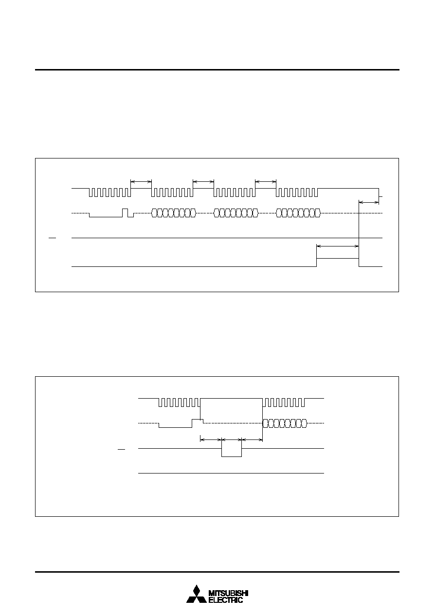
77
3886 Group
SINGLE-CHIP 8-BIT CMOS MICROCOMPUTER
MITSUBISHI MICROCOMPUTERS
q
Program command
Input command code 40
16
in the first transfer. Proceed and input
the low-order 8 bits and the high-order 8 bits of the address and
then program data. Programming is initiated at the last rising edge
of the serial clock during program data transfer. The BUSY pin is
driven high during program operation. Programming is completed
within 10
µ
s as measured by the internal timer, and the BUSY pin
is pulled low.
Note : A programming operation is not completed by executing the
program command once. Always be sure to execute a pro-
gram verify command after executing the program command.
When the failure is found in the verification, the user must re-
peatedly execute the program command until the pass in the
verification. Refer to Figure 71 for the programming flowchart.
q
Program verify command
Input command code C0
16
in the first transfer. Proceed and drive
__
the OE pin low. When this is done, The M38869FFAHP/GP verify-
reads the programmed address's contents, and then latchs it into
__
the internal data latch. When the OE pin is released back high and
serial clock is input to the SCLK pin, the verify data that has been
latched into the data latch is serially output from the SDA pin.
Fig. 75 Timings during program verify
Fig. 74 Timings during programming
SCLK
BUSY
OE
SDA
t
CH
A
0
0 0 0 0 0 0 1 0
A
7
A
8
A
15
D
0
D
7
t
CH
t
CH
t
PC
Command code input (40
16
)
Program address input (L)
Program address input (H)
Program data input
t
WP
Program
SCLK
BUSY
OE
SDA
D
0
D
7
t
CRPV
Command code input (C0
16
)
Verify data output
t
WR
Verify read
t
RC
Note: When outputting the verify data, the SDA pin is switched for output at the first falling edge of SCLK. The SDA pin is placed
in the floating state during the period of th
(C-E)
after the last rising edge of SCLK (at the 8th bit).
0 0 0 0 0 0 1 1
"L"
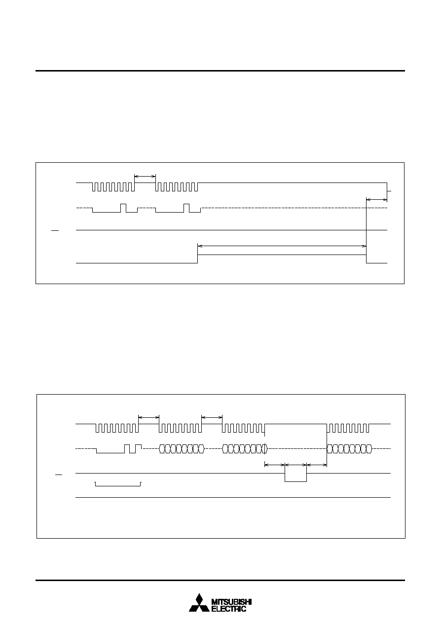
78
3886 Group
SINGLE-CHIP 8-BIT CMOS MICROCOMPUTER
MITSUBISHI MICROCOMPUTERS
q
Erase command
Input command code 20
16
in the first transfer and command code
20
16
again in the second transfer. When this is done, the
M38869FFAHP/GP executes an erase command. Erase is initi-
ated at the last rising edge of the serial clock. The BUSY pin is
driven high during the erase operation. Erase is completed within
9.5 ms as measured by the internal timer, and the BUSY pin is
pulled low. Note that data 00
16
must be written to all memory loca-
tions before executing the erase command.
Note: A erase operation is not completed by executing the erase
command once. Always be sure to execute a erase verify
command after executing the erase command. When the fail-
ure is found in the verification, the user must repeatedly ex-
ecute the erase command until the pass in the verification.
Refer to Figure 71 for the erase flowchart.
Fig. 76 Timings at erasing
q
Erase verify command
The user must verify the contents of all addresses after complet-
ing the erase command. Input command code A0
16
in the first
transfer. Proceed and input the low-order 8 bits and the high-order
__
8 bits of the address and pull the OE pin low. When this is done,
the M38869FFAHP/GP reads out the contents of the specified ad-
__
dress, and then latchs it into the internal data latch. When the OE
pin is released back high and serial clock is input to the SCLK pin,
the verify data that has been latched into the data latch is serially
output from the SDA pin.
Note: If any memory location where the contents have not been
erased is found in the erase verify operation, execute the op-
eration of "erase
erase verify" over again. In this case,
however, the user does not need to write data 00
16
to memory
locations before erasing.
Fig. 77 Timings during erase verify
tw
E
SCLK
BUSY
OE
SDA
t
CH
t
EC
0 0 0 0 0 1 0 0
0 0 0 0 0 1 0 0
Command code input (20
16
) Command code input (20
16
)
Erase
"H"
"L"
SCLK
BUSY
OE
SDA
t
CH
A
0
A
7
A
8
A
15
D
0
D
7
t
CH
t
CREV
Command code input (A0
16
) Verify address input (L)
Verify address input (H)
Verify data output
t
WR
Verify read
t
RC
Note : When outputting the verify data, the SDA pin is switched for output at the first falling edge of SCLK. The SDA pin is placed
in the floating state during the period of th
(C-E)
after the last rising edge of SCLK (at the 8th bit).
0 0 0 0 0 1 0 1
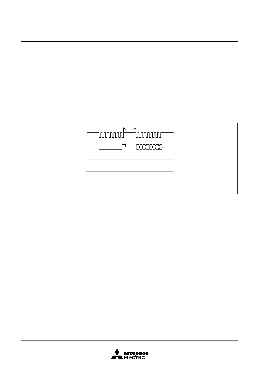
79
3886 Group
SINGLE-CHIP 8-BIT CMOS MICROCOMPUTER
MITSUBISHI MICROCOMPUTERS
q
Error check command
Input command code 80
16
in the first transfer, and the
M38869FFAHP/GP outputs error information from the SDA pin,
beginning at the next falling edge of the serial clock. If the LSB bit
of the 8-bit error information is 1, it indicates that a command error
has occurred. A command error means that some invalid com-
mands other than commands shown in Table 26 has been input.
When a command error occurs, the serial communication circuit
sets the corresponding flag and stops functioning to avoid an erro-
neous programming or erase. When being placed in this state, the
serial communication circuit does not accept the subsequent serial
clock and data (even including an error check command). There-
fore, if the user wants to execute an error check command,
temporarily drop the V
PP
pin input to the V
PP
L level to terminate
the serial input/output mode. Then, place the M38869FFAHP/GP
into the serial I/O mode back again. The serial communication cir-
cuit is reset by this operation and is ready to accept commands.
The error flag alone is not cleared by this operation, so the user
can examine the serial communication circuit's error conditions
before reset. This examination is done by the first execution of an
error check command after the reset. The error flag is cleared
when the user has executed the error check command. Because
the error flag is undefined immediately after power-on, always be
sure to execute the error check command.
Fig. 78 Timings at error checking
Note: The programming/erasing algorithm flow chart of the serial
I/O mode is the same as that of the parallel I/O mode. Re-
fer to Figure 71.
SCLK
BUSY
OE
SDA
E0
t
CH
Command code input (80
16
)
Error flag output
0 0 0 0 0 0 0 1
? ? ? ? ? ?
Note: When outputting the error flag, the SDA pin is switched for output at the first falling edge of the serial clock. The SDA pin is placed
in the floating state during the period of th
(C-E)
after the last rising edge of the serial clock (at the 8th bit).
?
"H"
"L"
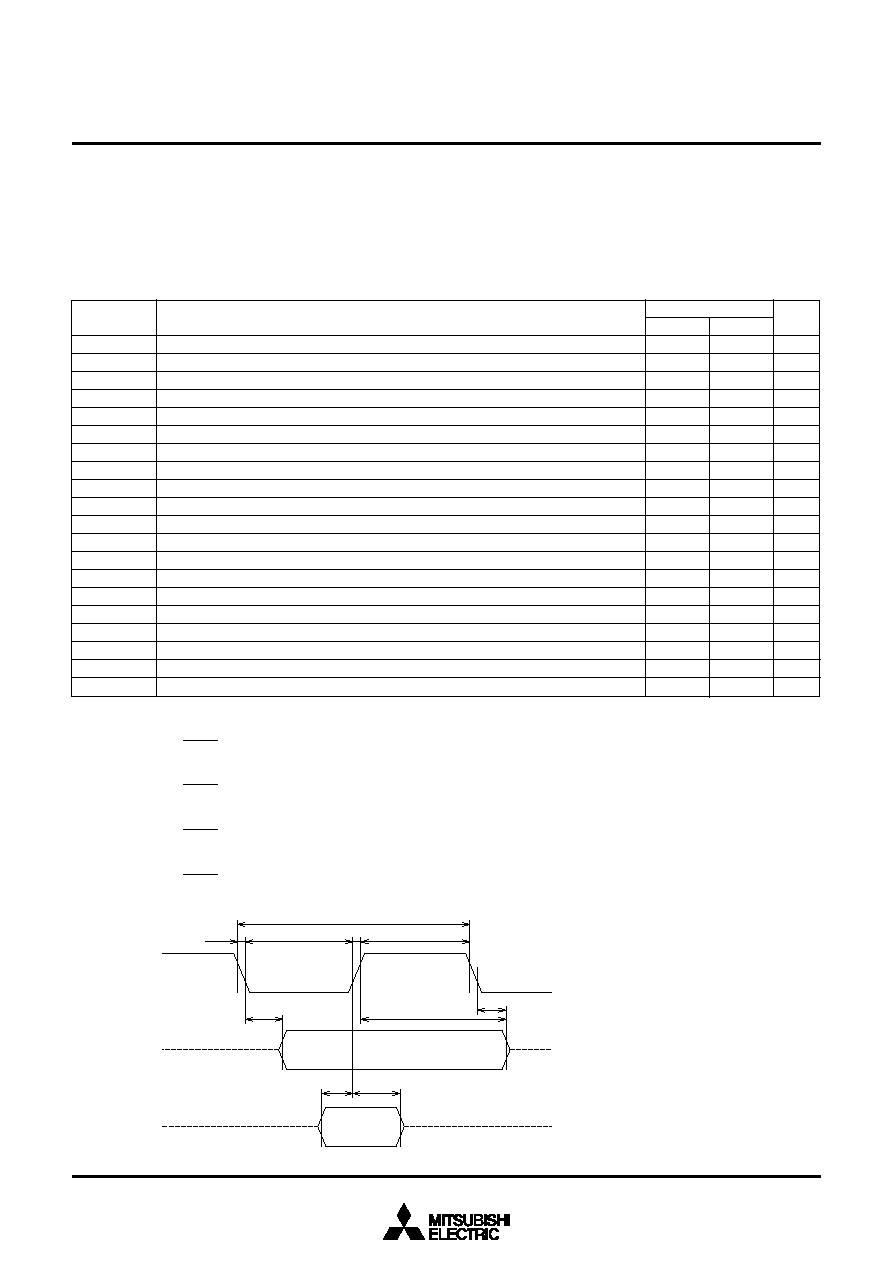
80
3886 Group
SINGLE-CHIP 8-BIT CMOS MICROCOMPUTER
MITSUBISHI MICROCOMPUTERS
DC ELECTRICAL CHARACTERISTICS
(Ta = 25 ∞C, V
CC
= 5 V ± 10 %, V
PP
= 11.7 to 12.6 V, unless otherwise noted)
I
CC
, I
PP
-relevant standards during read, program, and erase are the same as in the parallel input/output mode. V
IH
, V
IL
, V
OH
, V
OL
, I
IH
, and
__
I
IL
for the SCLK, SDA, BUSY, OE pins conform to the microcomputer modes.
Table 27 AC Electrical characteristics
(T
a
= 25 ∞C, V
CC
= 5 V ± 10 %, V
PP
= 11.7 to 12.6 V, f(X
IN
) = 10 MHz, unless otherwise noted)
Symbol
Max.
10
9.5
90
250
(Note 4)
t
CH
t
CR
t
WR
t
RC
t
CRPV
t
WP
t
PC
t
CREV
t
WE
t
EC
t
c(CK)
t
w(CKH)
t
w(CKL)
t
r(CK)
t
f(CK)
t
d(C-Q)
t
h(C-Q)
t
h(C-E)
t
su(D-C)
t
h(C-D)
Serial transmission interval
Read waiting time after transmission
Read pulse width
Transfer waiting time after read
Waiting time before program verify
Programming time
Transfer waiting time after programming
Waiting time before erase verify
Erase time
Transfer waiting time after erase
SCLK input cycle time
SCLK high-level pulse width
SCLK low-level pulse width
SCLK rise time
SCLK fall time
SDA output delay time
SDA output hold time
SDA output hold time (only the 8th bit)
SDA input set up time
SDA input hold time
Parameter
ns
ns
ns
ns
µ
s
µ
s
ns
ns
ns
ns
ns
ns
ns
ns
ns
ns
ns
ns
Unit
Min.
500
(Note 1)
500
(Note 1)
400
(Note 2)
500
(Note 1)
6
500
(Note 1)
6
500
(Note 1)
250
100
100
20
20
0
0
150
(Note 3)
30
90
Limits
Notes 1: When f(X
IN
) = 10 MHz or less, calculate the minimum value according to formula 1.
Formula 1 :
◊
10
6
2: When f(X
IN
) = 10 MHz or less, calculate the minimum value according to formula 2.
Formula 2 :
◊
10
6
3: When f(X
IN
) = 10 MHz or less, calculate the minimum value according to formula 3.
Formula 3 :
◊
10
6
4: When f(X
IN
) = 10 MHz or less, calculate the minimum value according to formula 4
Formula 4 :
◊
10
6
5000
f(X
IN
)
4000
f(X
IN
)
2500
f(X
IN
)
1500
f(X
IN
)
AC waveforms
SCLK
SDA input
Test conditions for AC characteristics
∑ Output timing voltage : V
OL
= 0.8 V, V
OH
= 2.0 V
∑ Input timing voltage : V
IL
= 0.2 V
CC
, V
IH
= 0.8 V
CC
SDA output
t
c(CK)
t
r(CK)
t
d(C-Q)
t
su(D-C)
t
h(C-D)
t
h(C-E)
t
h(C-Q)
t
f(CK)
t
w(CKL)
t
w(CKH)
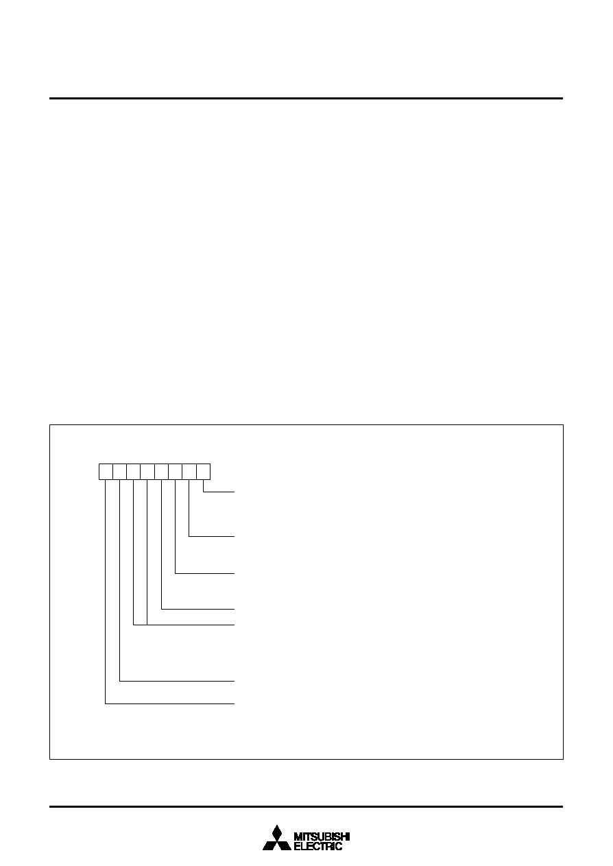
81
3886 Group
SINGLE-CHIP 8-BIT CMOS MICROCOMPUTER
MITSUBISHI MICROCOMPUTERS
(3) Flash memory mode 3 (CPU reprogramming
mode)
The M38869FFAHP/GP has the CPU reprogramming mode where
a built-in flash memory is handled by the central processing unit
(CPU).
In CPU reprogramming mode, the flash memory is handled by
writing and reading to/from the flash memory control register (see
Figure 79) and the flash command register (see Figure 80).
The CNV
SS
pin is used as the V
PP
power supply pin in CPU repro-
gramming mode. It is necessary to apply the power-supply voltage
of V
PP
H from the external to this pin.
Functional Outline (CPU reprogramming mode)
Figure 79 shows the flash memory control register bit configura-
t i o n . F i g u r e 8 0 s h o w s t h e f l a s h c o m m a n d r e g i s t e r b i t
configuration.
Bit 0 of the flash memory control register is the CPU reprogram-
ming mode select bit. When this bit is set to "1" and V
PP
H is
applied to the CNVss/V
PP
pin, the CPU reprogramming mode is
selected. Whether the CPU reprogramming mode is realized or
not is judged by reading the CPU reprogramming mode monitor
flag (bit 2 of the flash memory control register).
Bit 1 is a busy flag which becomes "1" during erase and program
execution.
Whether these operations have been completed or not is judged
by checking this flag after each command of erase and the pro-
gram is executed.
Bits 4, 5 of the flash memory control register are the erase/pro-
gram area select bits. These bits specify an area where erase and
program is operated. When the erase command is executed after
an area is specified by these bits, only the specified area is
erased. Only for the specified area, programming is enabled; for
the other areas, programming is disabled.
When CPU reprogramming mode is valid, the area where is not
specified by the erase/program area select bits cannot be read
out.
Transfer CPU reprogramming mode control program to internal
RAM before entering the CPU reprogramming mode, and then ex-
ecute this program on internal RAM.
If an interrupt occurs while this program is being executed, the
flash memory area is accessed, but normally operation cannot be
performed because the flash memory area cannot be read out.
During CPU reprogramming mode control program execution, ex-
ecute the processing such as interrupt disabled, etc.
Figure 81 shows the CPU mode register bit configuration in the
CPU reprogramming mode. Set bits 1 and 0 to "00" (single-chip
mode) in the CPU reprogramming mode.
Fig. 79 Flash memory control register bit configuration
7
6
5
4
3
2
1
0
0
0
Flash memory control regsiter
(FCON : address 0FFE16)
CPU reprogramming mode select bit (Note)
0 : CPU reprogramming mode is invalid. (Normal operation mode)
1 : When applying 0 V or VPPL to CNVSS/VPP pin, CPU reprogramming mode is
invalid. When applying VPPH to CNVSS/VPP pin, CPU reprogramming mode is valid.
Erase/Program busy flag
0 : Erase and program are completed or not have been executed.
1 : Erase/program is being executed.
CPU reprogramming mode monitor flag
0 : CPU reprogramming mode is invalid.
1 : CPU reprogramming mode is valid.
Erase/Program area select bits
0 0 : Addresses 100016 to FFFF16 (total 60 Kbytes)
0 1 : Addresses 100016 to 7FFF16 (total 28 Kbytes)
1 0 : Addresses 800016 to FFFF16 (total 32 Kbytes)
1 1 : Not available
Fix this bit to "0."
Fix this bit to "0."
Note: Bit 0 can be reprogrammed only when 0 V is applied to the CNVSS/VPP pin.
Not used (returns "0" when read)
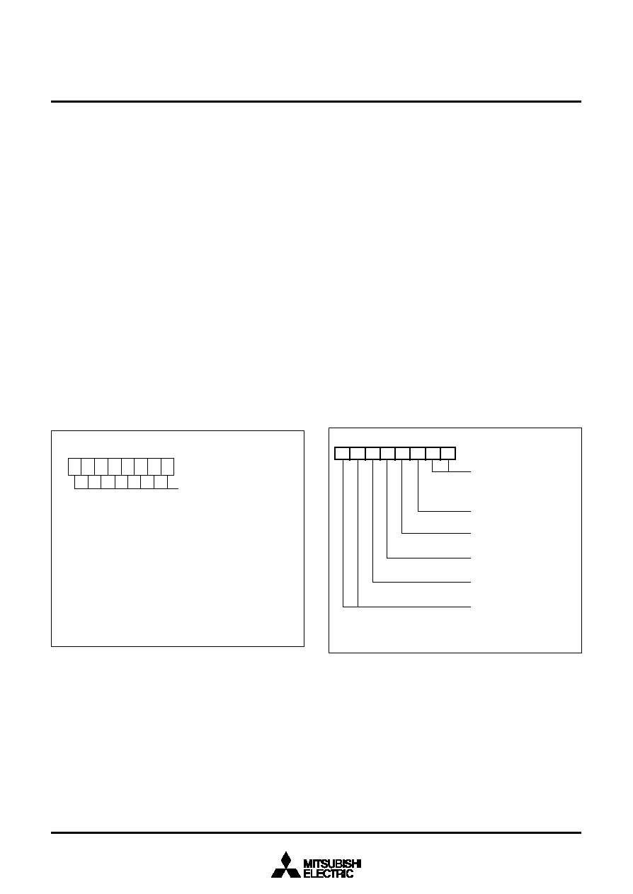
82
3886 Group
SINGLE-CHIP 8-BIT CMOS MICROCOMPUTER
MITSUBISHI MICROCOMPUTERS
q
CPU reprogramming mode operation procedure
The operation procedure in CPU reprogramming mode is de-
scribed below.
< Beginning procedure >
Apply 0 V to the CNVss/V
PP
pin for reset release.
After CPU reprogramming mode control program is transferred to
internal RAM, jump to this control program on RAM. (The follow-
ing operations are controlled by this control program).
Set "1" to the CPU reprogramming mode select bit.
Apply V
PP
H to the CNV
SS
/V
PP
pin.
Wait till CNV
SS
/V
PP
pin becomes 12 V.
Read the CPU reprogramming mode monitor flag to confirm
whether the CPU reprogramming mode is valid.
The operation of the flash memory is executed by software-com-
mand-writing to the flash command register .
Note: The following are necessary other than this:
∑Control for data which is input from the external (serial I/O
etc.) and to be programmed to the flash memory
∑Initial setting for ports etc.
∑Writing to the watchdog timer
< Release procedure >
Apply 0V to the CNV
SS
/V
PP
pin.
Wait till CNV
SS
/V
PP
pin becomes 0V.
Set the CPU reprogramming mode select bit to "0."
Each software command is explained as follows.
q
Read command
When "00
16
" is written to the flash command register, the
M38869FFAHP/GP enters the read mode. The contents of the
corresponding address can be read by reading the flash memory
(For instance, with the LDA instruction etc.) under this condition.
The read mode is maintained until another command code is written
to the flash command register. Accordingly, after setting the read
mode once, the contents of the flash memory can continuously be
read.
After reset and after the reset command is executed, the read
mode is set.
Fig. 80 Flash command register bit configuration
Fig. 81 CPU mode register bit configuration in CPU rewriting
mode
Writing of software command
<Command code>
"00
16
"
"40
16
"
"C0
16
"
"20
16
" + "20
16
"
"A0
16
"
"FF
16
" + "FF
16
"
<Software command name>
∑ Read command
∑ Program command
∑ Program verify command
∑ Erase command
∑ Erase verify command
∑ Reset command
Note: The flash command register is write-only register.
Flash command register
(FCMD : address 0FFF
16
)
7
6
5
4
3
2
1
0
C
P
U
m
o
d
e
r
e
g
i
s
t
e
r
(
C
P
U
M
:
a
d
d
r
e
s
s
0
0
3
B
1
6
)
b
7
b
0
S
t
a
c
k
p
a
g
e
s
e
l
e
c
t
i
o
n
b
i
t
0
:
0
p
a
g
e
1
:
1
p
a
g
e
R
e
s
e
r
v
e
d
(
D
o
n
o
t
w
r
i
t
e
"
0
"
t
o
t
h
i
s
b
i
t
w
h
e
n
u
s
i
n
g
X
C
I
N
≠
X
C
O
U
T
o
s
c
i
l
l
a
t
i
o
n
f
u
n
c
t
i
o
n
.
)
P
r
o
c
e
s
s
o
r
m
o
d
e
b
i
t
s
b
1
b
0
0
0
:
S
i
n
g
l
e
-
c
h
i
p
m
o
d
e
0
1
:
N
o
t
a
v
a
i
l
a
b
l
e
1
X
:
N
o
t
a
v
a
i
l
a
b
l
e
P
o
r
t
X
C
s
w
i
t
c
h
b
i
t
0
:
I
/
O
p
o
r
t
f
u
n
c
t
i
o
n
(
s
t
o
p
o
s
c
i
l
l
a
t
i
n
g
)
1
:
X
C
I
N
≠
X
C
O
U
T
o
s
c
i
l
l
a
t
i
n
g
f
u
n
c
t
i
o
n
M
a
i
n
c
l
o
c
k
(
X
I
N
≠
X
O
U
T
)
s
t
o
p
b
i
t
0
:
O
s
c
i
l
l
a
t
i
n
g
1
:
S
t
o
p
p
e
d
M
a
i
n
c
l
o
c
k
d
i
v
i
s
i
o
n
r
a
t
i
o
s
e
l
e
c
t
i
o
n
b
i
t
s
b
7
b
6
0
0
:
=
f
(
X
I
N
)
/
2
(
h
i
g
h
-
s
p
e
e
d
m
o
d
e
)
0
1
:
=
f
(
X
I
N
)
/
8
(
m
i
d
d
l
e
-
s
p
e
e
d
m
o
d
e
)
1
0
:
=
f
(
X
C
I
N
)
/
2
(
l
o
w
-
s
p
e
e
d
m
o
d
e
)
1
1
:
N
o
t
a
v
a
i
l
a
b
l
e
0
0

83
3886 Group
SINGLE-CHIP 8-BIT CMOS MICROCOMPUTER
MITSUBISHI MICROCOMPUTERS
q
Program command
When "40
16
" is written to the flash command register, the
M38869FFAHP/GP enters the program mode.
Subsequently to this, if the instruction (for instance, STA
instruction) for writing byte data in the address to be programmed
is executed, the control circuit of the flash memory executes the
program. The erase/program busy flag of the flash memory control
register is set to "1" when the program starts, and becomes "0"
when the program is completed. Accordingly, after the write in-
struction is executed, CPU can recognize the completion of the
program by polling this bit.
The programmed area must be specified beforehand by the erase/
program area select bits.
During programming, watchdog timer stops with "FFFF
16
" set.
Note: A programming operation is not completed by executing the
program command once. Always be sure to execute a pro-
gram verify command after executing the program command.
When the failure is found in this verification, the user must re-
peatedly execute the program command until the pass. Refer
to Figure 82 for the flow chart of the programming.
q
Program verify command
When "C0
16
" is written to the flash command register, the
M38869FFAHP/GP enters the program verify mode. Subsequently
to this, if the instruction (for instance, LDA instruction) for reading
byte data from the address to be verified (i.e., previously pro-
grammed address), the contents which has been written to the
address actually is read.
CPU compares this read data with data which has been written by
the previous program command. In consequence of the compari-
son, if not agreeing, the operation of "program
program verify"
must be executed again.
q
Erase command
When writing "20
16
" twice continuously to the flash command reg-
ister, the flash memory control circuit performs erase to the area
specified beforehand by the erase/program area select bits.
Erase/program busy flag of the flash memory control register be-
comes "1" when erase begins, and it becomes "0" when erase
completes. Accordingly, CPU can recognize the completion of
erase by polling this bit.
Data "00
16
" must be written to all areas to be erased by the pro-
gram and the program verify commands before the erase
command is executed.
During erasing, watchdog timer stops with "FFFF
16
" set.
Note: The erasing operation is not completed by executing the erase
command once. Always be sure to execute an erase verify
command after executing the erase command. When the fail-
ure is found in this verification, the user must repeatedly ex-
ecute the erase command until the pass. Refer to Figure 82 for
the erasing flowchart.
q
Erase verify command
When "A0
16
" is written to the flash command register, the
M38869FFAHP/GP enters the erase verify mode. Subsequently to
this, if the instruction (for instance, LDA instruction) for reading
byte data from the address to be verified, the contents of the ad-
dress is read.
CPU must erase and verify to all erased areas in a unit of ad-
dress.
If the address of which data is not "FF
16
" (i.e., data is not erased)
is found, it is necessary to discontinue erasure verification there,
and execute the operation of "erase
erase verify" again.
Note: By executing the operation of "erase
erase verify" again
when the memory not erased is found. It is unnecessary to
write data "00
16
" before erasing in this case.
q
Reset command
The reset command is a command to discontinue the program or
erase command on the way. When "FF
16
" is written to the command
register two times continuously after "40
16
" or "20
16
" is written to the
flash command register, the program, or erase command becomes
invalid (reset), and the M38869FFAHP/GP enters the reset mode.
The contents of the memory does not change even if the reset com-
mand is executed.
DC Electric Characteristics
Note: The characteristic concerning the flash memory part are the
same as the characteristic of the parallel I/O mode.
AC Electric Characteristics
Note: The characteristics are the same as the characteristic of the
microcomputer mode.
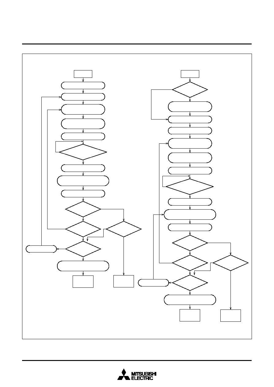
84
3886 Group
SINGLE-CHIP 8-BIT CMOS MICROCOMPUTER
MITSUBISHI MICROCOMPUTERS
Fig. 82 Flowchart of program/erase operation at CPU reprogramming mode
ERASE PROGRAM
BUSY FLAG = 0
START
ADRS = first location
X = 0
WRITE PROGRAM
COMMAND
WRITE PROGRAM
DATA
WAIT 1
µ
s
X = X
+
1
WRITE PROGRAM-VERIFY
COMMAND
40
16
DIN
C0
16
00
16
DURATION = 6
µ
s
X = 25 ?
LAST ADRS ?
NO
INC ADRS
WRITE READ COMMAND
DEVICE
PASSED
DEVICE
FAILED
VERIFY BYTE ?
VERIFY BYTE ?
FAIL
FAIL
Program
Erase
YES
YES
NO
PASS
PASS
START
ADRS = first location
X = 0
WRITE ERASE
COMMAND
PROGRAM
ALL BYTES = 00
16
ALL
BYTES = 00
16
?
WRITE ERASE
COMMAND
X = X
+
1
WRITE ERASE-VERIFY
COMMAND
20
16
20
16
A0
16
00
16
DURATION = 6
µ
s
X = 1000 ?
LAST ADRS ?
NO
INC ADRS
WRITE READ COMMAND
DEVICE
PASSED
DEVICE
FAILED
VERIFY BYTE ?
VERIFY BYTE ?
FAIL
FAIL
YES
YES
NO
PASS
PASS
YES
NO
ERASE PROGRAM
BUSY FLAG = 0
WAIT 1
µ
s
NO
YES
YES
NO

85
3886 Group
SINGLE-CHIP 8-BIT CMOS MICROCOMPUTER
MITSUBISHI MICROCOMPUTERS
NOTES ON PROGRAMMING
Processor Status Register
The contents of the processor status register (PS) after a reset are
undefined, except for the interrupt disable flag (I) which is "1." Af-
ter a reset, initialize flags which affect program execution. In
particular, it is essential to initialize the index X mode (T) and the
decimal mode (D) flags because of their effect on calculations.
Interrupts
The contents of the interrupt request bits do not change immedi-
ately after they have been written. After writing to an interrupt
request register, execute at least one instruction before perform-
ing a BBC or BBS instruction.
Decimal Calculations
∑ To calculate in decimal notation, set the decimal mode flag (D)
to "1", then execute an ADC or SBC instruction. After executing
an ADC or SBC instruction, execute at least one instruction be-
fore executing a SEC, CLC, or CLD instruction.
∑ In decimal mode, the values of the negative (N), overflow (V),
and zero (Z) flags are invalid.
Timers
If a value n (between 0 and 255) is written to a timer latch, the fre-
quency division ratio is 1/(n+1).
Multiplication and Division Instructions
∑ The index X mode (T) and the decimal mode (D) flags do not af-
fect the MUL and DIV instruction.
∑ The execution of these instructions does not change the con-
tents of the processor status register.
Ports
The contents of the port direction registers cannot be read. The
following cannot be used:
∑ The data transfer instruction (LDA, etc.)
∑ The operation instruction when the index X mode flag (T) is "1"
∑ The instruction with the addressing mode which uses the value
of a direction register as an index
∑ The bit-test instruction (BBC or BBS, etc.) to a direction register
∑ The read-modify-write instructions (ROR, CLB, or SEB, etc.) to
a direction register.
Use instructions such as LDM and STA, etc., to set the port direc-
tion registers.
Serial I/O
In clock synchronous serial I/O, if the receive side is using an ex-
ternal clock and it is to output the S
RDY1
signal, set the transmit
enable bit, the receive enable bit, and the S
RDY1
output enable bit
to "1."
Serial I/O1 continues to output the final bit from the T
X
D pin after
transmission is completed. S
OUT2
pin for serial I/O2 goes to high
impedance after transfer is completed.
When in serial I/O1 (clock-synchronous mode) or in serial I/O2, an
external clock is used as synchronous clock, write transmission
data to the transmit buffer register or serial I/O2 register, during
transfer clock is "H."
A-D Converter
The comparator uses capacitive coupling amplifier whose charge
will be lost if the clock frequency is too low.
Therefore, make sure that f(X
IN
) is at least on 500 kHz during an
A-D conversion.
Do not execute the STP or WIT instruction during an A-D conver-
sion.
D-A Converter
The accuracy of the D-A converter becomes rapidly poor under
the V
CC
= 4.0 V or less condition; a supply voltage of V
CC
4.0 V
is recommended. When a D-A converter is not used, set all values
of D-Ai conversion registers (i=1, 2) to "00
16
."
Instruction Execution Time
The instruction execution time is obtained by multiplying the pe-
riod of the internal clock
by the number of cycles needed to
execute an instruction.
The number of cycles required to execute an instruction is shown
in the list of machine instructions.
The period of the internal clock
is half of the X
IN
period in high-
speed mode.
When the ONW function is used in modes other than single-chip
mode, the period of the internal clock
may be four times that of
the X
IN
.

86
3886 Group
SINGLE-CHIP 8-BIT CMOS MICROCOMPUTER
MITSUBISHI MICROCOMPUTERS
NOTES ON USAGE
Handling of Power Source Pins
In order to avoid a latch-up occurrence, connect a capacitor suit-
able for high frequencies as bypass capacitor between power
source pin (V
CC
pin) and GND pin (V
SS
pin), between power
source pin (V
CC
pin) and analog power source input pin (AV
SS
pin), and between program power source pin (CNVss/V
PP
) and
GND pin for flash memory version when on-board reprogramming
is executed. Besides, connect the capacitor to as close as pos-
sible. For bypass capacitor which should not be located too far
from the pins to be connected, a ceramic capacitor of 0.01
µ
F≠0.1
µ
F is recommended.
EPROM version/One Time PROM version/
Flash memory version
The CNV
SS
pin is connected to the internal memory circuit block
by a low-ohmic resistance, since it has the multiplexed function to
be a programmable power source pin (V
PP
pin) as well.
To improve the noise reduction, connect a track between CNV
SS
pin and V
SS
pin or V
CC
pin with 1 to 10 k
resistance.
The mask ROM version track of CNV
SS
pin has no operational in-
terference even if it is connected to Vss pin or Vcc pin via a
resistor.
Erasing of Flash memory version
Set addresses 01000
16
to 0FFFF
16
as memory area for erasing in
the parallel serial I/O mode and the serial I/O mode. If the memory
area for erasing is set to mistaken area, the product may be per-
manently damaged.
DATA REQUIRED FOR MASK ORDERS
The following are necessary when ordering a mask ROM produc-
tion:
1.Mask ROM Confirmation Form
2.Mark Specification Form
3.Data to be written to ROM, in EPROM form (three identical cop-
ies)
DATA REQUIRED FOR One Time PROM
PROGRAMMING ORDERS
The following are necessary when ordering a PROM programming
service:
1.ROM Programming Confirmation Form
2.Mark Specification Form
3.Data to be programmed to PROM, in EPROM form (three identi-
cal copies)
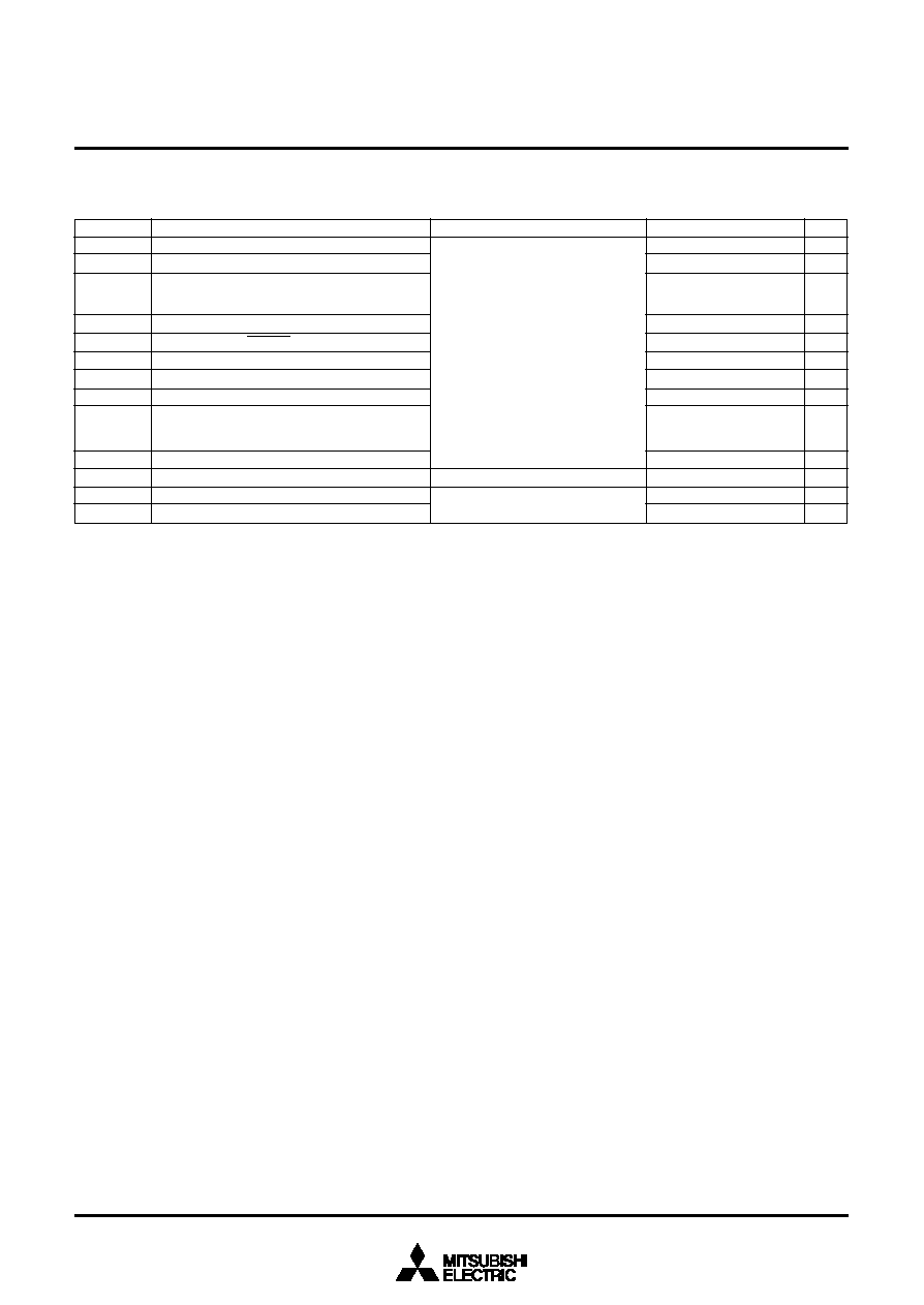
87
3886 Group
SINGLE-CHIP 8-BIT CMOS MICROCOMPUTER
MITSUBISHI MICROCOMPUTERS
ELECTRICAL CHARACTERISTICS
Table 28 Absolute maximum ratings
Power source voltage
S
(Note 1)
Power source voltage
S
(Note 2)
Input voltage
P0
0
≠P0
7
, P1
0
≠P1
7
, P2
0
≠P2
7
,
P3
0
≠P3
7
, P4
0
≠P4
7
, P5
0
≠P5
7
,
P6
0
≠P6
7
, P8
0
≠P8
7
, V
REF
Input voltage
P7
0
≠P7
7
Input voltage
RESET, X
IN
Input voltage
CNV
SS
(Note 3)
Input voltage
CNV
SS
(Note 4)
Input voltage
CNV
SS
(Note 5)
Output voltage P0
0
≠P0
7
, P1
0
≠P1
7
, P2
0
≠P2
7
,
P3
0
≠P3
7
, P4
0
≠P4
7
, P5
0
≠P5
7
,
P6
0
≠P6
7
, P8
0
≠P8
7
, X
OUT
Output voltage P7
0
≠P7
7
Power dissipation
Operating temperature
Storage temperature
V
CC
V
CC
V
I
V
I
V
I
V
I
V
I
V
I
V
O
V
O
P
d
T
opr
T
stg
Symbol
Parameter
Conditions
Ratings
≠0.3 to 7.0
≠0.3 to 6.5
≠0.3 to V
CC
+0.3
≠0.3 to 5.8
≠0.3 to V
CC
+0.3
≠0.3 to 7
≠0.3 to V
CC
+0.3
≠0.3 to 13
≠0.3 to V
CC
+0.3
≠0.3 to 5.8
500
≠20 to 85
≠40 to 125
V
V
V
V
V
V
V
V
V
V
mW
∞C
∞C
Unit
T
a
= 25 ∞C
All voltages are based on V
SS
.
Output transistors are cut off.
Notes 1: M38867M8A, M38867E8A
2: M38869M8A, M38869MCA, M38869MFA, M38869FFA
3: M38867M8A
4: M38869M8A, M38869MCA, M38869MFA
5: M38867E8A, M38869FFA

88
3886 Group
SINGLE-CHIP 8-BIT CMOS MICROCOMPUTER
MITSUBISHI MICROCOMPUTERS
5.5
5.5
5.5
V
CC
V
CC
V
CC
V
CC
5.5
5.5
5.5
V
CC
5.5
V
CC
5.5
V
CC
0.2V
CC
0.3V
CC
0.6
0.2V
CC
0.8
0.2V
CC
0.16V
CC
f(X
IN
)
4.1 MHz
f(X
IN
)
=
10 MHz
Power source voltage (flash memory version)
Power source voltage
when A-D converter is used
when D-A converter is used
Analog power source voltage
A-D converter input voltage
AN
0
≠AN
7
"H" input voltage
P0
0
≠P0
7
, P1
0
≠P1
7
, P2
0
≠P2
7
, P3
0
≠P3
7
, P4
0
, P4
1
,
P4
7
, P5
0
≠P5
7
, P6
0
≠P6
7
, P8
0
≠P8
7
"H" input voltage
P7
6
, P7
7
"H" input voltage (when I
2
C-BUS input level is selected)
S
DA
, S
CL
"H" input voltage (when SMBUS input level is selected)
S
DA
, S
CL
"H" input voltage (when CMOS input level is selected)
P4
2
≠P4
6
, DQ
0
≠DQ
7
, W, R, S
0
, S
1
, A
0
"H" input voltage (when CMOS input level is selected)
P7
0
≠P7
5
"H" input voltage (when TTL input level is selected)
P4
2
≠P4
6
, DQ
0
≠DQ
7
, W, R, S
0
, S
1
, A
0
(Note)
"H" input voltage (when TTL input level is selected)
P7
0
≠P7
5
(Note)
"H" input voltage
RESET, X
IN
, X
CIN
, CNV
SS
"L" input voltage
P0
0
≠P0
7
, P1
0
≠P1
7
, P2
0
≠P2
7
, P3
0
≠P3
7
, P4
0
≠P4
7
,
P5
0
≠P5
7
, P6
0
≠P6
7
, P7
0
≠P7
7,
P8
0
≠P8
7
"L" input voltage (when I
2
C-BUS input level is selected)
S
DA
, S
CL
"L" input voltage (when SMBUS input level is selected)
S
DA
, S
CL
"L" input voltage (when CMOS input level is selected)
P4
2
≠P4
6
, P7
0
≠P7
5
, DQ
0
≠DQ
7
, W, R, S
0
, S
1
, A
0
"L" input voltage (when TTL input level is selected)
P4
2
≠P4
6
, P7
0
≠P7
5
, DQ
0
≠DQ
7
, W, R, S
0
, S
1
, A
0
(Note)
"L" input voltage
RESET, CNV
SS
"L" input voltage
X
IN
, X
CIN
V
CC
V
CC
V
SS
V
REF
AV
SS
V
IA
V
IH
V
IH
V
IH
V
IH
V
IH
V
IH
V
IH
V
IH
V
IH
V
IL
V
IL
V
IL
V
IL
V
IL
V
IL
V
IL
Symbol
Parameter
Limits
Min.
V
V
V
V
V
V
V
V
V
V
V
V
V
V
V
V
V
V
V
V
V
V
Unit
Table 29 Recommended operating conditions
(V
CC
= 2.7 to 5.5 V, V
CC
= 4.0 to 5.5 V for flash memory version, T
a
= ≠20 to 85 ∞C, unless otherwise noted)
2.7
4.0
4.0
2.0
2.7
AV
SS
0.8V
CC
0.8V
CC
0.7V
CC
1.4
0.8V
CC
0.8V
CC
2.0
2.0
0.8V
CC
0
0
0
0
0
0
0
5.0
5.0
5.0
0
0
Typ.
Max.
Note : When V
CC
is 4.0 to 5.5 V.
Power source voltage (except flash memory version)
Analog reference voltage
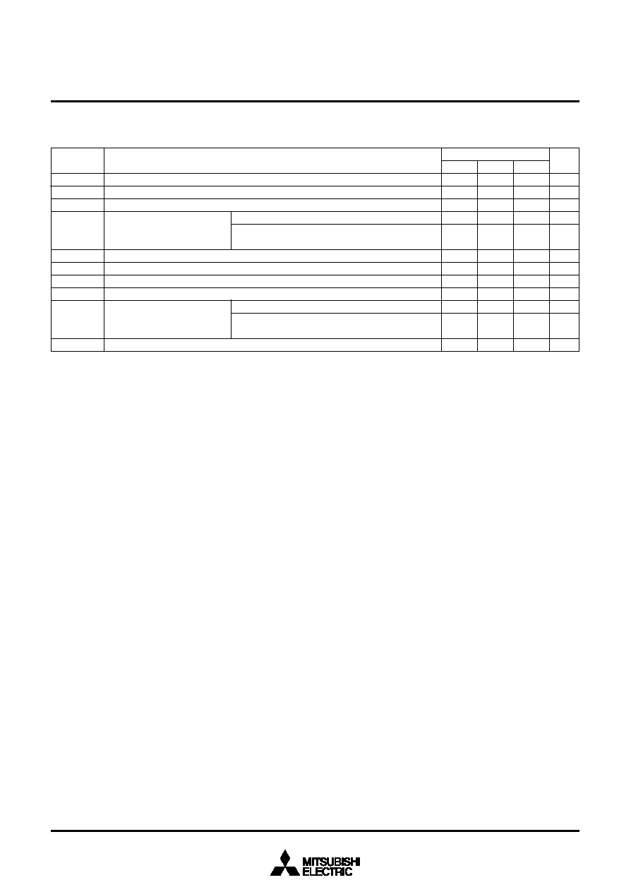
89
3886 Group
SINGLE-CHIP 8-BIT CMOS MICROCOMPUTER
MITSUBISHI MICROCOMPUTERS
Table 30 Recommended operating conditions
(V
CC
= 2.7 to 5.5 V, V
CC
= 4.0 to 5.5 V for flash memory version, T
a
= ≠20 to 85 ∞C, unless otherwise noted)
≠80
≠80
80
80
40
80
≠40
≠40
40
40
40
40
"H" total peak output current
P0
0
≠P0
7
, P1
0
≠P1
7
, P2
0
≠P2
7
, P3
0
≠P3
7
, P8
0
≠P8
7
(Note)
"H" total peak output current
P4
0
≠P4
7
, P5
0
≠P5
7
, P6
0
≠P6
7
(Note)
"L" total peak output current
P0
0
≠P0
7
, P1
0
≠P1
7
, P2
0
≠P2
3
, P3
0
≠P3
7
, P8
0
≠P8
7
(Note)
I
OH(peak)
I
OH(peak)
I
OL(peak)
I
OL(peak)
I
OL(peak)
I
OH(avg)
I
OH(avg)
I
OL(avg)
I
OL(avg)
I
OL(avg)
Symbol
Parameter
Limits
Min.
mA
mA
mA
mA
mA
mA
mA
mA
mA
mA
mA
mA
Unit
Typ.
Max.
In single-chip mode
Note : The total output current is the sum of all the currents flowing through all the applicable ports. The total average current is an average value measured
over 100 ms. The total peak current is the peak value of all the currents.
"L" total peak output current
P2
4
≠P2
7
(Note)
"L" total peak output current
P4
0
≠P4
7
,P5
0
≠P5
7
, P6
0
≠P6
7
, P7
0
≠P7
7
(Note)
"H" total average output current P0
0
≠P0
7
, P1
0
≠P1
7
, P2
0
≠P2
7
, P3
0
≠P3
7
, P8
0
≠P8
7
(Note)
"H" total average output current P4
0
≠P4
7
,P5
0
≠P5
7
, P6
0
≠P6
7
(Note)
"L" total average output current P0
0
≠P0
7
, P1
0
≠P1
7
, P2
0
≠P2
3
, P3
0
≠P3
7
, P8
0
≠P8
7
(Note)
"L" total average output current
P2
4
≠P2
7
(Note)
"L" total average output current P4
0
≠P4
7
,P5
0
≠P5
7
, P6
0
≠P6
7
, P7
0
≠P7
7
(Note)
In memory expansion mode
In microprocessor mode
In single-chip mode
In memory expansion mode
In microprocessor mode

90
3886 Group
SINGLE-CHIP 8-BIT CMOS MICROCOMPUTER
MITSUBISHI MICROCOMPUTERS
Table 31 Recommended operating conditions
(V
CC
= 2.7 to 5.5 V, V
CC
= 4.0 to 5.5 V for flash memory version, T
a
= ≠20 to 85 ∞C, unless otherwise noted)
≠10
10
20
10
≠5
5
15
5
10
4.5 V
CC
≠8
10
10
4.5 V
CC
≠8
50
"H" peak output current
P0
0
≠P0
7
, P1
0
≠P1
7
, P2
0
≠P2
7
, P3
0
≠P3
7
, P4
0
≠P4
7
,
P5
0
≠P5
7
, P6
0
≠P6
7
, P8
0
≠P8
7
(Note 1)
"L" peak output current
P0
0
≠P0
7
, P1
0
≠P1
7
, P2
0
≠P2
3
, P3
0
≠P3
7
, P4
0
≠P4
7
,
P5
0
≠P5
7
, P6
0
≠P6
7
, P7
0
≠P7
7
, P8
0
≠P8
7
(Note 1)
I
OH(peak)
I
OL(peak)
I
OL(peak)
I
OH(avg)
I
OL(avg)
I
OL(avg)
f(X
IN
)
Symbol
Parameter
Limits
Min.
mA
mA
mA
mA
mA
mA
mA
mA
MHz
MHz
MHz
MHz
MHz
kHz
Unit
Typ.
Max.
In single-chip mode
Notes 1: The peak output current is the peak current flowing in each port.
2: The average output current I
OL
(avg), I
OH
(avg) are average value measured over 100 ms.
3: When the oscillation frequency has a duty cycle of 50%.
4: When using the microcomputer in low-speed mode, set the sub-clock input oscillation frequency on condition that f(X
CIN
) < f(X
IN
)/3.
5: When using the timer X/Y, timer 1/2, serial I/O1, serial I/O2, A-D converter, comparator, and PWM, set the main clock input oscillation frequency to
the max. 4.5V
CC
≠8 (MHz).
In single-chip mode
In memory expansion mode
In microprocessor mode
In memory expansion mode
In microprocessor mode
32.768
f(X
CIN
)
"L" peak output current
P2
4
≠P2
7
(Note 1)
"H" average output current
P0
0
≠P0
7
, P1
0
≠P1
7
, P2
0
≠P2
7
, P3
0
≠P3
7
, P4
0
≠P4
7
,
P5
0
≠P5
7
, P6
0
≠P6
7
, P8
0
≠P8
7
(Note 2)
"L" average output current
P0
0
≠P0
7
, P1
0
≠P1
7
, P2
0
≠P2
3
, P3
0
≠P3
7
, P4
0
≠P4
7
,
P5
0
≠P5
7
, P6
0
≠P6
7
, P7
0
≠P7
7
, P8
0
≠P8
7
(Note 2)
"L" peak output current
P2
4
≠P2
7
(Note 2)
Main clock input oscillation
frequency (Note 3)
Sub-clock input oscillation frequency (Notes 3, 4)
High-speed mode
4.0 V
V
CC
5.5 V
High-speed mode
2.7 V
V
CC
4.0 V
Middle-speed mode
4.0 V
V
CC
5.5 V
Middle-speed mode
2.7 V
V
CC
4.0 V (Note 5)
Middle-speed mode
2.7 V
V
CC
4.0 V (Note 5)
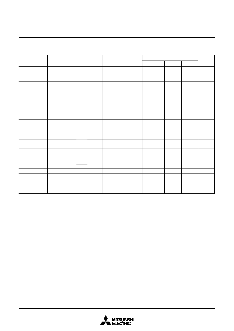
91
3886 Group
SINGLE-CHIP 8-BIT CMOS MICROCOMPUTER
MITSUBISHI MICROCOMPUTERS
Table 32 Electrical characteristics
(V
CC
= 2.7 to 5.5 V, V
CC
= 4.0 to 5.5 V for flash memory version, V
SS
= 0 V, T
a
= ≠20 to 85 ∞C, unless otherwise noted)
"H" output voltage
P0
0
≠P0
7
, P1
0
≠P1
7
, P2
0
≠P2
7
P3
0
≠P3
7
, P4
0
≠P4
7
, P5
0
≠P5
7
P6
0
≠P6
7
, P8
0
≠P8
7
(Note)
"L" output voltage
P0
0
≠P0
7
, P1
0
≠P1
7
, P2
0
≠P2
7
P3
0
≠P3
7
, P4
0
≠P4
7
, P5
0
≠P5
7
P6
0
≠P6
7
, P7
0
≠P7
7
, P8
0
≠P8
7
Hysteresis
CNTR
0
, CNTR
1
, INT
0
, INT
1
INT
20
≠INT
40
, INT
21
≠INT
41
P3
0
≠P3
7
Hysteresis
RxD, S
CLK1
, S
IN2
, S
CLK2
Hysteresis
RESET
"H" input current
P0
0
≠P0
7
, P1
0
≠P1
7
, P2
0
≠P2
7
P3
0
≠P3
7
, P4
0
≠P4
7
, P5
0
≠P5
7
P6
0
≠P6
7
, P7
0
≠P7
7
, P8
0
≠P8
7
"H" input current
RESET, CNV
SS
"H" input current
X
IN
"L" input current
P0
0
≠P0
7
, P1
0
≠P1
7
, P2
0
≠P2
7
P3
0
≠P3
7
, P4
0
≠P4
7
, P5
0
≠P5
7
P6
0
≠P6
7
, P7
0
≠P7
7
, P8
0
≠P8
7
"L" input current
RESET,CNV
SS
"L" input current
X
IN
"L" input current
P3
0
≠P3
7
(at Pull-up)
RAM hold voltage
Limits
V
V
V
V
V
V
V
µ
A
µ
A
µ
A
µ
A
µ
A
µ
A
µ
A
µ
A
V
Parameter
Min.
Typ.
Max.
Symbol
Unit
Note: P0
0
≠P0
3
are measured when the P0
0
≠P0
3
output structure selection bit of the port control register 1 (bit 0 of address 002E
16
) is "0".
P0
4
≠P0
7
are measured when the P0
4
≠P0
7
output structure selection bit of the port control register 1 (bit 1 of address 002E
16
) is "0".
P1
0
≠P1
3
are measured when the P1
0
≠P1
3
output structure selection bit of the port control register 1 (bit 2 of address 002E
16
) is "0".
P1
4
≠P1
7
are measured when the P1
4
≠P1
7
output structure selection bit of the port control register 1 (bit 3 of address 002E
16
) is "0".
P4
2
, P4
3
, P4
4
, and P4
6
are measured when the P4 output structure selection bit of the port control register 2 (bit 2 of address 002F
16
) is "0".
P4
5
is measured when the P4
5
/T
X
D P-channel output disable bit of the UART control register (bit 4 of address 001B
16
) is "0".
I
OH
= ≠10 mA
V
CC
= 4.0≠5.5 V
I
OH
= ≠1.0 mA
V
CC
= 2.7≠5.5 V
I
OL
= 10 mA
V
CC
= 4.0≠5.5 V
I
OL
= 1.6 mA
V
CC
= 2.7≠5.5 V
V
I
= V
CC
(Pin floating. Pull-up
transistors "off")
V
I
= V
CC
V
I
= V
CC
V
I
= V
SS
(Pin floating. Pull-up
transistors "off")
V
I
= V
SS
V
I
= V
SS
V
I
= V
SS
V
CC
= 4.0≠5.5 V
V
I
= V
SS
V
CC
= 2.7≠5.5 V
When clock stopped
V
CC
≠2.0
V
CC
≠1.0
≠20
≠10
2.0
Test conditions
0.4
0.5
0.5
4
≠4
≠60
2.0
0.4
5.0
5.0
≠5.0
≠5.0
≠120
5.5
V
OH
V
OL
V
T+
≠V
T≠
V
T+
≠V
T≠
V
T+
≠V
T≠
I
IH
I
IH
I
IH
I
IL
I
IL
I
IL
I
IL
V
RAM

92
3886 Group
SINGLE-CHIP 8-BIT CMOS MICROCOMPUTER
MITSUBISHI MICROCOMPUTERS
Table 33 Electrical characteristics
(V
CC
= 2.7 to 5.5 V, V
CC
= 4.0 to 5.5 V for flash memory version, V
SS
= 0 V, T
a
= ≠20 to 85 ∞C, unless otherwise noted)
Power source current
Limits
Parameter
Min.
Typ.
Max.
Symbol
Unit
High-speed mode
f(X
IN
) = 10 MHz
f(X
CIN
) = 32.768 kHz
Output transistors "off"
High-speed mode
f(X
IN
) = 8 MHz
f(X
CIN
) = 32.768 kHz
Output transistors "off"
High-speed mode
f(X
IN
) = 10 MHz (in WIT state)
f(X
CIN
) = 32.768 kHz
Output transistors "off"
Low-speed mode
f(X
IN
) = stopped
f(X
CIN
) = 32.768 kHz
Output transistors "off"
Low-speed mode
f(X
IN
) = stopped
f(X
CIN
) = 32.768 kHz (in WIT state)
Output transistors "off"
Low-speed mode (V
CC
= 3 V)
f(X
IN
) = stopped
f(X
CIN
) = 32.768 kHz
Output transistors "off"
Low-speed mode (V
CC
= 3 V)
f(X
IN
) = stopped
f(X
CIN
) = 32.768 kHz (in WIT state)
Output transistors "off"
Middle-speed mode
f(X
IN
) = 10 MHz
f(X
CIN
) = stopped
Output transistors "off"
Middle-speed mode
f(X
IN
) = 10 MHz (in WIT state)
f(X
CIN
) = stopped
Output transistors "off"
Increment when A-D conversion is
executed
f(X
IN
) = 10 MHz
All oscillation stopped
(in STP state)
Output transistors "off"
Test conditions
15
13
200
40
55
20.0
7.0
1.0
10
I
CC
Ta = 25 ∞C
Ta = 85 ∞C
8.0
6.8
1.6
60
20
20
8.0
4.0
1.5
800
0.1
mA
mA
mA
µ
A
µ
A
µ
A
µ
A
mA
mA
µ
A
µ
A
µ
A

93
3886 Group
SINGLE-CHIP 8-BIT CMOS MICROCOMPUTER
MITSUBISHI MICROCOMPUTERS
bit
LSB
2tc(X
IN
)
k
µ
A
µ
A
µ
A
Resolution
Absolute accuracy (excluding quantization error)
Conversion time
Ladder resistor
Reference power
source input current
A-D port input current
Min.
12
50
Typ.
35
150
Max.
10
±4
61
100
200
5
5.0
V
CC
= V
REF
= 5.0 V
V
REF
= 5.0 V
V
REF
= 5.0 V
Table 34 A-D converter characteristics (1)
(V
CC
= 2.7 to 5.5 V, V
CC
= 4.0 to 5.5 V for flash memory version, V
REF
= 2.0 V to V
CC
, V
SS
= AV
SS
= 0 V, T
a
= ≠20 to 85 ∞C, unless
otherwise noted)
10-bit A-D mode (when conversion mode selection bit (bit 7 of address 0038
16
) is "0")
Unit
Limits
Parameter
≠
≠
t
CONV
R
LADDER
I
VREF
I
I(AD)
Test conditions
at A-D converter operated
at A-D converter stopped
Note 1: Using one D-A converter, with the value in the D-A conversion register of the other D-A converter being "00
16
".
Table 37 Comparator characteristics
(V
CC
= 2.7 to 5.5 V, V
CC
= 4.0 to 5.5 V for flash memory version, V
SS
= 0 V, T
a
= ≠20 to 85 ∞C, unless otherwise noted)
Table 35 A-D converter characteristics (2)
(V
CC
= 2.7 to 5.5 V, V
CC
= 4.0 to 5.5 V for flash memory version, V
REF
= 2.0 V to V
CC
, V
SS
= AV
SS
= 0 V, T
a
= ≠20 to 85 ∞C, unless
otherwise noted)
8-bit A-D mode (when conversion mode selection bit (bit 7 of address 0038
16
) is "1")
Table 36 D-A converter characteristics
(V
CC
= 2.7 to 5.5 V, V
CC
= 4.0 to 5.5 V for flash memory version, V
REF
= 2.7 V to V
CC
, V
SS
= AV
SS
= 0 V, T
a
= ≠20 to 85 ∞C, unless
otherwise noted)
Symbol
bit
LSB
2tc(X
IN
)
k
µ
A
µ
A
µ
A
Resolution
Absolute accuracy (excluding quantization error)
Conversion time
Ladder resistor
Reference power
source input current
A-D port input current
Min.
12
50
Typ.
35
150
Max.
8
±2
50
100
200
5
5.0
V
CC
= V
REF
= 5.0 V
V
REF
= 5.0 V
V
REF
= 5.0 V
Unit
Limits
Parameter
≠
≠
t
CONV
R
LADDER
I
VREF
I
I(AD)
Test conditions
at A-D converter operated
at A-D converter stopped
Symbol
Bits
%
%
µ
s
k
mA
Resolution
Absolute accuracy
Setting time
Output resistor
Reference power source input current (Note 1)
Min.
1
Typ.
2.5
Max.
8
1.0
2.5
3
4
3.2
Unit
Limits
Parameter
≠
≠
tsu
RO
I
VREF
Test conditions
V
CC
= 4.0≠5.5 V
V
CC
= 2.7≠4.0 V
Symbol
LSB
µ
s
µ
s
µ
s
V
µ
A
k
V
V
Absolute accuracy
Conversion time
Analog input voltage
Analog input current
Ladder resistor
Internal reference voltage
External reference input voltage
Min.
0
20
V
CC
/32
Typ.
40
29V
CC
/32
Max.
1/2
2.8
3.5
7
V
CC
5.0
50
V
CC
Unit
Limits
Parameter
≠
T
CONV
V
IA
I
IA
R
LADDER
CMP
REF
Test conditions
Symbol
1LSB = V
CC
/16
at 10 MHz operating
at 8 MHz operating
at 4 MHz operating
94
3886 Group
SINGLE-CHIP 8-BIT CMOS MICROCOMPUTER
MITSUBISHI MICROCOMPUTERS
TIMING REQUIREMENTS
Table 38 Timing requirements (1)
(V
CC
= 4.0 to 5.5 V, V
SS
= 0 V, T
a
= ≠20 to 85 ∞C, unless otherwise noted)
Reset input "L" pulse width
Main clock input cycle time
Main clock input "H" pulse width
Main clock input "L" pulse width
Sub-clock input cycle time
Sub-clock input "H" pulse width
Sub-clock input "L" pulse width
CNTR
0
, CNTR
1
input cycle time
CNTR
0
, CNTR
1
input "H" pulse width
CNTR
0
, CNTR
1
input "L" pulse width
t
W
(RESET)
t
C
(X
IN
)
t
WH
(X
IN
)
t
WL
(X
IN
)
t
C
(X
CIN
)
t
WH
(X
CIN
)
t
WL
(X
CIN
)
t
C
(CNTR)
t
WH
(CNTR)
t
WL
(CNTR)
t
WH
(INT)
t
WL
(INT)
Limits
µ
s
ns
ns
ns
µ
s
µ
s
µ
s
ns
ns
ns
ns
ns
Parameter
Min.
2
100
40
40
20
5
5
200
80
80
80
80
Typ.
Max.
Symbol
Unit
Note : When bit 6 of address 001A
16
is "1" (clock synchronous).
Divide this value by four when bit 6 of address 001A
16
is "0" (UART).
t
C
(S
CLK1
)
t
WH
(S
CLK1
)
t
WL
(S
CLK1
)
t
su
(R
x
D-S
CLK1
)
t
h
(S
CLK1
-R
x
D)
t
C
(S
CLK2
)
t
WH
(S
CLK2
)
t
WL
(S
CLK2
)
t
su
(S
IN2
-S
CLK2
)
t
h
(S
CLK2
-S
IN2
)
Serial I/O1 clock input cycle time (Note)
Serial I/O1 clock
input "H" pulse width (Note)
Serial I/O1 clock
input "L" pulse width (Note)
Serial I/O1 input setup time
Serial I/O1 input hold time
Serial I/O2 clock input cycle time
Serial I/O2 clock
input "H" pulse width
Serial I/O2 clock
input "L" pulse width
Serial I/O2 input setup time
Serial I/O2 input hold time
INT
0
, INT
1,
INT
20,
INT
30,
INT
40
, INT
21,
INT
31,
INT
41
input "H" pulse width
INT
0
, INT
1,
INT
20,
INT
30,
INT
40
, INT
21,
INT
31,
INT
41
input "L" pulse width
800
370
370
220
100
1000
400
400
200
200
ns
ns
ns
ns
ns
ns
ns
ns
ns
ns
95
3886 Group
SINGLE-CHIP 8-BIT CMOS MICROCOMPUTER
MITSUBISHI MICROCOMPUTERS
Table 39 Timing requirements (2)
(V
CC
= 2.7 to 4.0 V, V
SS
= 0 V, T
a
= ≠20 to 85 ∞C, unless otherwise noted)
Reset input "L" pulse width
Main clock input cycle time
Main clock input "H" pulse width
Main clock input "L" pulse width
Sub-clock input cycle time
Sub-clock input "H" pulse width
Sub-clock input "L" pulse width
CNTR
0
, CNTR
1
input cycle time
CNTR
0
, CNTR
1
input "H" pulse width
CNTR
0
, CNTR
1
input "L" pulse width
t
W
(RESET)
t
C
(X
IN
)
t
WH
(X
IN
)
t
WL
(X
IN
)
t
C
(X
CIN
)
t
WH
(X
CIN
)
t
WL
(X
CIN
)
t
C
(CNTR)
t
WH
(CNTR)
t
WL
(CNTR)
t
WH
(INT)
t
WL
(INT)
Limits
µ
s
ns
ns
ns
µ
s
µ
s
µ
s
ns
ns
ns
ns
ns
Parameter
Min.
2
1000/(4.5V
CC
≠8)
400/(4.5V
CC
≠8)
400/(4.5V
CC
≠8)
20
5
5
500
230
230
230
230
Typ.
Max.
Symbol
Unit
Note : When bit 6 of address 001A
16
is "1" (clock synchronous).
Divide this value by four when bit 6 of address 001A
16
is "0" (UART).
t
C
(S
CLK1
)
t
WH
(S
CLK1
)
t
WL
(S
CLK1
)
t
su
(R
x
D-S
CLK1
)
t
h
(S
CLK1
-R
x
D)
t
C
(S
CLK2
)
t
WH
(S
CLK2
)
t
WL
(S
CLK2
)
t
su
(S
IN2
-S
CLK2
)
t
h
(S
CLK2
-S
IN2
)
INT
0
, INT
1,
INT
20,
INT
30,
INT
40
, INT
21,
INT
31,
INT
41
input "H" pulse width
INT
0
, INT
1,
INT
20,
INT
30,
INT
40
, INT
21,
INT
31,
INT
41
input "L" pulse width
Serial I/O1 clock input cycle time (Note)
Serial I/O1 clock
input "H" pulse width (Note)
Serial I/O1 clock
input "L" pulse width (Note)
Serial I/O1 input setup time
Serial I/O1 input hold time
Serial I/O2 clock input cycle time
Serial I/O2 clock
input "H" pulse width
Serial I/O2 clock
input "L" pulse width
Serial I/O2 input setup time
Serial I/O2 input hold time
2000
950
950
400
200
2000
950
950
400
300
ns
ns
ns
ns
ns
ns
ns
ns
ns
ns
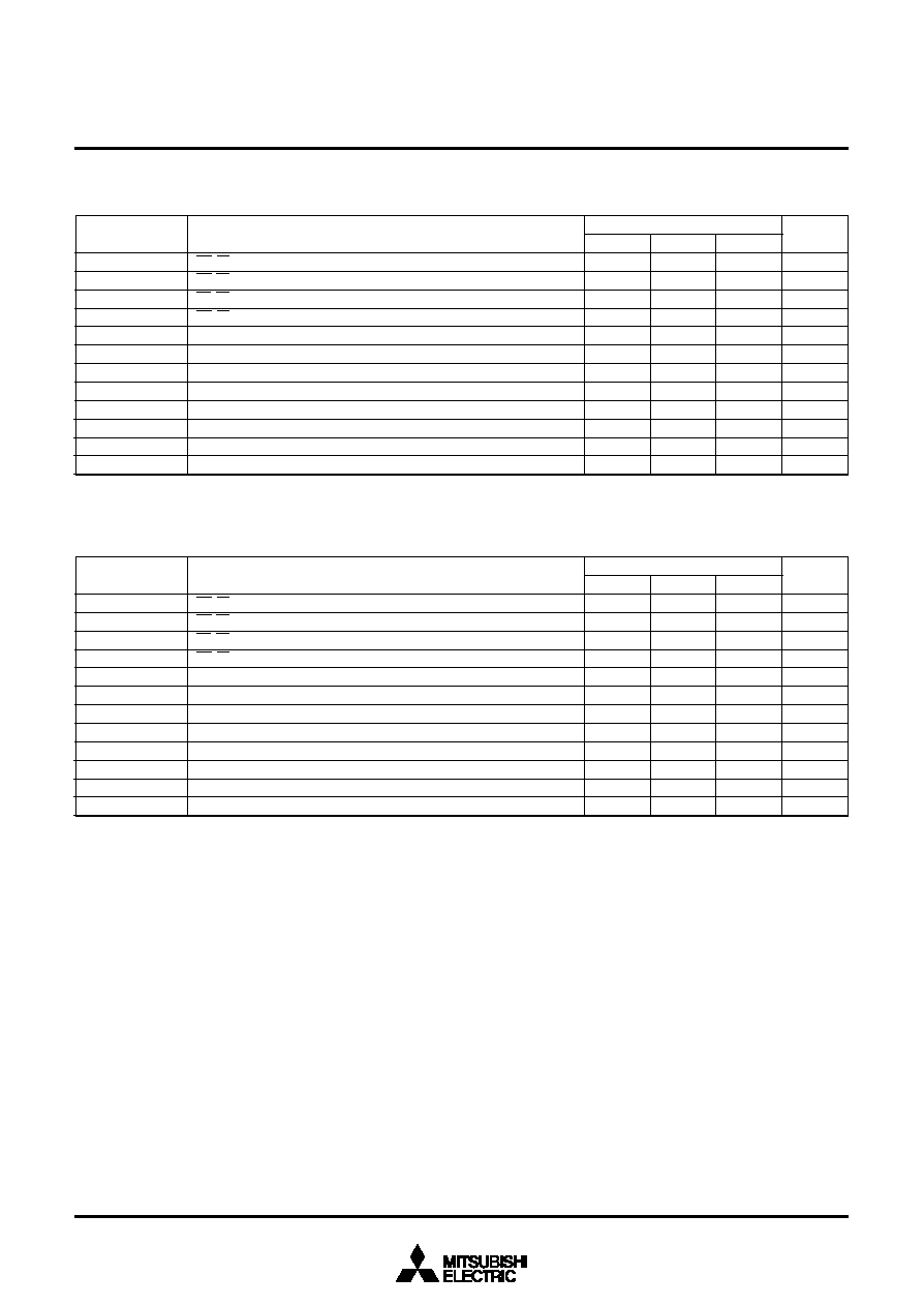
96
3886 Group
SINGLE-CHIP 8-BIT CMOS MICROCOMPUTER
MITSUBISHI MICROCOMPUTERS
Table 41 Timing requirements for system bus interface
(V
CC
= 2.7 to 4.0 V, V
SS
= 0 V, T
a
= ≠20 to 85 ∞C, unless otherwise noted)
Table 40 Timing requirements for system bus interface
(V
CC
= 4.0 to 5.5 V, V
SS
= 0 V, T
a
= ≠20 to 85 ∞C, unless otherwise noted)
S
0
, S
1
setup time
S
0
, S
1
setup time
S
0
, S
1
hold time
S
0
, S
1
hold time
A0 setup time
A0 setup time
A0 hold time
A0 hold time
t
su
(S-R)
t
su
(S-W)
t
h
(R-S)
t
h
(W-S)
t
su
(A-R)
t
su
(A-W)
t
h
(R-A)
t
h
(W-A)
Limits
ns
ns
ns
ns
ns
ns
ns
ns
ns
ns
ns
ns
Parameter
Min.
0
0
0
0
10
10
0
0
120
120
50
0
Typ.
Max.
Symbol
Unit
S
0
, S
1
setup time
S
0
, S
1
setup time
S
0
, S
1
hold time
S
0
, S
1
hold time
A0 setup time
A0 setup time
A0 hold time
A0 hold time
t
su
(S-R)
t
su
(S-W)
t
h
(R-S)
t
h
(W-S)
t
su
(A-R)
t
su
(A-W)
t
h
(R-A)
t
h
(W-A)
Limits
ns
ns
ns
ns
ns
ns
ns
ns
ns
ns
ns
ns
Parameter
Min.
0
0
0
0
30
30
0
0
250
250
130
0
Typ.
Max.
Symbol
Unit
Read pulse width
Write pulse width
Before write data input setup time
After write data input hold time
t
w
(R)
t
w
(W)
t
su
(D-W)
t
h
(W-D)
Read pulse width
Write pulse width
Before write data input setup time
After write data input hold time
t
w
(R)
t
w
(W)
t
su
(D-W)
t
h
(W-D)
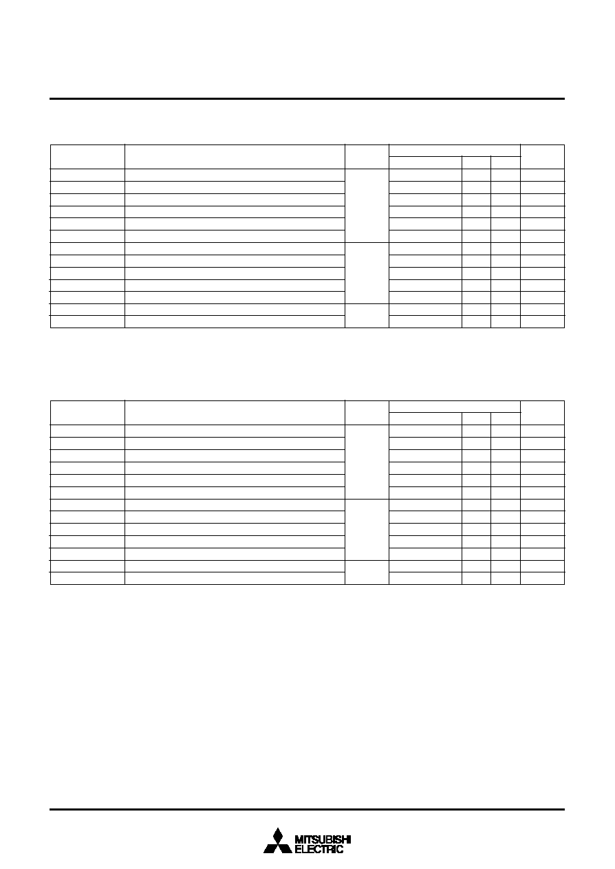
97
3886 Group
SINGLE-CHIP 8-BIT CMOS MICROCOMPUTER
MITSUBISHI MICROCOMPUTERS
Table 42 Switching characteristics 1
(V
CC
= 4.0 to 5.5 V, V
SS
= 0 V, T
a
= ≠20 to 85 ∞C, unless otherwise noted)
Serial I/O1 clock output "H" pulse width
Serial I/O1 clock output "L" pulse width
Serial I/O1 output delay time (Note 1)
Serial I/O1 output valid time (Note 1)
Serial I/O1 clock output rising time
Serial I/O1 clock output falling time
Serial I/O2 clock output "H" pulse width
Serial I/O2 clock output "L" pulse width
Serial I/O2 output delay time
Serial I/O2 output valid time
Serial I/O2 clock output falling time
CMOS output rising time (Note 2)
CMOS output falling time (Note 2)
t
WH
(S
CLK1
)
t
WL
(S
CLK1
)
t
d
(S
CLK1
-T
X
D)
t
V
(S
CLK1
-T
X
D)
t
r
(S
CLK1
)
t
f
(S
CLK1
)
t
WH
(S
CLK2
)
t
WL
(S
CLK2
)
t
d
(S
CLK2
-S
OUT2
)
t
V
(S
CLK2
-S
OUT2
)
t
f
(S
CLK2
)
t
r
(CMOS)
t
f
(CMOS)
Limits
ns
ns
ns
ns
ns
ns
ns
ns
ns
ns
ns
ns
ns
Parameter
Min.
t
C
(S
CLK1
)/2≠30
t
C
(S
CLK1
)/2≠30
≠30
t
C
(S
CLK2
)/2≠160
t
C
(S
CLK2
)/2≠160
0
Typ.
10
10
Max.
140
30
30
200
30
30
30
Symbol
Unit
Notes 1: When the P4
5
/T
X
D P-channel output disable bit of the UART control register (bit 4 of address 001B
16
) is "0".
2: The X
OUT
pin is excluded.
Test
conditions
Fig. 83
Fig. 84
Fig. 83
Table 43 Switching characteristics 2
(V
CC
= 2.7 to 4.0 V, V
SS
= 0 V, T
a
= ≠20 to 85 ∞C, unless otherwise noted)
Serial I/O1 clock output "H" pulse width
Serial I/O1 clock output "L" pulse width
Serial I/O1 output delay time (Note 1)
Serial I/O1 output valid time (Note 1)
Serial I/O1 clock output rising time
Serial I/O1 clock output falling time
Serial I/O2 clock output "H" pulse width
Serial I/O2 clock output "L" pulse width
Serial I/O2 output delay time
Serial I/O2 output valid time
Serial I/O2 clock output falling time
CMOS output rising time (Note 2)
CMOS output falling time (Note 2)
t
WH
(S
CLK1
)
t
WL
(S
CLK1
)
t
d
(S
CLK1
-T
X
D)
t
V
(S
CLK1
-T
X
D)
t
r
(S
CLK1
)
t
f
(S
CLK1
)
t
WH
(S
CLK2
)
t
WL
(S
CLK2
)
t
d
(S
CLK2
-S
OUT2
)
t
V
(S
CLK2
-S
OUT2
)
t
f
(S
CLK2
)
t
r
(CMOS)
t
f
(CMOS)
Limits
ns
ns
ns
ns
ns
ns
ns
ns
ns
ns
ns
ns
ns
Parameter
Min.
t
C
(S
CLK1
)/2≠50
t
C
(S
CLK1
)/2≠50
≠30
t
C
(S
CLK2
)/2≠240
t
C
(S
CLK2
)/2≠240
0
Typ.
20
20
Max.
350
50
50
400
50
50
50
Symbol
Unit
Notes 1: When the P4
5
/T
X
D P-channel output disable bit of the UART control register (bit 4 of address 001B
16
) is "0".
2: The X
OUT
pin is excluded.
Test
conditions
Fig. 83
Fig. 84
Fig. 83
98
3886 Group
SINGLE-CHIP 8-BIT CMOS MICROCOMPUTER
MITSUBISHI MICROCOMPUTERS
Table 44 Switching characteristics for system bus interface
(V
CC
= 4.0 to 5.5 V, V
SS
= 0 V, T
a
= ≠20 to 85 ∞C, unless otherwise noted)
After read data output enable time
After read data output disable time
After read OBF
00
, OBF
01
, OBF
10
output propagation time
t
a
(R-D)
t
v
(R-D)
t
PLH
(R-OBF)
Limits
ns
ns
ns
Parameter
Min.
Typ.
Max.
Symbol
Unit
0
80
30
150
Table 45 Switching characteristics for system bus interface
(V
CC
=2.7 to 4.0 V, V
SS
= 0 V, T
a
= ≠20 to 85 ∞C, unless otherwise noted)
After read data output enable time
After read data output disable time
After read OBF
00
, OBF
01
, OBF
10
output propagation time
t
a
(R-D)
t
v
(R-D)
t
PLH
(R-OBF)
Limits
ns
ns
ns
Parameter
Min.
Typ.
Max.
Symbol
Unit
0
130
85
300
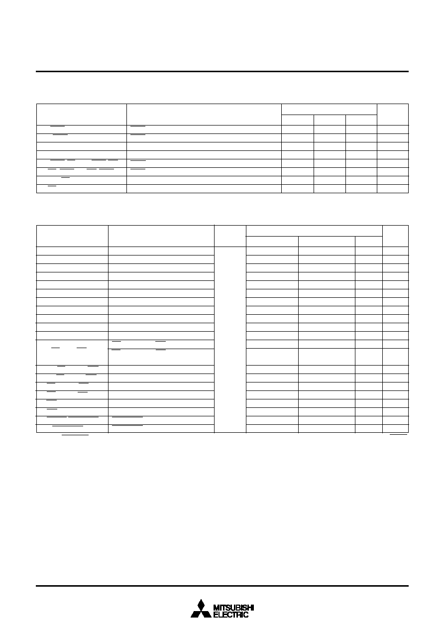
99
3886 Group
SINGLE-CHIP 8-BIT CMOS MICROCOMPUTER
MITSUBISHI MICROCOMPUTERS
Note: The RESET
OUT
output goes "H" in synchronized with the rise of the
clock that is anywhere between a few cycles and 10-several cycles after RESET
input goes "H".
Table 46 Timing requirements in memory expansion mode and microprocessor mode
(V
CC
= 4.0 to 5.5 V, V
SS
= 0 V, T
a
= ≠20 to 85 ∞C, in high-speed mode, unless otherwise noted)
ONW input setup time
ONW input hold time
Data bus setup time
Data bus hold time
ONW input setup time
ONW input hold time
Data bus setup time
Data bus hold time
t
su
(ONW-
)
t
h
(
-ONW)
t
su
(DB-
)
t
h
(
-DB)
t
su
(ONW-RD), t
su
(ONW-WR)
t
h
(RD-ONW), t
h
(WR-ONW)
t
su
(DB-RD)
t
h
(RD-DB)
Limits
ns
ns
ns
ns
ns
ns
ns
ns
Parameter
Min.
Typ.
Max.
Symbol
Unit
≠20
≠20
50
0
≠20
≠20
50
0
Table 47 Switching characteristics in memory expansion mode and microprocessor mode
(V
CC
= 4.0 to 5.5 V, V
SS
= 0 V, T
a
= ≠20 to 85 ∞C, in high-speed mode, unless otherwise noted)
clock cycle time
clock "H" pulse width
clock "L" pulse width
AD
15
≠AD
8
delay time
AD
7
≠AD
0
delay time
AD
15
≠AD
8
valid time
AD
7
≠AD
0
valid time
SYNC delay time
SYNC valid time
Data bus delay time
Data bus valid time
RD pulse width, WR pulse width
RD pulse width, WR pulse width
(When one-wait is valid)
AD
15
≠AD
8
delay time
AD
7
≠AD
0
delay time
AD
15
≠AD
8
valid time
AD
7
≠AD
0
valid time
Data bus delay time
Data bus valid time
RESET
OUT
output delay time
RESET
OUT
output valid time (Note)
t
C
(
)
t
WH
(
)
t
WL
(
)
t
d
(
-AH)
t
d
(
-AL)
t
V
(
-AH)
t
V
(
-AL)
t
d
(
-SYNC)
t
V
(
-SYNC)
t
d
(
-DB)
t
V
(
-DB)
t
WL
(RD), t
WL
(WR)
t
d
(AH-RD), t
d
(AH-WR)
t
d
(AL-RD), t
d
(AL-WR)
t
V
(RD-AH), t
V
(WR-AH)
t
V
(RD-AL), t
V
(WR-AL)
t
d
(WR-DB)
t
V
(WR-DB)
t
d
(RESET-RESET
OUT
)
t
V
(
-RESET
OUT
)
Limits
Parameter
Min.
Typ.
Max.
Symbol
Unit
Test
conditions
Fig. 83
ns
ns
ns
ns
ns
ns
ns
ns
ns
ns
ns
ns
ns
ns
ns
ns
ns
ns
ns
ns
ns
t
C
(X
IN
)≠10
t
C
(X
IN
)≠10
2
2
10
t
C
(X
IN
)≠10
3t
C
(X
IN
)≠10
t
C
(X
IN
)≠35
t
C
(X
IN
)≠40
2
2
10
0
35
40
30
30
200
100
2t
C
(X
IN
)
16
20
5
5
16
5
15
t
C
(X
IN
)≠16
t
C
(X
IN
)≠20
5
5
15
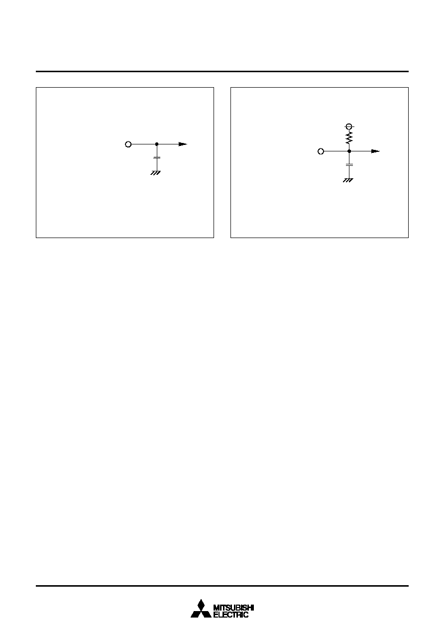
100
3886 Group
SINGLE-CHIP 8-BIT CMOS MICROCOMPUTER
MITSUBISHI MICROCOMPUTERS
Fig. 83 Circuit for measuring output switching characteristics (1)
Fig. 84 Circuit for measuring output switching characteristics (2)
M
e
a
s
u
r
e
m
e
n
t
o
u
t
p
u
t
p
i
n
1
0
0
p
F
C
M
O
S
o
u
t
p
u
t
N
-
c
h
a
n
n
e
l
o
p
e
n
≠
d
r
a
i
n
o
u
t
p
u
t
M
e
a
s
u
r
e
m
e
n
t
o
u
t
p
u
t
p
i
n
1
0
0
p
F
1
k

101
3886 Group
SINGLE-CHIP 8-BIT CMOS MICROCOMPUTER
MITSUBISHI MICROCOMPUTERS
Fig. 85 Timing diagram (1) (in single-chip mode)
0
.
2
V
C
C
t
W
L
(
I
N
T
)
0
.
8
V
C
C
t
W
H
(
I
N
T
)
0
.
2
V
C
C
0
.
2
V
C
C
0
.
8
V
C
C
0
.
8
V
C
C
0
.
2
V
C
C
t
W
L
(
X
I
N
)
0
.
8
V
C
C
t
W
H
(
X
I
N
)
t
C
(
X
I
N
)
X
I
N
0
.
2
V
C
C
0
.
8
V
C
C
t
W
(
R
E
S
E
T
)
R
E
S
E
T
t
f
t
r
0
.
2
V
C
C
t
W
L
(
C
N
T
R
)
0
.
8
V
C
C
t
W
H
(
C
N
T
R
)
t
C
(
C
N
T
R
)
t
d
(
S
C
L
K
1
-
T
X
D
)
,
t
d
(
S
C
L
K
2
-
S
O
U
T
2
)
t
v
(
S
C
L
K
1
-
T
X
D
)
,
t
v
(
S
C
L
K
2
-
S
O
U
T
2
)
t
C
(
S
C
L
K
1
)
,
t
C
(
S
C
L
K
2
)
t
W
L
(
S
C
L
K
1
)
,
t
W
L
(
S
C
L
K
2
)
t
W
H
(
S
C
L
K
1
)
,
t
W
H
(
S
C
L
K
2
)
t
h
(
S
C
L
K
1
-
R
x
D
)
,
t
h
(
S
C
L
K
2
-
S
I
N
2
)
t
s
u
(
R
x
D
-
S
C
L
K
1
)
,
t
s
u
(
S
I
N
2
-
S
C
L
K
2
)
T
X
D
S
O
U
T
2
R
X
D
S
I
N
2
S
C
L
K
1
S
C
L
K
2
I
N
T
0
,
I
N
T
1
I
N
T
2
0
,
I
N
T
3
0
,
I
N
T
4
0
I
N
T
2
1
,
I
N
T
3
1
,
I
N
T
4
1
C
N
T
R
0
,
C
N
T
R
1
T
i
m
i
n
g
d
i
a
g
r
a
m
i
n
s
i
n
g
l
e
-
c
h
i
p
m
o
d
e
0
.
2
V
C
C
t
W
L
(
X
C
I
N
)
0
.
8
V
C
C
t
W
H
(
X
C
I
N
)
t
C
(
X
C
I
N
)
X
C
I
N
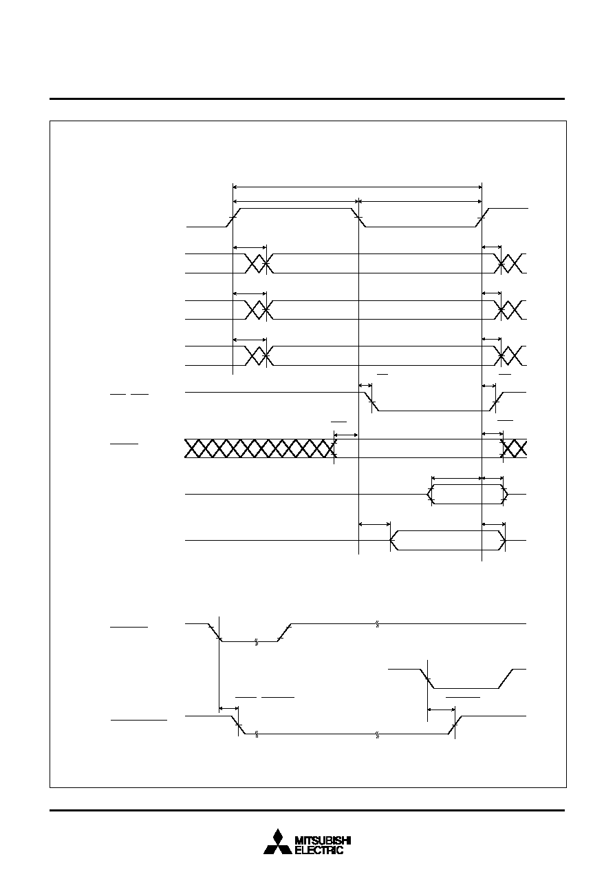
102
3886 Group
SINGLE-CHIP 8-BIT CMOS MICROCOMPUTER
MITSUBISHI MICROCOMPUTERS
Fig. 86 Timing diagram (2) (in memory expansion mode and microprocessor mode)
t
W
L
(
)
0
.
5
V
C
C
t
W
H
(
)
t
C
(
)
t
d
(
-
A
H
)
t
d
(
-
A
L
)
t
d
(
-
S
Y
N
C
)
t
v
(
-
A
H
)
t
v
(
-
A
L
)
t
v
(
-
S
Y
N
C
)
t
d
(
-
W
R
)
t
v
(
-
W
R
)
0
.
5
V
C
C
0
.
5
V
C
C
0
.
5
V
C
C
0
.
5
V
C
C
t
S
U
(
O
N
W
-
)
t
h
(
-
O
N
W
)
0
.
8
V
C
C
0
.
2
V
C
C
0
.
8
V
C
C
0
.
2
V
C
C
t
S
U
(
D
B
-
)
t
h
(
-
D
B
)
0
.
5
V
C
C
t
d
(
-
D
B
)
t
v
(
-
D
B
)
0
.
2
V
C
C
0
.
8
V
C
C
0
.
5
V
C
C
t
d
(
R
E
S
E
T
-
R
E
S
E
T
O
U
T
)
0
.
5
V
C
C
A
D
1
5
≠
A
D
8
A
D
7
≠
A
D
0
S
Y
N
C
R
D
,
W
R
O
N
W
D
B
0
≠
D
B
7
D
B
0
≠
D
B
7
R
E
S
E
T
R
E
S
E
T
O
U
T
t
v
(
-
R
E
S
E
T
O
U
T
)
(
A
t
C
P
U
r
e
a
d
i
n
g
)
(
A
t
C
P
U
w
r
i
t
i
n
g
)
T
i
m
i
n
g
d
i
a
g
r
a
m
i
n
m
e
m
o
r
y
e
x
p
a
n
s
i
o
n
m
o
d
e
a
n
d
m
i
c
r
o
p
r
o
c
e
s
s
o
r
m
o
d
e
(
1
)
T
i
m
i
n
g
d
i
a
g
r
a
m
i
n
m
i
c
r
o
p
r
o
c
e
s
s
o
r
m
o
d
e
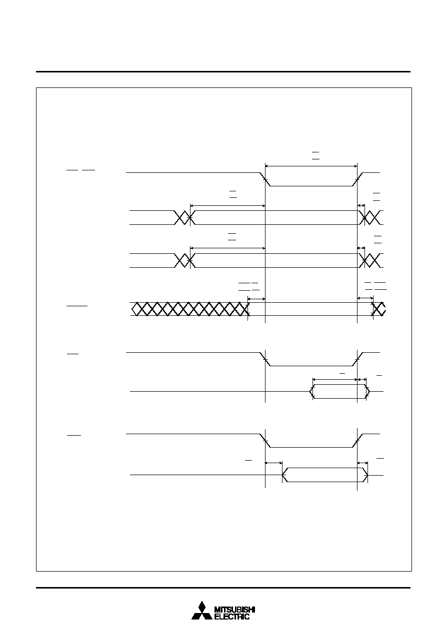
103
3886 Group
SINGLE-CHIP 8-BIT CMOS MICROCOMPUTER
MITSUBISHI MICROCOMPUTERS
Fig. 87 Timing diagram (3) (in memory expansion mode and microprocessor mode)
0
.
5
V
C
C
R
D
,
W
R
0
.
5
V
C
C
A
D
1
5
≠
A
D
8
t
d
(
A
H
-
W
R
)
t
v
(
W
R
-
A
H
)
0
.
5
V
C
C
A
D
7
≠
A
D
0
t
d
(
A
L
-
W
R
)
t
v
(
W
R
-
A
L
)
0
.
8
V
C
C
0
.
2
V
C
C
D
B
0
≠
D
B
7
0
.
5
V
C
C
R
D
t
S
U
(
D
B
-
R
D
)
t
h
(
R
D
-
D
B
)
0
.
5
V
C
C
D
B
0
≠
D
B
7
0
.
5
V
C
C
W
R
t
d
(
W
R
-
D
B
)
t
v
(
W
R
-
D
B
)
t
h
(
W
R
-
O
N
W
)
0
.
8
V
C
C
0
.
2
V
C
C
O
N
W
t
s
u
(
O
N
W
-
W
R
)
t
v
(
R
D
-
A
H
)
t
d
(
A
H
-
R
D
)
t
d
(
A
L
-
R
D
)
t
v
(
R
D
-
A
L
)
t
h
(
R
D
-
O
N
W
)
t
s
u
(
O
N
W
-
R
D
)
t
W
L
(
R
D
)
t
W
L
(
W
R
)
(
A
t
C
P
U
r
e
a
d
i
n
g
)
(
A
t
C
P
U
w
r
i
t
i
n
g
)
T
i
m
i
n
g
d
i
a
g
r
a
m
i
n
m
e
m
o
r
y
e
x
p
a
n
s
i
o
n
m
o
d
e
a
n
d
m
i
c
r
o
p
r
o
c
e
s
s
o
r
m
o
d
e
(
2
)
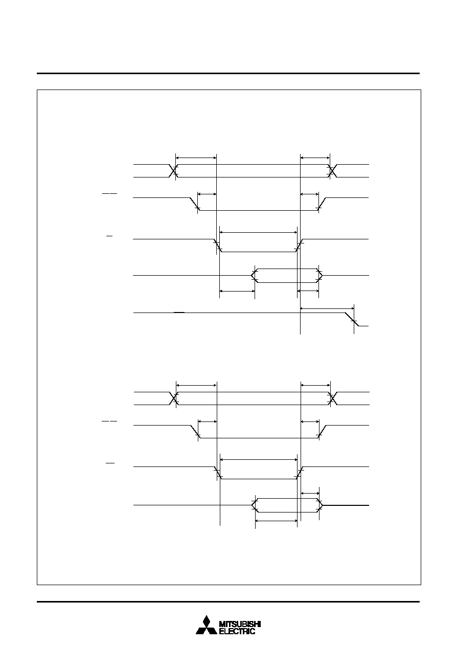
104
3886 Group
SINGLE-CHIP 8-BIT CMOS MICROCOMPUTER
MITSUBISHI MICROCOMPUTERS
Fig. 88 Timing diagram (4) (system bus interface)
0
.
4
5
(
0
.
2
V
C
C
)
2
.
4
(
0
.
8
V
C
C
)
0
.
4
5
(
0
.
2
V
C
C
)
2
.
4
(
0
.
8
V
C
C
)
0
.
4
5
(
0
.
2
V
C
C
)
0
.
4
5
(
0
.
2
V
C
C
)
t
s
u
(
A
-
R
)
t
h
(
R
-
A
)
t
s
u
(
S
-
R
)
t
h
(
R
-
S
)
0
.
4
5
(
0
.
2
V
C
C
)
0
.
4
5
(
0
.
2
V
C
C
)
t
w
(
R
)
2
.
4
(
0
.
8
V
C
C
)
2
.
4
(
0
.
8
V
C
C
)
2
.
0
(
0
.
8
V
C
C
)
2
.
0
(
0
.
8
V
C
C
)
0
.
8
(
0
.
2
V
C
C
)
0
.
8
(
0
.
2
V
C
C
)
t
a
(
R
-
D
)
t
v
(
R
-
D
)
0
.
8
(
0
.
2
V
C
C
)
t
P
L
H
(
R
-
O
B
F
)
A
0
R
O
B
F
0
0
,
O
B
F
0
1
,
O
B
F
1
0
0
.
4
5
(
0
.
2
V
C
C
)
2
.
4
(
0
.
8
V
C
C
)
0
.
4
5
(
0
.
2
V
C
C
)
2
.
4
(
0
.
8
V
C
C
)
0
.
4
5
(
0
.
2
V
C
C
)
0
.
4
5
(
0
.
2
V
C
C
)
t
s
u
(
A
-
W
)
t
h
(
W
-
A
)
t
s
u
(
S
-
W
)
t
h
(
W
-
S
)
0
.
4
5
(
0
.
2
V
C
C
)
0
.
4
5
(
0
.
2
V
C
C
)
t
w
(
W
)
2
.
4
(
0
.
8
V
C
C
)
2
.
4
(
0
.
8
V
C
C
)
t
s
u
(
D
-
W
)
t
h
(
W
-
D
)
A
0
W
0
.
4
5
(
0
.
2
V
C
C
)
2
.
4
(
0
.
8
V
C
C
)
0
.
4
5
(
0
.
2
V
C
C
)
2
.
4
(
0
.
8
V
C
C
)
S
0
,
S
1
R
e
a
d
o
p
e
r
a
t
i
o
n
W
r
i
t
e
o
p
e
r
a
t
i
o
n
O
u
t
s
i
d
e
o
f
p
a
r
e
n
t
h
e
s
i
s
:
T
T
L
I
/
O
I
n
s
i
d
e
o
f
p
a
r
e
n
t
h
e
s
i
s
:
C
M
O
S
I
/
O
D
Q
0
≠
D
Q
7
D
Q
0
≠
D
Q
7
S
0
,
S
1
S
y
s
t
e
m
b
u
s
i
n
t
e
r
f
a
c
e
t
i
m
i
n
g
d
i
a
g
r
a
m
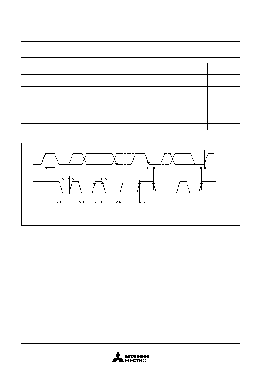
105
3886 Group
SINGLE-CHIP 8-BIT CMOS MICROCOMPUTER
MITSUBISHI MICROCOMPUTERS
Symbol
Parameter
Unit
Table 48 Multi-master I
2
C-BUS bus line characteristics
Bus free time
Hold time for START condition
Hold time for S
CL
clock = "0"
Rising time of both S
CL
and S
DA
signals
Data hold time
Hold time for S
CL
clock = "1"
Falling time of both S
CL
and S
DA
signals
Data setup time
Setup time for repeated START condition
Setup time for STOP condition
t
BUF
t
HD;STA
t
LOW
t
R
t
HD;DAT
t
HIGH
t
F
t
SU;DAT
t
SU;STA
t
SU;STO
Min.
Max.
Min.
Max.
µ
s
µ
s
µ
s
ns
µ
s
µ
s
ns
ns
µ
s
µ
s
Standard clock mode
High-speed clock mode
Note: C
b
= total capacitance of 1 bus line
Fig. 89 Timing diagram of multi-master I
2
C-BUS
4.7
4.0
4.7
0
4.0
250
4.7
4.0
1000
300
1.3
0.6
1.3
20+0.1C
b
0
0.6
20+0.1C
b
100
0.6
0.6
300
0.9
300
t
B
U
F
t
H
D
:
S
T
A
t
H
D
:
D
A
T
t
L
O
W
t
R
t
F
t
H
I
G
H
t
s
u
:
D
A
T
t
s
u
:
S
T
A
t
H
D
:
S
T
A
t
s
u
:
S
T
O
S
C
L
P
S
S
r
P
S
D
A
S :
S
T
A
R
T
c
o
n
d
i
t
i
o
n
S
r:
R
E
S
T
A
R
T
c
o
n
d
i
t
i
o
n
P :
S
T
O
P
c
o
n
d
i
t
i
o
n
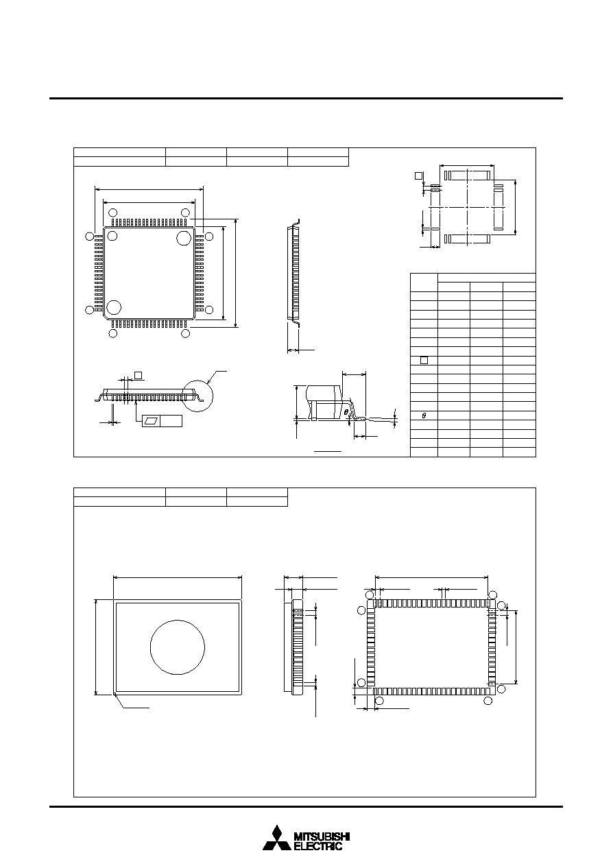
106
3886 Group
SINGLE-CHIP 8-BIT CMOS MICROCOMPUTER
MITSUBISHI MICROCOMPUTERS
PACKAGE OUTLINE
LQFP80-P-1212-0.5
Weight(g)
≠
JEDEC Code
EIAJ Package Code
Lead Material
Cu Alloy
80P6Q-A
Plastic 80pin 12
!
12mm body LQFP
≠
0.1
≠
≠
≠
0.2
≠
≠
≠
≠
≠
≠
≠
≠
≠
Symbol
Min
Nom
Max
A
A
2
b
c
D
E
H
E
L
L
1
y
b
2
Dimension in Millimeters
H
D
A
1
0.225
≠
≠
I
2
1.0
≠
≠
M
D
12.4
≠
≠
M
E
12.4
10
∞
0
∞
0.1
1.0
0.7
0.5
0.3
14.2
14.0
13.8
14.2
14.0
13.8
0.5
12.1
12.0
11.9
12.1
12.0
11.9
0.175
0.125
0.105
0.28
0.18
0.13
1.4
0
1.7
e
A
L
1
c
L
A
1
A
2
F
b
e
H
D
E
H
E
D
1
20
21
40
41
60
61
80
M
E
b
2
l
2
M
D
e
Recommended Mount Pad
Detail F
y
Weight(g)
JEDEC Code
EIAJ Package Code
80D0
Glass seal 80pin QFN
≠
≠
25
40
80
65
41
64
24
1
1.2TYP
0.6TYP
0.8TYP
INDEX
1.78TYP
3.32MAX
0.8TYP
1.2TYP
0.8TYP
0.5TYP
12.0
±
0.15
15.6
±
0.2
21.0
±
0.2
18.4
±
0.15

107
3886 Group
SINGLE-CHIP 8-BIT CMOS MICROCOMPUTER
MITSUBISHI MICROCOMPUTERS
QFP80-P-1414-0.65
1.11
Weight(g)
JEDEC Code
EIAJ Package Code
Lead Material
Alloy 42
80P6S-A
Plastic 80pin 14
!
14mm body QFP
≠
0.1
≠
≠
≠
0.2
≠
≠
≠
≠
≠
≠
≠
≠
≠
Symbol
Min
Nom
Max
A
A
2
b
c
D
E
H
E
L
L
1
y
b
2
Dimension in Millimeters
H
D
A
1
0.35
≠
≠
I
2
1.3
≠
≠
M
D
14.6
≠
≠
M
E
14.6
10
∞
0
∞
0.1
1.4
0.8
0.6
0.4
17.1
16.8
16.5
17.1
16.8
16.5
0.65
14.2
14.0
13.8
14.2
14.0
13.8
0.2
0.15
0.13
0.4
0.3
0.25
2.8
0
3.05
e
e
e
E
c
H
E
1
80
61
40
60
41
21
20
H
D
D
M
D
M
E
A
F
A
1
A
2
L
1
L
y
b
2
I
2
Recommended Mount Pad
Detail F
x
≠
≠
0.13
b
x
M

Rev.
Rev.
No.
date
1.0
First Edition
980216
2.0
The contents of flash memory version were added.
980716
2.1
All pages; "PRELIMINARY Notice: This is..." eliminated.
000114
Page 1; The second "In high-speed mode" of "Power dissipation" eliminated.
Page 1; "Memory expansion" is revised.
Page 1; Explanation of "<Flash memory mode>" is revised.
Page 1; Notes 2 is changed.
Page 1; Some words of "APPLICATION" are added.
Page 2; Figure 1 and Figure 2 are partly revised.
Page 3; Figure 3 is added.
Page 7; Figure 5 is partly revised.
Page 8; Figure 6 is partly revised.
Page 8; Some products are added into Table 3.
Page 9; Note into Figure 7 is revised.
Page 10; Note into Figure 8 is revised.
Page 11; Note into Figure 9 is added.
Page 41; Explanation of "I
2
C Data Shift Register" is partly revised.
Page 42; Explanation of "I
2
C Clock Control Regsiter" is partly revised.
Page 42; Note 1 into Table 10 is partly revised.
Page 50; (6) and (7) of "Precaution when using multi-master I
2
C BUS interface" are added.
Page 51; Figure 48 is partly revised.
Page 56; Explanation of "RESET CIRCUIT" is partly revised.
Page 56; Note into Figure 55 is revised.
Page 60; Figure 61 is partly revised.
Page 61; Explanation of "PROCESSOR MODE" is partly revised.
Page 61; Explanation into Figure 62 is eliminated partly.
Page 61; Note into Figure 63 is revised.
Page 66; Figure 66 is partly revised.
REVISION DESCRIPTION LIST
3886 GROUP DATA SHEET
(1/2)
Revision Description
Rev.
Rev.
No.
date
2.1
Page 73; Minimum limits of V
PP
H into Table 22 is revised.
000114
Page 74; Figure 72 is partly revised.
Page 81; Explanation of "Flash memory mode 3 (CPU reprogramming mode)" is added.
Page 81; Note into Figure 79 is eliminated partly.
Page 82; "CPU reprogramming mode operation procedure" is eliminated partly.
Page 82; Figure 81 is partly revised.
Page 86; Explanation of "Handling of Power Source Pins" is added.
Page 86; Explanation of "Erasing of Flash memory version" is added.
Page 87; Parameter into Table 28 is partly revised.
Page 88; Parameter into Table 29 is partly revised.
∑Mask ROM confirmation forms are eliminated.
V
Refer to the "Mitsubishi MCU Technical Information" Homepage (http://www.infomicom.
mesc.co.jp/indexe/htm). [38000 Series
Mask ROM Confirmation Forms]
∑ROM programming confirmation form is eliminated.
V
Refer to the "Mitsubishi MCU Technical Information" Homepage (http://www.infomicom.
mesc.co.jp/indexe/htm). [38000 Series
Mask ROM Confirmation Forms]
∑Mark specification form is eliminated.
V
Refer to the "Mitsubishi MCU Technical Information" Homepage (http://www.infomicom.
mesc.co.jp/indexe/htm). [38000 Series
Mask ROM Confirmation Forms
ROM
Ordering Method
Mark Specification Forms]
Page 107; Package outline for 80P6S-A is added.
REVISION DESCRIPTION LIST
3886 GROUP DATA SHEET
(2/2)
Revision Description

© 2000 MITSUBISHI ELECTRIC CORP.
H-LF492-A KI-0001 Printed in Japan (ROD)
II
New publication, effective Jan. 2000.
Specifications subject to change without notice.
Notes regarding these materials
∑
These materials are intended as a reference to assist our customers in the selection of the Mitsubishi semiconductor product best suited to the customer's application; they do not convey any license under any intellectual property
rights, or any other rights, belonging to Mitsubishi Electric Corporation or a third party.
∑
Mitsubishi Electric Corporation assumes no responsibility for any damage, or infringement of any third-party's rights, originating in the use of any product data, diagrams, charts, programs, algorithms, or circuit application examples
contained in these materials.
∑
All information contained in these materials, including product data, diagrams, charts, programs and algorithms represents information on products at the time of publication of these materials, and are subject to change by
Mitsubishi Electric Corporation without notice due to product improvements or other reasons. It is therefore recommended that customers contact Mitsubishi Electric Corporation or an authorized Mitsubishi Semiconductor product
distributor for the latest product information before purchasing a product listed herein.
The information described here may contain technical inaccuracies or typographical errors. Mitsubishi Electric Corporation assumes no responsibility for any damage, liability, or other loss rising from these inaccuracies or errors.
Please also pay attention to information published by Mitsubishi Electric Corporation by various means, including the Mitsubishi Semiconductor home page (http://www.mitsubishichips.com).
∑
When using any or all of the information contained in these materials, including product data, diagrams, charts, programs, and algorithms, please be sure to evaluate all information as a total system before making a final decision
on the applicability of the information and products. Mitsubishi Electric Corporation assumes no responsibility for any damage, liability or other loss resulting from the information contained herein.
∑
Mitsubishi Electric Corporation semiconductors are not designed or manufactured for use in a device or system that is used under circumstances in which human life is potentially at stake. Please contact Mitsubishi Electric
Corporation or an authorized Mitsubishi Semiconductor product distributor when considering the use of a product contained herein for any specific purposes, such as apparatus or systems for transportation, vehicular, medical,
aerospace, nuclear, or undersea repeater use.
∑
The prior written approval of Mitsubishi Electric Corporation is necessary to reprint or reproduce in whole or in part these materials.
∑
If these products or technologies are subject to the Japanese export control restrictions, they must be exported under a license from the Japanese government and cannot be imported into a country other than the approved
destination.
Any diversion or reexport contrary to the export control laws and regulations of Japan and/or the country of destination is prohibited.
∑
Please contact Mitsubishi Electric Corporation or an authorized Mitsubishi Semiconductor product distributor for further details on these materials or the products contained therein.
Keep safety first in your circuit designs!
∑
Mitsubishi Electric Corporation puts the maximum effort into making semiconductor products better and more reliable, but there is always the possibility that trouble may occur with them. Trouble with semiconductors may lead to
personal injury, fire or property damage. Remember to give due consideration to safety when making your circuit designs, with appropriate measures such as (i) placement of substitutive, auxiliary circuits, (ii) use of non-flammable
material or (iii) prevention against any malfunction or mishap.
HEAD OFFICE: 2-2-3, MARUNOUCHI, CHIYODA-KU, TOKYO 100-8310, JAPAN