1
SINGLE-CHIP 8-BIT CMOS MICROCOMPUTER
MITSUBISHI MICROCOMPUTERS
38K0 Group
DESCRIPTION
The 38K0 group is the 8-bit microcomputer based on the 740 fam-
ily core technology.
The 38K0 group has the USB function, an 8-bit bus interface, a
Serial I/O, three 8-bit timers, and an 8-channel 10-bit A-D con-
verter, which are available for the PC peripheral I/O device.
The various microcomputers in the 38K0 group include variations
of internal memory size and packaging. For details, refer to the
section on part numbering.
FEATURES
�
Basic machine-language instructions ....................................... 71
�
The minimum instruction execution time .......................... 0.25 �s
(at 8 MHz system clock
)
System clock
: Reference frequency to internal circuit except
USB function
�
Memory size
ROM ................................................................ 16 K to 32 K bytes
RAM ............................................................... 1024 to 2048 bytes
�
Programmable input/output ports ............................................. 48
�
Software pull-up resistors
�
Interrupts .................................................. 15 sources, 15 vectors
�
USB function (USB version 1.1 specification) ........... 4 endpoints
�
External bus interface ....................................... 8-bit
1 channel
�
Timers ............................................................................. 8-bit
3
�
Watchdog timer ............................................................. 16-bit
1
�
Serial I/O ...................... 8-bit
1 (UART or Clock-synchronized)
�
A-D converter ................................................ 10-bit
8 channels
(8-bit reading available)
�
LED direct drive port ................................................................... 4
�
Clock generating circuit
(connect to external ceramic resonator or quartz-crystal oscillator)
�
Power source voltage
System clock/Internal clock division mode
At 12 MHz/Through mode (
= 12 MHz) ......................................
......................................................... 4.50 to 5.25 V (under planning)
At 12 MHz/2-divide mode(
= 6 MHz) ..........................................
............................................. 4.00 to 5.25 V (under development)
At 8 MHz/Through mode (
= 8 MHz) ................... 4.00 to 5.25 V
At 6 MHz/Through mode (
= 6 MHz) ................... 4.00 to 5.25 V
At 6 MHz/Through mode (
= 6 MHz) ..........................................
............................................. 3.00 to 4.00 V (under development)
Remarks: The mode under development will be available from
Aug./2002.
�
Power dissipation
At 5 V power source voltage .................................. 125 mW (typ.)
(at 8 MHz system clock, in through mode)
At 3.3 V power source voltage ................................ 45 mW (typ.)
(at 6 MHz system clock, in through mode)
�
Operating temperature range .................................... �20 to 85�C
�
Packages
FP ........................................ 64P6U-A (64-pin 14
14 mm LQFP)
HP ........................................ 64P6Q-A (64-pin 10
10 mm LQFP)
s
Notes
1. The specifications of this product are subject to change be-
cause it is under development. Inquire the use of Mitsubishi
Electric Corporation.
2. The flash memory version cannot be used for application em-
bedded in the MCU card.
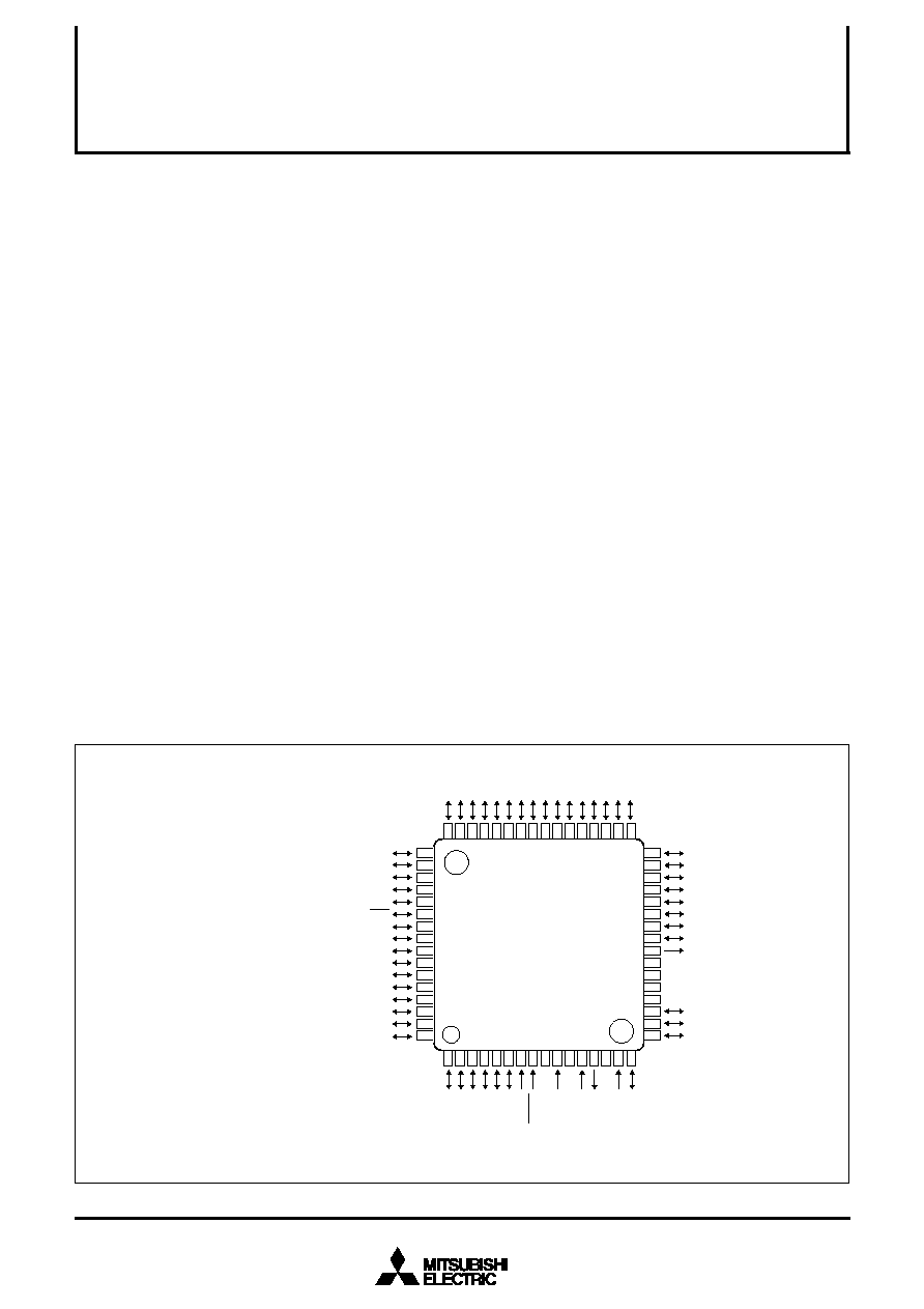
Package type : 64P6U-A/64P6Q-A
Fig. 1 Pin configuration of 38K0 group
PIN CONFIGURATION (TOP VIEW)
32
31
30
29
28
26
25
24
23
22
21
20
19
18
17
49
50
51
52
53
54
55
56
57
58
59
60
61
62
63
27
64
4
8
4
7
4
6
4
5
4
3
4
2
4
1
4
0
3
9
3
8
3
7
3
6
3
5
3
4
3
3
4
4
1
2
3
4
5
6
7
8
9
1
0
1
1
1
2
1
3
1
4
1
5
1
6
T
r
O
N
P
2
3
P
2
2
P
2
1
P
2
0
D
0
-
D
0
+
USBV
REF
DV
CC
P
V
C
C
P
0
3
P
0
2
P
0
1
P
0
0
P
5
7
P
5
6
P
5
5
P
5
4
P
5
3
P
5
2
/
I
N
T
1
P
5
1
/
C
N
T
R
P
5
0
/
I
N
T
0
P
V
S
S
P1
0
/DQ
0
/AN
0
P
0
6
P
0
7
P
4
0
/
E
X
D
R
E
Q
/
R
X
D
P1
1
/DQ
1
/AN
1
P
1
2
/
D
Q
2
/
A
N
2
P
1
3
/
D
Q
3
/
A
N
3
P
1
4
/
D
Q
4
/
A
N
4
P
1
5
/
D
Q
5
/
A
N
5
P
1
6
/
D
Q
6
/
A
N
6
P
1
7
/
D
Q
7
/
A
N
7
P
6
0
(
L
E
D
0
)
P
6
1
(
L
E
D
1
)
P
6
2
(
L
E
D
2
)
P
6
3
(
L
E
D
3
)
P
4
1
/
E
X
D
A
C
K
/
T
X
D
P
4
2
/
E
X
T
C
/
S
C
L
K
P4
3
/E
X
A1/S
RDY
P
3
0
P
3
1
P
3
2
P
3
3
/
E
X
I
N
T
P
3
4
/
E
X
C
S
P3
5
/E
X
WR
P3
6
/E
X
RD
P
3
7
/
E
X
A
0
M
3
8
K
0
7
M
4
-
X
X
X
F
P
/
H
P
M
3
8
K
0
9
F
8
F
P
/
H
P
P
2
4
P
0
4
P
2
7
P
2
6
C
N
V
S
S
V
C
C
E
V
R
E
F
V
S
S
X
O
U
T
V
C
C
C
N
V
S
S
2
X
I
N
R
E
S
E
T
P
2
5
P
0
5
3
SINGLE-CHIP 8-BIT CMOS MICROCOMPUTER
MITSUBISHI MICROCOMPUTERS
38K0 Group
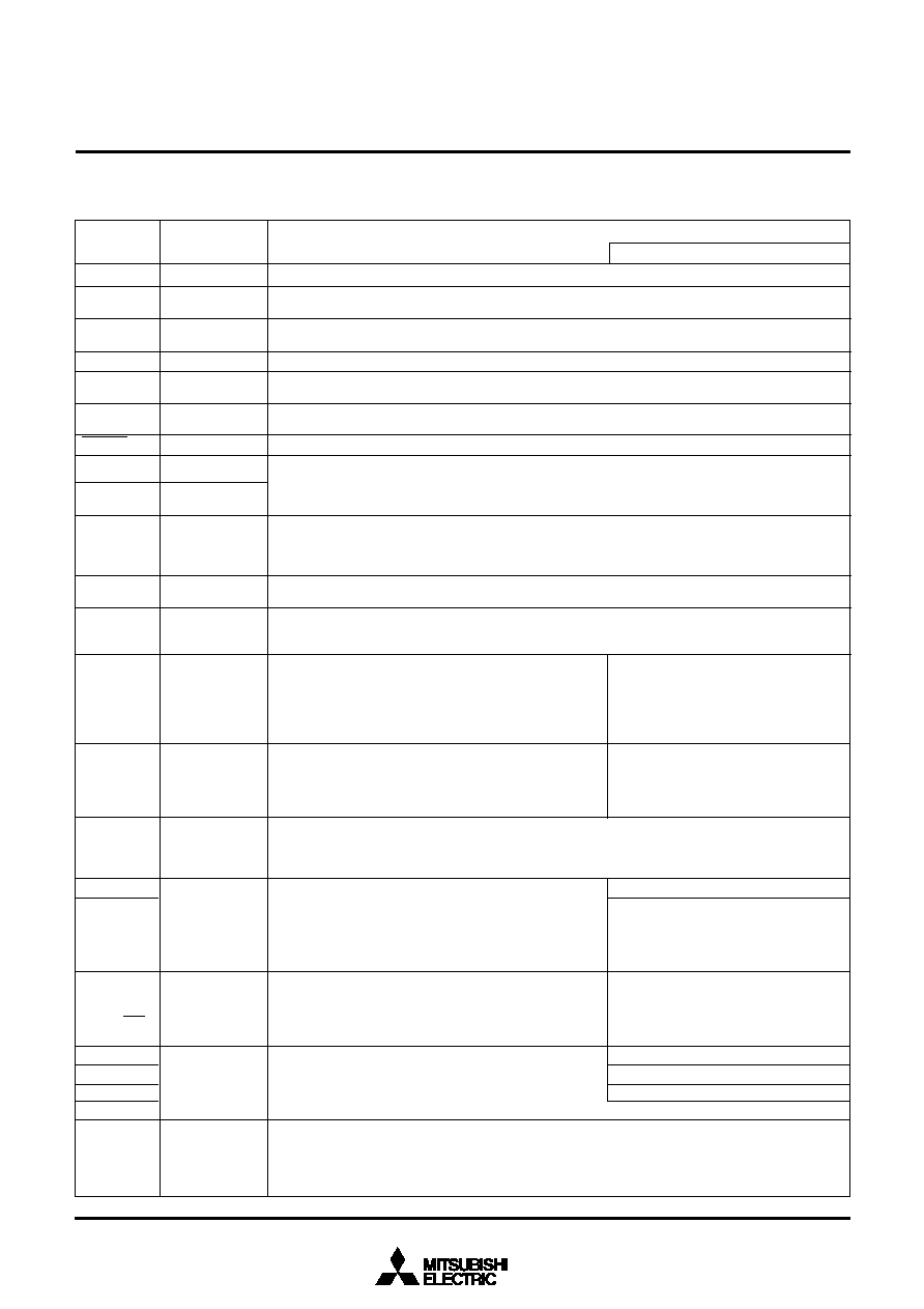
PIN DESCRIPTION
Table 1. Pin description
Function
� Apply voltage of 3.0 V � 5.25 V to V
CC
, and 0 V to V
SS
.
� Power source pin for ports P1, P3, P4 and analog circuit. Connect this pin to V
CC
.
� This pin controls the operation mode of the chip. Connect this pin to V
SS
. In the flash memory
mode, this pin becoems V
PP
power source input pin.
� This pin controls the operation mode of the chip. Connect this pin to V
SS
.
� Reference voltage input pin for A-D converter.
� Power source pin for analog circuit.
� Connect the DV
CC
and PV
CC
pins to V
CC
, and the PV
SS
pin to V
SS
.
� Reset input pin for active "L"
� Input and output pins for the main clock generating circuit.
� Connect a ceramic resonator or a quartz-crystal oscillator between the X
IN
and X
OUT
pins to set
the oscillation frequency.
�If an external clock is used, connect the clock source to the X
IN
pin and leave the X
OUT
pin open.
� Power source pin for USB port circuit.
In Vcc = 4.00 to 5.25 V use the built-in USB reference voltage circuit. In Vcc = 3.00 to 4.00 V apply
3.3 V power supply from the external because use of the built-in USB reference voltage circuit is
prohibited in this voltage range. In Vcc = 3.00 to 3.60 V connect this pin to V
CC
.
� Output pin to pull-up D0+ by 1.5 k
external resistor.
� USB upstream I/O port
� USB input level
� USB output level output structure
� 8-bit I/O port
� I/O direction register allows each pin to be individually
programmed as either input or output.
� CMOS compatible input level
� CMOS 3-state output structure
� Pull-up control is enabled.
� 8-bit I/O port
� I/O direction register allows each pin to be individually
programmed as either input or output.
� CMOS compatible input level
� CMOS 3-state output structure
� 8-bit I/O port
� I/O direction register allows each pin to be individually programmed as either input or output.
� CMOS compatible input level
� CMOS 3-state output structure
� 8-bit I/O port
� I/O direction register allows each pin to be individually
programmed as either input or output.
� CMOS compatible input level
� CMOS 3-state output structure
� 4-bit I/O port
� I/O direction register allows each pin to be individually
programmed as either input or output.
� CMOS compatible input level
� CMOS 3-state output structure
� 8-bit I/O port
� I/O direction register allows each pin to be individually
programmed as either input or output.
� CMOS compatible input level
� CMOS 3-state output structure
� 4-bit I/O port
� I/O direction register allows each pin to be individually programmed as either input or output.
� CMOS compatible input level
� CMOS 3-state output structure
� Output large current for LED drive is enabled.
� Key input pins (key-on wake up interrupt)
� A-D converter input pins
� External bus interface function pins
� External bus interface function pins
� Serial I/O function pins
� External bus interface function pins
� Interrupt input pin
� Timer X funciton pin
� Interrupt input pin
Pin
V
CC
, V
SS
V
CC
E
CNV
SS
CNV
SS
2
V
REF
DV
CC
PV
CC
, PV
SS
RESET
X
IN
X
OUT
USBV
REF
TrON
D0+, D0-
P0
0
�P0
7
P1
0
/DQ
0
/AN
0
�
P1
7
/DQ
7
/AN
7
P2
0
�P2
7
P3
0
�P3
2
P3
3
/ExINT
P3
4
/ExCS
P3
5
/ExWR
P3
6
/ExRD
P3
7
/ExA0
P4
0
/ExDREQ/RxD
P4
1
/ExDACK/TxD
P4
2
/ExTC/S
CLK
P4
3
/ExA1/S
RDY
P5
0
/INT
0
P5
1
/CNTR
0
P5
2
/INT
1
P5
3
�P5
7
P6
0
�P6
3
Name
Power source
Analog power
source
CNV
SS
CNV
SS
2
Analog reference
voltage input
Analog power
source
Reset input
Clock input
Clock output
USB reference
power source
USB reference
voltage output
USB upstream
I/O
I/O port P0
I/O port P1
I/O port P2
I/O port P3
I/O port P4
I/O port P5
I/O port P6
Function except a port function

5
SINGLE-CHIP 8-BIT CMOS MICROCOMPUTER
MITSUBISHI MICROCOMPUTERS
38K0 Group
GROUP EXPANSION
Mitsubishi plans to expand the 38K0 group as follows.
Memory Type
Support for mask ROM and flash memory versions.
Memory Size
Flash memory size .......................................................... 32 Kbytes
Mask ROM size ............................................................... 16 Kbytes
RAM size .......................................................... 1024 to 2048 bytes
Packages
64P6U-A .................................. 0.8 mm-pitch plastic molded LQFP
64P6Q-A .................................. 0.5 mm-pitch plastic molded LQFP
100D0M ........................... 0.65 mm-pitch metal seal PIGGY BACK
Memory Expansion Plan
Fig. 4 Memory expansion plan
Currently products are listed below.
Table 2. List of products
As of February 2002
Remarks
Package
64P6U-A
64P6Q-A
64P6U-A
64P6Q-A
100D0M
Product
M38K07M4-XXXFP
M38K07M4-XXXHP
M38K09F8FP
M38K09F8HP
M38K09RFS
RAM size (bytes)
1024
2048
2048
16384
(16254)
ROM size (bytes)
ROM size for User in ( )
32768
(32638)
Mask ROM version
Flash memory version
Emulator MCU (for program evaluation)
2
5
6
5
1
2
1
,
0
2
4
2
,
0
4
8
8
K
1
6
K
3
2
K
6
0
K
R
O
M
s
i
z
e
(
b
y
t
e
s
)
R
A
M
s
i
z
e
(
b
y
t
e
s
)
M
3
8
K
0
7
M
4
M
3
8
K
0
9
F
8
:
U
n
d
e
r
d
e
v
e
l
o
p
m
e
n
t
P
r
o
d
u
c
t
s
u
n
d
e
r
d
e
v
e
l
o
p
m
e
n
t
o
r
p
l
a
n
n
i
n
g
:
t
h
e
d
e
v
e
l
o
p
m
e
n
t
s
c
h
e
d
u
l
e
a
n
d
s
p
e
c
i
f
i
c
a
t
i
o
n
m
a
y
b
e
r
e
v
i
s
e
d
w
i
t
h
o
u
t
n
o
t
i
c
e
.
T
h
e
d
e
v
e
l
o
p
m
e
n
t
o
f
p
l
a
n
n
i
n
g
p
r
o
d
u
c
t
s
m
a
y
b
e
s
t
o
p
p
e
d
.
--

