MH8S64AQFC -6,-6L,-7,-7L,-8,-8L
536,870,912-BIT (8,388,608 - WORD BY 64-BIT)SynchronousDRAM
MITSUBISHI LSIs
( / 55 )
22.Sep.2000
MIT-DS-0374-0.3
MITSUBISHI
ELECTRIC
Preliminary Spec.
Some contents are subject to change without notice.
DESCRIPTION
The MH8S64AQFC is 8388608 - word by 64-bit
Synchronous DRAM module. This consists of four
industry standard 8Mx16 Synchronous DRAMs in
TSOP and one industory standard EEPROM in
TSSOP.
The mounting of TSOP on a card edge Dual
Inline package provides any application where
high densities and large quantities of memory are
required.
This is a socket type - memory modules, suitable
for easy interchange or addition of modules.
FEATURES
Max. Clock frequency -6:133MHz,-7,8:100MHz
single 3.3V±0.3V power supply
Fully synchronous operation referenced to clock rising
edge
Burst length- 1/2/4/8/Full Page(programmable)
4 bank operation controlled by BA0,1(Bank Address)
/CAS latency- 2/3(programmable)
APPLICATION
main memory or graphic memory in computer systems
Auto precharge / All bank precharge controlled by A10
Burst type- sequential / interleave(programmable)
Column access - random
LVTTL Interface
Auto refresh and Self refresh
4096 refresh cycle /64ms
1
Utilizes industry standard 8M x 16 Sy nchronous DRAMs
TSOP and industry standard EEPROM in TSSOP
144-pin (72-pin dual in-line package)
(Front)
(Back)
1
2
143
144
PCB Outline
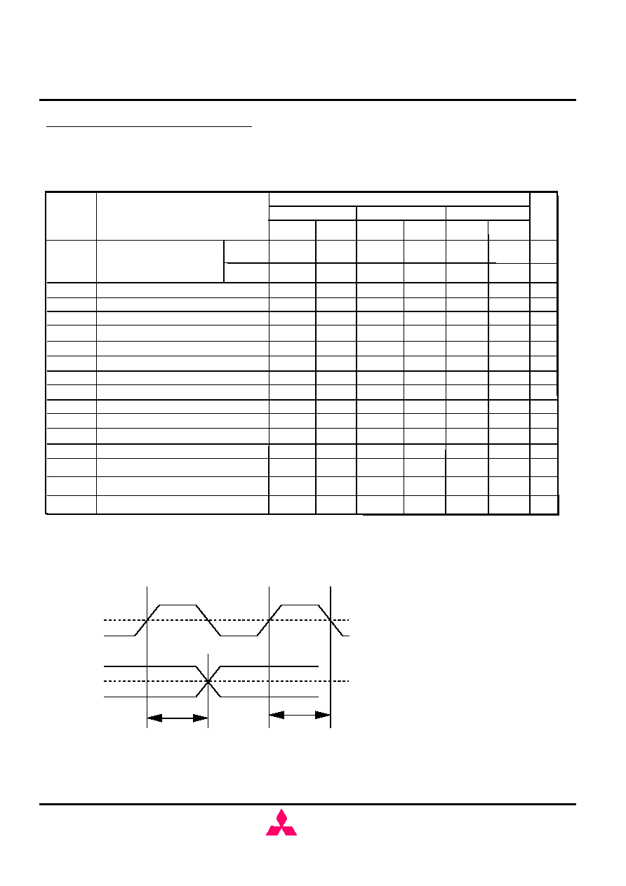
Frequency
CLK Access Time
-8,-8L
100MHz
6.0ns(CL=2)
(Component SDRAM)
6.0ns(CL=3)
100MHz
-7,-7L
5.4ns(CL=3)
-6,-6L
133MHz
MH8S64AQFC -6,-6L,-7,-7L,-8,-8L
536,870,912-BIT (8,388,608 - WORD BY 64-BIT)SynchronousDRAM
MITSUBISHI LSIs
( / 55 )
22.Sep.2000
MIT-DS-0374-0.3
MITSUBISHI
ELECTRIC
Preliminary Spec.
Some contents are subject to change without notice.
2
NC = No Connection
PIN CONFIGURATION
PIN
Number
Front side
Pin Name
Back side
Pin Name
PIN
Number
1
3
5
7
9
11
13
15
17
19
2
4
6
8
10
12
14
16
18
20
PIN
Number
Front side
Pin Name
Back side
Pin Name
PIN
Number
73
74
75
76
77
78
79
80
81
82
83
84
85
86
87
88
89
90
91
92
21
22
93
94
23
24
95
96
25
26
97
98
27
28
99
100
29
30
101
102
31
32
103
104
33
34
105
106
35
36
107
108
37
38
109
110
39
40
111
112
41
42
113
114
43
44
115
116
45
46
117
118
47
48
119
120
49
50
121
122
51
52
123
124
53
54
125
126
55
56
127
128
57
58
129
130
59
60
131
132
61
62
133
134
63
64
135
136
65
66
137
138
67
68
139
140
69
70
141
142
71
72
143
144
Vss
DQ0
DQ1
DQ2
DQ3
Vcc
DQ4
DQ5
DQ6
DQ7
Vss
DQ32
DQ33
DQ34
DQ35
Vcc
DQ36
DQ37
DQ38
DQ39
NC
CLK1
Vss
Vss
NC
NC
NC
NC
Vcc
Vcc
DQ16
DQ48
DQ17
DQ49
DQ18
DQ50
DQ19
DQ51
Vss
Vss
Vss
Vss
DQ20
DQ52
DQMB0
DQMB4
DQ21
DQ53
DQMB1
DQMB5
DQ22
DQ54
Vcc
Vcc
DQ23
DQ55
A0
A3
Vcc
Vcc
A1
A4
A6
A7
A2
A5
A8
BA0
Vss
Vss
Vss
Vss
DQ8
DQ40
A9
BA1
DQ9
DQ41
A10
A11
DQ10
DQ42
Vcc
Vcc
DQ11
DQ43
DQMB2
DQMB6
Vcc
Vcc
DQMB3
DQMB7
DQ12
DQ44
Vss
Vss
DQ13
DQ45
DQ24
DQ56
DQ14
DQ46
DQ25
DQ57
DQ15
DQ47
DQ26
DQ58
Vss
Vss
DQ27
DQ59
NC
NC
Vcc
Vcc
NC
NC
DQ28
DQ60
CLK0
CKE0
DQ29
DQ61
Vcc
Vcc
DQ30
DQ62
/RAS
/CAS
DQ31
DQ63
/WE
CKE1
Vss
Vss
/S0
NC
SDA
SCL
/S1
NC
Vcc
Vcc
MH8S64AQFC -6,-6L,-7,-7L,-8,-8L
536,870,912-BIT (8,388,608 - WORD BY 64-BIT)SynchronousDRAM
MITSUBISHI LSIs
( / 55 )
22.Sep.2000
MIT-DS-0374-0.3
MITSUBISHI
ELECTRIC
Preliminary Spec.
Some contents are subject to change without notice.
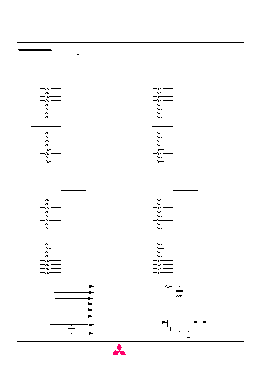
Block Diagram
3
CLK0
SERIAL PD
SCL
SDA
A0
A1
A2
Vcc
Vss
D0 - D3
D0 - D3
/S0
DQMB0
DQMB4
DQMB1
DQMB5
DQMB2
DQMB6
DQMB3
DQMB7
DQ0
DQ1
DQ2
DQ3
DQ4
DQ5
DQ6
DQ7
DQ32
DQ33
DQ34
DQ35
DQ36
DQ37
DQ38
DQ39
DQ8
DQ9
DQ10
DQ11
DQ12
DQ13
DQ14
DQ15
DQ40
DQ41
DQ42
DQ43
DQ44
DQ45
DQ46
DQ47
DQ16
DQ17
DQ18
DQ19
DQ20
DQ21
DQ22
DQ23
DQ48
DQ49
DQ50
DQ51
DQ52
DQ53
DQ54
DQ55
DQ24
DQ25
DQ26
DQ27
DQ28
DQ29
DQ30
DQ31
DQ56
DQ57
DQ58
DQ59
DQ60
DQ61
DQ62
DQ63
CKE0
D0 - D3
/RAS
D0 - D3
/CAS
D0 - D3
/WE
D0 - D3
BA0,BA1,A<11:0>
D0 - D3
CLK1
10
I/O 0
I/O 1
I/O 2
I/O 3
DQML /CS
D0
I/O 4
I/O 5
I/O 6
I/O 7
I/O 8
I/O 9
I/O 10
I/O 11
DQMU
I/O 12
I/O 13
I/O 14
I/O 15
I/O 0
I/O 1
I/O 2
I/O 3
DQML /CS
D2
I/O 4
I/O 5
I/O 6
I/O 7
I/O 8
I/O 9
I/O 10
I/O 11
DQMU
I/O 12
I/O 13
I/O 14
I/O 15
I/O 0
I/O 1
I/O 2
I/O 3
DQML /CS
D1
I/O 4
I/O 5
I/O 6
I/O 7
I/O 8
I/O 9
I/O 10
I/O 11
DQMU
I/O 12
I/O 13
I/O 14
I/O 15
I/O 0
I/O 1
I/O 2
I/O 3
DQML /CS
D3
I/O 4
I/O 5
I/O 6
I/O 7
I/O 8
I/O 9
I/O 10
I/O 11
DQMU
I/O 12
I/O 13
I/O 14
I/O 15
MH8S64AQFC -6,-6L,-7,-7L,-8,-8L
536,870,912-BIT (8,388,608 - WORD BY 64-BIT)SynchronousDRAM
MITSUBISHI LSIs
( / 55 )
22.Sep.2000
MIT-DS-0374-0.3
MITSUBISHI
ELECTRIC
Preliminary Spec.
Some contents are subject to change without notice.
4
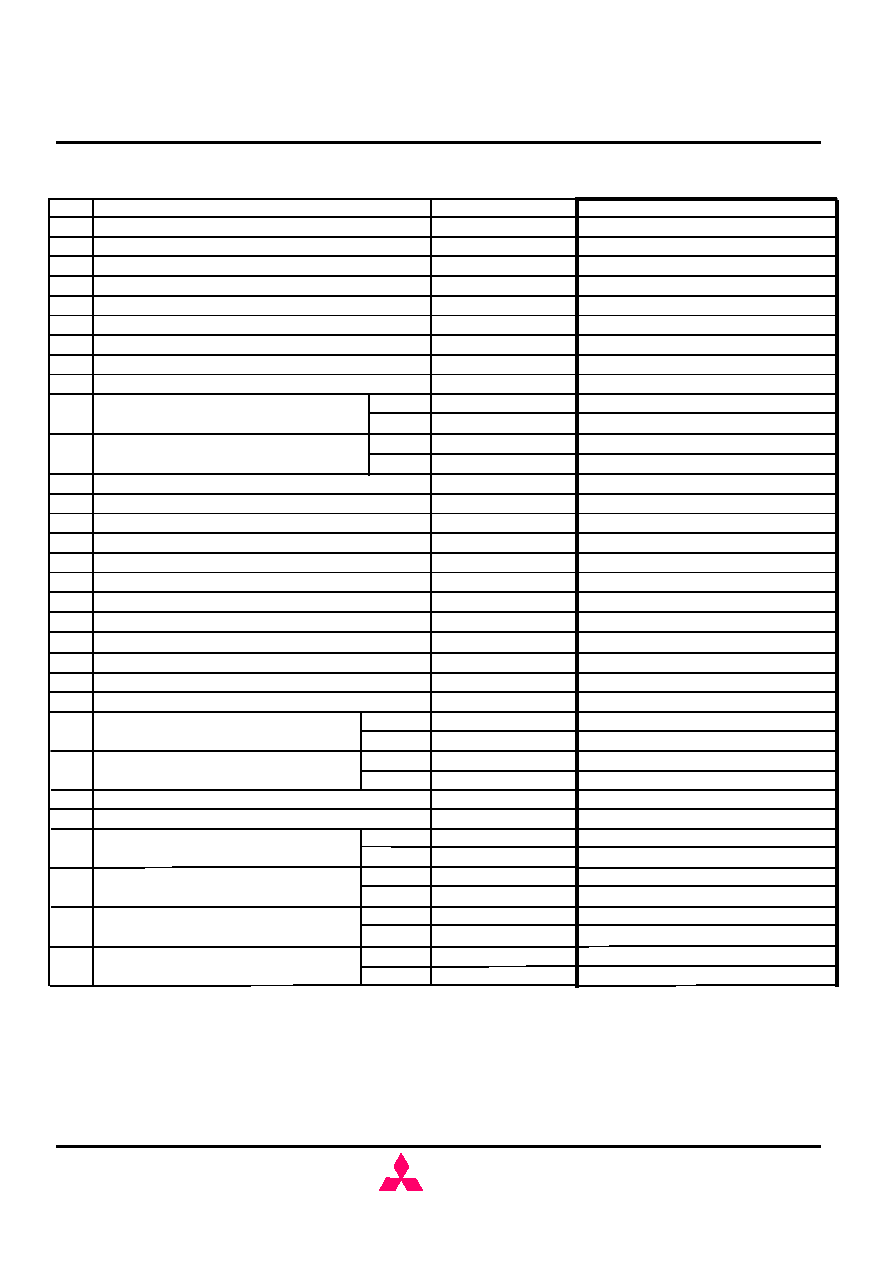
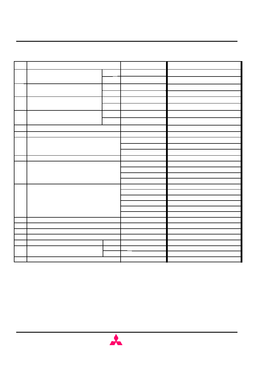
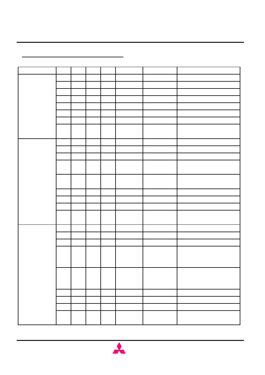
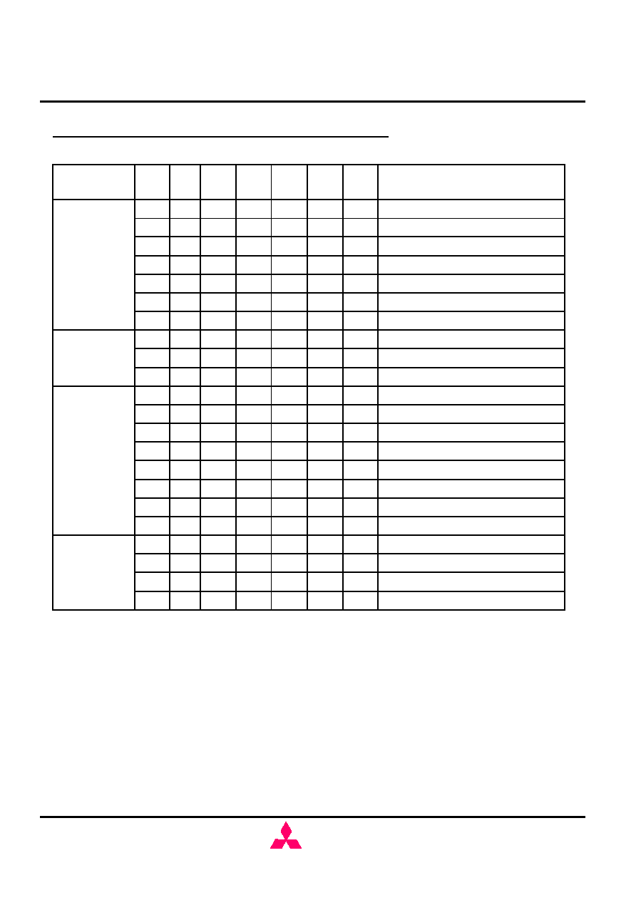
Serial Presence Detect Table I
Byte
Function described
SPD enrty data
SPD DATA(hex)
0
Defines # bytes written into serial memory at module mfgr
128
80
1
Total # bytes of SPD memory device
256 Bytes
08
2
Fundamental memory type
SDRAM
04
3
# Row Addresses on this assembly
A0-A11
0C
4
# Column Addresses on this assembly
A0-A8
09
5
# Module Banks on this assembly
1BANK
01
6
Data Width of this assembly...
x64
40
7
... Data Width continuation
0
00
8
Voltage interface standard of this assembly
LVTTL
01
9
SDRAM Cycletime at Max.Supported CAS Latency (CL).
A0
Cycle time for CL=3
10
SDRAM Access from Clock
6ns
60
tAC for CL=3
11
DIMM Configuration type (Non-parity,Parity,ECC)
Non-PARITY
00
12
Refresh Rate/Type
self refresh(15.625uS)
80
13
SDRAM width,Primary DRAM
x16
10
14
Error Checking SDRAM data width
N/A
00
15
Minimum Clock Delay,Back to Back Random Column Addresses
1
01
16
Burst Lengths Supported
1/2/4/8/Full page
8F
17
# Banks on Each SDRAM device
4bank
04
18
CAS# Latency
2/3
06
19
CS# Latency
0
01
20
Write Latency
0
01
21
SDRAM Module Attributes
non-buffered,non-registered
00
22
SDRAM Device Attributes:General
Precharge All,Auto precharge
0E
23
SDRAM Cycle time(2nd highest CAS latency)
13ns
D0
Cycle time for CL=2
24
SDRAM Access form Clock(2nd highest CAS latency)
7ns
70
tAC for CL=2
25
SDRAM Cycle time(3rd highest CAS latency)
N/A
00
N/A
00
26
SDRAM Access form Clock(3rd highest CAS latency)
10ns
-8,-8L
-8,-8L
10ns
A0
6ns
60
7.5ns
5.4ns
-6,-6L
-7,-7L,-8,-8L
-6,-6L
-7,-7L,-8,-8L
75
54
-6,-6L,-7,-7L
-6,-6L,-7,-7L
27
Precharge to Active Minimum
20ns
14
28
Row Active to Row Active Min.
15ns
0F
29
RAS to CAS Delay Min
22.5ns
17
30
Active to Precharge Min
50ns
32
22.5ns
17
20ns
14
20ns
14
45ns
2D
-6,-6L
-7,-7L,-8,-8L
-6,-6L
-7,-7L,-8,-8L
-6,-6L
-7,-7L,-8,-8L
-6,-6L
-7,-7L,-8,-8L
MH8S64AQFC -6,-6L,-7,-7L,-8,-8L
536,870,912-BIT (8,388,608 - WORD BY 64-BIT)SynchronousDRAM
MITSUBISHI LSIs
( / 55 )
22.Sep.2000
MIT-DS-0374-0.3
MITSUBISHI
ELECTRIC
Preliminary Spec.
Some contents are subject to change without notice.
5
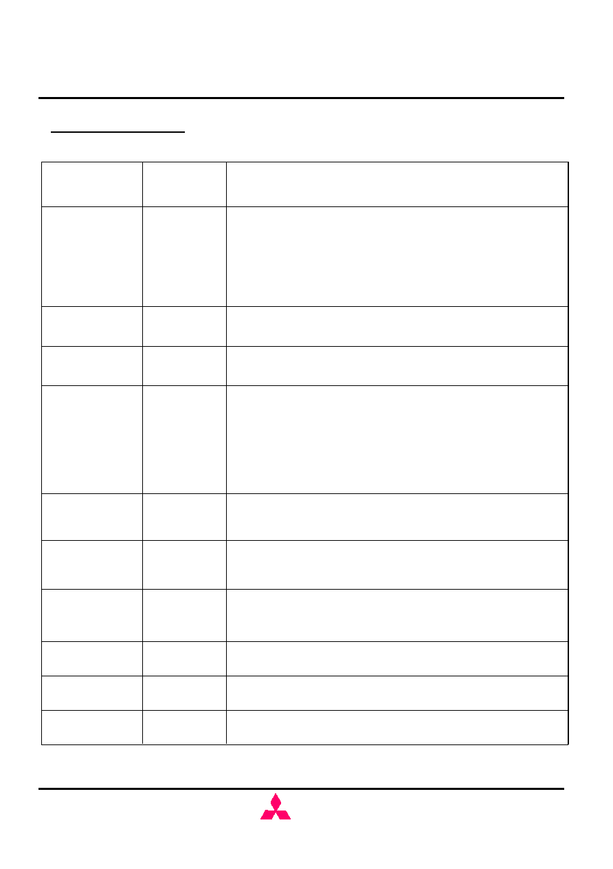
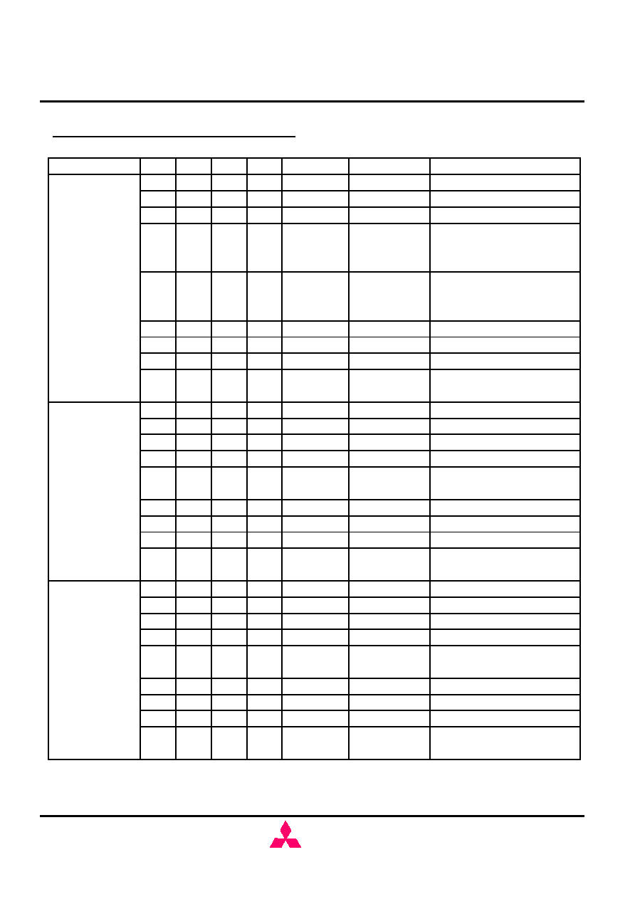
Serial Presence Detect Table II
31
Density of each bank on module
64MByte
10
36-61
Superset Information (may be used in future)
option
00
62
SPD Revision
63
Checksum for bytes 0-62
Check sum for -8,-8L
4D
64-71
Manufactures Jedec ID code per JEP-108E
MITSUBISHI
1CFFFFFFFFFFFFFF
72
Manufacturing location
Miyoshi,Japan
01
Tajima,Japan
02
NC,USA
03
Germany
04
73-90
Manufactures Part Number
MH8S64AQFC-8
MH8S64AQFC-8L
91-92
Revision Code
PCB revision
rrrr
93-94
Manufacturing date
year/week code
yyww
95-98
Assembly Serial Number
serial number
ssssssss
99-125
Manufacture Specific Data
option
00
126
Intetl specification frequency
100MHz
64
127
Intel specification CAS# Latency support
128+
Unused storage locations
open
00
32
Command and Address signal input setup time
33
Command and Address signal input hold time
34
Data signal input setup time
35
Data signal input hold time
rev 1.2B
12
Check sum for -7,-7L
0D
MH8S64AQFC-7
4D4838533634415146432D37202020202020
-6,-6L,-7,7L
8F
-8,8L
8D
MH8S64AQFC-7L
4D4838533634415146432D374C2020202020
4D4838533634415146432D38202020202020
4D4838533634415146432D384C2020202020
20
20
10
10
15
08
15
08
2ns
1ns
2ns
1ns
1.5ns
0.8ns
1.5ns
0.8ns
Check sum for -6,-6L
AC
MH8S64AQFC-6
MH8S64AQFC-6L
-6,-6L
-7,-7L,-8,-8L
-6,-6L
-7,-7L,-8,-8L
-6,-6L
-7,-7L,-8,-8L
-6,-6L
-7,-7L,-8,-8L
CL=2/3,AP,CK0,1
CL=3,AP,CK0,1
4D4838533634415146432D364C2020202020
4D4838533634415146432D36202020202020
MH8S64AQFC -6,-6L,-7,-7L,-8,-8L
536,870,912-BIT (8,388,608 - WORD BY 64-BIT)SynchronousDRAM
MITSUBISHI LSIs
( / 55 )
22.Sep.2000
MIT-DS-0374-0.3
MITSUBISHI
ELECTRIC
Preliminary Spec.
Some contents are subject to change without notice.
PIN FUNCTION
Input
Master Clock:All other inputs are referenced to the rising
edge of CK
CKE0
Input
Clock Enable:CKE controls internal clock.When CKE is
low,internal clock for the following cycle is ceased. CKE is
also used to select auto / self refresh. After self refresh
mode is started, CKE E becomes asynchronous input.Self
refresh is maintained as long as CKE is low.
/S0
Input
Chip Select: When /S is high,any command means
No Operation.
/RAS,/CAS,/WE
Input
Combination of /RAS,/CAS,/WE defines basic commands.
A0-11
Input
A0-11 specify the Row/Column Address in conjunction with
BA0,1.The Row Address is specified by A0-11.The Column
Address is specified by A0-8.A10 is also used to indicate
precharge option.When A10 is high at a read / write
command, an auto precharge is performed. When A10 is
high at a precharge command, both banks are precharged.
BA0,1
Input
Bank Address:BA0,1 is not simply BA.BA specifies the
bank to which a command is applied.BA0,1 must be set
with ACT,PRE,READ,WRITE commands
DQ0-63
Input/Output Data In and Data out are referenced to the rising edge
of CK
DQMB0-7
Input
Din Mask/Output Disable:When DQMB is high in burst
write.Din for the current cycle is masked.When DQMB is
high in burst read,Dout is disabled at the next but one cycle.
Vdd,Vss
Power Supply Power Supply for the memory mounted module.
SCL
SDA
Input
Output
Serial clock for serial PD
Serial data for serial PD
6
CLK0
MH8S64AQFC -6,-6L,-7,-7L,-8,-8L
536,870,912-BIT (8,388,608 - WORD BY 64-BIT)SynchronousDRAM
MITSUBISHI LSIs
( / 55 )
22.Sep.2000
MIT-DS-0374-0.3
MITSUBISHI
ELECTRIC
Preliminary Spec.
Some contents are subject to change without notice.
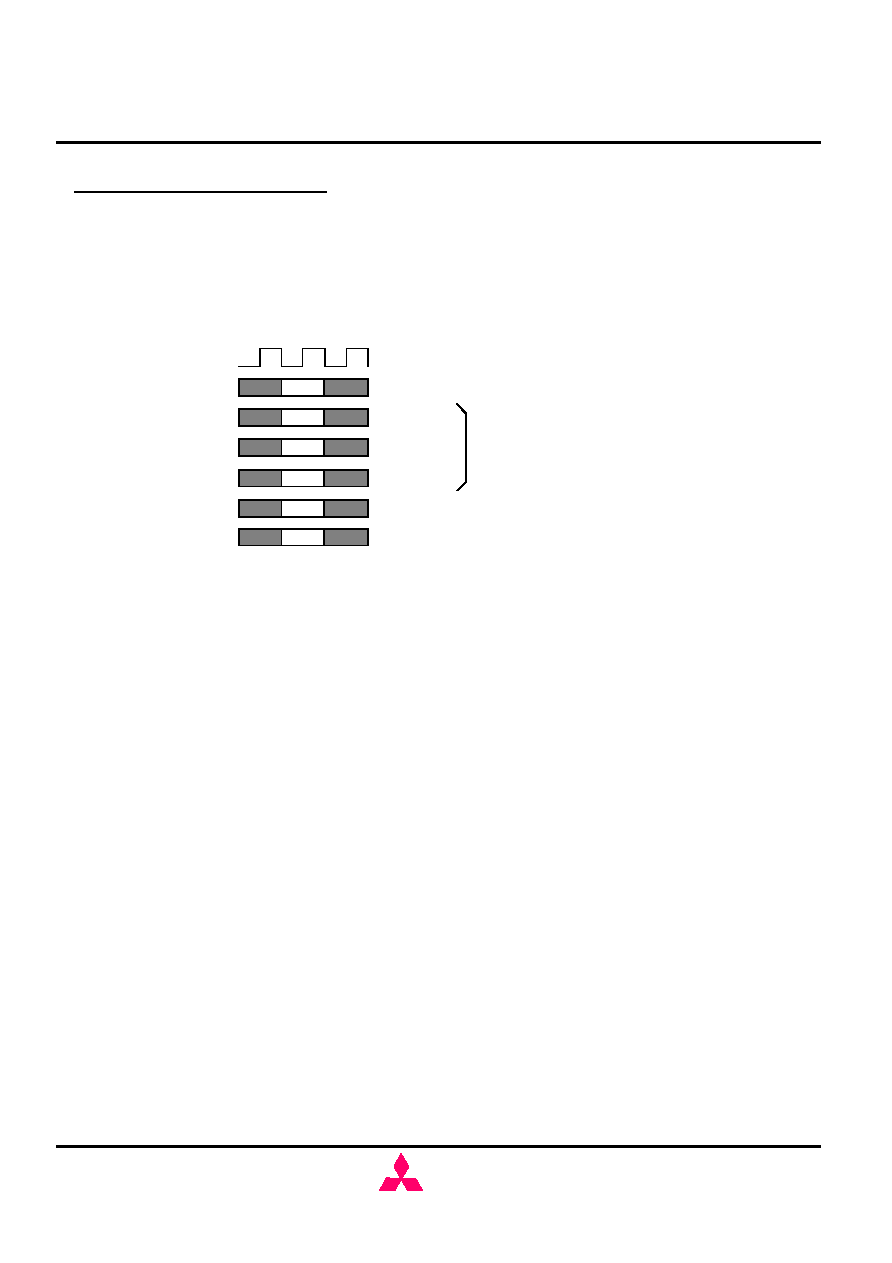
BASIC FUNCTIONS
/S
Chip Select : L=select, H=deselect
/RAS
Command
/CAS
Command
/WE
Command
CKE
Ref resh Option @ref resh
command
A10
Precharge Option @precharge or read/write
command
CK
def ine basic commands
The MH8S64AQFC provides basic functions ,bank(row)activate,burst read / write,
bank(row)precharge,and auto / self refresh.
Each command is defined by control s ignals of /RAS,/CAS and /WE at CK rising edge.
In addition to 3 s ignals,/S,CKE and A10 are used as chip select,refresh option,and
precharge option,respectively.
To know the detailed definition of commands please see the command truth table.
Activate(ACT) [/RAS =L, /CAS = /WE =H]
Read(READ) [/RAS =H,/CAS =L, /WE =H]
Write(WRITE) [/RAS =H, /CAS = /WE =L]
Precharge(PRE) [/RAS =L, /CAS =H,/WE =L]
Auto-Refresh(REFA) [/RAS =/CAS =L, /WE =CKE =H]
ACT command activates a row in an idle bank indicated by BA.
READ command starts burst read from the active bank indicated by BA.Firs t output
data appears after /CAS latency. When A10 =H at this command,the bank is
deactivated after the burst read(auto-precharge,
READA).
WRITE command starts burst write to the active bank indicated by BA. Total data
length to be written is set by burst length. When A10 =H at this command, the bank is
deactivated after the burst write(auto-precharge,
WRITEA).
PRE command deactivates the active bank indicated by BA. This command also
term inates burst read / write operation. When A10 =H at this command, both banks
are deactivated(precharge all,
PREA).
PEFA command starts auto-refresh cycle. Refresh address including bank address
are generated internally. After this command, the banks are precharged automatically.
7
MH8S64AQFC -6,-6L,-7,-7L,-8,-8L
536,870,912-BIT (8,388,608 - WORD BY 64-BIT)SynchronousDRAM
MITSUBISHI LSIs
( / 55 )
22.Sep.2000
MIT-DS-0374-0.3
MITSUBISHI
ELECTRIC
Preliminary Spec.
Some contents are subject to change without notice.
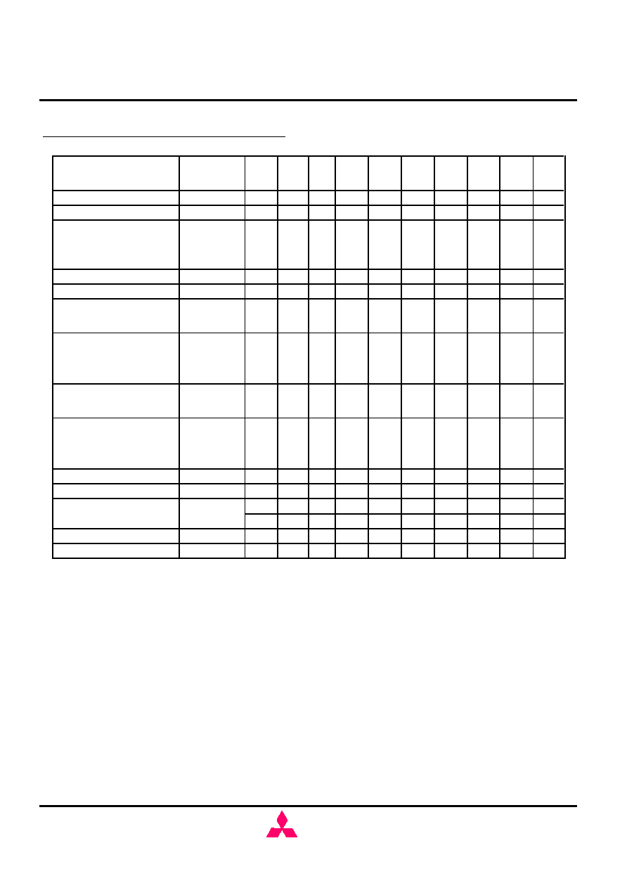
H =High Level, L = Low Level, V = Valid, X = Don't Care, n = CK cycle number
NOTE:
1.A7-9 = 0, A0-6 = Mode Address
8
COMMAND TRUTH TABLE
COMMAND
MNEMONIC
CKE
n-1
CKE
n
/S
/RAS /CAS
/WE BA0,1
A10
A0-9
Deselect
DESEL
H
X
H
X
X
X
X
X
X
No Operation
NOP
H
X
L
H
H
H
X
X
X
Row Adress Entry &
Bank Activate
ACT
H
X
L
L
H
H
V
V
V
Single Bank Precharge
PRE
H
X
L
L
H
L
V
L
X
Precharge All Bank
PREA
H
X
L
L
H
L
X
H
X
Column Address Entry
& Write
WRIT E
H
X
L
H
L
L
V
L
V
Column Address Entry
& Write with Auto-
Precharge
WRITEA
H
X
L
H
L
L
V
H
V
Column Address Entry
& Read
READ
H
X
L
H
L
H
V
L
V
Column Address Entry
& Read with Auto
Precharge
READA
H
X
L
H
L
H
V
H
V
Auto-Refresh
REFA
H
H
L
L
L
H
X
X
X
Self-Refresh Entry
REFS
H
L
L
L
L
H
X
X
X
Self-Refresh Exit
REFSX
L
H
H
X
X
X
X
X
X
L
H
L
H
H
H
X
X
X
Burst Terminate
TERM
H
X
L
H
H
L
X
X
X
Mode Register Set
MRS
H
X
L
L
L
L
L
L
V*1
A11
X
X
V
X
X
V
V
V
V
X
X
X
X
X
L
MH8S64AQFC -6,-6L,-7,-7L,-8,-8L
536,870,912-BIT (8,388,608 - WORD BY 64-BIT)SynchronousDRAM
MITSUBISHI LSIs
( / 55 )
22.Sep.2000
MIT-DS-0374-0.3
MITSUBISHI
ELECTRIC
Preliminary Spec.
Some contents are subject to change without notice.
Current State
/S
/RAS /CAS
/WE
Address
Command
Action
IDLE
H
X
X
X
X
DESEL
NOP
L
H
H
H
X
NOP
NOP
L
H
H
L
BA
TBST
ILLEGAL*2
L
H
L
X
BA,CA,A10
READ/WRITE ILLEGAL*2
L
L
H
H
BA,RA
ACT
Bank Active,Latch RA
L
L
H
L
BA,A10
PRE/PREA
NOP*4
L
L
L
H
X
REFA
Auto-Refresh*5
L
L
L
L
Op-Code,
Mode-Add
MRS
Mode Register Set*5
ROW ACTIVE
H
X
X
X
X
DESEL
NOP
L
H
H
H
X
NOP
NOP
L
H
H
L
BA
TBST
NOP
L
H
L
H
BA,CA,A10
READ/READA
Begin Read,Latch CA,
Determine Auto-Precharge
L
H
L
L
BA,CA,A10
WRITE/
WRITEA
Begin Write,Latch CA,
Determine Auto-Precharge
L
L
H
H
BA,RA
ACT
Bank Active/ILLEGAL*2
L
L
H
L
BA,A10
PRE/PREA
Precharge/Precharge All
L
L
L
H
X
REFA
ILLEGAL
L
L
L
L
Op-Code,
Mode-Add
MRS
ILLEGAL
READ
H
X
X
X
X
DESEL
NOP(Continue Burst to END)
L
H
H
H
X
NOP
NOP(Continue Burst to END)
L
H
H
L
BA
TBST
Terminate Burst
L
H
L
H
BA,CA,A10
READ/READA
Terminate Burst,Latch CA,
Begin New Read,Determine
Auto-Precharge*3
L
H
L
L
BA,CA,A10 WRITE/WRITEA
Terminate Burst,Latch CA,
Begin Write,Determine Auto-
Precharge*3
L
L
H
H
BA,RA
ACT
Bank Active/ILLEGAL*2
L
L
H
L
BA,A10
PRE/PREA
Terminate Burst,Precharge
L
L
L
H
X
REFA
ILLEGAL
L
L
L
L
Op-Code,
Mode-Add
MRS
ILLEGAL
FUNCTION TRUTH TABLE
9
MH8S64AQFC -6,-6L,-7,-7L,-8,-8L
536,870,912-BIT (8,388,608 - WORD BY 64-BIT)SynchronousDRAM
MITSUBISHI LSIs
( / 55 )
22.Sep.2000
MIT-DS-0374-0.3
MITSUBISHI
ELECTRIC
Preliminary Spec.
Some contents are subject to change without notice.
FUNCTION TRUTH TABLE(continued)
Current State
/S
/RAS /CAS
/WE
Address
Command
Action
WRIT E
H
X
X
X
X
DESEL
NOP(Continue Burst to END)
L
H
H
H
X
NOP
NOP(Continue Burst to END)
L
H
H
L
BA
TBST
Terminate Burst
L
H
L
H
BA,CA,A10
READ/READA
Terminate Burst,Latch CA,
Begin Read,Determine Auto-
Precharge*3
L
H
L
L
BA,CA,A10
WRITE/
WRITEA
Terminate Burst,Latch CA,
Begin Write,Determine Auto-
Precharge*3
L
L
H
H
BA,RA
ACT
Bank Active/ILLEGAL*2
L
L
H
L
BA,A10
PRE/PREA
Terminate Burst,Precharge
L
L
L
H
X
REFA
ILLEGAL
L
L
L
L
Op-Code,
Mode-Add
MRS
ILLEGAL
READ with
H
X
X
X
X
DESEL
NOP(Continue Burst to END)
AUT O
L
H
H
H
X
NOP
NOP(Continue Burst to END)
PRECHARGE
L
H
H
L
BA
TBST
ILLEGAL
L
H
L
H
BA,CA,A10
READ/READA ILLEGAL
L
H
L
L
BA,CA,A10
WRITE/
WRITEA
ILLEGAL
L
L
H
H
BA,RA
ACT
Bank Active/ILLEGAL*2
L
L
H
L
BA,A10
PRE/PREA
ILLEGAL*2
L
L
L
H
X
REFA
ILLEGAL
L
L
L
L
Op-Code,
Mode-Add
MRS
ILLEGAL
WRITE with
H
X
X
X
X
DESEL
NOP(Continue Burst to END)
AUT O
L
H
H
H
X
NOP
NOP(Continue Burst to END)
PRECHARGE
L
H
H
L
BA
TBST
ILLEGAL
L
H
L
H
BA,CA,A10
READ/READA ILLEGAL
L
H
L
L
BA,CA,A10
WRITE/
WRITEA
ILLEGAL
L
L
H
H
BA,RA
ACT
Bank Active/ILLEGAL*2
L
L
H
L
BA,A10
PRE/PREA
ILLEGAL*2
L
L
L
H
X
REFA
ILLEGAL
L
L
L
L
Op-Code,
Mode-Add
MRS
ILLEGAL
10
MH8S64AQFC -6,-6L,-7,-7L,-8,-8L
536,870,912-BIT (8,388,608 - WORD BY 64-BIT)SynchronousDRAM
MITSUBISHI LSIs
( / 55 )
22.Sep.2000
MIT-DS-0374-0.3
MITSUBISHI
ELECTRIC
Preliminary Spec.
Some contents are subject to change without notice.
FUNCTION TRUTH TABLE(continued)
Current State
/S
/RAS
/CAS
/WE
Address
Command
Action
PRE -
H
X
X
X
X
DESEL
NOP(Idle after tRP)
CHARGING
L
H
H
H
X
NOP
NOP(Idle after tRP)
L
H
H
L
BA
TBST
ILLEGAL*2
L
H
L
X
BA,CA,A10
READ/WRITE ILLEGAL*2
L
L
H
H
BA,RA
ACT
ILLEGAL*2
L
L
H
L
BA,A10
PRE/PREA
NOP*4(Idle after tRP)
L
L
L
H
X
REFA
ILLEGAL
L
L
L
L
Op-Code,
Mode-Add
MRS
ILLEGAL
ROW
H
X
X
X
X
DESEL
NOP(Row Active after tRCD
ACT IVATING
L
H
H
H
X
NOP
NOP(Row Active after tRCD
L
H
H
L
BA
TBST
ILLEGAL*2
L
H
L
X
BA,CA,A10
READ/WRITE ILLEGAL*2
L
L
H
H
BA,RA
ACT
ILLEGAL*2
L
L
H
L
BA,A10
PRE/PREA
ILLEGAL*2
L
L
L
H
X
REFA
ILLEGAL
L
L
L
L
Op-Code,
Mode-Add
MRS
ILLEGAL
WRITE RE-
H
X
X
X
X
DESEL
NOP
COVERING
L
H
H
H
X
NOP
NOP
L
H
H
L
BA
TBST
ILLEGAL*2
L
H
L
X
BA,CA,A10
READ/WRITE ILLEGAL*2
L
L
H
H
BA,RA
ACT
ILLEGAL*2
L
L
H
L
BA,A10
PRE/PREA
ILLEGAL*2
L
L
L
H
X
REFA
ILLEGAL
L
L
L
L
Op-Code,
Mode-Add
MRS
ILLEGAL
11
MH8S64AQFC -6,-6L,-7,-7L,-8,-8L
536,870,912-BIT (8,388,608 - WORD BY 64-BIT)SynchronousDRAM
MITSUBISHI LSIs
( / 55 )
22.Sep.2000
MIT-DS-0374-0.3
MITSUBISHI
ELECTRIC
Preliminary Spec.
Some contents are subject to change without notice.
FUNCTION TRUTH TABLE(continued)
Current State
/S
/RAS /CAS
/WE
Address
Command
Action
RE-
H
X
X
X
X
DESEL
NOP(Idle after tRC)
FRESHING
L
H
H
H
X
NOP
NOP(Idle after tRC)
L
H
H
L
BA
TBST
ILLEGAL
L
H
L
X
BA,CA,A10
READ/WRITE ILLEGAL
L
L
H
H
BA,RA
ACT
ILLEGAL
L
L
H
L
BA,A10
PRE/PREA
ILLEGAL
L
L
L
H
X
REFA
ILLEGAL
L
L
L
L
Op-Code,
Mode-Add
MRS
ILLEGAL
MODE
H
X
X
X
X
DESEL
NOP(Idle after tRSC)
REGISTER
L
H
H
H
X
NOP
NOP(Idle after tRSC)
SETTING
L
H
H
L
BA
TBST
ILLEGAL
L
H
L
X
BA,CA,A10
READ/WRITE ILLEGAL
L
L
H
H
BA,RA
ACT
ILLEGAL
L
L
H
L
BA,A10
PRE/PREA
ILLEGAL
L
L
L
H
X
REFA
ILLEGAL
L
L
L
L
Op-Code,
Mode-Add
MRS
ILLEGAL
ABBREVIATIONS:
H = Hige Level, L = Low Level, X = Don't Care
BA = Bank Address , RA = Row Address, CA = Column Address, NOP = No Operation
NOTES:
1. All entries assume that CKE was High during the preceding clock cycle and the current
clock cycle.
2. ILLEGAL to bank in specified state; function may be legal in the bank indicated by BA,
depending on the state of that bank.
3. Mus t satisfy bus contention, bus turn around, write recovery requirements.
4. NOP to bank precharging or in idle state.May precharge bank indicated by BA.
5. ILLEGAL if any bank is not idle.
ILLEGAL = Device operation and / or date-integrity are not guaranteed.
12
MH8S64AQFC -6,-6L,-7,-7L,-8,-8L
536,870,912-BIT (8,388,608 - WORD BY 64-BIT)SynchronousDRAM
MITSUBISHI LSIs
( / 55 )
22.Sep.2000
MIT-DS-0374-0.3
MITSUBISHI
ELECTRIC
Preliminary Spec.
Some contents are subject to change without notice.
FUNCTION TRUTH TABLE FOR CKE
Current State
CK
n-1
CK
n
/S
/RAS /CAS
/WE
Add
Action
SELF -
H
X
X
X
X
X
X
INVALID
REFRESH*1
L
H
H
X
X
X
X
Exit Self-Refresh(Idle after tRC)
L
H
L
H
H
H
X
Exit Self-Refresh(Idle after tRC)
L
H
L
H
H
L
X
ILLEGAL
L
H
L
H
L
X
X
ILLEGAL
L
H
L
L
X
X
X
ILLEGAL
L
L
X
X
X
X
X
NOP(Maintain Self-Refresh)
POWER
H
X
X
X
X
X
X
INVALID
DOWN
L
H
X
X
X
X
X
Exit Power Down to Idle
L
L
X
X
X
X
X
NOP(Maintain Self-Refresh)
ALL BANKS
H
H
X
X
X
X
X
Refer to Function Truth Table
IDLE*2
H
L
L
L
L
H
X
Enter Self-Refresh
H
L
H
X
X
X
X
Enter Power Down
H
L
L
H
H
H
X
Enter Power Down
H
L
L
H
H
L
X
ILLEGAL
H
L
L
H
L
X
X
ILLEGAL
H
L
L
L
X
X
X
ILLEGAL
L
X
X
X
X
X
X
Refer to Current State = Power Down
ANY STATE
H
H
X
X
X
X
X
Refer to Function Truth Table
other than
H
L
X
X
X
X
X
Begin CK0 Suspend at Next Cycle*3
listed above
L
H
X
X
X
X
X
Exit CK0 Suspend at Next Cycle*3
L
L
X
X
X
X
X
Maintain CK0 Suspend
ABBREVIATIONS:
H = High Level, L = Low Level, X = Don't Care
NOTES:
1. CKE Low to High transition will re-enable CK and other inputs
asynchronously.
A minimum setup time must be satisfied before any command other than EXIT.
2. Power-Down and Self-Refresh can be entered only form the All banks idle State.
3. Mus t be legal command.
13
MH8S64AQFC -6,-6L,-7,-7L,-8,-8L
536,870,912-BIT (8,388,608 - WORD BY 64-BIT)SynchronousDRAM
MITSUBISHI LSIs
( / 55 )
22.Sep.2000
MIT-DS-0374-0.3
MITSUBISHI
ELECTRIC
Preliminary Spec.
Some contents are subject to change without notice.
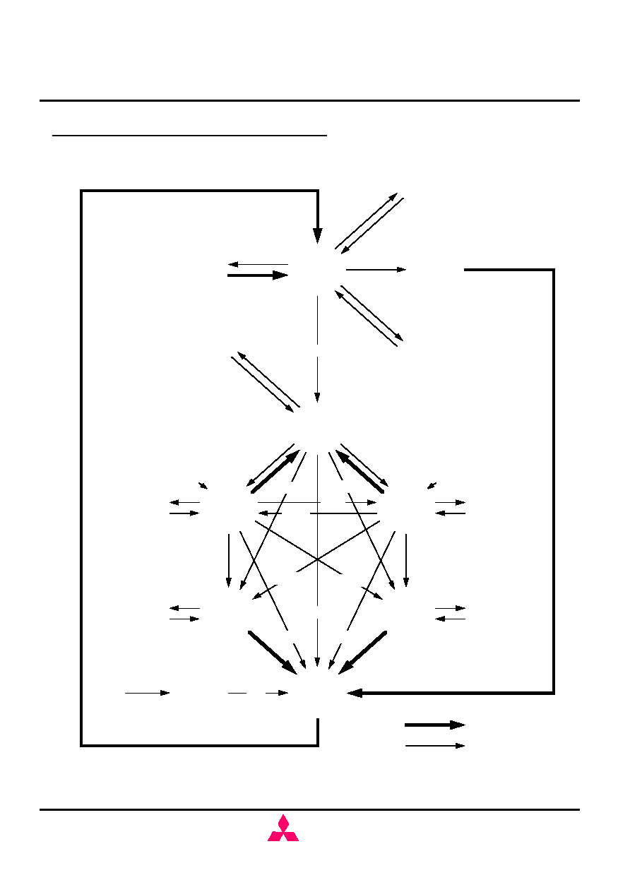
SIMPLIFIED STATE DIAGRAM
ROW
ACTIVE
IDLE
PRE
CHARGE
AUTO
REFRESH
SELF
REFRESH
MODE
REGISTER
SET
POWER
DOWN
READ
READA
WRITE
WRITEA
READ
SUSPEND
READA
SUSPEND
WRITE
SUSPEND
WRITEA
SUSPEND
POWER
ON
CLK
SUSPEND
CKEL
CKEH
CKEL
CKEH
CKEL
CKEH
CKEL
CKEH
ACT
REFA
REFS
REFSX
CKEL
CKEH
MRS
CKEL
CKEH
WRITE
READ
WRITEA
WRITEA
READA
WRITE
READ
PRE
READA
WRITEA
READA
PRE
PRE
PRE
POWER
APPLIED
Automatic Sequence
Command Sequence
14
MH8S64AQFC -6,-6L,-7,-7L,-8,-8L
536,870,912-BIT (8,388,608 - WORD BY 64-BIT)SynchronousDRAM
MITSUBISHI LSIs
( / 55 )
22.Sep.2000
MIT-DS-0374-0.3
MITSUBISHI
ELECTRIC
Preliminary Spec.
Some contents are subject to change without notice.
POWER ON SEQUENCE
Before starting normal operation, the following power on sequence is necessary to prevent
a SDRAM from damaged or malfunctioning.
1. Apply power and start clock.Attempt to maintain CKE high,DQM0-7 high and NOP
condition at the inputs .
2. Maintain stable power, s table cock, and NOP input conditions for a m inimum of 200us.
3. Issue precharge commands for all banks. (PRE or PREA)
4. After all banks become idle state (after tRP), issue 8 or more auto-refresh commands.
5. Issue a mode register set command to initialize the mode register.
After these sequence, the SDRAM is idle state and ready for normal operation.
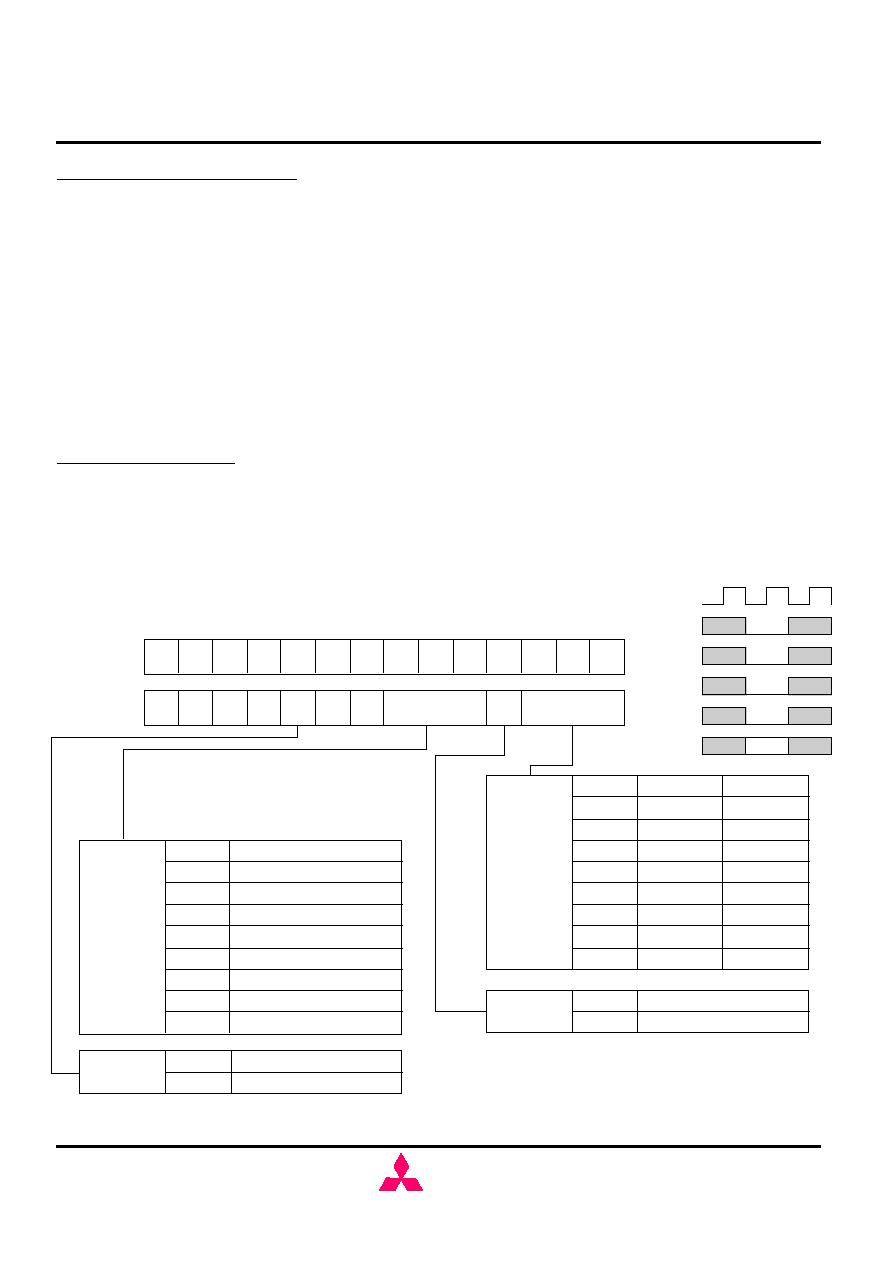
MODE REGISTER
Burst Length, Burs t Type and /CAS Latency can be programmed by setting the mode
register(MRS). The mode register stores these date until the next MRS command, which
may be issued when both banks are in idle state. After tRSC from a MRS command, the
SDRAM is ready for new command.
15
R:Reserved for Future Use
/S
/RAS
/CAS
/WE
BA0,1 A11-0
CK
V
BL
0 0 0
0 0 1
0 1 0
0 1 1
1 0 0
1 0 1
1 1 0
1 1 1
BURST
LENGTH
BT= 0
BT= 1
1
2
4
8
R
R
R
FP
1
2
4
8
R
R
R
R
0
1
BURST
TYPE
SEQUENTIAL
INTERLEAVED
A11 A10 A9
A8
A7
A6
A5
A4
A3
A2
A1
A0
BA1
BA0
0
0
WM
0
0
LTMODE
BT
BL
0
0
CL
0 0 0
0 0 1
0 1 0
0 1 1
1 0 0
1 0 1
1 1 0
1 1 1
LATENCY
MODE
/CAS LATENCY
2
3
R
R
R
R
R
R
0
1
WRIT E
MODE
BURST
SINGLE BIT
FP: Full Page
MH8S64AQFC -6,-6L,-7,-7L,-8,-8L
536,870,912-BIT (8,388,608 - WORD BY 64-BIT)SynchronousDRAM
MITSUBISHI LSIs
( / 55 )
22.Sep.2000
MIT-DS-0374-0.3
MITSUBISHI
ELECTRIC
Preliminary Spec.
Some contents are subject to change without notice.
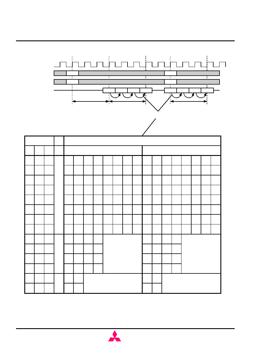
Command
Address
CK
Read
Y
Q0
Q1
Q2
Q3
Write
Y
D0
D1
D2
D3
/CAS Latency
Burst Length
Burst Length
DQ
Burst Type
CL= 3
BL= 4
A2
A1
A0
Initial Address
BL
Sequential
Interleaved
Column Addressing
0
0
0
0
0
1
0
1
0
0
1
1
1
0
0
1
0
1
1
1
0
1
1
1
-
0
0
-
0
1
-
1
0
-
1
1
-
-
0
0
1
2
3
4
5
6
7
0
1
2
3
4
5
6
7
1
2
3
4
5
6
7
0
1
0
3
2
5
4
7
6
2
3
4
5
6
7
0
1
2
3
0
1
6
7
4
5
3
4
5
6
7
0
1
2
3
2
1
0
7
6
5
4
4
5
6
7
0
1
2
3
4
5
6
7
0
1
2
3
5
6
7
0
1
2
3
4
5
4
7
6
1
0
3
2
6
7
0
1
2
3
4
5
6
7
4
5
2
3
0
1
7
0
1
2
0
1
2
3
1
2
3
0
2
3
0
1
3
0
0
1
7
6
5
4
0
1
2
3
1
0
3
2
2
3
0
1
3
2
0
1
-
-
1
1
2
1
0
3
4
5
6
3
2
1
0
1
0
1
0
8
4
2
16
MH8S64AQFC -6,-6L,-7,-7L,-8,-8L
536,870,912-BIT (8,388,608 - WORD BY 64-BIT)SynchronousDRAM
MITSUBISHI LSIs
( / 55 )
22.Sep.2000
MIT-DS-0374-0.3
MITSUBISHI
ELECTRIC
Preliminary Spec.
Some contents are subject to change without notice.
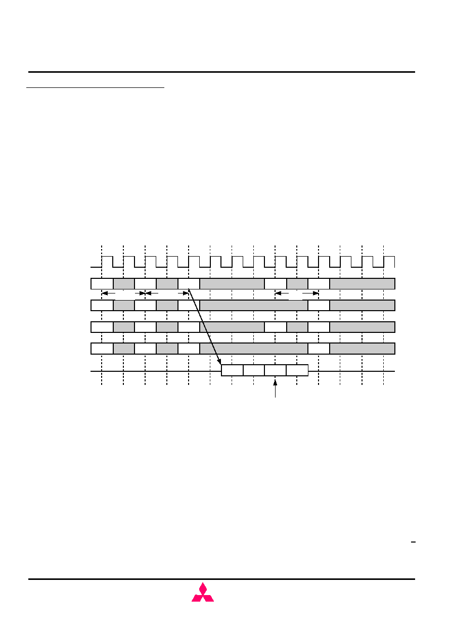
Bank Activation and Precharge All (BL=4, CL=2)
CK
Command
A0-9,11
A10
BA0,1
DQ
ACT
Xa
Xa
00
READ
Y b
0
01
Qa0
Qa1
Qa2
Qa3
ACT
Xb
Xb
01
PRE
tRRD
tRCD
1
ACT
Xa
Xa
00
Precharge all
tRP
OPERATION DESCRIPTION
17
BANK ACTIVATE
One of four banks is activated by an ACT command.
An bank is selected by BA0-1. A row is selected by A0-11.
Multiple banks can be active state concurrently by issuing multiple ACT commands.
Minimum activation interval between one bank and another bank is tRRD.
PRECHARGE
An open bank is deactivated by a PRE command.
A bank to be deactivated is designated by BA0-1.
When multiple banks are active, a precharge all command (PREA, PRE + A10=H)
deactivates all of open banks at the same time. BA0-1 are "Don't Care" in this case.
Minimum delay time of an ACT command after a PRE command to the same bank is tRP.
READ
A READ command can be issued to any active bank. The start address is specified by A0-8
(x16) . 1s t output data is available after the /CAS Latency from the READ. The consecutive
data length is defined by the Burst Length. The address sequence of the burst data is
defined by the Burs t Type. Minimum delay time of a READ command after an ACT command
to the same bank is tRCD.
When A10 is high at a READ command, auto-precharge (READA) is performed. Any
command (READ, WRITE, PRE, ACT, TBST) to the same bank is inhibited till the internal
precharge is complete. The internal precharge starts at the BL after READA. The next ACT
command can be issued after (BL + tRP) from the previous READA. In any case, tRCD+BL >
tRASmin must be met.
MH8S64AQFC -6,-6L,-7,-7L,-8,-8L
536,870,912-BIT (8,388,608 - WORD BY 64-BIT)SynchronousDRAM
MITSUBISHI LSIs
( / 55 )
22.Sep.2000
MIT-DS-0374-0.3
MITSUBISHI
ELECTRIC
Preliminary Spec.
Some contents are subject to change without notice.
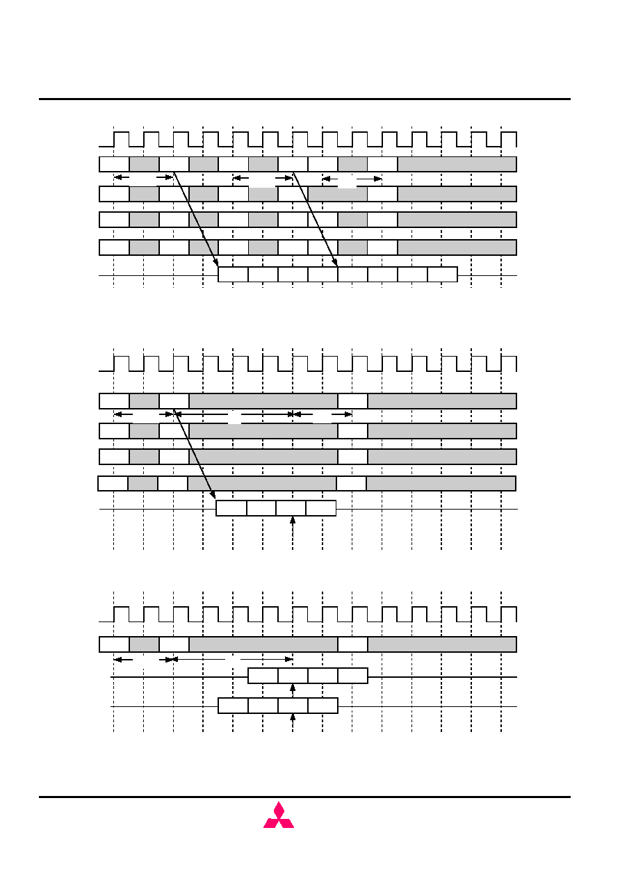
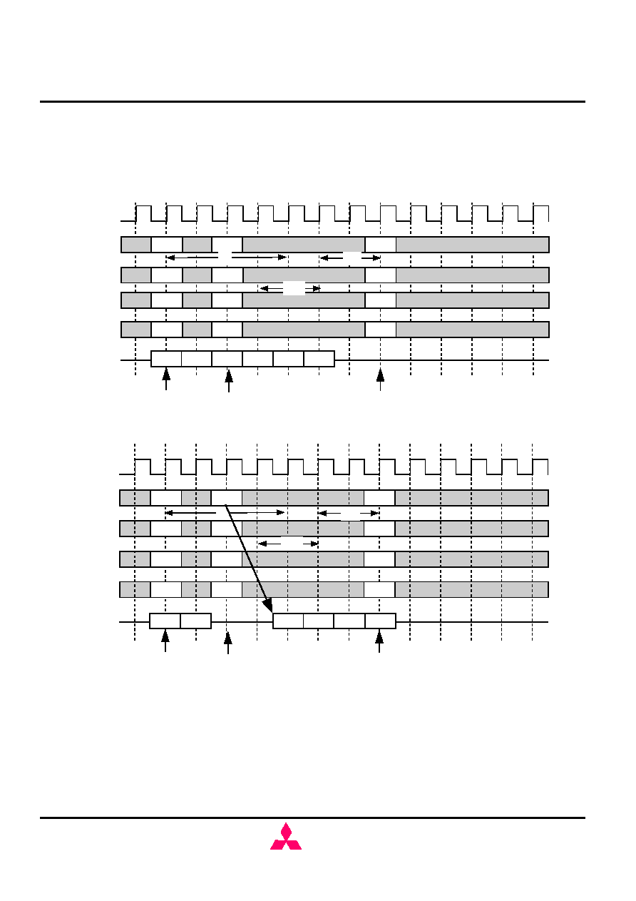
Multi Bank Interleaving READ (BL=4, CL=2)
CK
Command
A0-9, 11
A10
BA0,1
DQ
ACT
Xa
Xa
00
READ
Y a
0
00
READ
Y b
0
01
Qa0
Qa1
Qa2
Qa3
Qb0
Qb1
Qb2
ACT
Xb
Xb
01
PRE
0
00
tRCD
READ with Auto-Precharge (BL=4, CL=2)
CK
Command
A10
DQ
ACT
Xa
Xa
00
READ
Y a
1
00
Qa0
Qa1
Qa2
Qa3
ACT
Xa
Xa
00
Internal precharge starts
tRCD
tRP
Auto-Precharge Timing (READ BL=4)
CK
Command
ACT
READ
Internal precharge starts
DQ
Qa0
Qa1
Qa2
Qa3
DQ
Qa0
Qa1
Qa2
Qa3
CL=3
CL=2
18
A0-9, 11
BA0,1
BL
BL
tRCD
ACT
Xa
Xa
00
tRP
tRCD
ACT
Qb3
MH8S64AQFC -6,-6L,-7,-7L,-8,-8L
536,870,912-BIT (8,388,608 - WORD BY 64-BIT)SynchronousDRAM
MITSUBISHI LSIs
( / 55 )
22.Sep.2000
MIT-DS-0374-0.3
MITSUBISHI
ELECTRIC
Preliminary Spec.
Some contents are subject to change without notice.
WRITE (BL=4)
CK
Command
A10
DQ
ACT
Xa
Xa
00
Write
Y a
0
00
Da0
Da1
Da2
Da3
PRE
0
tRCD
BL
CK
Command
A10
DQ
ACT
Xa
Xa
00
Write
Y a
1
00
Da0
Da1
Da2
Da3
ACT
Xa
Xa
00
Internal precharge begins
tRCD
tRP
WRITE with Auto-Precharge (BL=4)
WRITE
A WRITE command can be issued to any active bank. The start address is specified by A0-8
(x16). 1st input data is set at the same cycle as the WRITE. The consecutive data length to
be written is defined by the Burs t Length. The address sequence of burst data is defined by
the Burs t Type. Minimum delay time of a WRITE command after an ACT command to the
same bank is tRCD. From the last input data to the PRE command, the write recovery time
(tWR) is required. When A10 is high at a WRITE command, auto-precharge (WRITEA) is
performed. Any command (READ, WRITE, PRE, ACT, TBST) to the same bank is inhibited till
the internal precharge is complete. The internal precharge starts at tWR after the last input
data cycle. The next ACT command can be issued after (BL + tWR -1 + tRP) from the
previous WRITEA. In any case, tRCD + BL + tWR -1 > tRASm in must be met.
19
A0-9, 11
BA0,1
A0-9, 11
BA0,1
ACT
Xa
00
tWR
tRP
Xa
tWR
BL
MH8S64AQFC -6,-6L,-7,-7L,-8,-8L
536,870,912-BIT (8,388,608 - WORD BY 64-BIT)SynchronousDRAM
MITSUBISHI LSIs
( / 55 )
22.Sep.2000
MIT-DS-0374-0.3
MITSUBISHI
ELECTRIC
Preliminary Spec.
Some contents are subject to change without notice.
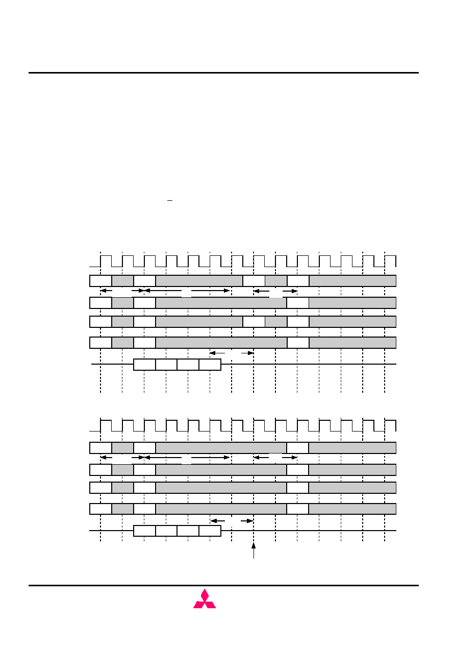
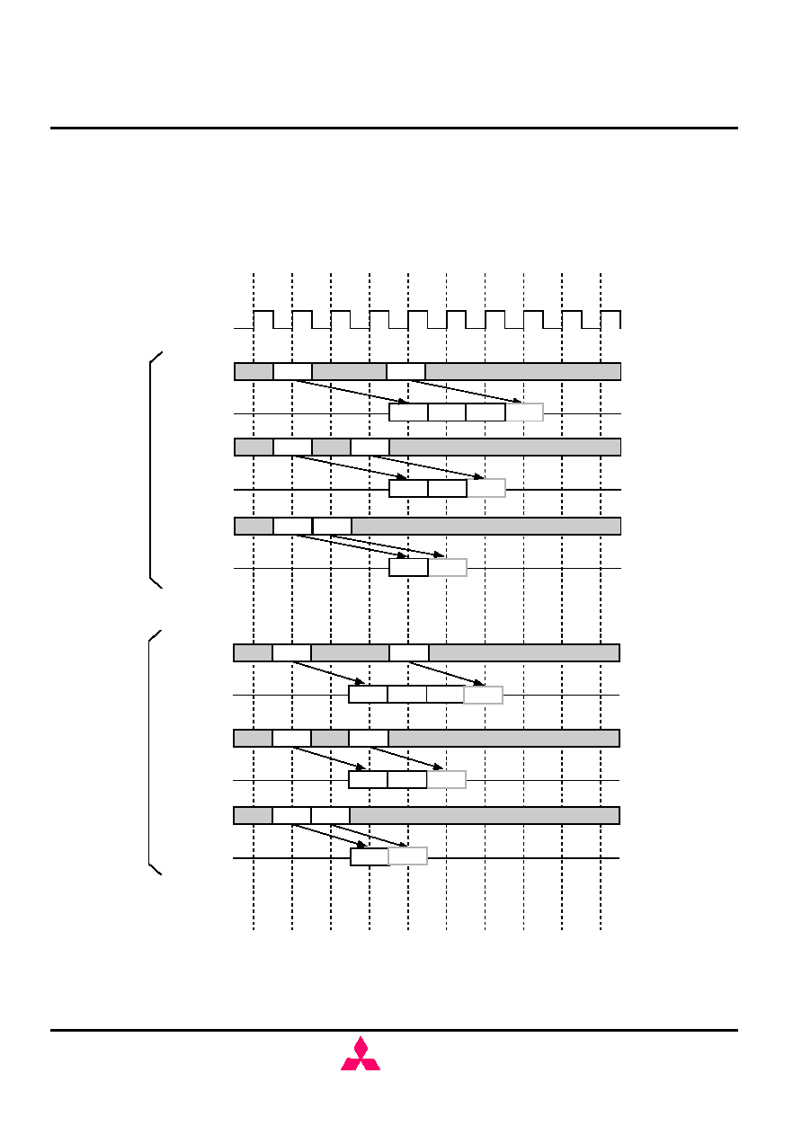
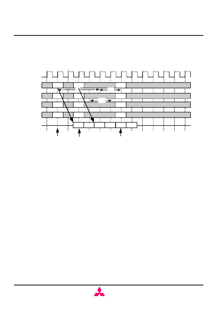
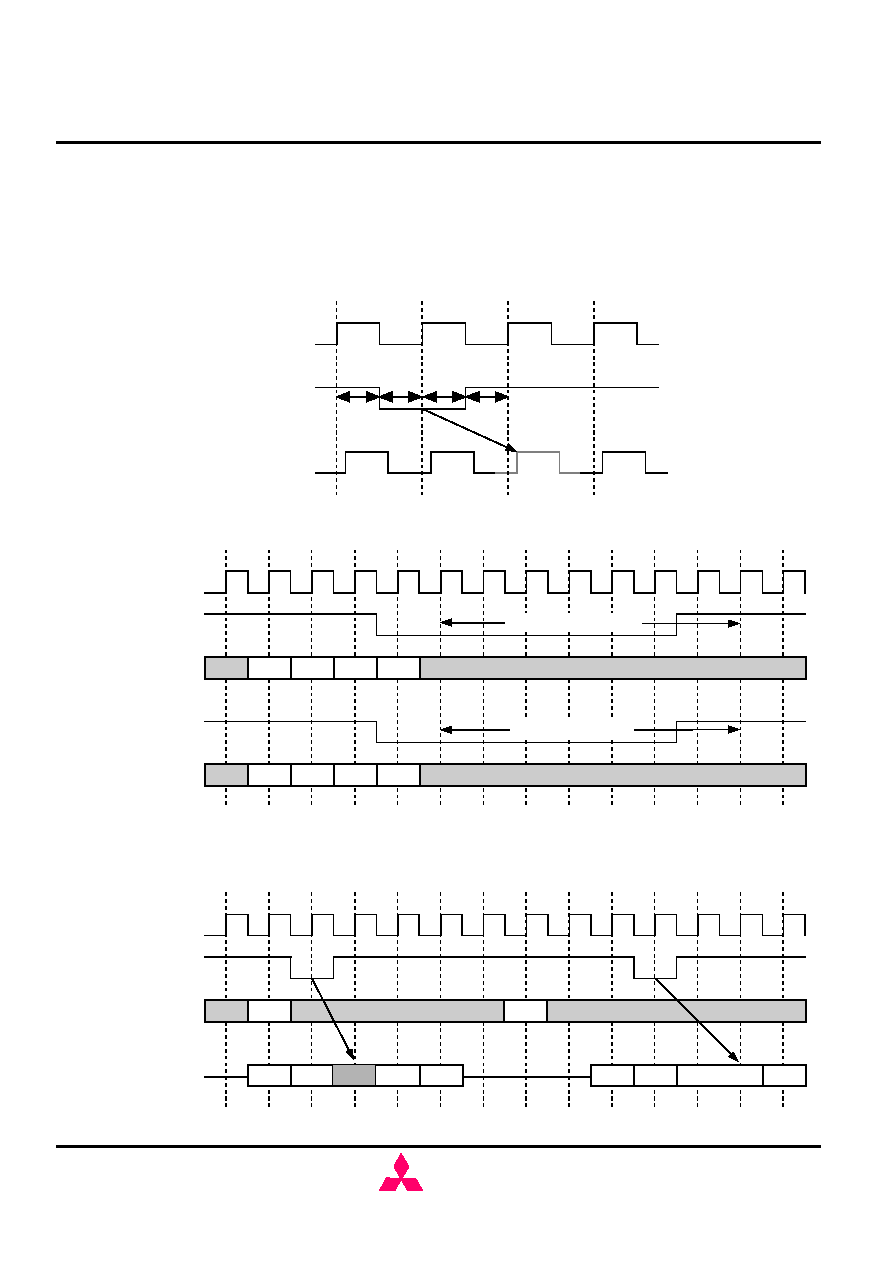
BURST INTERRUPTION
[ Read Interrupted by Read ]
Burst read oparation can be interrupted by new read of the same or the other bank. Random
column access is allowed READ to READ interval is minimum 1 CK
Read Interrupted by Read (BL=4, CL=2)
CK
Command
A10
DQ
READ
Y a
0
00
READ
Y b
0
00
Qa0
Qa2
Qb0
Qc0
Qa1
Qc1
Qc2
READ
Y c
0
10
Qc3
[ Read Interrupted by Write ]
Burst read operation can be interrupted by write of any active bank. Random column access
is allowed. In this case, the DQ should be controlled adequately by us ing the DQMB0-7 to
prevent the bus contention. The output is disabled automatically 1 cycle after WRITE
assertion.
Read Interrupted by Write (BL=4, CL=2)
CK
Command
A10
DQ
READ
Y a
0
00
Qa0
Write
Y a
0
00
Da0
Da1
Da2
Da3
DQMB0-7
20
A0-9,11
BA0,1
A0-9,11
BA0,1
ACT
Xa
Xa
00
Output disable by DQM by WRITE
MH8S64AQFC -6,-6L,-7,-7L,-8,-8L
536,870,912-BIT (8,388,608 - WORD BY 64-BIT)SynchronousDRAM
MITSUBISHI LSIs
( / 55 )
22.Sep.2000
MIT-DS-0374-0.3
MITSUBISHI
ELECTRIC
Preliminary Spec.
Some contents are subject to change without notice.
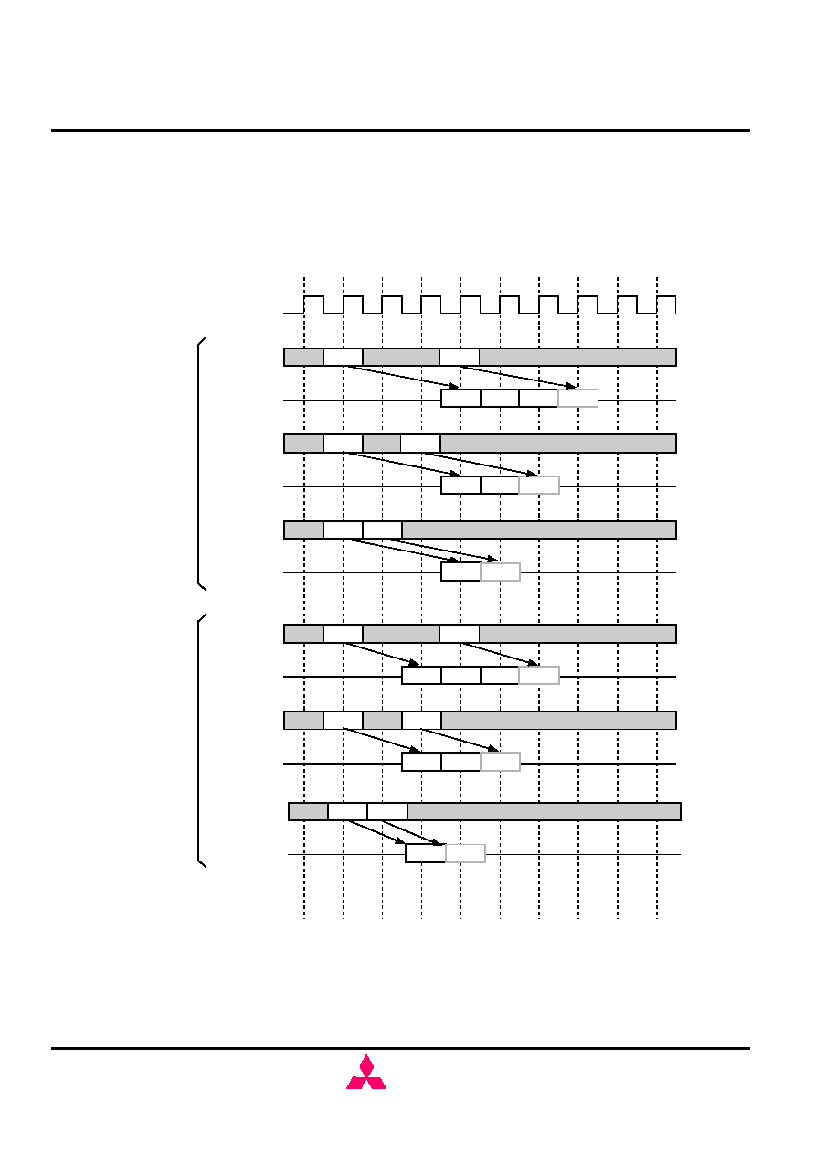
[ Read Interrupted by Precharge ]
A burst read operation can be interrupted by precharge of the same bank . Read to PRE
interval is minimum 1 CK. A PRE command output disable latency is equivalent to the
/CAS Latency.
Read Interrupted by Precharge (BL=4)
CK
Command
DQ
READ
PRE
Q0
Q1
Command
DQ
READ
PRE
Q0
Q1
Command
DQ
READ
PRE
Q0
Q2
Q1
Command
DQ
READ
PRE
Q0
CL=3
CL=2
21
Command
DQ
READ PRE
Command
DQ
READ PRE
Q0
Q2
Q0
Q1
MH8S64AQFC -6,-6L,-7,-7L,-8,-8L
536,870,912-BIT (8,388,608 - WORD BY 64-BIT)SynchronousDRAM
MITSUBISHI LSIs
( / 55 )
22.Sep.2000
MIT-DS-0374-0.3
MITSUBISHI
ELECTRIC
Preliminary Spec.
Some contents are subject to change without notice.
22
[ Read Interrupted by Burst Terminate ]
Similarly to the precharge, burst terminate command can interrupt burst read operation
and disable the data output. The term inated bank remains active,READ to TBST interval is
minimum of 1 CK. A TBSTcommand to output disable latency is equivalent to the /CAS
Latency.
Read Interrupted by Terminate (BL=4)
CK
Command
DQ
READ
TBST
Q0
Q1
Q2
CL=3
Command
DQ
READ
TBST
Q0
Q1
Command
DQ
READ TBST
Q0
Command
DQ
READ
TBST
Q0
Q1
Q2
CL=2
Command
DQ
READ
TBST
Q0
Q1
Command
DQ
READ TBST
Q0
MH8S64AQFC -6,-6L,-7,-7L,-8,-8L
536,870,912-BIT (8,388,608 - WORD BY 64-BIT)SynchronousDRAM
MITSUBISHI LSIs
( / 55 )
22.Sep.2000
MIT-DS-0374-0.3
MITSUBISHI
ELECTRIC
Preliminary Spec.
Some contents are subject to change without notice.
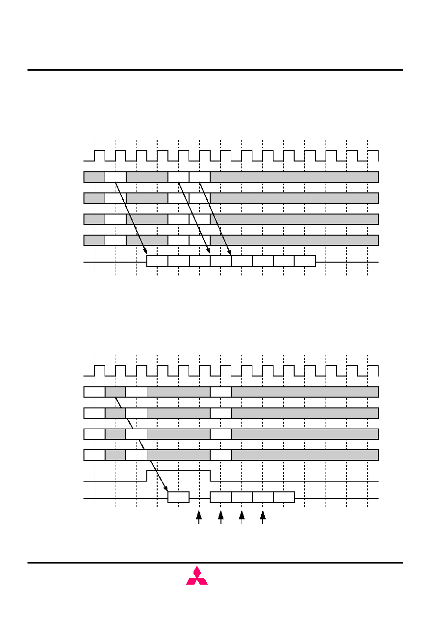
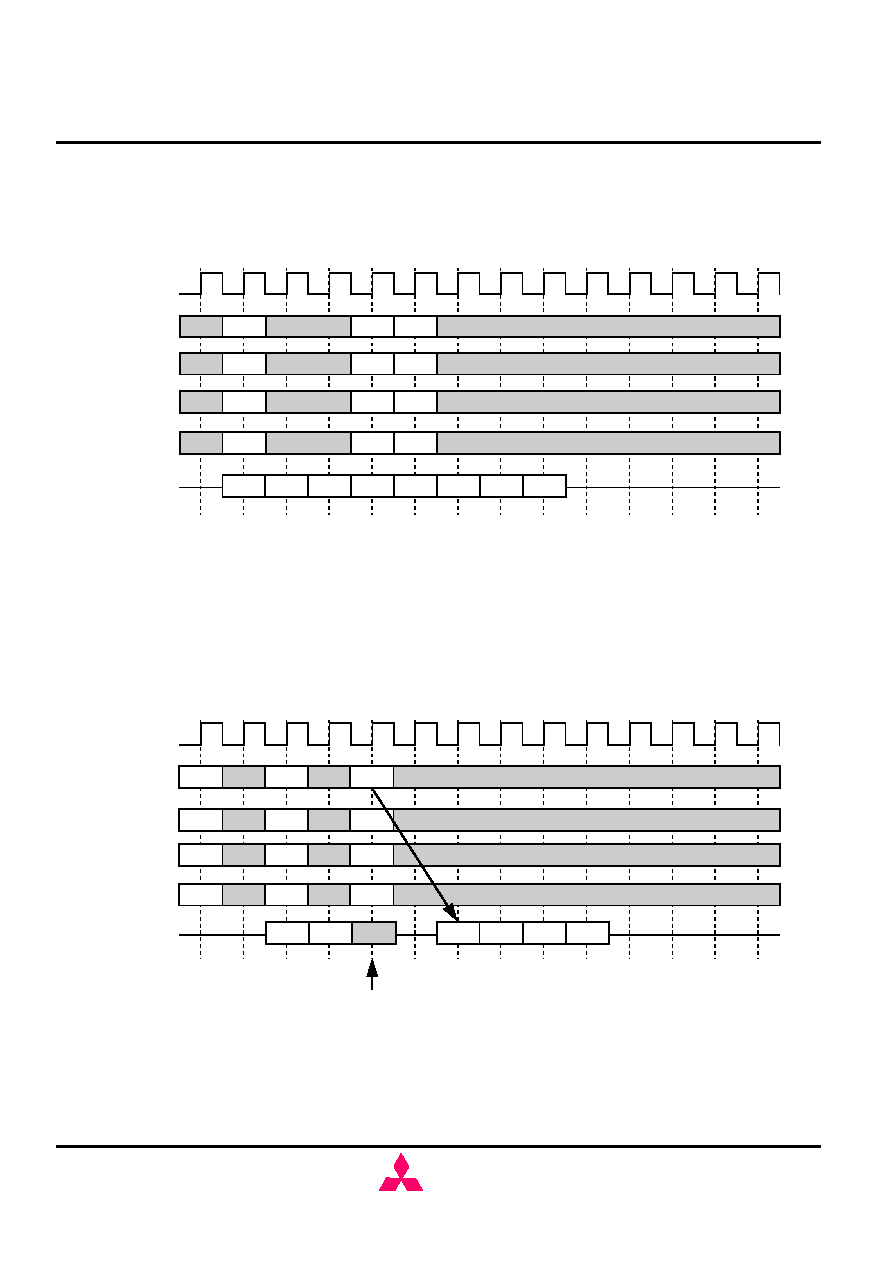
[ Write Interrupted by Write ]
Burst write operation can be interrupted by new write of any active bank. Random
column access is allowed. WRITE to WRITE interval is minimum 1 CK.
Write Interrupted by Write (BL=4)
CK
Command
A10
DQ
Write
Y a
0
00
Write
Y b
0
00
Da0
Da1
Da2
Db0
Dc0
Dc1
Write
Y c
0
10
Dc2
Dc3
[ Write Interrupted by Read ]
Burst write operation can be interrupted by read of any active bank. Random column
access is allowed. WRITE to READ interval is minimum 1 CK. The input data on DQ
at the interrupting READ cycle is "don't care".
Write Interrupted by Read (BL=4, CL=2)
CK
Command
A10
DQ
Write
Y a
0
00
Qb0
READ
Y b
0
00
Qb1
Da0
Qb2
Qb3
23
A0-9, 11
BA0,1
A0-9,11
BA0,1
ACT
Xa
Xa
00
Da1
don't care
MH8S64AQFC -6,-6L,-7,-7L,-8,-8L
536,870,912-BIT (8,388,608 - WORD BY 64-BIT)SynchronousDRAM
MITSUBISHI LSIs
( / 55 )
22.Sep.2000
MIT-DS-0374-0.3
MITSUBISHI
ELECTRIC
Preliminary Spec.
Some contents are subject to change without notice.
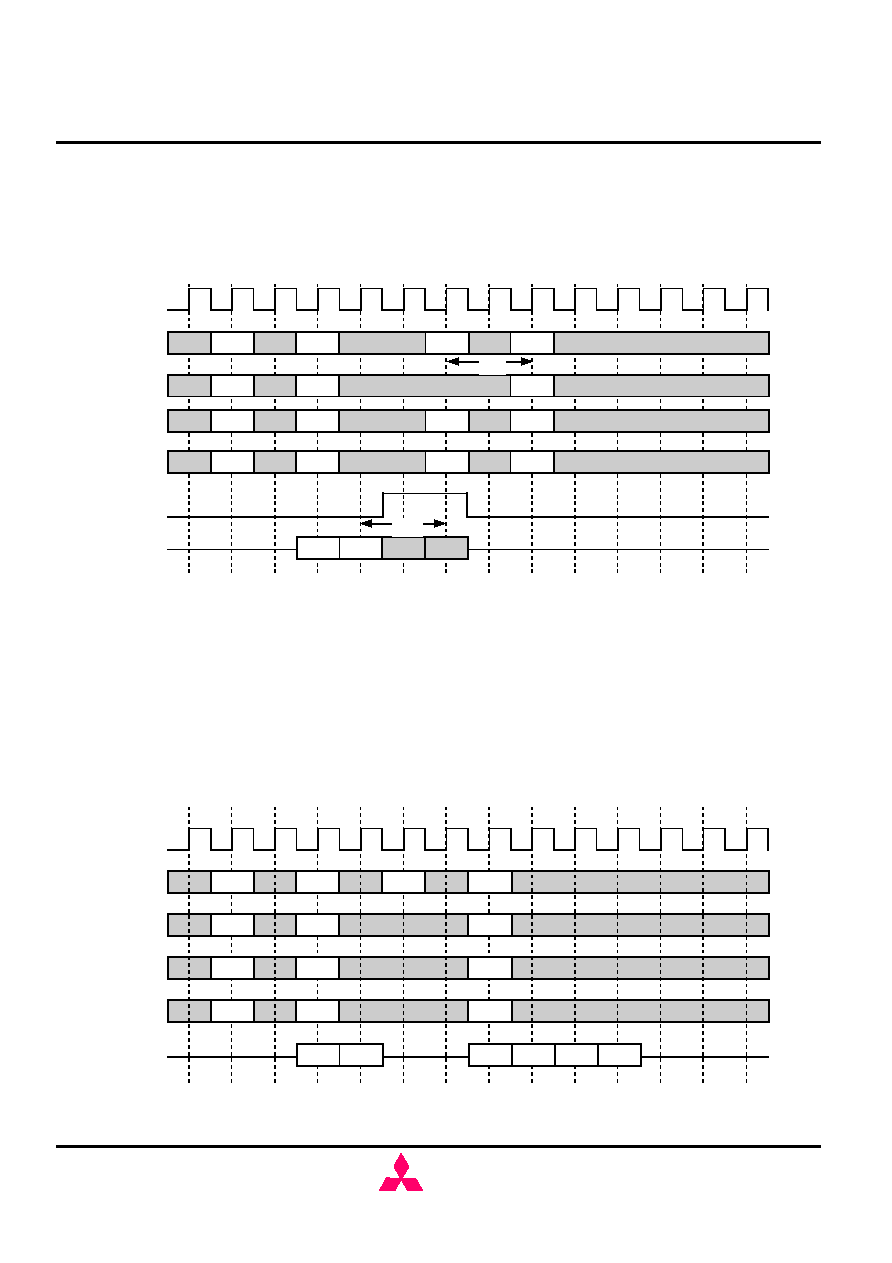
[ Write Interrupted by Precharge ]
Burst write operation can be interrupted by precharge of the same bank . Write
recovery time(tWR) is required from the last data to PRE command. During write
recovery, data inputs must be masked by DQM.
Write Interrupted by Precharge (BL=4)
CK
Command
A10
DQ
ACT
Xa
0
00
Write
0
00
Da0
Da1
DQMB0-7
ACT
Xa
0
00
tRP
[ Write Interrupted by Burst Terminate ]
Burst terminate command can terminate burst write operation. In this case, the
write recovery time is not required and the bank remains active.The WRITE to TBST
minimum interval is 1CK.
Write Interrupted by Burst Terminate (BL=4)
CK
Command
A10
DQ
ACT
Xa
0
00
TBST
Da0
Da1
24
A0-9,11
BA0,1
A0-9,11
BA0,1
Y a
PRE
0
00
tWR
Write
Y a
0
00
Write
Y b
0
00
Db0
Db1
Db2
Db3
MH8S64AQFC -6,-6L,-7,-7L,-8,-8L
536,870,912-BIT (8,388,608 - WORD BY 64-BIT)SynchronousDRAM
MITSUBISHI LSIs
( / 55 )
22.Sep.2000
MIT-DS-0374-0.3
MITSUBISHI
ELECTRIC
Preliminary Spec.
Some contents are subject to change without notice.
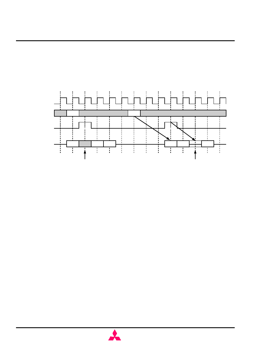
[ Write with Auto-Precharge interrupted by Write or Read to anotehr Bank ]
Burst write with auto-precharge can be interrupted by write or read toanother bank .
Next ACT command can be issued after (BL+tWR-1+tRP) from the WRITEA. Auto-
precharge interrrupted by a command to the same bank is inhibited.
WRITEA Interrupted by WRITE to another bank (BL=4)
CK
Command
A10
DQ
Write
Y a
1
00
Write
0
10
Da0
Da1
ACT
Xa
Xa
00
tRP
WRITEA interrupted by READ to another bank (CL=2,BL=4)
CK
Command
A10
DQ
Write
Y a
1
00
Da0
Da1
25
A0-9,11
BA0,1
A0-9,11
BA0,1
Y a
Read
Y b
0
10
ACT
Xa
Xa
00
Db0
Db1
Db2
Db3
Db0
Db1
Db2
Db3
auto-precharge interrupted
activate
BL
tWR
tRP
BL
tWR
auto-precharge interrupted
activate
MH8S64AQFC -6,-6L,-7,-7L,-8,-8L
536,870,912-BIT (8,388,608 - WORD BY 64-BIT)SynchronousDRAM
MITSUBISHI LSIs
( / 55 )
22.Sep.2000
MIT-DS-0374-0.3
MITSUBISHI
ELECTRIC
Preliminary Spec.
Some contents are subject to change without notice.
[ Read with Auto-Precharge interrupted by Read to anotehr Bank ]
Burst read with auto-precharge can be interrupted by read toanother bank . Next
ACT command can be issued after (BL+tRP) from the READA. Auto-precharge
interrrupted by a command to the same bank is inhibited.
READA Interrupted by READ to another bank (CL=2,BL=4)
CK
Command
A10
DQ
Read
Y a
1
00
Read
0
10
Qa0
Qa1
ACT
Xa
Xa
00
tRP
26
A0-9,11
BA0,1
Y a
Qb0
Qb1
Qb2
Qb3
auto-precharge interrupted
activate
BL
tWR
Full Page Burst
Full page burst length is available for only the sequential burst type. Full page burst
read or write is repeated untill aPrecharge or a Burst Terminate command is
issued. In case of the full page burst , a read or write with auto-precharge command
is illegal.
Single Write
When single write mode is set, burst length for write is always one, independently
of Burst Length defined by (A2-0).
MH8S64AQFC -6,-6L,-7,-7L,-8,-8L
536,870,912-BIT (8,388,608 - WORD BY 64-BIT)SynchronousDRAM
MITSUBISHI LSIs
( / 55 )
22.Sep.2000
MIT-DS-0374-0.3
MITSUBISHI
ELECTRIC
Preliminary Spec.
Some contents are subject to change without notice.
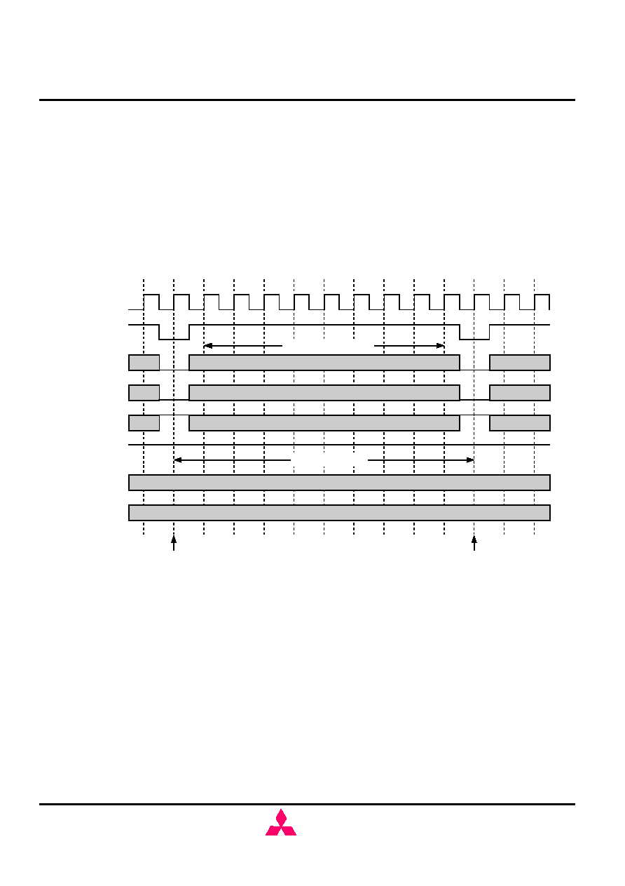
AUTO REFRESH
Single cycle of auto-refresh is initiated with a REFA(/CS=/RAS=/CAS=L,
/WE=/CKE=H) command. The refresh address is generated internally. 4096 REFA
cycle within 64m s refresh 128Mbit memory cells. The auto-refresh is performed on
4banks concurrently. Before performing an auto-refresh, all banks must be in the
idle state. Auto-refresh to auto-refresh interval is minimum tRFC. Any command
must not be issued before tRFC from the REFA command.
Auto-Refresh
CK
/S
/RAS
/CAS
/WE
CKE
A0-11
BA0,1
Auto Refresh on All Banks
Auto Refresh on All Banks
minimum tRFC
NOP or DESLECT
27
MH8S64AQFC -6,-6L,-7,-7L,-8,-8L
536,870,912-BIT (8,388,608 - WORD BY 64-BIT)SynchronousDRAM
MITSUBISHI LSIs
( / 55 )
22.Sep.2000
MIT-DS-0374-0.3
MITSUBISHI
ELECTRIC
Preliminary Spec.
Some contents are subject to change without notice.
SELF REFRESH
Self-refresh mode is entered by issuing a REFS command (/CS=/RAS=/CAS=L,
/WE=H, CKE=L). Once the self-refresh is initiated, it is maintained as log as CKE is
kept low.During the self-refresh mode, CKE is asynchronous and the only enabled
input , all other inputs including CK are disabled and ignored, so that power
consumption due to synchronous inputs is saved. To exit the self-refresh, supplying
stable CK inputs , asserting DESEL or NOP command and then asserting CKE=H.
After tRFC from the 1s t CK edge follwing CKE=H, all banks are in the idle state and
a new command can be issued after, but DESEL or NOP commands must be
asserted till then.
Self-Refresh
CK
/S
/RAS
/CAS
/WE
CKE
A0-11
BA0,1
Self Refresh Entry
Self Refresh Exit
X
00
minimum tRFC
for recovery
Stable CK
NOP
new command
28
MH8S64AQFC -6,-6L,-7,-7L,-8,-8L
536,870,912-BIT (8,388,608 - WORD BY 64-BIT)SynchronousDRAM
MITSUBISHI LSIs
( / 55 )
22.Sep.2000
MIT-DS-0374-0.3
MITSUBISHI
ELECTRIC
Preliminary Spec.
Some contents are subject to change without notice.
CLK SUSPEND and POWER DOWN
CKE controls the internal CLK at the following cycle. Figure below shows how CKE
works. By negating CKE, the next internal CLK is suspended. The purpose of CLK
suspend is power down, output suspend or input suspend. CKE is a synchronous
input except during the self-refresh mode. CLK suspend can be performed either
when the banks are active or idle. A command at the suspended cycle is ignored.
CK
(ext.CLK)
CKE
int.CLK
Power Down by CKE
CK
Command
PRE
CKE
Command
CKE
ACT
NOP
NOP
NOP
NOP
Standby Power Down
Activ e Power Down
NOP
NOP
DQ Suspend by CKE
CK
Command
DQ
Write
D0
D1
D2
D3
CKE
READ
Q0
Q1
Q2
Q3
29
tIH
tIS
tIH
tIS
MH8S64AQFC -6,-6L,-7,-7L,-8,-8L
536,870,912-BIT (8,388,608 - WORD BY 64-BIT)SynchronousDRAM
MITSUBISHI LSIs
( / 55 )
22.Sep.2000
MIT-DS-0374-0.3
MITSUBISHI
ELECTRIC
Preliminary Spec.
Some contents are subject to change without notice.
DQM CONTROL
DQMB0-7 is a dual function signal defined as the data mask for writes and the
output disable for reads. During writes, DQMB0-7 masks input data word by word.
DQMB0-7 to Data In latency is 0.
During reads, DQMB0-7 forces output to Hi-Z word by word. DQMB0-7 to output Hi-Z
latency is 2.
DQM Function
CK
Command
DQ
Write
D0
D2
D3
DQMB0-7
READ
Q0
Q1
Q3
masked by DQMB=H
disabled by DQMB=H
30
MH8S64AQFC -6,-6L,-7,-7L,-8,-8L
536,870,912-BIT (8,388,608 - WORD BY 64-BIT)SynchronousDRAM
MITSUBISHI LSIs
( / 55 )
22.Sep.2000
MIT-DS-0374-0.3
MITSUBISHI
ELECTRIC
Preliminary Spec.
Some contents are subject to change without notice.
ABSOLUTE MAXIMUM RATINGS
Symbol
Parameter
Condition
Ratings
Unit
Vdd
VI
VO
IO
Pd
Topr
Tstg
Supply Voltage
Input Voltage
Output Voltage
Output Current
Power Dissipation
Operating Temperature
Storage Temperature
with respect to Vs s
with respect to Vs s
with respect to Vs s
Ta=25∞C
-0.5 ~ 4.6
50
4
0 ~ 70
-40 ~ 100
V
V
V
mA
W
∞C
∞C
RECOMMENDED OPERATING CONDITION
(Ta=0 ~ 70∞C, unless otherwise noted)
Symbol
Vdd
Vss
VIH
VIL
Parameter
Supply Voltage
High-Level Input Voltage all inputs
Supply Voltage
Low-Level Input Voltage all inputs
Limits
Unit
Min.
Typ.
Max.
3.0
0
2.0
-0.3
3.3
0
3.6
0
Vdd+0.3
0.8
V
V
V
V
CAPACITANCE
(Ta=0 ~ 70∞C, Vdd = 3.3 ± 0.3V, Vss = 0V, unless otherwise noted)
Symbol
CI(A)
CI(C)
CI(K)
CI/O
Parameter
Input Capacitance, address pin
Input Capacitance, /RAS,/CAS,/WE
Input Capacitance, CK pin
Input Capacitance, I/O pin
Tes t Condition
Limits(max.)
35
35
35
22
31
Unit
pF
pF
pF
pF
@1MHz
1.4V bias
200mV swing
Note)
1:VIH(max)=5.5V f or pulse width less than 10ns.
2.VIL(min)=-1.0 f or pulse width less than 10ns.
-0.5 ~ 4.6
-0.5 ~ 4.6
MH8S64AQFC -6,-6L,-7,-7L,-8,-8L
536,870,912-BIT (8,388,608 - WORD BY 64-BIT)SynchronousDRAM
MITSUBISHI LSIs
( / 55 )
22.Sep.2000
MIT-DS-0374-0.3
MITSUBISHI
ELECTRIC
Preliminary Spec.
Some contents are subject to change without notice.
AVERAGE SUPPLY CURRENT from Vdd
(Ta=0 ~70∞C, Vdd = 3.3 ± 0.3V, Vss = 0V, unless otherwise noted)
AC OPERATING CONDITIONS AND CHARACTERISTICS
(Ta=0 ~ 70∞C, Vdd = 3.3 ± 0.3V, Vss = 0V, unless otherwise noted)
32
Symbol
Parameter
Test Condition
Limits
Unit
Min. Max.
VOH(DC) High-Level Output Voltage(DC) IOH=-2mA
2.4
V
VOL(DC) Low-Level Output Voltage(DC) IOL=2mA
0.4
V
VOH(AC) High-Level Output Voltage(AC) CL=50pF, IOH=-
2mA
2
V
VOL(AC) Low-Level Output Voltage(AC) CL=50pF, IOL=2mA
0.8
V
IOZ
Off-stare Output Current
Q floating VO=0 ~ Vdd
-10
10
uA
Ii
Input Current
VIH=0 ~ Vdd+0.3V
-40
40
uA
Note)
1:Icc(max) is specif ied at the output open condition.
2.Input signals are changed one time during 30ns.
480
8
4
100
520
640
8
60
120
80
Test Condition
Unit
tRC=min.tCLK=min, BL=1,CL=3
mA
CKE=L,tCLK=15ns, /CS>Vcc-0.2V
mA
CKE=CLK=L, /CS>Vcc-0.2V
mA
mA
tCLK=min, BL=4, CL=3,all banks activ e(discerte)
mA
tRC=min, tCLK=min
mA
CKE <0.2V
mA
CKE=H,tCLK=15ns,VIH>Vcc-0.2V,VIL<0.2V
Symbol
Icc1
Icc2P
Icc2PS
Icc2NS
Icc4
Icc5
Icc6
Icc2N
Parameter
operating current
one bank activ e (discrete)
precharge stanby
current
in power-down mode
burst current
auto-refresh current
self-refresh current
CKE=H,CLK=L,VIH>Vcc-0.2V,VIL<0.2V(f ixed)
mA
precharge stanby current
in non power-down mode
mA
CKE=H,tCLK=15ns
Icc3NS
Icc3N
CKE=H,CLK=L
mA
active stanby current
in non power-down mode
one bank activ e (discrete)
3.2
-6,-7,-8
-6L,-7L,-8L
520
8
4
100
640
640
8
60
120
80
Limits
(max)
3.2
-7,-7L
-6,-6L
-8,-8L
MH8S64AQFC -6,-6L,-7,-7L,-8,-8L
536,870,912-BIT (8,388,608 - WORD BY 64-BIT)SynchronousDRAM
MITSUBISHI LSIs
( / 55 )
22.Sep.2000
MIT-DS-0374-0.3
MITSUBISHI
ELECTRIC
Preliminary Spec.
Some contents are subject to change without notice.
AC TIMING REQUIREMENTS (SDRAM Component)
(Ta=0 ~ 70∞C, Vdd = 3.3 ± 0.3V, Vss = 0V, unless otherwise noted)
Input Pulse Levels: 0.8V to 2.0V
Input Timing Measurement Level: 1.4V
CK
Signal
1.4V
1.4V
Any AC timing is
referenced to the input
signal crossing
through 1.4V.
33
Limits
Symbol Parameter
-7,-7L
Unit
Min.
Max.
tCLK
CK cycle time
ns
tCH
CK High pulse width
3
10
ns
tCL
CK Low pilse width
3
ns
tT
Transition time of CK
1
10
ns
tIS
Input Setup time(all inputs)
2
ns
tIH
Input Hold time(all inputs)
1
ns
tRC
Row cycle tim e
70
ns
tRCD Row to Column Delay
20
ns
tRAS
Row Active time
50
100K
ns
tRP
Row Precharge tim e
20
ns
tWR
Write Recovery time
12
ns
tRRD Act to Act Deley time
20
ns
tRSC Mode Register Set Cycle time
10
ns
tSRX Self Refresh Exit tim e
10
ns
tREF
Refresh Interval time
64
ms
-8,-8L
Min.
Max.
3
13
3
1
10
2
1
70
20
50
100K
20
12
20
10
10
64
CL=2
CL=3
10
10
ns
tPDE Power Down Exit time
10
ns
10
-6,-6L
Min.
Max.
2.5
7.5
1
10
1.5
0.8
67.5
20
45
100K
20
12
15
10
7.5
64
10
7.5
2.5
MH8S64AQFC -6,-6L,-7,-7L,-8,-8L
536,870,912-BIT (8,388,608 - WORD BY 64-BIT)SynchronousDRAM
MITSUBISHI LSIs
( / 55 )
22.Sep.2000
MIT-DS-0374-0.3
MITSUBISHI
ELECTRIC
Preliminary Spec.
Some contents are subject to change without notice.
1.4V
1.4V
DQ
CK
tAC
tOH
tOHZ
SWITCHING CHARACTERISTICS (SDRAM Component)
(Ta=0 ~ 70∞C, Vdd = 3.3 ± 0.3V, Vss = 0V, unless otherwise note3)
Output Load Condition
DQ
CK
Output Timing
Measurement
Reference Point
1.4V
1.4V
34
Note)
1 If clock rising time is longer than 1ns,(tT/2-0.5)ns should be added to parameter.
Limits
Symbol Parameter
-8
Unit
Min.
Max.
tAC
Access time from CK
7
ns
tOH
Output Hold tim e
3
ns
from CK
tOLZ
Delay time, output low
impedance from CK
0
ns
tOHZ
Delay time, output high
impedance from CK
3
ns
6
-7
Min.
6
3
0
3
6
Max.
6
6
ns
CL=2
CL=3
CL=2
V
OUT
50pF
tOLZ
3
ns
3
CL=3
-6
Min.
6
3
0
2.7
5.4
Max.
5.4
2.7
MH8S64AQFC -6,-6L,-7,-7L,-8,-8L
536,870,912-BIT (8,388,608 - WORD BY 64-BIT)SynchronousDRAM
MITSUBISHI LSIs
( / 55 )
22.Sep.2000
MIT-DS-0374-0.3
MITSUBISHI
ELECTRIC
Preliminary Spec.
Some contents are subject to change without notice.
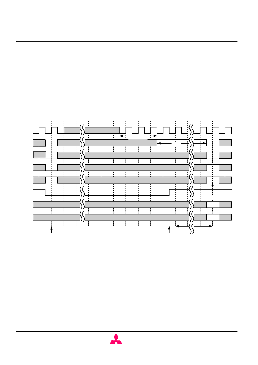
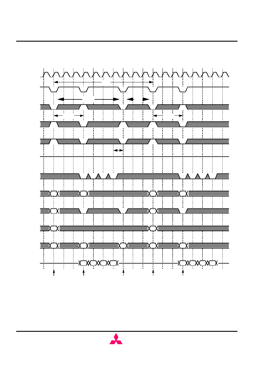
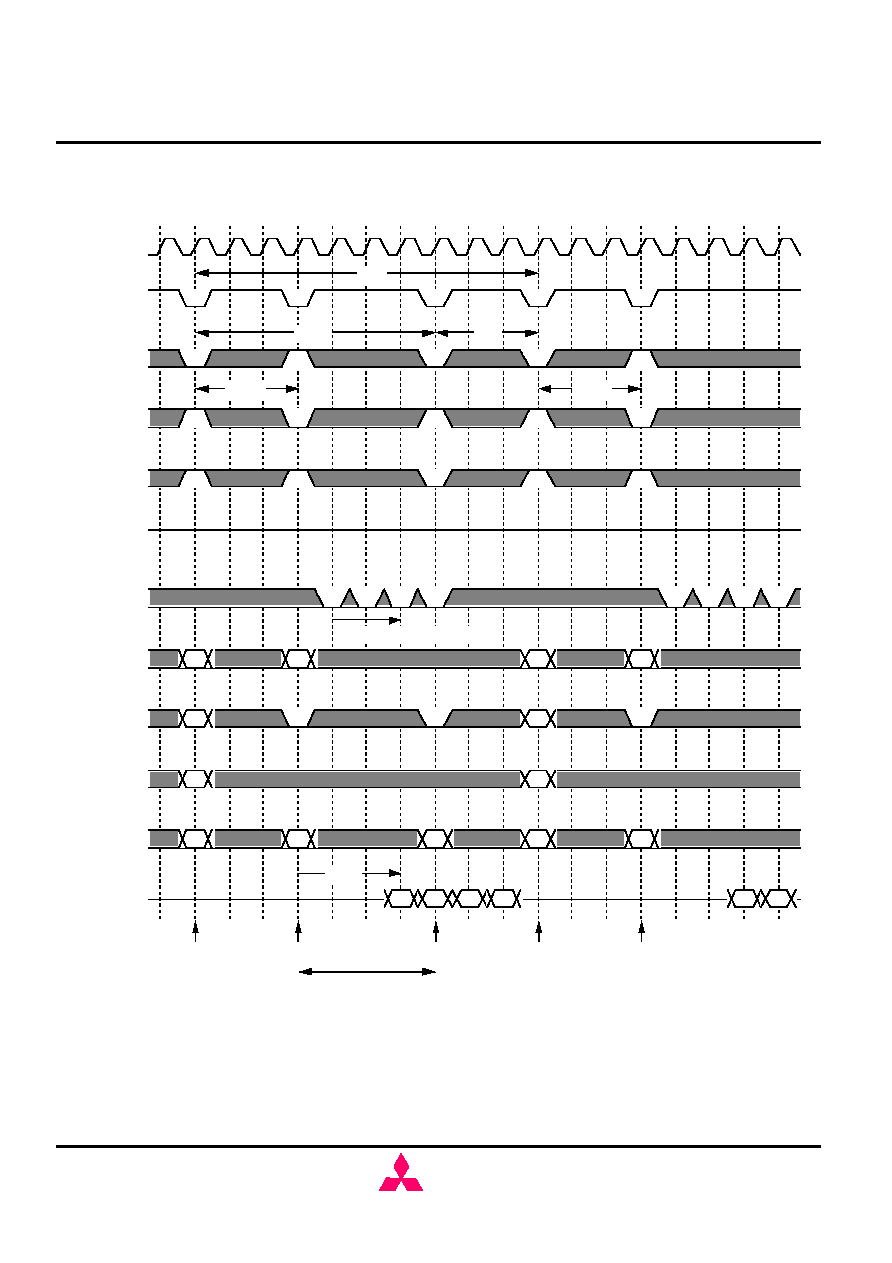
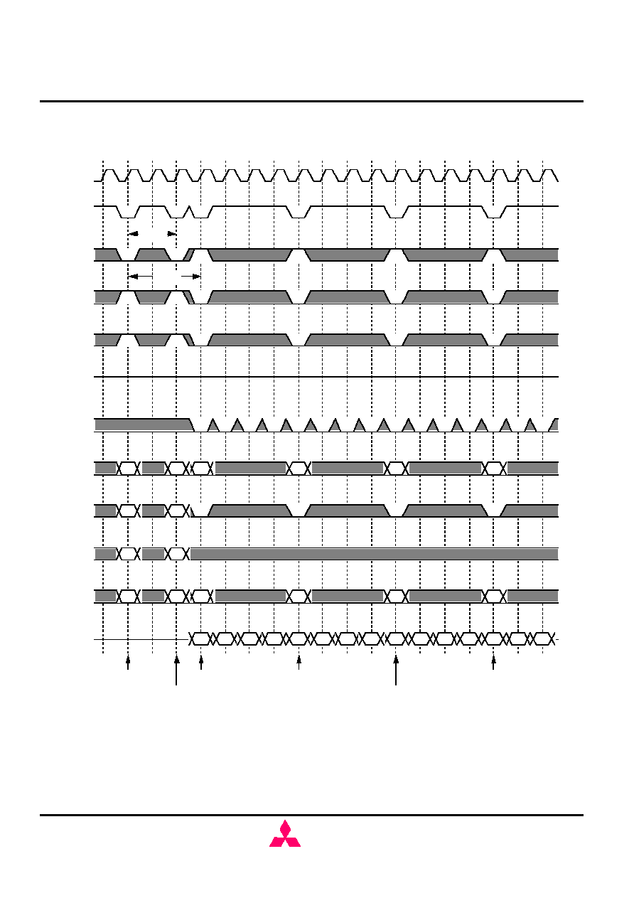
Burst Write (single bank) @BL=4
/CS
/RAS
/CAS
/WE
CKE
BA0,1
DQ
X
X
X
0
Y
0
0
D0
D0
D0
D0
X
X
X
0
Y
0
D0
D0
D0
D0
ACT#0
WRITE#0
PRE#0
ACT#0
WRITE#0
0
1
2
3
4
5
6
7
8
9
10
11
12
13
14
15
16
17
tRCD
tWR
tRP
tRC
tRCD
CLK
Italic parameter indicates minimum case
tRAS
A0-8
A10
DQM
A9,11
35
MH8S64AQFC -6,-6L,-7,-7L,-8,-8L
536,870,912-BIT (8,388,608 - WORD BY 64-BIT)SynchronousDRAM
MITSUBISHI LSIs
( / 55 )
22.Sep.2000
MIT-DS-0374-0.3
MITSUBISHI
ELECTRIC
Preliminary Spec.
Some contents are subject to change without notice.
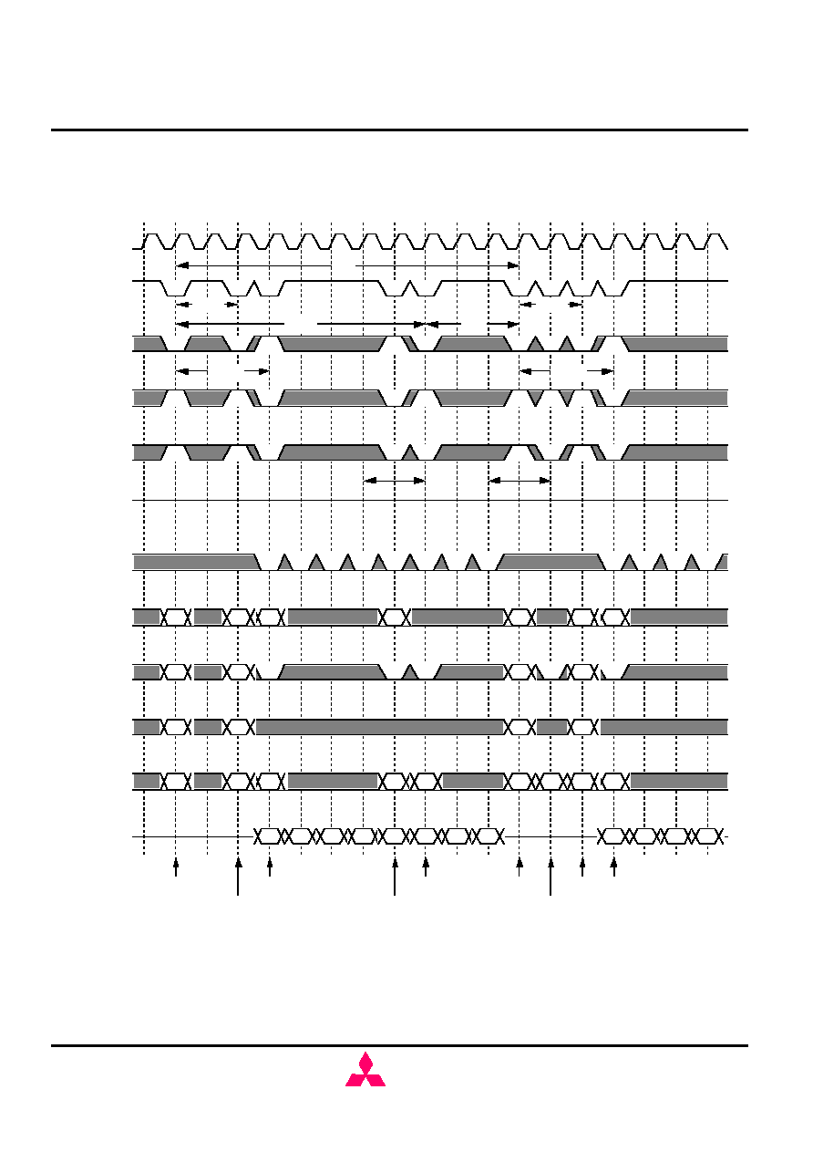
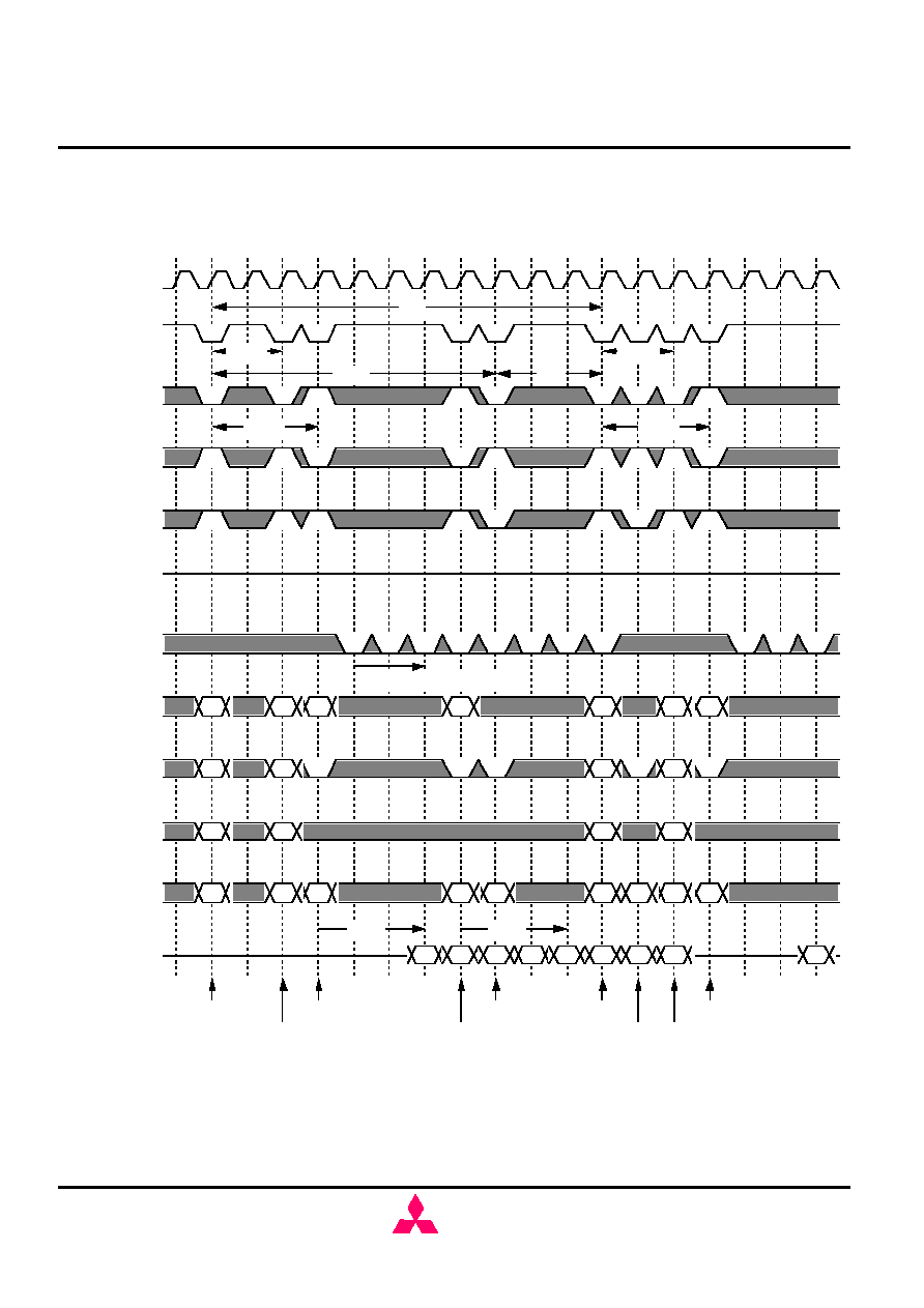
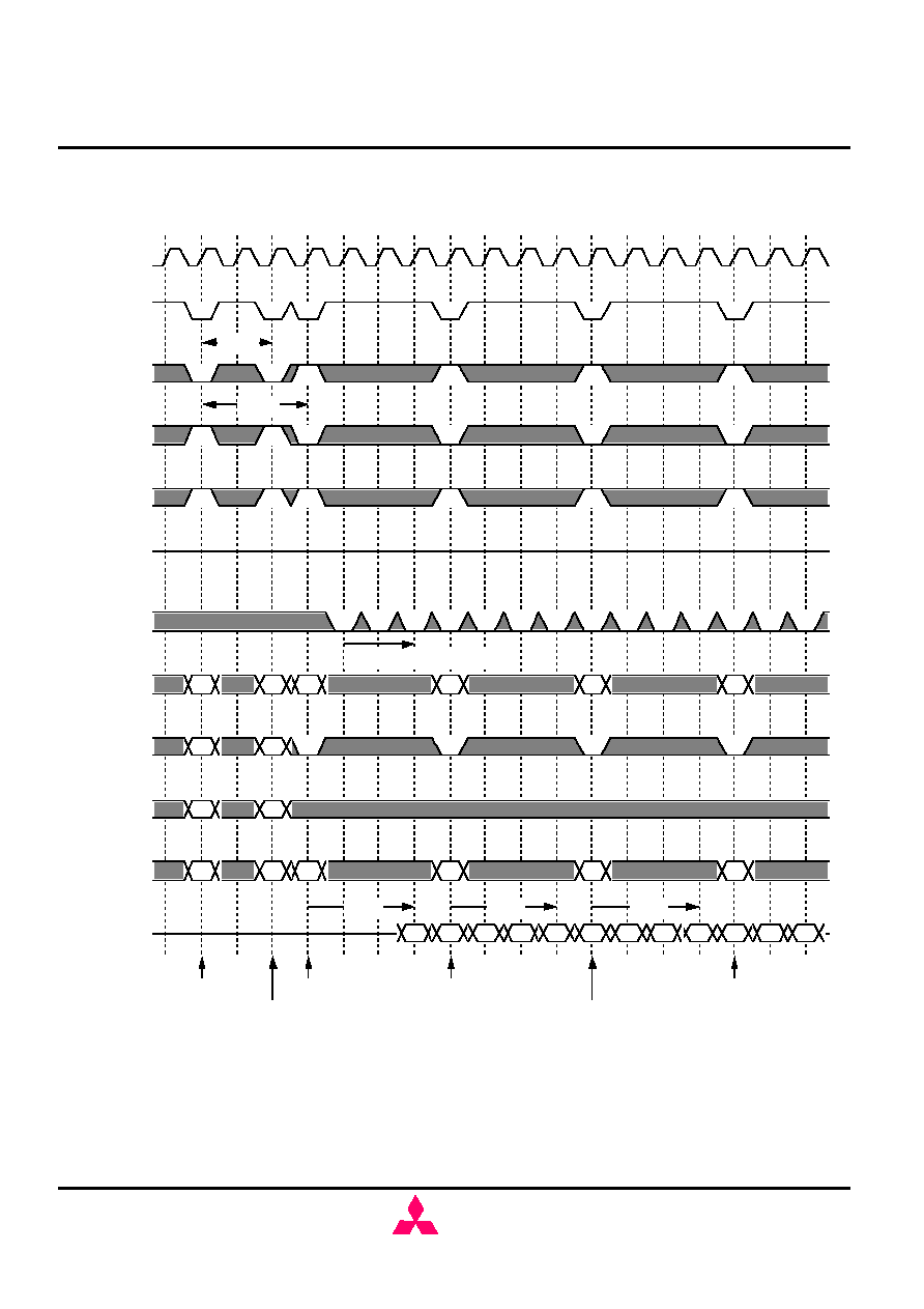
Burst Write (multi bank) @BL=4
/CS
/RAS
/CAS
/WE
CKE
BA0,1
DQ
X
X
X
0
Y
0
1
D0
D0
D0
D0
X
X
0
Y
0
D0
D0
D0
D0
ACT#0
WRITE#0
PRE#0
ACT#0
WRITE#0
0
1
2
3
4
5
6
7
8
9
10
11
12
13
14
15
16
17
tRCD
tRAS
tWR
tRP
tRC
tRCD
D1
D1
D1
D1
X
X
X
1
tRRD
Y
tWR
0
X
1
X
X
X
2
tRRD
ACT#1
WRITE#1
PRE#1
ACT#2
CLK
Italic parameter indicates minimum case
A0-8
A10
DQM
A9,11
36
MH8S64AQFC -6,-6L,-7,-7L,-8,-8L
536,870,912-BIT (8,388,608 - WORD BY 64-BIT)SynchronousDRAM
MITSUBISHI LSIs
( / 55 )
22.Sep.2000
MIT-DS-0374-0.3
MITSUBISHI
ELECTRIC
Preliminary Spec.
Some contents are subject to change without notice.
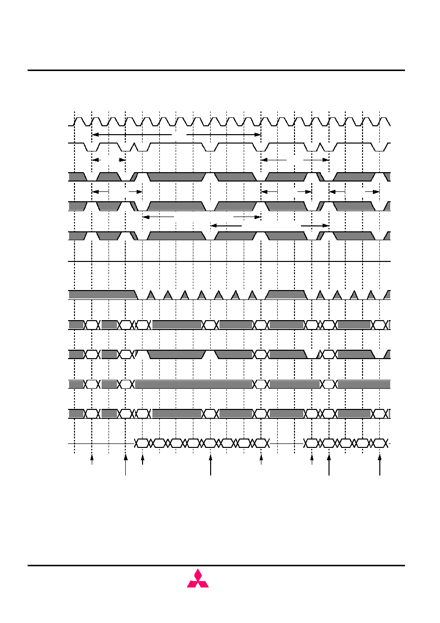
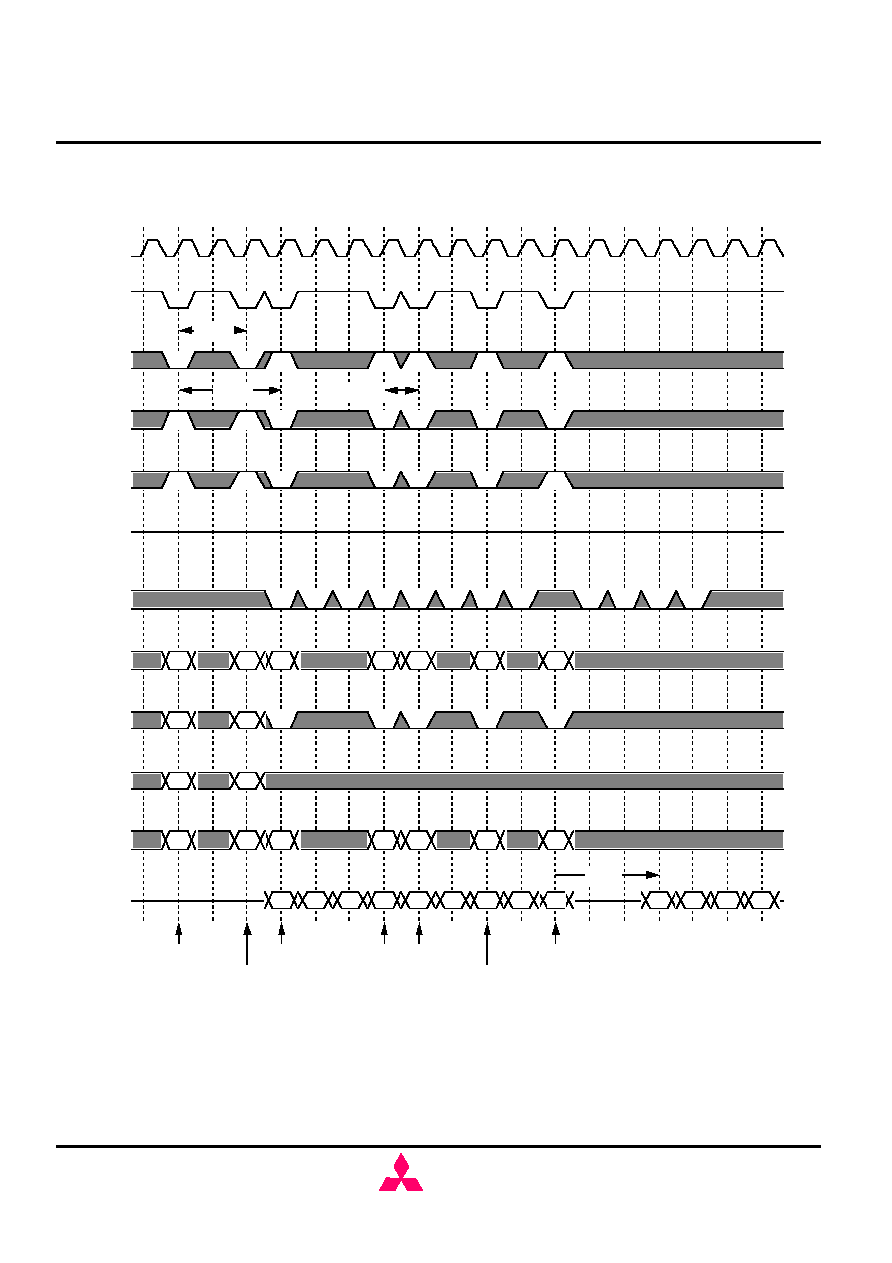
Burst Read (single bank) @BL=4 CL=3
/CS
/RAS
/CAS
/WE
CKE
BA0,1
DQ
X
X
X
0
Y
0
0
Q0
Q0
Q0
Q0
X
X
X
0
Y
0
Q0
Q0
ACT#0
READ#0
PRE#0
ACT#0
READ#0
0
1
2
3
4
5
6
7
8
9
10
11
12
13
14
15
16
17
tRCD
tRAS
tRP
tRC
tRCD
CL=3
READ to PRE
BL allows full data out
DQM read latency =2
CLK
Italic parameter indicates minimum case
A0-7
A10
DQM
A8,9,11
37
MH8S64AQFC -6,-6L,-7,-7L,-8,-8L
536,870,912-BIT (8,388,608 - WORD BY 64-BIT)SynchronousDRAM
MITSUBISHI LSIs
( / 55 )
22.Sep.2000
MIT-DS-0374-0.3
MITSUBISHI
ELECTRIC
Preliminary Spec.
Some contents are subject to change without notice.
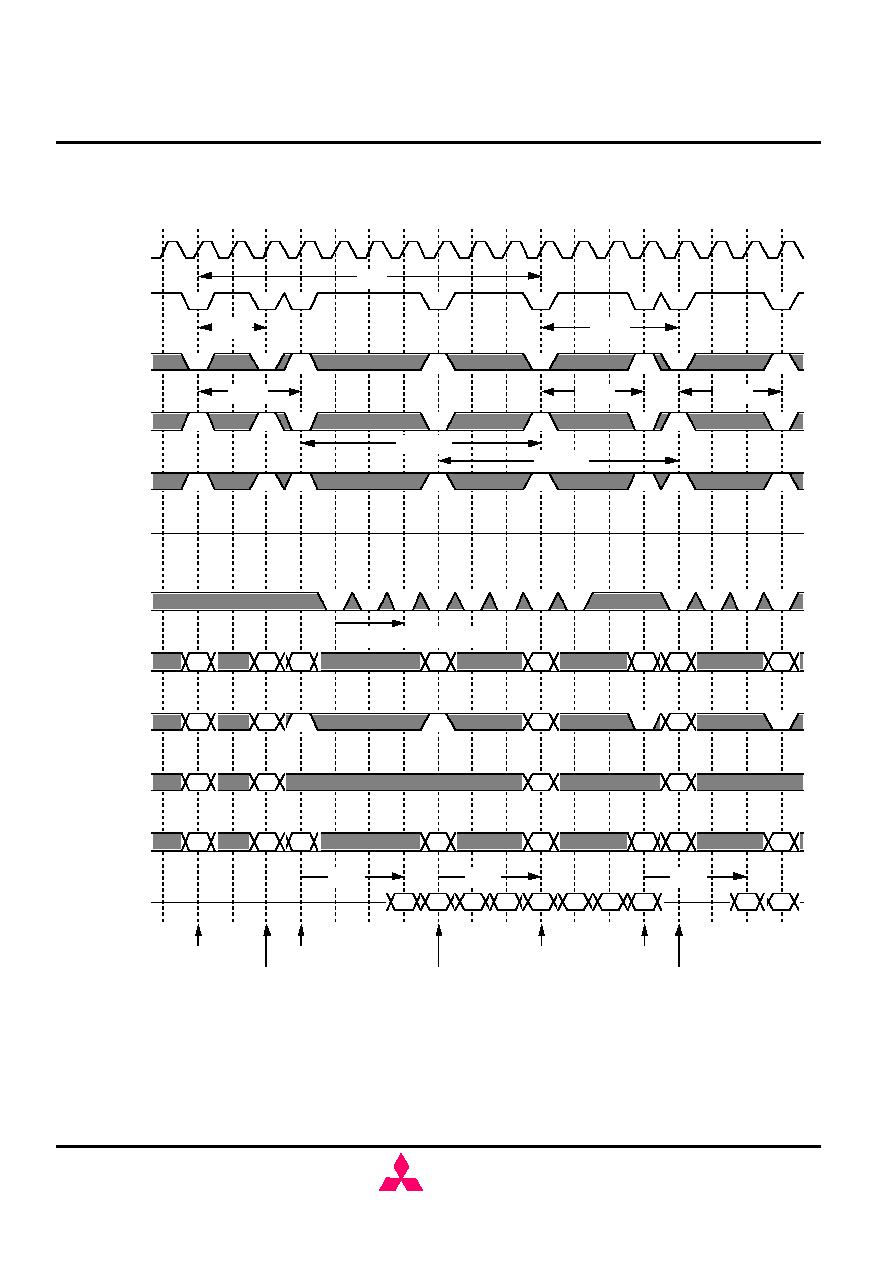
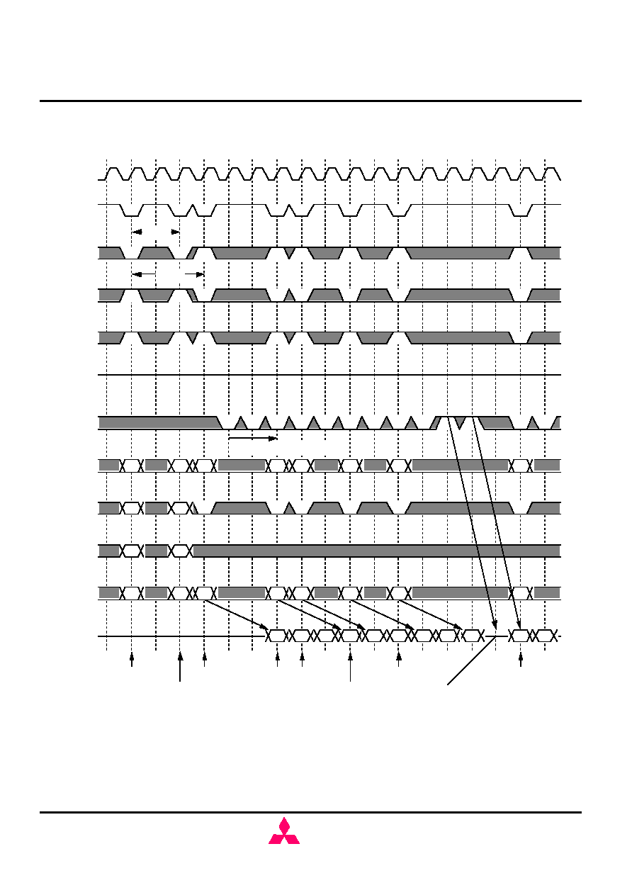
Burst Read (multiple bank) @BL=4 CL=3
/CS
/RAS
/CAS
/WE
CKE
BA0,1
DQ
X
X
X
0
Y
0
0
Q0
Q0
Q0
Q0
X
X
X
0
Y
0
Q0
ACT#0
READ#0
PRE#0
ACT#0
READ#0
0
1
2
3
4
5
6
7
8
9
10
11
12
13
14
15
16
17
tRCD
tRAS
tRP
tRC
tRCD
CL=3
DQM read latency =2
tRRD
X
X
X
1
ACT#1
Y
1
tRRD
Q1
Q1
Q1
Q1
X
X
X
2
1
CL=3
READ#1
PRE#1
ACT#2
CLK
Italic parameter indicates minimum case
A0-8
A10
DQM
A9,11
38
MH8S64AQFC -6,-6L,-7,-7L,-8,-8L
536,870,912-BIT (8,388,608 - WORD BY 64-BIT)SynchronousDRAM
MITSUBISHI LSIs
( / 55 )
22.Sep.2000
MIT-DS-0374-0.3
MITSUBISHI
ELECTRIC
Preliminary Spec.
Some contents are subject to change without notice.
Burst Write (multi bank) with Auto-Precharge @BL=4
/CS
/RAS
/CAS
/WE
CKE
BA0,1
DQ
X
X
X
0
Y
0
1
D0
D0
D0
D0
X
X
0
Y
0
D0
D0
D0
D0
ACT#0
WRITE#0 with
AutoPrecharge
ACT#0
WRITE#0
0
1
2
3
4
5
6
7
8
9
10
11
12
13
14
15
16
17
tRCD
tRC
tRCD
D1
D1
D1
D1
X
X
X
1
tRRD
Y
X
1
X
X
X
tRRD
ACT#1
WRITE#1 with
AutoPrecharge
BL-1+
tWR + tRP
Y
1
D1
tRCD
ACT#1
WRITE#1
CLK
BL-1+
tWR + tRP
Italic parameter indicates minimum case
A0-8
A10
DQM
A9,11
39
MH8S64AQFC -6,-6L,-7,-7L,-8,-8L
536,870,912-BIT (8,388,608 - WORD BY 64-BIT)SynchronousDRAM
MITSUBISHI LSIs
( / 55 )
22.Sep.2000
MIT-DS-0374-0.3
MITSUBISHI
ELECTRIC
Preliminary Spec.
Some contents are subject to change without notice.
Burst Read (multiple bank) with Auto-Precharge @BL=4 CL=3
/CS
/RAS
/CAS
/WE
CKE
BA0,1
DQ
X
X
X
0
Y
0
Q0
Q0
Q0
Q0
X
X
X
0
Y
0
Q0
ACT#0
READ#0 with
Auto-Precharge
ACT#0
READ#0
0
1
2
3
4
5
6
7
8
9
10
11
12
13
14
15
16
17
tRCD
tRC
tRCD
CL=3
DQM read latency =2
tRRD
X
X
X
1
ACT#1
Y
1
tRRD
Q1
Q1
Q1
Q1
CL=3
READ#1 with
Auto-Precharge
ACT#1
BL+
tRP
BL+
tRP
X
X
X
1
Y
1
CLK
Q0
CL=3
tRCD
Italic parameter indicates minimum case
A0-8
A10
DQM
A9,11
40
MH8S64AQFC -6,-6L,-7,-7L,-8,-8L
536,870,912-BIT (8,388,608 - WORD BY 64-BIT)SynchronousDRAM
MITSUBISHI LSIs
( / 55 )
22.Sep.2000
MIT-DS-0374-0.3
MITSUBISHI
ELECTRIC
Preliminary Spec.
Some contents are subject to change without notice.
Page Mode Burst Write (multi bank) @BL=4
/CS
/RAS
/CAS
/WE
CKE
BA0,1
DQ
X
X
X
0
Y
0
0
D0
D0
D0
D0
ACT#0
WRITE#0
WRITE#0
0
1
2
3
4
5
6
7
8
9
10
11
12
13
14
15
16
17
tRCD
D1
D1
D1
D1
Y
Y
0
WRITE#1
CLK
X
X
X
1
tRRD
1
Y
D0
D0
D0
D0
D0
D0
D0
ACT#1
WRITE#0
Italic parameter indicates minimum case
A0-8
A10
DQM
A9,11
41
MH8S64AQFC -6,-6L,-7,-7L,-8,-8L
536,870,912-BIT (8,388,608 - WORD BY 64-BIT)SynchronousDRAM
MITSUBISHI LSIs
( / 55 )
22.Sep.2000
MIT-DS-0374-0.3
MITSUBISHI
ELECTRIC
Preliminary Spec.
Some contents are subject to change without notice.
Page Mode Burst Read (multi bank) @BL=4 CL=3
/CS
/RAS
/CAS
/WE
CKE
BA0,1
DQ
X
X
X
0
Y
0
0
Q0
Q0
Q0
ACT#0
READ#0
READ#0
0
1
2
3
4
5
6
7
8
9
10
11
12
13
14
15
16
17
tRCD
Q1
Q1
Q1
Q1
Y
Y
0
READ#1
CLK
X
X
X
1
tRRD
1
Y
Q0
Q0
Q0
Q0
ACT#1
READ#0
Q0
CL=3
CL=3
CL=3
DQM read latency=2
Italic parameter indicates minimum case
A0-8
A10
DQM
A9,11
42
MH8S64AQFC -6,-6L,-7,-7L,-8,-8L
536,870,912-BIT (8,388,608 - WORD BY 64-BIT)SynchronousDRAM
MITSUBISHI LSIs
( / 55 )
22.Sep.2000
MIT-DS-0374-0.3
MITSUBISHI
ELECTRIC
Preliminary Spec.
Some contents are subject to change without notice.
Write Interrupted by Write / Read @BL=4
/CS
/RAS
/CAS
/WE
CKE
BA0,1
DQ
X
X
X
0
Y
0
D0
D0
D0
D0
ACT#0
WRITE#0
0
1
2
3
4
5
6
7
8
9
10
11
12
13
14
15
16
17
tRCD
Q0
WRITE#1
CLK
X
X
X
1
tRRD
1
Y
D0
D0
D1
D1
Q0
Q0
Q0
ACT#1
WRITE#0
Y
Y
0
0
0
Y
tCCD
CL=3
WRITE#0
READ#0
Burst Write can be interrupted by Write or Read of any active bank.
Italic parameter indicates minimum case
A0-8
A10
DQM
A9,11
43
MH8S64AQFC -6,-6L,-7,-7L,-8,-8L
536,870,912-BIT (8,388,608 - WORD BY 64-BIT)SynchronousDRAM
MITSUBISHI LSIs
( / 55 )
22.Sep.2000
MIT-DS-0374-0.3
MITSUBISHI
ELECTRIC
Preliminary Spec.
Some contents are subject to change without notice.
Read Interrupted by Read / Write @BL=4 CL=3
/CS
/RAS
/CAS
/WE
CKE
BA0,1
DQ
X
X
X
0
Y
0
0
Q0
Q0
Q0
ACT#0
READ#0
WRITE#0
0
1
2
3
4
5
6
7
8
9
10
11
12
13
14
15
16
17
tRCD
Q0
D0
D0
Y
Y
0
READ#1
CLK
X
X
X
1
tRRD
0
Y
Q0
Q0
Q1
Q1
ACT#1
READ#0
Q0
DQM read latency=2
0
Y
1
Y
Burst Read can be interrupted by Read or Write of any active bank.
READ#0
READ#0
blank to prevent bus contention
Italic parameter indicates minimum case
A0-8
A10
DQM
A9,11
44
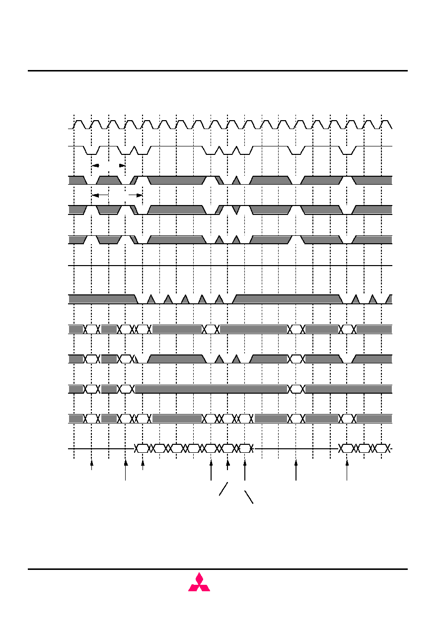
MH8S64AQFC -6,-6L,-7,-7L,-8,-8L
536,870,912-BIT (8,388,608 - WORD BY 64-BIT)SynchronousDRAM
MITSUBISHI LSIs
( / 55 )
22.Sep.2000
MIT-DS-0374-0.3
MITSUBISHI
ELECTRIC
Preliminary Spec.
Some contents are subject to change without notice.
Write Interrupted by Precharge @BL=4
/CS
/RAS
/CAS
/WE
CKE
BA0,1
DQ
X
X
X
0
Y
0
D0
D0
D0
D0
ACT#0
WRITE#0
0
1
2
3
4
5
6
7
8
9
10
11
12
13
14
15
16
17
tRCD
WRITE#1
CLK
X
X
X
1
tRRD
1
D1
D1
D1
D1
D1
ACT#1
Y
1
1
Y
Burst Write is not interrupted
by Precharge of the other bank.
0
X
X
X
1
PRE#1
PRE#0
ACT#1
WRITE#1
Burst Write is interrupted by
Precharge of the same bank.
Italic parameter indicates minimum case
A0-8
A10
DQM
A9,11
45
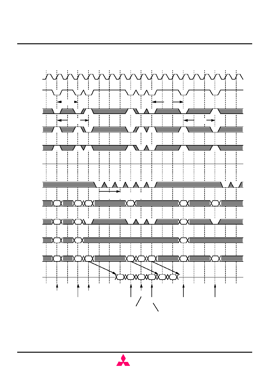
MH8S64AQFC -6,-6L,-7,-7L,-8,-8L
536,870,912-BIT (8,388,608 - WORD BY 64-BIT)SynchronousDRAM
MITSUBISHI LSIs
( / 55 )
22.Sep.2000
MIT-DS-0374-0.3
MITSUBISHI
ELECTRIC
Preliminary Spec.
Some contents are subject to change without notice.
Read Interrupted by Precharge @BL=4 CL=3
/CS
/RAS
/CAS
/WE
CKE
BA0,1
DQ
X
X
X
0
Y
0
Q0
Q0
Q0
ACT#0
READ#0
0
1
2
3
4
5
6
7
8
9
10
11
12
13
14
15
16
17
tRCD
Y
1
PRE#1
CLK
X
X
X
1
tRRD
Q1
Q1
ACT#1
PRE#0
Q0
DQM read latency=2
1
Y
1
Burst Read is not interrupted
by Precharge of the other bank.
0
X
X
X
1
tRCD
tRP
READ#1
ACT#1
READ#1
Burst Read is interrupted
by Precharge of the same bank.
Italic parameter indicates minimum case
A0-8
A10
DQM
A9,11
46
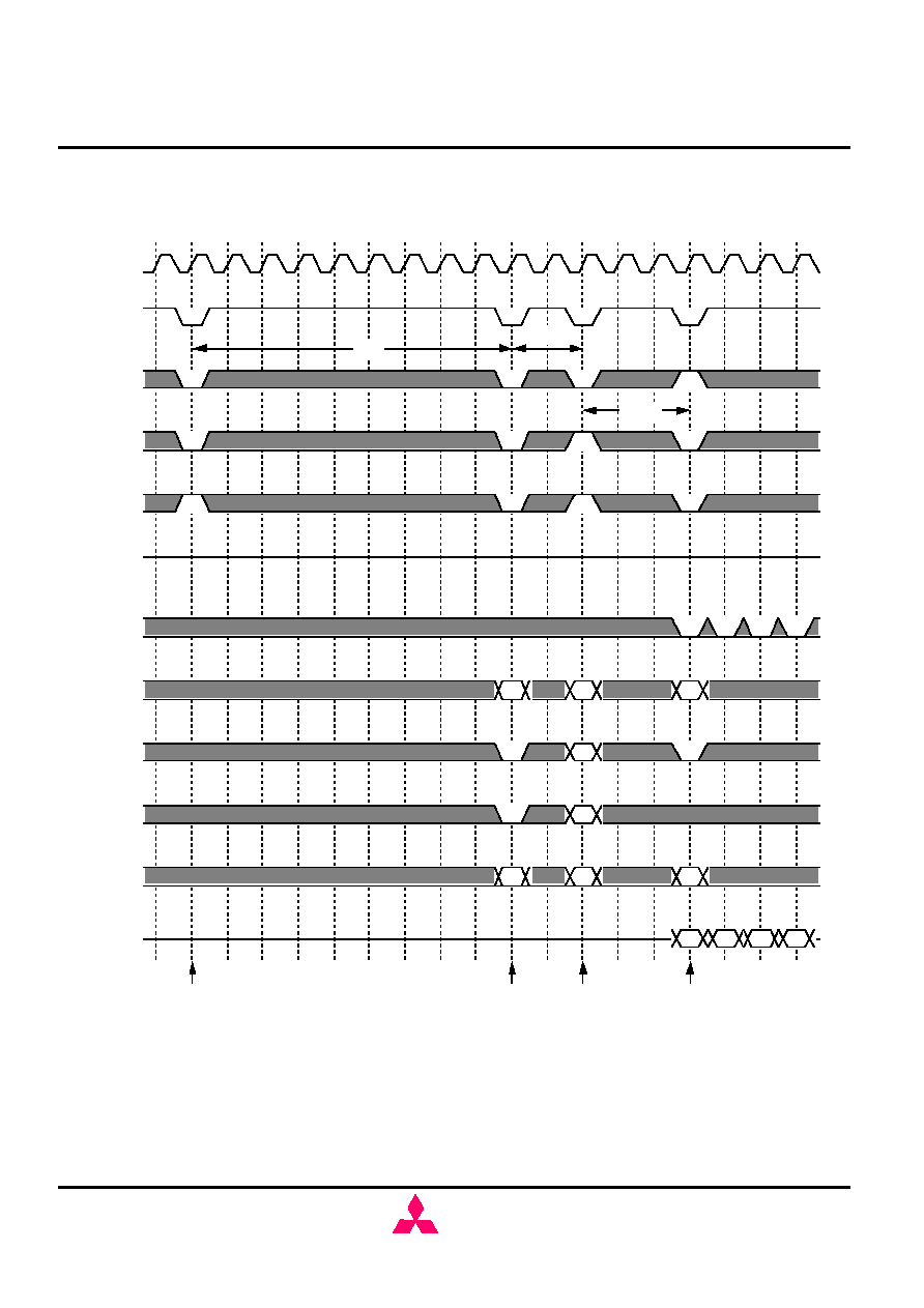
MH8S64AQFC -6,-6L,-7,-7L,-8,-8L
536,870,912-BIT (8,388,608 - WORD BY 64-BIT)SynchronousDRAM
MITSUBISHI LSIs
( / 55 )
22.Sep.2000
MIT-DS-0374-0.3
MITSUBISHI
ELECTRIC
Preliminary Spec.
Some contents are subject to change without notice.
Mode Register Setting
/CS
/RAS
/CAS
/WE
CKE
BA0,1
DQ
Auto-Ref (last of 8 cycles)
0
1
2
3
4
5
6
7
8
9
10
11
12
13
14
15
16
17
Y
0
CLK
tRC
D0
Mode
Register
Setting
M
0
X
X
X
0
tRCD
tRSC
ACT#0
WRITE#0
D0
D0
D0
Italic parameter indicates minimum case
A0-8
A10
DQM
A9,11
47
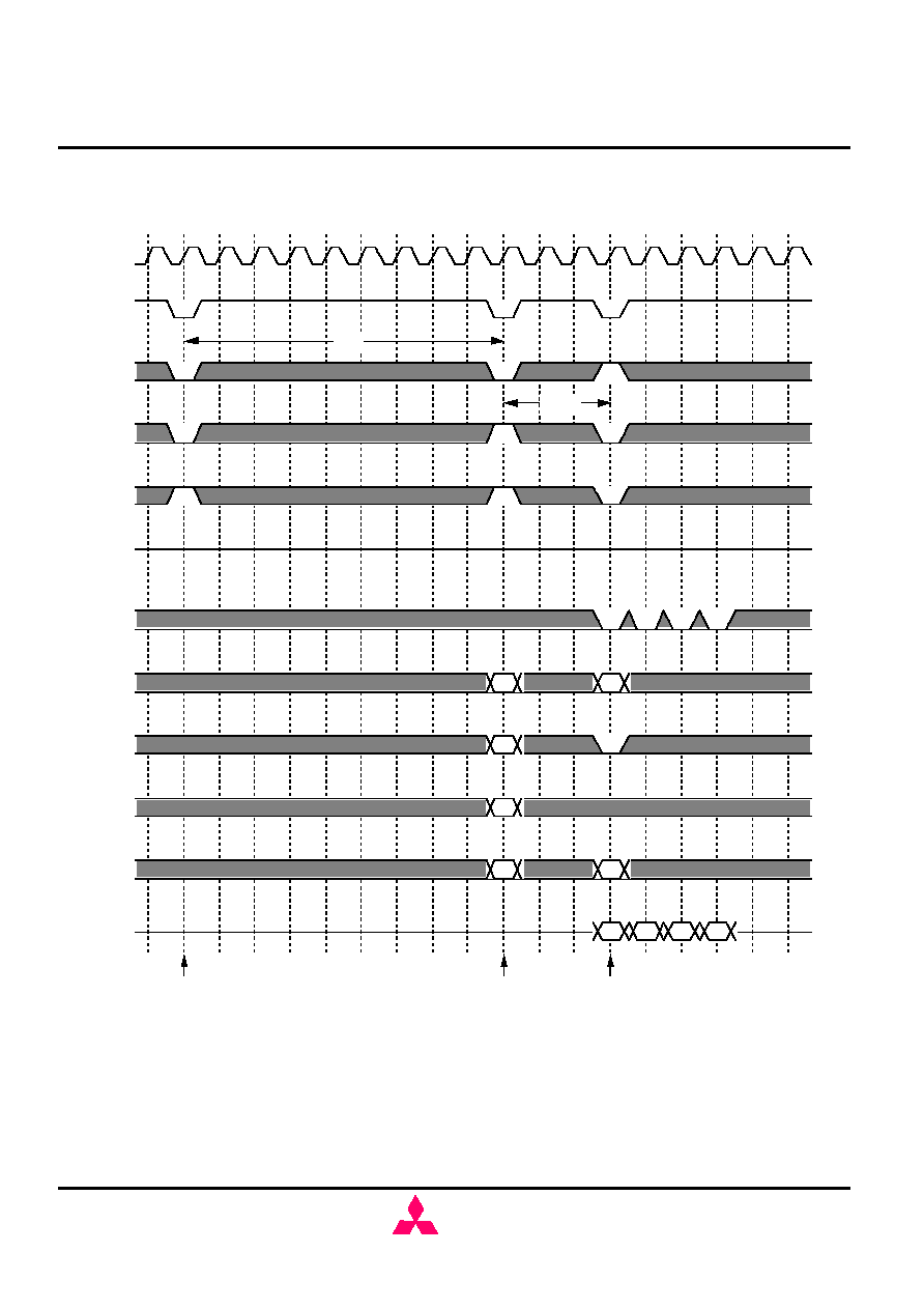
MH8S64AQFC -6,-6L,-7,-7L,-8,-8L
536,870,912-BIT (8,388,608 - WORD BY 64-BIT)SynchronousDRAM
MITSUBISHI LSIs
( / 55 )
22.Sep.2000
MIT-DS-0374-0.3
MITSUBISHI
ELECTRIC
Preliminary Spec.
Some contents are subject to change without notice.
Auto-Refresh @BL=4
/CS
/RAS
/CAS
/WE
CKE
BA0,1
DQ
Auto-Refresh
0
1
2
3
4
5
6
7
8
9
10
11
12
13
14
15
16
17
CLK
tRC
Before Auto-Refresh,
all banks must be idle state.
Y
0
D0
X
X
X
0
tRCD
ACT#0
WRITE#0
D0
D0
D0
After tRC from Auto-Refresh,
all banks are idle state.
Italic parameter indicates minimum case
A0-8
A10
DQM
A9,11
48
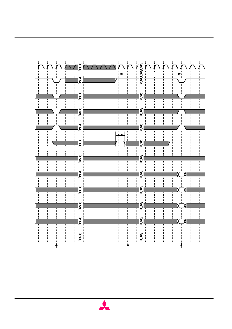
MH8S64AQFC -6,-6L,-7,-7L,-8,-8L
536,870,912-BIT (8,388,608 - WORD BY 64-BIT)SynchronousDRAM
MITSUBISHI LSIs
( / 55 )
22.Sep.2000
MIT-DS-0374-0.3
MITSUBISHI
ELECTRIC
Preliminary Spec.
Some contents are subject to change without notice.
Self-Refresh
/CS
/RAS
/CAS
/WE
CKE
BA0,1
DQ
Self-Refresh Entry
0
1
2
3
4
5
6
7
8
9
10
11
12
13
14
15
16
17
CLK
Before Self-Refresh Entry,
all banks must be idle state.
X
X
X
0
Self-Refresh Exit
ACT#0
After tRC from Self-Refresh Exit,
all banks are idle state.
tRC
tSRX
CLK can be stopped
CKE must be low to maintain Self-Refresh
Italic parameter indicates minimum case
A0-8
A10
DQM
A9,11
49
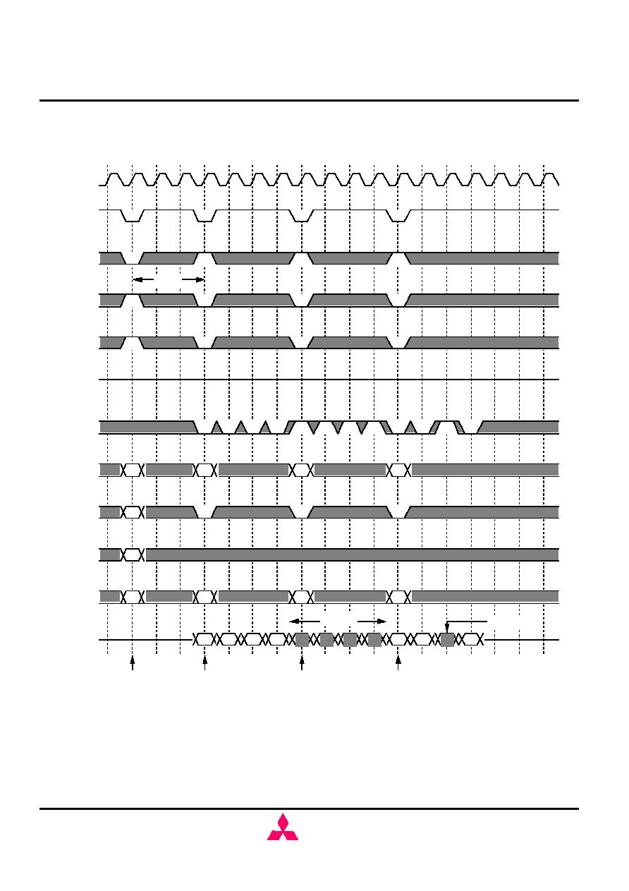
MH8S64AQFC -6,-6L,-7,-7L,-8,-8L
536,870,912-BIT (8,388,608 - WORD BY 64-BIT)SynchronousDRAM
MITSUBISHI LSIs
( / 55 )
22.Sep.2000
MIT-DS-0374-0.3
MITSUBISHI
ELECTRIC
Preliminary Spec.
Some contents are subject to change without notice.
DQM Write Mask @BL=4
/CS
/RAS
/CAS
/WE
CKE
BA0,1
DQ
X
X
X
0
Y
0
0
D0
D0
D0
D0
Y
0
D0
D0
D0
ACT#0
WRITE#0
WRITE#0
WRITE#0
0
1
2
3
4
5
6
7
8
9
10
11
12
13
14
15
16
17
tRCD
CLK
Y
masked
masked
Italic parameter indicates minimum case
A0-8
A10
DQM
A9,11
50
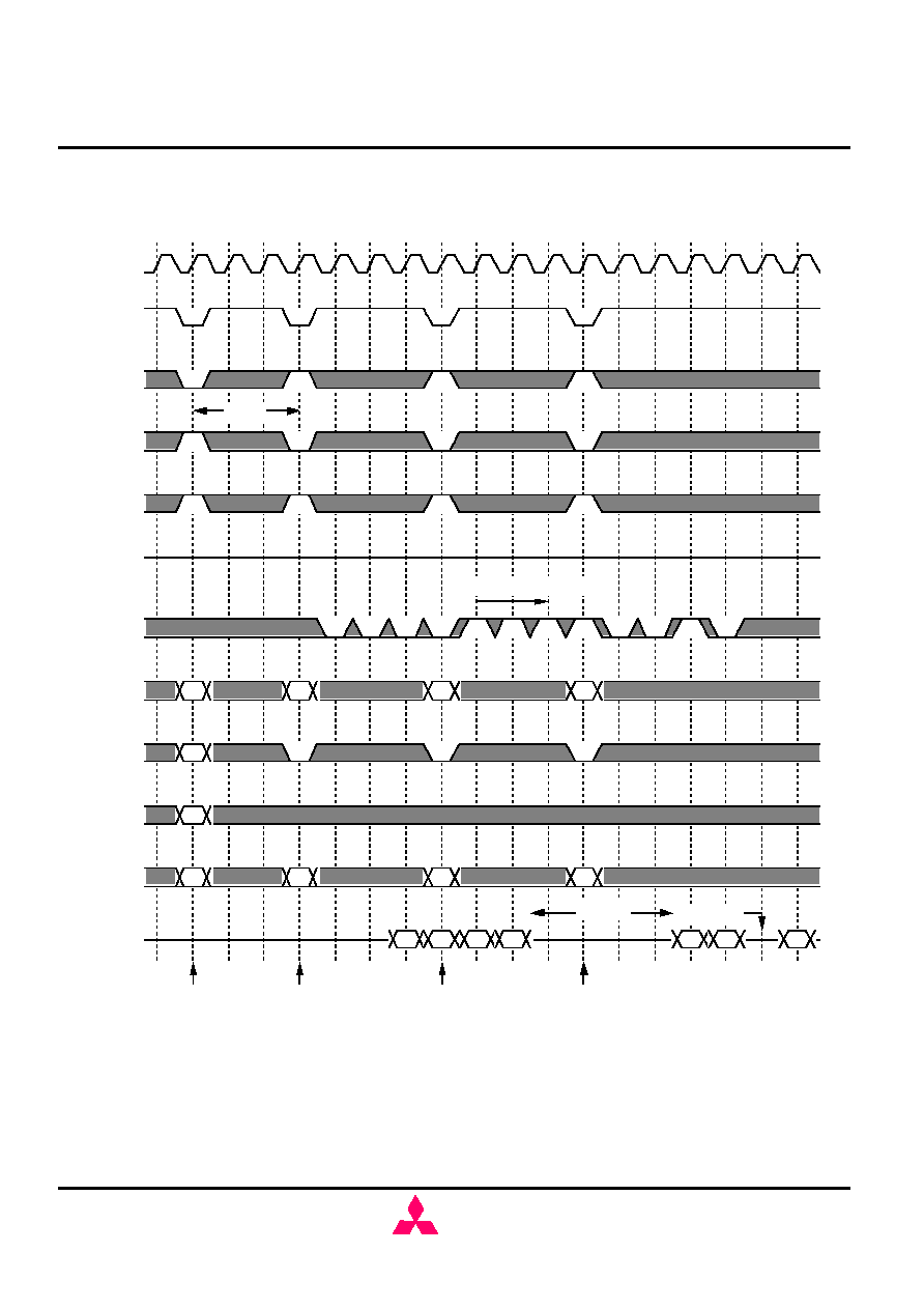
MH8S64AQFC -6,-6L,-7,-7L,-8,-8L
536,870,912-BIT (8,388,608 - WORD BY 64-BIT)SynchronousDRAM
MITSUBISHI LSIs
( / 55 )
22.Sep.2000
MIT-DS-0374-0.3
MITSUBISHI
ELECTRIC
Preliminary Spec.
Some contents are subject to change without notice.
DQM Read Mask @BL=4 CL=3
/CS
/RAS
/CAS
/WE
CKE
BA0,1
DQ
X
X
X
0
Y
0
0
Q0
Q0
Q0
Q0
Y
0
Q0
Q0
Q0
ACT#0
READ#0
READ#0
READ#0
0
1
2
3
4
5
6
7
8
9
10
11
12
13
14
15
16
17
tRCD
CLK
Y
masked
masked
DQM read latency=2
Italic parameter indicates minimum case
A0-8
A10
DQM
A9,11
51
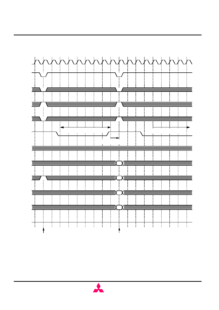
MH8S64AQFC -6,-6L,-7,-7L,-8,-8L
536,870,912-BIT (8,388,608 - WORD BY 64-BIT)SynchronousDRAM
MITSUBISHI LSIs
( / 55 )
22.Sep.2000
MIT-DS-0374-0.3
MITSUBISHI
ELECTRIC
Preliminary Spec.
Some contents are subject to change without notice.
Power Down
/CS
/RAS
/CAS
/WE
CKE
BA0,1
DQ
0
Precharge All
ACT#0
0
1
2
3
4
5
6
7
8
9
10
11
12
13
14
15
16
17
CLK
X
X
X
Standby Power Down
Active Power Down
CKE latency=1
Italic parameter indicates minimum case
A0-8
A10
DQM
A9,11
52
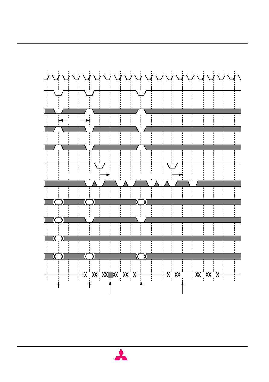
MH8S64AQFC -6,-6L,-7,-7L,-8,-8L
536,870,912-BIT (8,388,608 - WORD BY 64-BIT)SynchronousDRAM
MITSUBISHI LSIs
( / 55 )
22.Sep.2000
MIT-DS-0374-0.3
MITSUBISHI
ELECTRIC
Preliminary Spec.
Some contents are subject to change without notice.
CLK Suspend @BL=4 CL=3
/CS
/RAS
/CAS
/WE
CKE
BA0,1
DQ
X
X
X
0
Y
0
0
Q0
Q0
Q0
Q0
ACT#0
WRITE#0
READ#0
0
1
2
3
4
5
6
7
8
9
10
11
12
13
14
15
16
17
tRCD
CLK
Y
D0
D0
D0
D0
CLK suspended
CLK suspended
CKE latency=1
CKE latency=1
Italic parameter indicates minimum case
A0-8
A10
DQM
A9,11
53
MH8S64AQFC -6,-6L,-7,-7L,-8,-8L
536,870,912-BIT (8,388,608 - WORD BY 64-BIT)SynchronousDRAM
MITSUBISHI LSIs
( / 55 )
22.Sep.2000
MIT-DS-0374-0.3
MITSUBISHI
ELECTRIC
Preliminary Spec.
Some contents are subject to change without notice.
54
OUTLINE
20.00
31.75
4.00
6.00
MH8S64AQFC -6,-6L,-7,-7L,-8,-8L
536,870,912-BIT (8,388,608 - WORD BY 64-BIT)SynchronousDRAM
MITSUBISHI LSIs
( / 55 )
22.Sep.2000
MIT-DS-0374-0.3
MITSUBISHI
ELECTRIC
Preliminary Spec.
Some contents are subject to change without notice.
55
Keep safety first in your circuit designs!
Mitsubishi Electric Corporation puts the maximum effort into making semiconductor products
better and more reliable, but there is always the possibility that trouble may occur with them.
Trouble with semiconductors may lead to personal injury, fire or property damage.
Remember to give due consideration to safety when making your circuit designs, with
appropriate measures such as (i) placement of substitutive, auxiliary circuits, (ii) use of non-
flammable material or (iii) prevention against any malfunction or mishap.
Notes regarding these materials
1.These materials are intended as a reference to assist our customers in the selection of the
Mitsubishi semiconductor product best suited to the customer's application; they do not
convey any license under any intellectual property rights, or any other rights, belonging to
Mitsubishi Electric Corporation or a third party.
2.Mitsubishi Electric Corporation assumes no responsibility for any damage, or infringement
of any third-party's rights, originating in the use of any product data, diagrams, charts,
programs, algorithms, or circuit application examples contained in these materials.
3.All information contained in these materials, including product data, diagrams, charts,
programs and algorithms represents information on products at the time of publication of
these materials, and are subject to change by Mitsubishi Electric Corporation without notice
due to product improvements or other reasons. It is therefore recommended that customers
contact Mitsubishi Electric Corporation or an authorized Mitsubishi Semiconductor product
distributor for the latest product information before purchasing a product listed herein.
The information described here may contain technical inaccuracies or typographical errors.
Mitsubishi Electric Corporation assumes no responsibility for any damage, liability, or other
loss rising from these inaccuracies or errors.
Please also pay attention to information published by Mitsubishi Electric Corporation by
various means, including the Mitsubishi Semiconductor home page
(http://www.mitsubishichips.com).
4.When using any or all of the information contained in these materials, including product
data, diagrams, charts, programs and algorithms, please be sure to evaluate all information
as a total system before making a final decision on the applicability of the information and
products.
Mitsubishi Electric Corporation assumes no responsibility for any damage, liability or other
loss resulting from the information contained herein.
5.Mitsubishi Electric Corporation semiconductors are not designed or manufactured for use in
a device or system that is used under circumstances in which human life is potentially at stake.
Please contact Mitsubishi Electric Corporation or an authorized Mitsubishi Semiconductor
product distributor when considering the use of a product contained herein for any specific
purposes, such as apparatus or systems for transportation, vehicular, medical, aerospace,
nuclear, or undersea repeater use.
6.The prior written approval of Mitsubishi Electric Corporation is necessary to reprint or
reproduce in whole or in part these materials.
7.If these products or technologies are subject to the Japanese export control restrictions, they
must be exported under a license from the Japanese government and cannot be imported
into a country other than the approved destination.
Any diversion or reexport contrary to the export control laws and regulations of Japan and/or
the country of destination is prohibited.
8.Please contact Mitsubishi Electric Corporation or an authorized Mitsubishi Semiconductor
product distributor for further details on these materials or the products contained therein.