
Sep.1998
6.0 Introduction to Intelligent
Power Modules (IPM)
Mitsubishi Intelligent Power Mod-
ules (IPMs) are advanced hybrid
power devices that combine high
speed, low loss IGBTs with opti-
mized gate drive and protection cir-
cuitry. Highly effective over-current
and short-circuit protection is real-
ized through the use of advanced
current sense IGBT chips that al-
low continuous monitoring of power
device current. System reliability is
further enhanced by the IPM's inte-
grated over temperature and under
voltage lock out protection. Com-
pact, automatically assembled In-
telligent Power Modules are de-
signed to reduce system size, cost,
and time to market. Mitsubishi
Electric introduced the first full line
of Intelligent Power Modules in No-
vember, 1991. Continuous im-
provements in power chip, packag-
ing, and control circuit technology
have lead to the IPM lineup shown
in Table 6.1.
6.0.1 Third Generation Intelli-
gent Power Modules
Mitsubishi third generation intelli-
gent power module family shown in
Table 6.1 represents the industries
most complete line of IPMs. Since
their original introduction in 1993
the series has been expanded to
include 36 types with ratings rang-
ing from 10A 600V to 800A 1200V.
The power semiconductors used in
these modules are based on the
field proven H-Series IGBT and di-
ode processes. In Table 6.1 the
third generation family has been di-
vided into two groups, the "Low
Profile Series" and "High Power
Series" based on the packaging
technology that is used. The third
generation IPM has been optimized
for minimum switching losses in or-
der to meet industry demands for
acoustically noiseless inverters
with carrier frequencies up to
20kHz. The built in gate drive and
protection has been carefully de-
signed to minimize the components
required for the user supplied inter-
face circuit.
6.0.2 V-Series High Power IPMs
The V-Series IPM was developed
in order to address newly emerging
industry requirements for higher re-
liability, lower cost and reduced
EMI. By utilizing the low inductance
packaging technology developed
for the U-Series IGBT module (de-
scribed in Section 4.1.5) combined
with an advanced super soft free-
wheel diode and optimized gate
drive and protection circuits the V-
Series IPM family achieves im-
proved performance at reduced
cost. The detailed descriptions of
IPM operation and interface re-
quirements presented in Sections
6.1 through 6.8 apply to V-Series
as well as third generation IPMs.
The only exception being that V-
Series IPMs have a unified short
circuit protection function that takes
the place of the separate short cir-
cuit and over current functions de-
scribed in Sections 6.4.4 and 6.4.5.
The unified protection was made
Third Generation Low Profile Series - 600V
PM10CSJ060
10
Six IGBTs
PM15CSJ060
15
Six IGBTs
PM20CSJ060
20
Six IGBTs
PM30CSJ060
30
Six IGBTs
PM50RSK060
50
Six IGBTs + Brake ckt.
PM75RSK060
75
Six IGBTs + Brake ckt.
Third Generation Low Profile Series - 1200V
PM10CZF120
10
Six IGBTs
PM10RSH120
10
Six IGBTs + Brake ckt.
PM15CZF120
15
Six IGBTs
PM15RSH120
15
Six IGBTs + Brake ckt.
PM25RSK120
25
Six IGBTs + Brake ckt.
Third Generation High Power Series - 600V
PM75RSA060
75
Six IGBTs + Brake ckt.
PM100CSA060 100
Six IGBTs
PM100RSA060 100
Six IGBTs + Brake ckt.
PM150CSA060 150
Six IGBTs
PM150RSA060 150
Six IGBTs + Brake ckt.
PM200CSA060 200
Six IGBTs
PM200RSA060 200
Six IGBTs + Brake ckt.
PM200DSA060 200
Two IGBTs: Half Bridge
PM300DSA060 300
Two IGBTs: Half Bridge
PM400DAS060 400
Two IGBTs: Half Bridge
PM600DSA060 600
Two IGBTs: Half Bridge
PM800HSA060 800
One IGBT
Third Generation High Power Series - 1200V
PM25RSB120
25
Six IGBTs + Brake ckt.
PM50RSA120
50
Six IGBTs + Brake ckt.
PM75CSA120
75
Six IGBTs
PM75DSA120
75
Two IGBTs: Half Bridge
PM100CSA120 100
Six IGBTs
PM100DSA120 100
Two IGBTs: Half Bridge
PM150DSA120 150
Two IGBTs: Half Bridge
PM200DSA120 200
Two IGBTs: Half Bridge
PM300DSA120 300
Two IGBTs: Half Bridge
PM400HSA120 400
Two IGBTs: Half Bridge
PM600HSA120 600
One IGBT
PM800HSA120 800
One IGBT
V-Series High Power - 600V
PM75RVA060
75
Six IGBTs + Brake ckt.
PM100CVA060 100
Six IGBTs
PM150CVA060 150
Six IGBTs
PM200CVA060 200
Six IGBTs
PM300CVA060 300
Six IGBTs
PM400DVA060 400
Two IGBTs: Half Bridge
PM600DVA060 600
Two IGBTs: Half Bridge
V-Series High Power - 1200V
PM50RVA120
50
Six IGBTs + Brake ckt.
PM75CVA120
75
Six IGBTs
PM100CVA120 100
Six IGBTs
PM150CVA120 150
Six IGBTs
PM200DVA120 200
Two IGBTs: Half Bridge
PM300DVA120 300
Two IGBTs: Half Bridge
Type Number
Amps Power Circuit
Type Number
Amps Power Circuit
Table 6.1 Mitsubishi Intelligent Power Modules
MITSUBISHI SEMICONDUCTORS POWER MODULES MOS
USING INTELLIGENT POWER MODULES
Sep.1998
possible by an advanced RTC
(Real Time Control) current clamp-
ing circuit that eliminates the need
for the over current protection func-
tion. In V-Series IPMs a unified
short circuit protection with a delay
to avoid unwanted operation re-
places the over current and short
circuit modes of the third genera-
tion devices.
6.1 Structure of Intelligent
Power Modules
Mitsubishi Intelligent Power Mod-
ules utilize many of the same field
proven module packaging tech-
nologies used in Mitsubishi IGBT
modules. Cost effective implemen-
tation of the built in gate drive and
protection circuits over a wide
range of current ratings was
achieved using two different pack-
aging techniques. Low power de-
vices use a multilayer epoxy isola-
tion system while medium and high
power devices use ceramic isola-
tion. These packaging technologies
are described in more detail in Sec-
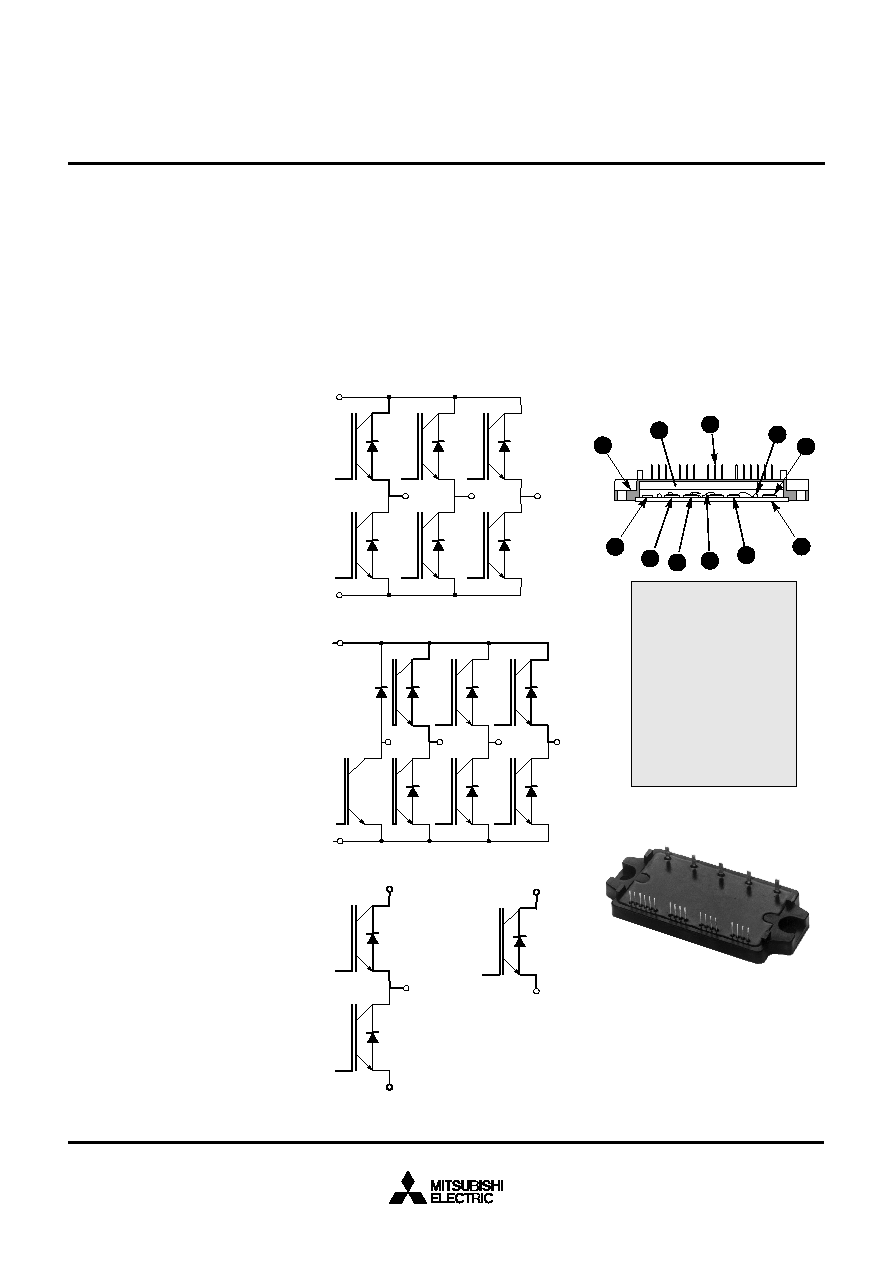
tions 6.1.1 and 6.1.2. IPM are
available in four power circuit con-
figurations, single (H), dual (D), six
pack (C), and seven pack (R).
Table 6.1 indicates the power cir-
cuit of each IPM and Figure 6.1
shows the power circuit configura-
tions.
6.1.1 Multilayer Epoxy Construc-
tion
Low power IPM (10-50A, 600V and
10-15A, 1200V) use a multilayer
epoxy based isolation system. In
this system, alternate layers of cop-
per and epoxy are used to create a
shielded printed circuit directly on
the aluminum base plate. Power
chips and gate control circuit com-
ponents are soldered directly to the
substrate eliminating the need for a
separate printed circuit board and
ceramic isolation materials. Mod-
ules constructed using this tech-
nique are easily identified by their
extremely low profile packages.
This package design is ideally
suited for consumer and industrial
applications where low cost and
compact size are important.
Figure 6.2 shows a cross section
of this type of IPM package. Figure
6.3 is a PM20CSJ060 20A, 600V
IPM.
P
U
V
W
C2E1
C1
E2
E
C
N
TYPE C
TYPE D
TYPE H
P
N
U
TYPE R
V
W
B
Figure 6.2
Multi-Layer Epoxy
Construction
Figure 6.1
Power Circuit
Configuration
Figure 6.3
PM20CSJ060
1.
2.
3.
4.
5.
6.
7.
8.
9.
10.
11.
Case
Epoxy Resin
Input Signal Terminal
SMT Resistor
Gate Control IC
SMT Capacitor
IGBT Chip
Free-wheel Diode Chip
Bond Wire
Copper Block
Baseplate with Epoxy
Based Isolation
11
10
9
8
6
7
1
2
3
4
5
MITSUBISHI SEMICONDUCTORS POWER MODULES MOS
USING INTELLIGENT POWER MODULES
Sep.1998
6.1.2 Ceramic Isolation Con-
struction
Higher power IPMs are constructed
using ceramic isolation material. A
direct bond copper process in
which copper patterns are bonded
directly to the ceramic substrate
without the use of solder is used in
these modules. This substrate pro-
vides the improved thermal charac-
teristics and greater current carry-
ing capabilities that are needed in
these higher power devices. Gate
drive and control circuits are con-
tained on a separate PCB mounted
directly above the power devices.
The PCB is a multilayer construc-
tion with special shield layers for
EMI noise immunity. Figure 6.4
shows the structure of a ceramic
isolated Intelligent Power Module.
Figure 6.5 is a PM75RSA060 75 A,
600V IPM.
Figure 6.4 Ceramic Isolation Construction
Figure 6.5 PM75RSA060
SILICON CHIP
DBC PLATE
BASE
PLATE
SILICON GEL
CASE
MAIN
TERMINAL
EPOXY
RESIN
GUIDE
PIN
INPUT SIGNAL
TERMINAL
INTERCONNECT
TERMINAL
ELECTRODE
ALUMINUM WIRE
SHIELD
LAYER
RESISTOR
CONTROL BOARD
PCB
SHIELD
LAYER
SIGNAL
TRACE
MITSUBISHI SEMICONDUCTORS POWER MODULES MOS
USING INTELLIGENT POWER MODULES
Sep.1998
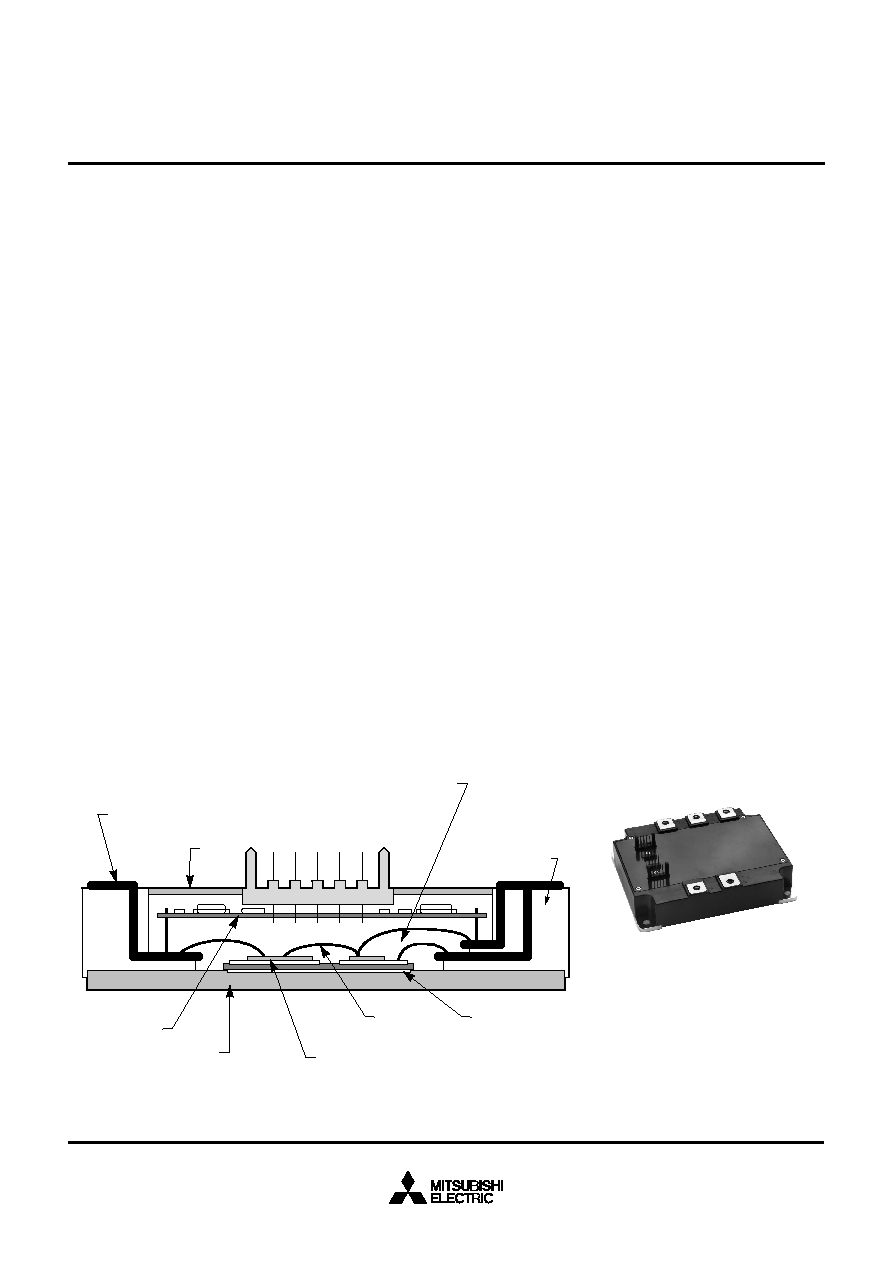
6.1.3 V-Series IPM Construction
V-Series IPMs are similar to the ce-
ramic isolated types described
in Section 6.1.2 except that an in-
sert molded case similar to the
U-Series IGBT is used. Like the
U-Series IGBT described in Sec-
tion 4.1.5, the V-Series IPM
has lower internal inductance and
improved power cycle durability.
Figure 6.6 is a cross section draw-
ing showing the construction of the
V-Series IPM. The insert molded
case makes the V-Series IPM is
easier to manufacture and lower in
cost. Figure 6.7 shows a
PM150CVA120 which is a 150A
1200V V-Series IPM.
6.1.4 Advantages of Intelligent
Power Module
IPM (Intelligent Power Module)
products were designed and devel-
oped to provide advantages to
Customers by reducing design, de-
velopment, and manufacturing
costs as well as providing improve-
ment in system performance and
reliability over conventional IGBTs.
Design and development effort is
simplified and successful drive co-
ordination is assured by the inte-
gration of the drive and protection
circuitry directly into the IPM. Re-
duced time to market is only one of
the additional benefits of using an
IPM. Others include increased sys-
tem reliability through automated
IPM assembly and test and reduc-
tion in the number of components
that must be purchased, stored,
and assembled. Often the system
size can be reduced through
smaller heatsink requirements as a
result of lower on-state and switch-
ing losses. All IPMs use the same
standardized gate control interface
with logic level control circuits al-
lowing extension of the product line
without additional drive circuit de-
sign. Finally, the ability of the IPM
to self protect in fault situations re-
duce the chance of device destruc-
tion during development testing as
well as in field stress situations.
6.2 IPM Ratings and Characteris-
tics
IPM datasheets are divided into
three sections:
∑
Maximum Ratings
∑
Characteristics (electrical,
thermal, mechanical)
∑
Recommended Operating
Conditions
The limits given as maximum rating
must not be exceeded under any
circumstances, otherwise destruc-
tion of the IPM may result.
Key parameters needed for system
design are indicated as electrical,
thermal, and mechanical character-
istics.
The given recommended operating
conditions and application circuits
should be considered as a prefer-
able design guideline fitting most
applications.
POWER TERMINALS
SILICONE GEL
COVER
INSERT MOLD CASE
DBC AIN CERAMIC
SUBSTRATE
SILICON CHIPS
BASE PLATE
PRINTED CIRCUIT
BOARD
ALUMINUM
BOND WIRES
SIGNAL TERMINALS
Figure 6.6
V-Series IPM Construction
Figure 6.7
PM150CVA120
MITSUBISHI SEMICONDUCTORS POWER MODULES MOS
USING INTELLIGENT POWER MODULES

Sep.1998
6.2.1 Maximum Ratings
Symbol
Parameter
Definition
Inverter Part
V
CC
Supply Voltage
Maximum DC bus voltage applied between P-N
V
CES
Collector-Emitter Voltage
Maximum off-state collector-emitter voltage at applied control input off signal
±
I
C
Collector-Current
Maximum DC collector and FWDi current @ T
j
150
∞
C
±
I
CP
Collector-Current (peak)
Maximum peak collector and FWDi current @ T
j
150
∞
C
P
C
Collector Dissipation
Maximum power dissipation per IGBT switch at T
j
= 25
∞
C
T
j
Junction Temperature
Range of IGBT junction temperature during operation
Brake Part
V
R(DC)
FWDi Reverse Voltage
Maximum reverse voltage of FWDi
I
F
FWDi Forward Current
Maximum FWDi DC current at T
j
150
∞
C
Control Part
V
D
Supply Voltage
Maximum control supply voltage
V
CIN
Input Voltage
Maximum voltage between input (I) and ground (C) pins
V
FO
Fault Output Supply Voltage
Maximum voltage between fault output (FO) and ground (C) pins
I
FO
Fault Output Current
Maximum sink current of fault output (FO) pin
Total System
V
CC(prot)
Supply Voltage Protected
Maximum DC bus voltage applied between P-N with guaranteed OC and SC protection
by OC & SC
T
C
Module Case Operating
Range of allowable case temperature at specified reference point during operation
Temperature
T
stg
Storage Temperature
Range of allowable ambient temperature without voltage or current
V
iso
Isolation Voltage
Maximum isolation voltage (AC 60Hz 1 min.) between baseplate and module terminals
(all main and signal terminals externally shorted together)
6.2.2 Thermal Resistance
Symbol
Parameter
Definition
R
th(j-c)
Junction to Case
Maximum value of thermal resistance between junction and case per switch
Thermal Resistance
R
th(c-f)
Contact Thermal
Maximum value of thermal resistance between case and fin (heatsink) per IGBT/FWDi pair
Resistance
with thermal grease applied according to mounting recommendations
6.2.3 Electrical Characteristics
Symbol
Parameter
Definition
Inverter and Brake Part
V
CE
(sat)
Collector-Emitter
IGBT on-state voltage at rated collector current under specified conditions
Saturation Voltage
V
EC
FWDi Forward Voltage
FWDi forward voltage at rated current under specified conditions
t
on
Turn-On Time
t
rr
FWDi Recovery Time
Inductive load switching times under rated conditions
t
c(on)
Turn-On Crossover Time
(See Figure 6.10)
t
off
Turn-Off Time
t
c(off)
Turn-Off Crossover Time
I
CES
Collector-Emitter Cutoff
Collector-Emitter current in off-state at V
CE
= V
CES
under specified conditions
MITSUBISHI SEMICONDUCTORS POWER MODULES MOS
USING INTELLIGENT POWER MODULES
Sep.1998
The following test circuits are used
to evaluate the IPM characteristics.
1.
V
CE
(sat) and V
EC
To ensure specified junction
temperature, T
j,
measurements
of V
CE
(sat) and V
EC
must be
performed as low duty factor
pulsed tests. (See Figures 6.8
and 6.9)
6.2.3 Electrical Characteristics (continued)
Symbol
Parameter
Definition
Control Part
V
D
Supply Voltage
Range of allowable control supply voltage in switching operation
I
D
Circuit Current
Control supply current in stand-by mode
V
CIN(on)
Input ON-Voltage
A voltage applied between input (I) and ground (C) pins less than this value will turn on the IPM
V
CIN(off)
Input OFF-Voltage
A voltage applied between input (I) and ground (C) pins higher than this value will turn off the IPM
f
PWM
PWM Input Frequency
Range of PWM frequency for VVVF inverter operations
t
dead
Arm Shoot Through
Time delay required between high and low side input off/on signals to prevent an
Blocking Time
arm shoot through
OC
Over-Current Trip Level
Collector that will activate the over-current protection
SC
Short-Circuit Trip Level
Collector current that will activate the short-circuit protection
t
off(OC)
Over-Current Delay Time
Time delay after collector current exceeds OC trip level until OC protection is activated
OT
Over-Temperature Trip Level
Baseplate temperature that will activate the over-temperature protection
OT
r
Over-Temperature
Temperature that the baseplate must fall below to reset an over-temperature fault
Reset Level
UV
Control Supply
Control supply voltage below this value will activate the undervoltage protection
Undervoltage Trip Level
UV
r
Control Supply
Control supply voltage that must exceed to reset an undervoltage fault
Undervoltage Reset Level
I
FO(H)
Fault Output Inactive Current
Fault output sink current when no fault has occurred
I
FO(L)
Fault Output Active Current
Fault Output sink current when a fault has occurred
t
FO
Fault Output Pulsed Width
Duration of the generated fault output pulse
V
SXR
SXR Terminal Output Voltage
Regulated power supply voltage on SXR terminal for driving the external optocoupler
6.2.4 Recommended Operation Conditions
Symbol
Parameter
Definition
V
CC
Main Supply Voltage
Recommended DC bus voltage range
V
D
Control Supply Voltage
Recommended control supply voltage range
V
CIN(on)
Input ON-Voltage
Recommended input voltage range to turn on the IPM
V
CIN(off)
Input OFF-Voltage
Recommended input voltage range to turn off the IPM
f
PWM
PWM Input Frequency
Recommended range of PWM carrier frequency using the recommended application circuit
t
DEAD
Arm Shoot Through
Recommended time delay between high and low side off/on signals to the optocouplers
Blocking Time
using the recommended application circuit
VX1
SXR
CX1
VXC
E1(E2)
C1(C2)
V
D
V
I
C
VX1
SXR
CX1
VXC
E1(E2)
C1(C2)
V
D
V
I
C
Figure 6.8 V
CE
(sat) Test
Figure 6.9 V
EC
Test
6.2.5 Test Circuits and Conditions
MITSUBISHI SEMICONDUCTORS POWER MODULES MOS
USING INTELLIGENT POWER MODULES
Sep.1998
2.
Half-Bridge Test Circuit and
Switching Time Definitions.
Figure 6.10 shows the stan-
dard half-bridge test circuit and
switching waveforms. Switch-
ing times and FWDi recovery
characteristics are defined as
shown in this figure.
3.
Overcurrent and
Short-Circuit Test
I
trip
levels and timing specifica-
tions in short circuit and
overcurrent are defined as
shown in Figure 6.11. By using
a fixed load resistance the sup-
ply voltage, V
CC
, is gradually
increased until OC and SC trip
levels are reached.
Precautions:
A. Before applying any main bus
voltage, V
CC
, the input termi-
nals should be pulled up by re-
sistors to their corresponding
control supply (or SXR) pin,
each input signal should be
kept in OFF state, and the con-
trol supply should be provided.
After this, the specified ON and
OFF level for each input signal
should be applied. The control
supply should also be applied
to the non-operating arm of the
module under test and inputs
of these arms should be kept
to their OFF state.
B. When performing OC and SC
tests the applied voltage, V
CC
,
must be less than V
CC(prot)
and the turn-off surge voltage
spike must not be allowed to
rise above the V
CES
rating of
the device. (These tests must
not be attempted using a
curve tracer.)
+
I
C
INTEGRATED
GATE
CONTROL
CIRCUIT
INTEGRATED
GATE
CONTROL
CIRCUIT
+
+
t
d (on)
I
CIN
(t
on
=
t
d
(
on
)
+
t
r
)
t
r
t
d (off)
(t
off
=
t
d
(off)
+
t
f
)
t
f
t
c (off)
t
c (on)
10%
90%
10%
90%
I
C
t
rr
I
rr
V
CE
I
C
V
CE
OFF
SIGNAL
ON
PULSE
V
CC
V
D
V
D
Figure 6.10
Half-Bridge Test Circuit and Switching Time Definitions
ON
PULSE
SC
OC
INPUT
SIGNAL
NORMAL
OPERATION
OVER
CURRENT
SHORT
CIRCUIT
V
C
ON
PULSE
R*
R IS SIZED TO CAUSE
SC AND OC CONDITIONS
*
V
CC
+
t
off
(OC)
I
C
INTEGRATED
GATE
CONTROL
CIRCUIT
SC
OC
SC
OC
I
C
I
C
I
C
Figure 6.11
Over-Current and Short-Circuit Test Circuit
MITSUBISHI SEMICONDUCTORS POWER MODULES MOS
USING INTELLIGENT POWER MODULES

Sep.1998
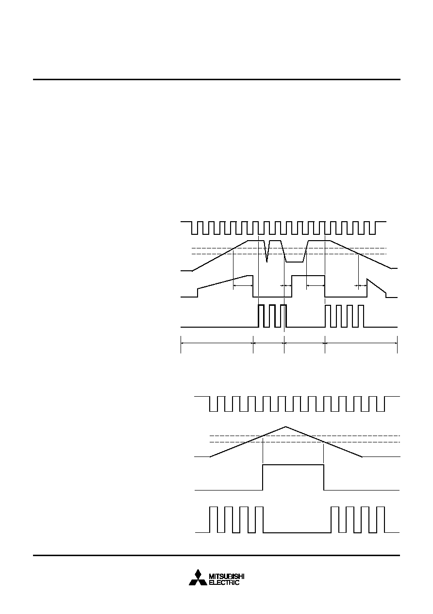
6.3 Area of Safe Operation for
Intelligent Power Modules
The IPMs built-in gate drive and
protection circuits protect it from
many of the operating modes that
would violate the Safe Operation
Area (SOA) of non-intelligent IGBT
modules. A conventional SOA defi-
nition that characterizes all pos-
sible combinations of voltage, cur-
rent, and time that would cause
power device failure is not re-
quired. In order to define the SOA
for IPMs, the power device capabil-
ity and control circuit operation
must both be considered. The re-
sulting easy to use short circuit and
switching SOA definitions for Intelli-
gent Power Modules are summa-
rized
in this section.
6.3.1 Switching SOA
Switching or turn-off SOA is nor-
mally defined in terms of the maxi-
mum allowable simultaneous volt-
age and current during repetitive
turn-off switching operations. In the
case of the IPM the built-in gate
drive eliminates many of the dan-
gerous combinations of voltage
and current that are caused by im-
proper gate drive. In addition, the
maximum operating current is lim-
ited by the over current protection
circuit. Given these constraints the
switching SOA can be defined us-
ing the waveform shown in Figure
6.12. This waveform shows that the
IPM will operate safely as long as
the DC bus voltage is below the
data sheet V
CC(prot)
specification,
the turn-off transient voltage across
C-E terminals of each IPM switch is
maintained below the V
CES
specifi-
cation, T
j
is less than 125
∞
C, and
the control power supply voltage is
between 13.5V and 16.5V. In this
waveform I
OC
is the maximum cur-
rent that the IPM will allow without
causing an Over Current (OC) fault
to occur. In other words, it is just
below the OC trip level. This wave-
form defines the worst case for
hard turn-off operations because
the IPM will initiate a controlled
slow shutdown for currents higher
than the OC
trip level.
6.3.2 Short Circuit SOA
The waveform in Figure 6.13 de-
picts typical short circuit operation.
The standard test condition uses a
minimum impedance short circuit
which causes the maximum short
circuit current to flow in the device.
In this test, the short circuit current
(I
SC
) is limited only by the device
characteristics. The IPM is guaran-
teed to survive non-repetitive short
circuit and over current conditions
as long as the initial DC bus volt-
age is less than the V
CC(prot)
specification, all transient voltages
across C-E terminals of each IPM
switch are maintained less than the
V
CES
specification, T
j
is less than
125
∞
C, and the control supply volt-
age is between 13.5V and 16.5V.
The waveform shown depicts the
controlled slow shutdown that is
used by the IPM in order to help
minimize transient voltages.
Note:
The condition V
CE
V
CES
has to
be carefully checked for each IPM
switch. For easing the design an-
other rating is given on the data
sheets, V
CC(surge)
, i.e., the maxi-
mum allowable switching surge
voltage applied between the P and
N terminals.
6.3.3 Active Region SOA
Like most IGBTs, the IGBTs used in
the IPM are not suitable for linear
or active region operation. Nor-
mally device capabilities in this
mode of operation are described in
terms of FBSOA (Forward Biased
Safe Operating Area). The IPM's
internal gate drive forces the IGBT
to operate with a gate voltage of ei-
ther zero for the off state or the
control supply voltage (V
D
) for the
on state. The IPMs under-voltage
lock out prevents any possibility of
active or linear operation by auto-
matically turning the power device
off if V
D
drops to a level
that could cause desaturation of
the IGBT.
Figure 6.13
Short-Circuit
Operation
Figure 6.12
Turn-Off Waveform
I
OC
V
CES
V
CC(PROT)
t
off(OC)
V
CES
V
CES
V
CC(PROT)
I
SC
MITSUBISHI SEMICONDUCTORS POWER MODULES MOS
USING INTELLIGENT POWER MODULES

Sep.1998
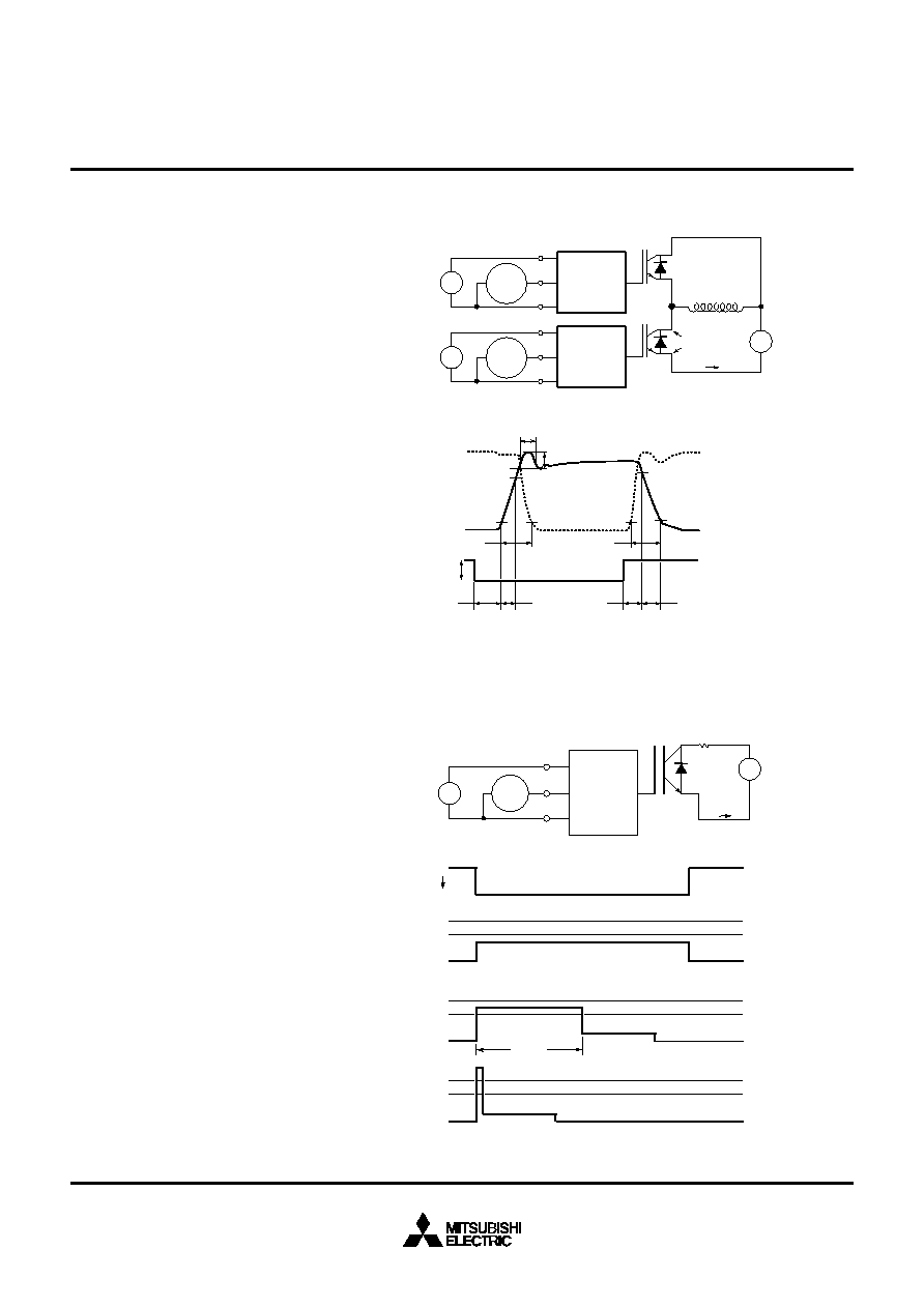
6.4. IPM Self Protection
6.4.1 Self Protection Features
IPM (Intelligent Power Modules)
have sophisticated built-in protec-
tion circuits that prevent the power
devices from being damaged
should the system malfunction or
be over stressed. Our design and
applications engineers have devel-
oped fault detection and shut down
schemes that allow maximum utili-
zation of power device capability
without compromising reliability.
Control supply under-voltage, over-
temperature, over-current, and
short-circuit protection are all pro-
vided by the IPM's internal gate
control circuits. A fault output signal
is provided to alert the system con-
troller if any of the protection cir-
cuits are activated. Figure 6.14 is a
block diagram showing the IPMs
internally integrated functions. This
diagram also shows the isolated in-
terface circuits and control power
supply that must be provided by
the user. The internal gate control
circuit requires only a simple +15V
DC supply. Specially designed gate
drive circuits eliminate the need for
a negative supply to off bias the
IGBT. The IPM control input is de-
signed to interface with
optocoupled transistors with a mini-
mum of external components. The
operation and timing of each pro-
tection feature is described in Sec-
tions 6.4.2 through 6.4.5.
6.4.2 Control Supply
Under-Voltage Lock-Out
The Intelligent Power Module's in-
ternal control circuits operate from
an isolated 15V DC supply. If, for
any reason, the voltage of this sup-
ply drops below the specified un-
der-voltage trip level (UV
t
), the
power devices will be turned off
and a fault signal will be generated.
Small glitches less than the speci-
fied t
dUV
in length will not affect the
operation of the control circuitry
and will be ignored by the under-
voltage protection circuit. In order
for normal operation to resume, the
supply voltage must exceed the un-
der-voltage reset level (UV
r
). Op-
eration of the under-voltage protec-
tion circuit will also occur during
power up and power down of the
control supply. This operation is
normal and the system controller's
program should take the fault out-
put delay (t
fo
) into account. Figure
6.15 is a timing diagram showing
the operation of the under-voltage
lock-out protection circuit. In this
diagram an active low input signal
is applied to the input pin of the
IPM by the system controller. The
effects of control supply power up,
power down and failure on the
power device gate drive and fault
output are shown.
Caution:
1.
Application of the main bus
voltage at a rate greater than
20V/
µ
s before the control
power supply is on and stabi-
lized may cause destruction of
the power devices.
2.
Voltage ripple on the control
power supply with dv/dt in ex-
cess of 5V/
µ
s may cause a
false trip of the UV lock-out.
6.4.3 Over-Temperature
Protection
The Intelligent Power Module has a
temperature sensor mounted on
the isolating base plate near the
IGBT chips. If the temperature of
the base plate exceeds the over-
temperature trip level (OT) the
IPMs internal control circuit will
protect the power devices by dis-
abling the gate drive and ignoring
the control input signal until the
over temperature condition has
subsided. In six and seven pack
modules all three low side devices
will be turned off and a low side
fault signal will be generated. High
side switches are unaffected and
can still be turned on and off by the
system controller. Similarly, in dual
type modules only the low side de-
vice is disabled. The fault output
will remain as long as the over-
temperature condition exists. When
the temperature falls below the
over-temperature reset level (OT
r
),
and the control input is high (off-
state) the power device will be en-
abled and normal operation will re-
sume at the next low (on) input sig-
nal. Figure 6.16 is a timing diagram
showing the operation of the over-
GATE
CONTROL
CIRCUIT
GATE DRIVE
OVER TEMP
UV LOCK-OUT
OVER CURRENT
SHORT CIRCUIT
ISOLATED
POWER
SUPPLY
ISOLATING
INTERFACE
CIRCUIT
ISOLATING
INTERFACE
CIRCUIT
CURRENT
SENSE
IGBT
TEMPERATURE
SENSOR
SENSE
CURRENT
INTELLIGENT POWER MODULE
INPUT
SIGNAL
FAULT
OUTPUT
COLLECTOR
EMITTER
Figure 6.14 IPM Functional Diagram
MITSUBISHI SEMICONDUCTORS POWER MODULES MOS
USING INTELLIGENT POWER MODULES
Sep.1998
temperature protection circuit.
The over temperature function pro-
vides effective protection against
overloads and cooling system fail-
ures in most applications. However,
it does not guarantee that the maxi-
mum junction temperature rating of
the IGBT chip will never be ex-
ceeded. In cases of abnormally
high losses such as failure of the
system controller to properly regu-
late current or excessively high
switching frequency it is possible
for IGBT chip to exceed T
j(max)
be-
fore the base plate reaches the OT
trip level.
Caution:
Tripping of the over-temperature
protection is an indication of stress-
ful operation. Repetitive tripping
should be avoided.
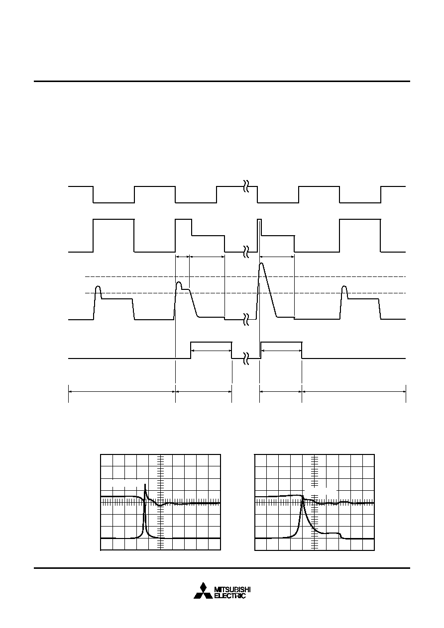
6.4.4 Over-Current Protection
The IPM uses current sense IGBT
chips to continuously monitor
power device current. If the current
though the Intelligent Power Mod-
ule exceeds the specified
overcurrent trip level (OC) for a pe-
riod longer than t
off(OC)
the IPMs
internal control circuit will protect
the power device by disabling the
gate drive and generating a fault
output signal. The timing of the
over-current protection is shown in
Figure 6.17. The t
off(OC)
delay is
implemented in order to avoid trip-
ping of the OC protection on short
pulses of current above the OC
level that are not dangerous for the
power device. When an over-cur-
rent is detected a controlled shut-
down is initiated and a fault output
is generated. The controlled shut-
down lowers the turn-off di/dt which
helps to control transient voltages
that can occur during
shut down from high fault currents.
Most Intelligent Modules use the
two step shutdown depicted in Fig-
ure 6.17. In the two step shutdown,
the gate voltage is reduced to an
intermediate voltage causing the
current through the device to drop
slowly to a low level. Then, about
5
µ
s later, the gate voltage is re-
duced to zero completing the shut
down. Some of the large six and
seven pack IPMs use an active
ramp of gate voltage to achieve the
desired reduction in turn off di/dt
under high fault currents. The oscil-
lographs in Figure 6.18 illustrate
Figure 6.15
Operation of Under-Voltage Lockout
INPUT
SIGNAL
BASE PLATE
TEMPERATURE
(Tb)
FAULT OUTPUT
CURRENT
(I
FO
)
INTERNAL
GATE
VOLTAGE
V
GE
OT
OT
r
Figure 6.16
Operation of Over-Temperature
INPUT
SIGNAL
CONTROL
SUPPLY
VOLTAGE
FAULT
OUTPUT
CURRENT
(I
FO
)
INTERNAL
GATE
VOLTAGE
V
GE
CONTROL SUPPLY ON
SHORT
GLITCH
IGNORED
POWER SUPPLY
FAULT AND
RECOVERY
CONTROL SUPPLY OFF
UV
r
UV
t
t
FO
t
dUV
t
FO
t
dUV
MITSUBISHI SEMICONDUCTORS POWER MODULES MOS
USING INTELLIGENT POWER MODULES
Sep.1998
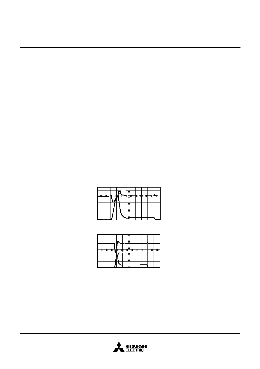
the effect of the controlled shut-
down (for obtaining the oscillo-
graph in "A"
the internal soft shutdown was in-
tentionally deactivated). The IPM
uses actual device current mea-
surement to detect all types of over
current conditions. Even resistive
and inductive shorts to ground that
are often missed by conventional
desaturation and bus current sens-
ing protection schemes will be de-
tected by the IPMs current sense
IGBTs.
Note:
V-Series IPMs do not have an
over- current protection function.
Instead a unified short circuit pro-
tection function that has a delay
like the over current protection de-
scribed in this section is used.
NORMAL OPERATION
FWD RECOVERY CURRENT
IGNORED BY OC PROTECTION
OVER CURRENT
FAULT AND
RECOVERY
SHORT CIRCUIT
FAULT AND
RECOVERY
NORMAL OPERATION
t
FO
t
FO
thold
thold
t
off
(OC)
INPUT
SIGNAL
INTERNAL
GATE
VOLTAGE
(V
GE
)
SHORT CIRCUIT
TRIP LEVEL
OVER CIRCUIT
TRIP LEVEL
COLLECTOR
CURRENT
I
FO
FAULT OUTPUT
CURRENT
Figure 6.17
Operation of Over-Current and Short-Circuit Protection
OC PROTECTION WITHOUT SOFT SHUTDOWN
V
CE (surge)
OC PROTECTION WITH SOFT SHUTDOWN
I
C
V
CE
I
C
V
CE
V
CE (surge)
Figure 6.18
OC Operation of PM200DSA060 (I
C
: 100A/div; 100V/div; t: 1
µ
s/div)
MITSUBISHI SEMICONDUCTORS POWER MODULES MOS
USING INTELLIGENT POWER MODULES
Sep.1998
6.4.5 Short Circuit Protection
If a load short circuit occurs or the
system controller malfunctions
causing a shoot through, the IPMs
built in short circuit protection will
prevent the IGBTs from being dam-
aged. When the current, through
the IGBT exceeds the short circuit
trip level (SC), an immediate con-
trolled shutdown is initiated and a
fault output is generated. The same
controlled shutdown techniques
used in the over current protection
are used to help control transient
voltages during short circuit shut
down. The short circuit protection
provided by the IPM uses actual
current measurement to detect
dangerous conditions. This type of
protection is faster and more reli-
able than conventional out-of-satu-
ration protection schemes. Figure
6.17 is a timing diagram showing
the operation of the short circuit
protection.
To reduce the response time be-
tween SC detection and SC shut-
down, a real time current control
circuit (RTC) has been adopted.
The RTC bypasses all but the final
stage of the IGBT driver in SC op-
eration thereby reducing the re-
sponse time to less than 100ns.
The oscillographs in Figure 6.19 il-
lustrate the effectiveness of the
RTC technique by comparing short
circuit operation of second genera-
tion IPM (without RTC) and third
generation IPM (with RTC).
A significant improvement can be
seen as the power stress is much
lower as the time in short circuit
and the magnitude of the short cir-
cuit current are substantially re-
duced.
Note:
The short circuit protection in
V-Series IPMs has a delay similar
to the third generation over current
protection function described in
6.4.4. The need for a quick trip has
been eliminated through the use of
a new advanced RTC circuit.
Caution:
1.
Tripping of the over current
and short circuit protection indi-
cates stressful operation of the
IGBT. Repetitive tripping must
be avoided.
2.
High surge voltages can occur
during emergency shutdown.
Low inductance buswork and
snubbers are recommended.
6.5 IPM Selection
There are two key areas that must
be coordinated for proper selection
of an IPM for a particular inverter
application. These are peak
current coordination to the IPM
overcurrent trip level and proper
thermal design to ensure that
peak junction temperature is al-
ways less than the maximum junc-
tion temperature rating
(150
∞
C) and that the baseplate
temperature remains below the
over-temperature trip level.
6.5.1 Coordination of OC Trip
Peak current is addressed by refer-
ence to the power rating of the mo-
tor. Tables 6.2, 6.3 and 6.4 give
recommended IPM types derived
from the OC trip level and the peak
motor current requirement based
on several assumptions for the in-
verter and motor operation regard-
ing efficiency, power factor, maxi-
mum overload, and current ripple.
For the purposes of this table, the
maximum motor current is taken
from the NEC table. This already
includes the motor efficiency and
power factor appropriate to the par-
ticular motor size. Peak inverter
current is then calculated using this
RMS current, a 200% overload re-
quirement, and a 20% ripple factor.
An IPM is then selected which has
a minimum overcurrent trip level
that is above this calculated peak
operating requirement.
Figure 6.19
Waveforms
Showing the Effect
of the RTC Circuit
SHORT CIRCUIT OPERATION WITHOUT RTC CIRCUIT
100A, 600V, IPM
SHORT CIRCUIT OPERATION WITH RTC CIRCUIT
100A, 600V, IPM
800A
V
CE
I
C
I
C
=200A/div,
V
CE
=100V/div, t=1µs/div
V
CE
T
I
C
T
410A
I
C
=200A/div,
V
CE
=100V/div, t=1µs/div
T
T
MITSUBISHI SEMICONDUCTORS POWER MODULES MOS
USING INTELLIGENT POWER MODULES

Sep.1998
Table 6.2 Motor Rating vs. OC Protection (230 VAC Line)
Current
Motor Rating (HP)
NEC Current Rating A(RMS)
Inverter Peak Current (A)*
Applicable IPM
Minimum OC Trip (A)
0.5
2.0
6.8
PM10CSJ060
12
0.75
2.8
9.5
PM10CSJ060
12
1
3.6
12.2
PM15CSJ060
18
1.5
5.2
17.6
PM15CSJ060
18
2
6.8
23
PM20CSJ060
28
3
9.6
32
PM30CSJ060, PM30RSF060
39
5
15.2
52
PM50RSA060, PM50RSK060
65
7.5
22
75
PM75RSA060, PM75RSK060
115
10
28
95
PM75RSA060, PM75RSK060
115
15
42
143
PM100CSA060, PM100RSA060
158
20
54
183
PM150CSA060, PM150RSA060
210
25
68
231
PM200CSA060, PM200RSA060,
310
PM200DSA060 x3
30
80
271
PM200CSA060, PM200RSA060,
310
PM200DSA060 x3
40
104
353
PM300DSA060 x3
390
50
130
441
PM400DSA060 x3
500
60
154
523
PM600DSA060 x3
740
75
192
652
PM600DSA060 x3
740
100
256
869
PM800HSA060 x6
1000
- From NEC Table 430-150
* - Inverter peak current is based on 200% overload requirement and a 20% current ripple factor.
Table 6.3 Motor Rating vs. OC Protection (460 VAC Line)
Current
Motor Rating (HP)
NEC Current Rating A(RMS)
Inverter Peak Current (A)*
Applicable IPM
Minimum OC Trip (A)
0.5
1.0
3.4
PM10RSH120, PM10CZF120
15
0.75
1.4
4.8
PM10RSH120, PM10CZF120
15
1
1.8
6.1
PM10RSH120, PM10CZF120
15
1.5
2.6
8.8
PM10RSH120, PM10CZF120
15
2
3.4
12
PM10RSH120, PM10CZF120
15
3
4.8
16
PM15RSH120, PM15CZF120
22
5
7.6
26
PM25RSB120, PM25RSK120
32
7.5
11
37
PM50RSA120
59
10
14
48
PM50RSA120
59
15
21
71
PM75CSA120, PM75DSA120 x3
105
20
27
92
PM75CSA120, PM75DSA120 x3
105
25
34
115
PM100CSA120, PM100DSA120 x3
145
30
40
136
PM100CSA120, PM100DSA120 x3
145
40
52
176
PM150DSA120 x3
200
50
65
221
PM200DSA120 x3
240
60
77
261
PM300DSA120 x3
380
75
96
326
PM300DSA120 x3
380
100
124
421
PM400HSA120 x6
480
125
156
529
PM600HSA120 x6
740
150
180
611
PM600HSA120 x6
740
200
240
815
PM800HSA120 x6
1060
250
300
1020
PM800HSA120 x6
1060
- From NEC Table 430-150
* - Inverter peak current is based on 200% overload requirement and a 20% current ripple factor.
MITSUBISHI SEMICONDUCTORS POWER MODULES MOS
USING INTELLIGENT POWER MODULES
Sep.1998
6.5.2 Estimating Losses
Once the coordination of the
OC trip with the application require-
ments has been established the
next step is determining the cooling
system requirements. Section 3.4
provides a general description of
the methodology for loss estimation
and thermal system design. Figure
6.20 shows the total switching en-
ergy (E
SW(on)
+E
SW(off)
) versus I
C
for all third generation IPMs.
Figure 6.21 shows total switching
energy versus I
C
for V-Series
IPMs. A detailed explanation of
these curves and their use can be
found in Section 3.4.1. Figures
6.22 through 6.34 show simulation
results calculating total power loss
(switching and conduction) per arm
in a sinusoidal output PWM inverter
application using V-Series IPMs.
Table 6.4 Motor Rating vs. SC Protection for V-Series IPMs
Current
Motor Rating (HP)
NEC Current Rating A(RMS)
Inverter Peak Current (A)*
Applicable IPM
Minimum SC Trip (A)
240VAC Line
10
28
95
PM75RVA060
115
15
42
143
PM100CVA060
158
20
54
183
PM150CVA060
210
30
80
271
PM200CVA060
310
40
104
353
PM300CVA060
396
50
130
441
PM400DVA060
650
75
192
652
PM600DVA060
1000
460VAC Line
10
14
48
PM50RVA120
59
20
27
92
PM75CVA120
105
30
40
136
PM100CVA120
145
40
52
176
PM150CVA120
200
50
65
221
PM200DVA120
240
75
96
326
PM300DVA120
380
- From NEC Table 430-150
* - Inverter peak current is based on 200% overload requirement and a 20% current ripple factor.
10
0
10
1
10
2
10
3
10
4
10
-1
10
0
COLLECTOR CURRENT, I
C
, (AMPERES)
SWITCHINTG DISSIPATION, (mJ/PULSE)
10
1
10
3
10
2
CONDITIONS:
INDUCTIVE LOAD
SWITCHING OPERATION
T
j
= 125
o
C
V
CC
= 1/2 V
CES
V
D
= 15V
SWITCHING DISSIPATION =
TURN-ON DISSIPATION +
TURN-OFF DISSIPATION
COMPATIBLE I
C
RANGE:
RATED I
C
◊
0.1 ~ 1.4
600V SERIES
1200V SERIES
APPLICABLE TYPES: THIRD-GENERATION IPM
PM200DSA060,
PM75DSA120,
PM300DSA120,
PM75CSA120,
PM20CSJ060,
PM50RSK060,
PM10RSH120,
PM300DSA060,
PM100DSA120,
PM100CSA060,
PM100CSA120,
PM300CSJ060,
PM75RSA060,
PM15RSH120,
PM400DSA060,
PM150DSA120,
PM150CSA060,
PM10CSJ060,
PM30RSF060,
PM100RSA060,
PM25RSB120,
PM600DSA060,
PM200DSA120,
PM200CSA060,
PM15CSJ060,
PM50RSA060,
PM150RSA060,
PM50RSA120
Figure 6.20
Switching Energy vs. I
C
for Third Generation IPMs
MITSUBISHI SEMICONDUCTORS POWER MODULES MOS
USING INTELLIGENT POWER MODULES
Sep.1998
10
0
10
1
10
2
10
3
10
4
10
-1
10
0
COLLECTOR CURRENT, I
C
, (AMPERES)
SWITCHING ENERGY LOSS
FOR V-SERIES IPMs
SWITCHING ENERGY, (mJ/PULSE)
10
1
10
3
10
2
CONDITIONS:
INDUCTIVE LOAD
T
j
= 125
o
C
V
CC
= 1/2 V
CES
V
D
= 15V
600V SERIES
1200V SERIES
E
SW (ON)
+ E
SW (OFF)
COMPATIBLE I
C
RANGE:
RATED I
C
◊
0.1 ~ 1.4
0
20
40
60
100
80
120
0
I
O
(ARMS)
50
P(W)
100
150
200
250
DC LOSS
SW LOSS
TOTAL LOSS
V
CC
= 300V
V
D
= 15V
T
j
= 125∞C
P.F. = 0.8
fc = 10kHz
Figure 6.21
Figure 6.22
Power Loss
Simulation of
PM75RVA060 (Typ.)
Figure 6.23
Power Loss
Simulation of
PM100CVA060 (Typ.)
Figure 6.24
Power Loss
Simulation of
PM150CVA060 (Typ.)
Figure 6.25
Power Loss
Simulation of
PM200CVA060 (Typ.)
Figure 6.27
Power Loss
Simulation of
PM400DVA060 (Typ.)
Figure 6.28
Power Loss
Simulation of
PM600DVA060 (Typ.)
Figure 6.26
Power Loss
Simulation of
PM300CVA060 (Typ.)
Figure 6.29
Power Loss
Simulation of
PM50RVA120 (Typ.)
0
20
40
60
100
80
120
0
I
O
(ARMS)
50
P(W)
100
150
200
250
DC LOSS
SW LOSS
TOTAL LOSS
V
CC
= 300V
V
D
= 15V
T
j
= 125∞C
P.F. = 0.8
fc = 10kHz
0
20
40
60
100
80
120
0
I
O
(ARMS)
50
P(W)
100
150
200
250
DC LOSS
SW LOSS
TOTAL LOSS
V
CC
= 300V
V
D
= 15V
T
j
= 125∞C
P.F. = 0.8
fc = 10kHz
0
40
80
120
200
160
240
0
I
O
(ARMS)
50
P(W)
100
150
200
250
DC LOSS
SW LOSS
TOTAL LOSS
V
CC
= 300V
V
D
= 15V
T
j
= 125∞C
P.F. = 0.8
fc = 10kHz
0
40
80
120
200
160
240
0
I
O
(ARMS)
50
P(W)
100
150
200
250
DC LOSS
SW LOSS
TOTAL LOSS
V
CC
= 300V
V
D
= 15V
T
j
= 125∞C
P.F. = 0.8
fc = 10kHz
0
40
80
120
200
160
240
0
I
O
(ARMS)
50
P(W)
100
150
200
250
DC LOSS
SW LOSS
TOTAL LOSS
V
CC
= 300V
V
D
= 15V
T
j
= 125∞C
P.F. = 0.8
fc = 10kHz
0
40
80 120
200
160
360
320
240 280
0
I
O
(ARMS)
50
P(W)
100
150
300
250
200
350
DC LOSS
SW LOSS
TOTAL LOSS
V
CC
= 300V
V
D
= 15V
T
j
= 125∞C
P.F. = 0.8
fc = 10kHz
0
15
30
45
90
75
60
0
I
O
(ARMS)
50
P(W)
100
150
300
250
200
350
DC LOSS
SW LOSS
TOTAL LOSS
V
CC
= 600V
V
D
= 15V
T
j
= 125∞C
P.F. = 0.8
fc = 10kHz
MITSUBISHI SEMICONDUCTORS POWER MODULES MOS
USING INTELLIGENT POWER MODULES
Sep.1998
6.6
Controlling the Intelligent
Power Module
IPM (Intelligent Power Modules)
are easy to operate. The integrated
drive and protection circuits require
only an isolated power supply and
a low level on/off control signal. A
fault output is provided for monitor-
ing the operation of the modules in-
ternal protection circuits.
6.6.1 The Control Power Supply
Depending on the power circuit
configuration of the module one,
two, or four isolated power supplies
are required by the IPMs internal
drive and protection circuits. In high
power 3-phase inverters using
single or dual type IPMs it is good
practice to use six isolated power
supplies. In these high current ap-
plications each low side device
must have its own isolated control
power supply in order to avoid
ground loop noise problems. The
control supplies should be regu-
lated to 15V +/-10% in order to
avoid over-voltage damage or false
tripping of the under-voltage pro-
tection. The supplies should have
an isolation voltage rating of at
least two times the IPM's V
CES
rat-
ing (i.e. V
iso
= 2400V for 1200V
module). The current that must be
supplied by the control power sup-
ply is the sum of the quiescent cur-
rent needed to power the internal
control circuits and the current re-
quired to drive the IGBT gate.
Table 6.5 summarizes the typical
and maximum control power
supply current requirements for
Figure 6.30
Power Loss
Simulation of
PM75RVA1200 (Typ.)
Figure 6.31
Power Loss
Simulation of
PM100CVA120 (Typ.)
Figure 6.33
Power Loss
Simulation of
PM200DVA120 (Typ.)
Figure 6.34
Power Loss
Simulation of
PM300DVA120 (Typ.)
Figure 6.32
Power Loss
Simulation of
PM150CVA120 (Typ.)
0
15
30
45
90
75
60
0
I
O
(ARMS)
50
P(W)
100
150
300
250
200
350
DC LOSS
SW LOSS
TOTAL LOSS
V
CC
= 600V
V
D
= 15V
T
j
= 125∞C
P.F. = 0.8
fc = 10kHz
0
20
40 60
100
80
180
160
120 140
0
I
O
(ARMS)
50
P(W)
100
150
300
250
200
350
DC LOSS
SW LOSS
TOTAL LOSS
V
CC
= 600V
V
D
= 15V
T
j
= 125∞C
P.F. = 0.8
fc = 10kHz
0
20
40 60
100
80
180
160
120 140
0
I
O
(ARMS)
50
P(W)
100
150
300
250
200
350
DC LOSS
SW LOSS
TOTAL LOSS
V
CC
= 600V
V
D
= 15V
T
j
= 125∞C
P.F. = 0.8
fc = 10kHz
0
20
40 60
100
80
180
160
120 140
0
I
O
(ARMS)
50
P(W)
100
150
300
250
200
350
DC LOSS
SW LOSS
TOTAL
LOSS
V
CC
= 600V
V
D
= 15V
T
j
= 125∞C
P.F. = 0.8
fc = 10kHz
0
20
40 60
100
80
180
160
120 140
0
I
O
(ARMS)
50
P(W)
100
150
300
250
200
350
DC LOSS
SW LOSS
TOTAL
LOSS
V
CC
= 600V
V
D
= 15V
T
j
= 125∞C
P.F. = 0.8
fc = 10kHz
MITSUBISHI SEMICONDUCTORS POWER MODULES MOS
USING INTELLIGENT POWER MODULES

Sep.1998
third generation Intelligent Power
Modules. Table 6.6 summarizes
control supply requirements for
V-Series IPMs. These tables give
control circuit currents for the qui-
escent (not switching) state and for
20kHz switching. This data is pro-
vided in order to help the user de-
sign appropriately sized control
power supplies.
Power requirements for operating
frequencies other than 20kHz can
be determined by scaling the fre-
quency dependent portion of the
control circuit current. For example,
to determine the maximum control
circuit current for a PM300DSA120
operating at 7kHz the maximum
quiescent control circuit current is
subtracted from the maximum
20kHz control circuit current:
70mA ≠ 30mA = 40mA
40mA is the frequency dependent
portion of the control circuit current
for 20kHz operation. For 7kHz
operation the frequency
dependent portion is:
40mA x (7kHz
˜
20kHz) = 14mA
To get the total control power sup-
ply current required, the quiescent
current must be added back:
30mA + 14mA = 44mA
44mA is the maximum control cir-
cuit current required for a
PM300DSA120 operating at 7kHz.
Capacitive coupling between pri-
mary and secondary sides
of isolated control supplies must
be minimized as parasitic capaci-
tances in excess of 100pF can
cause noise that may trigger
Table 6.5 Control Power Requirements for Third Generation IPMs
(V
D
= 15V, Duty = 50%) ma
N Side
P Side (Each Supply)
DC
20kHz
DC
20kHz
Type Name
Typ.
Max
Typ.
Max.
Typ.
Max.
Typ.
Max.
600V Series
PM10CSJ060
18
25
23
32
7
10
8
12
PM15CSJ060
18
25
23
32
7
10
8
12
PM20CSJ060
18
25
24
34
7
10
8
12
PM30CSJ060
18
25
24
34
7
10
9
13
PM100CSA060
40
55
78
100
13
18
25
34
PM150CSA060
40
55
80
110
13
18
25
38
PM200CSA060
40
55
85
120
13
18
27
40
PM30RSF060
25
30
32
45
7
10
9
13
PM50RSA060
44
60
70
100
13
18
23
32
PM50RSK060
44
60
70
100
13
18
23
32
PM75RSA060
44
60
75
100
13
18
24
35
PM100RSA060
44
60
78
105
13
18
25
36
PM150RSA060
52
72
72
113
13
18
26
38
PM200RSA060
52
72
85
115
13
18
26
40
PM200DSA060
19
26
30
42
19
26
30
42
PM300DSA060
19
26
35
48
19
26
35
48
PM400DSA060
23
30
40
60
23
30
40
60
PM600DSA060
23
30
50
70
23
30
50
70
PM800HSA060
23
30
50
70
≠
≠
≠
≠
1200V SERIES
PM10RSH120
25
35
31
44
7
10
9
13
PM10CZF120
18
25
7
10
9
13
PM15RSH120
25
35
32
45
7
10
9
13
PM15CZF120
18
25
7
10
9
13
PM25RSB120
44
60
60
83
13
18
18
25
PM25RSK120
44
60
60
83
13
18
18
25
PM50RSA120
44
60
65
90
13
18
19
27
PM75CSA120
44
60
60
83
13
18
20
28
PM100CSA120
40
55
75
104
13
18
25
35
PM75DSA120
13
20
20
28
13
20
20
28
PM100DSA120
19
26
30
42
19
26
30
42
PM150DSA120
19
26
35
48
19
26
35
48
PM200DSA120
23
30
48
67
23
30
48
67
PM300DSA120
23
30
50
70
23
30
50
70
PM400HSA120
23
30
60
90
≠
≠
≠
≠
PM600JSA120
23
30
60
90
≠
≠
≠
≠
PM800HSA120
30
40
≠
≠
≠
≠
≠
≠
MITSUBISHI SEMICONDUCTORS POWER MODULES MOS
USING INTELLIGENT POWER MODULES

Sep.1998
the control circuits. An electrolytic
or tantalum decoupling capacitor
should be connected across the
control power supply at the IPMs
terminals. This capacitor will help
to filter common noise on the con-
trol power supply and provide the
high pulse currents required by the
IPMs internal gate drive circuits.
Isolated control power supplies can
be created using a variety of tech-
niques. Control power can be de-
rived from the main input line using
either a switching power supply
with multiple outputs or a line fre-
quency transformer with multiple
secondaries. Control power sup-
plies can also be derived from the
main logic power supply using DC-
to-DC converters. Using a compact
DC-to-DC converter for each iso-
lated supply can help to simplify
the interface circuit layout. A distrib-
uted DC-to-DC converter in which
a single oscillator is used to drive
several small isolation transformers
can provide the layout advantages
of separate DC-to-DC converters at
a lower cost.
In order to simplify the design of
the required isolated power sup-
plies, Mitsubishi has developed two
DC-to-DC converter modules to
work with the IPMs. The M57120L
is a high input voltage step down
converter. When supplied with 113
to 400VDC the M57120L will pro-
duce a regulated 20VDC output.
The 20VDC can then be connected
to the M57140-01 to produce four
isolated 15VDC outputs to power
the IPMs control circuits. The
M57140-01 can also be used as a
stand alone unit if 20VDC is avail-
able from another source such as
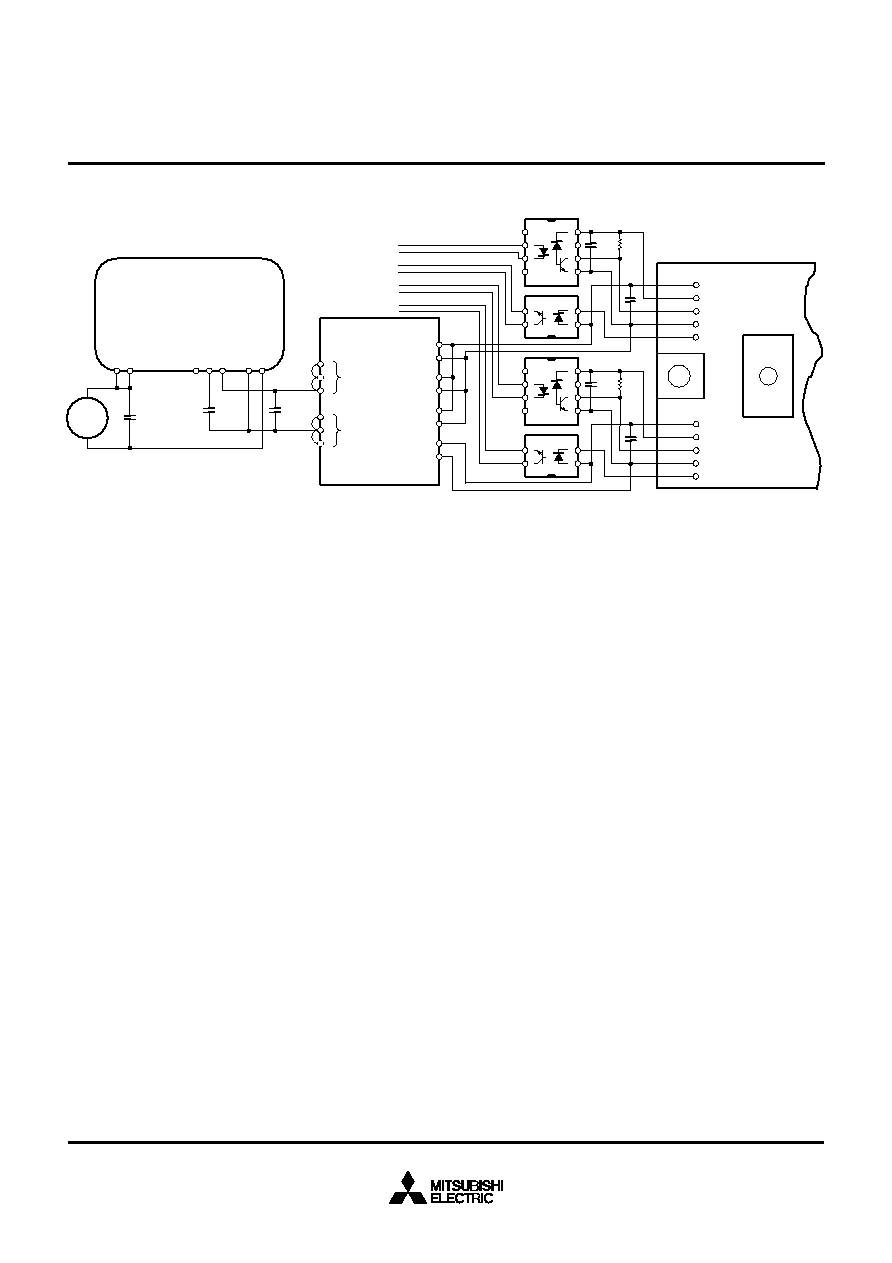
the main logic power supply. Figure
6.35 shows an isolated interface
circuit for a seven pack IPM using
M57140-01. Figure 6.36 shows a
complete high input voltage iso-
lated power supply circuit for a dual
type intelligent power module.
Caution:
Using bootstrap techniques is not
recommended because the voltage
ripple on VD may cause a false trip
of the undervoltage protection in
certain inverter PWM modes.
6.6.2 Interface Circuit Require-
ments
The IGBT power switches in the
IPM are controlled by a low level
input signal. The active low control
input will keep the power devices
off when it is held high. Typically
the input pin of the IPM is pulled
high with a resistor connected to
the positive side of the control
power supply. An ON signal is then
generated by pulling the control in-
put low. The fault output is an open
collector with its maximum sink cur-
rent internally limited. When a fault
condition occurs the open collector
device turns on allowing the fault
output to sink current from the posi-
tive side of the control supply. Fault
and on/off control signals are usu-
ally transferred to and from the sys-
tem controller using isolating inter-
face circuits. Isolating interfaces al-
low high and low side control sig-
nals to be referenced to a common
logic level. The isolation is usually
provided by optocouplers. How-
ever, fiber optics, pulse transform-
ers, or level shifting circuits could
be used. The most important con-
sideration in interface circuit design
is layout. Shielding and careful
routing of printed circuit wiring is
necessary in order to avoid cou-
pling of dv/dt noise into control cir-
cuits. Parasitic capacitance be-
tween high side
Table 6.6 V-Series IPM Control Power Supply Current
N Side
P Side (Each Supply)
DC
20kHz
DC
20kHz
Type Name
Typ.
Max
Typ.
Max.
Typ.
Max.
Typ.
Max.
600V Series
PM75RVA060
44
60
72
94
13
18
21
27
PM100CVA060
40
55
68
88
13
18
22
29
PM150CVA060
40
55
72
94
13
18
23
30
PM200CVA060
40
55
84
110
13
18
28
36
PM300CVA060
52
72
130
170
17
24
43
56
PM400DVA060
23
30
56
73
23
30
56
73
PM600DVA060
23
30
56
73
23
30
56
73
1200V SERIES
PM50RVA120
44
60
73
95
13
18
21
27
PM75CVA120
40
55
70
92
13
18
24
31
PM100CVA120
40
55
80
104
13
18
26
34
PM150CVA120
72
100
128
166
24
34
42
55
PM200DVA120
37
48
52
68
37
48
52
68
PM300DVA120
37
48
52
68
37
48
52
68
MITSUBISHI SEMICONDUCTORS POWER MODULES MOS
USING INTELLIGENT POWER MODULES
Sep.1998
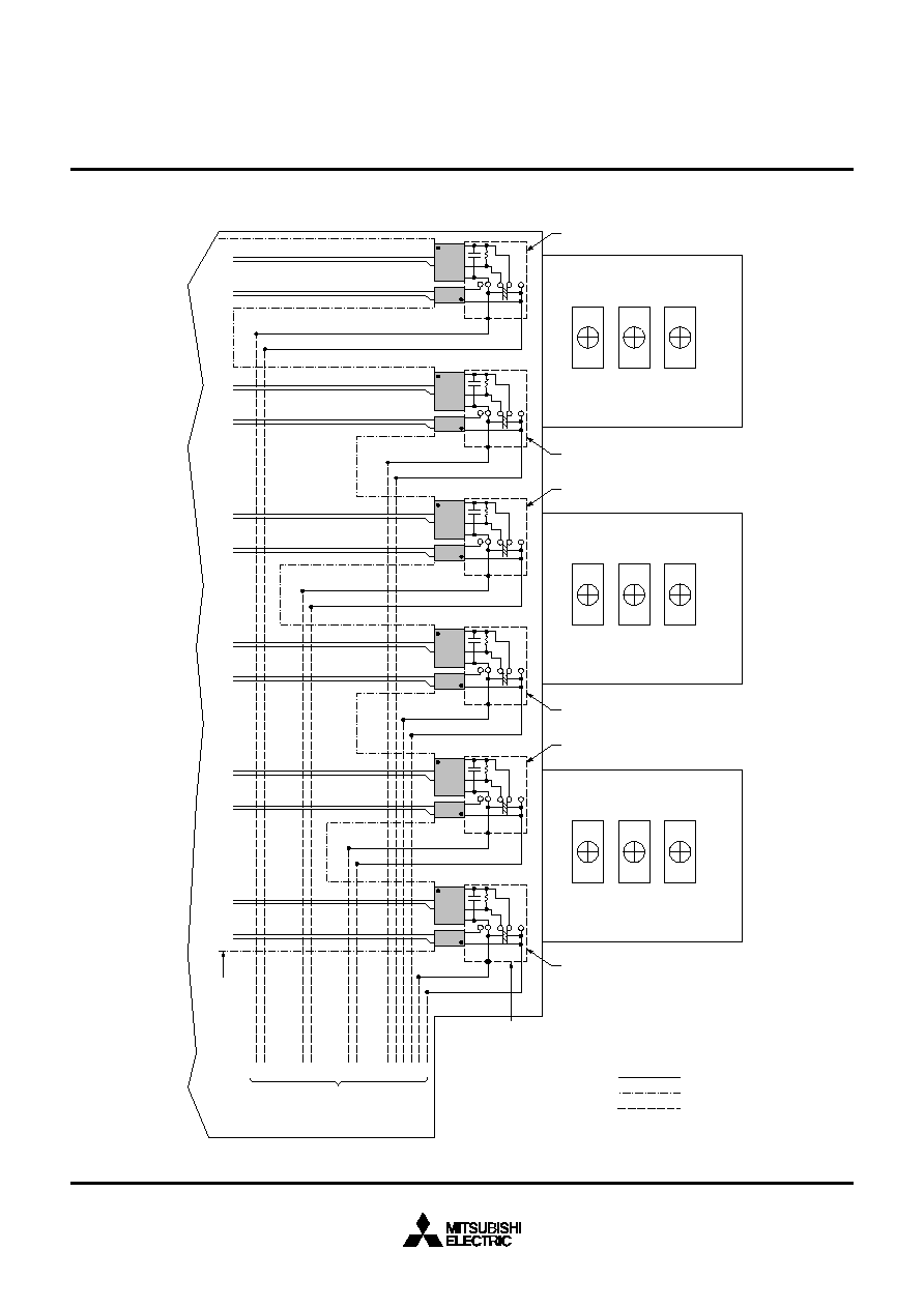
1
HCPL4504
0.1
µ
F
SEVEN PACK IPM
V
UP1
U
P
V
UPC
U
FO
C
1
20k
0.1
µ
F
20k
2
3
4
8
7
6
5
3
PC817
4
2
1
1
HCPL4504
2
3
4
8
7
6
5
3
PC817
4
1
2
3
4
5
-
+
+
6
7
8
9
10
11
VIN
12
13
14
0
+15
0
+15
0
+15
0
+15
2
1
4
3
2
1
V
VP1
V
P
V
VPC
V
FO
V
WP1
W
P
V
WPC
W
FO
U
N
B
R
V
NC
V
NI
F
O
V
N
W
N
8
7
6
5
12
11
10
9
16
15
14
13
19
18
17
1
HCPL4504
0.1
µ
F
+
+
20k
2
3
4
8
7
6
5
3
PC817
4
2
1
C
1
+
C
1
+
1
HCPL4504
0.1
µ
F
4.7k
C
2
+
2
3
4
8
7
6
5
1
PC817
2
4
3
1
HCPL4504
0.1
µ
F
2
3
4
8
7
6
5
1
HCPL4504
0.1
µ
F
20k
20k
20k
2
3
4
8
7
6
5
3
PC817
4
2
1
20V
330
µ
F
FO
N
W
N
V
N
U
N
B
W
P
FO
WP
V
P
FO
VP
U
P
FO
UP
NOTE: FOR C1 AND C2 SEE SECTION 6.6.3
Figure 6.35
Isolated Interface Circuit for Seven-Pack IPMs
MITSUBISHI SEMICONDUCTORS POWER MODULES MOS
USING INTELLIGENT POWER MODULES
Sep.1998
interface circuits, high and low side
interface circuits, or primary and
secondary sides of the isolating de-
vices can cause noise problems.
Careful layout of control power
supply and isolating circuit wiring is
necessary. The following is a list of
guidelines that should be followed
when designing interface circuits.
Figure 6.37 shows an example in-
terface circuit layout for dual type
IPMs. Figure 6.38 shows an ex-
ample interface circuit layout for a
V-Series IPMs.The shielding and
printed circuit routing techniques
used in this example are intended
to illustrate a typical application of
the layout guidelines.
INTERFACE CIRCUIT
LAYOUT GUIDELINES
I.
Maintain maximum interface
isolation. Avoid routing printed
circuit board traces from pri-
mary and secondary sides of
the isolation device near to or
above and below each other.
Any layout that increases the
primary to secondary capaci-
tance of the isolating interface
can cause noise problems.
II.
Maintain maximum control
power supply isolation. Avoid
routing printed circuit board
traces from UP, VP, WP, and N
side supplies near to each
other. High dv/dts exist be-
tween these supplies and
noise will be coupled through
parasitic capacitances.
If isolated power supplies are
derived from a common trans-
former interwinding capaci-
tance should be minimized.
III. Keep printed circuit board
traces between the interface
circuit and IPM short. Long
traces have a tendency to pick
up noise from other parts of the
circuit.
IV. Use recommended decoupling
capacitors for power supplies
and optocouplers. Fast switch-
ing IGBT power circuits gener-
ate dv/dt and di/dt noise. Every
precaution should be taken to
protect the control circuits from
coupled noise.
V.
Use shielding. Printed circuit
board shield layers are helpful
for controlling coupled dv/dt
noise. Figure 6.37 shows an
example of how the primary
and secondary sides of the iso-
lating interface can be
shielded.
VI. High speed optocouplers with
high common mode rejection
(CMR) should be used for sig-
nal input:
t
PLH
,t
PHL
< 0.8
µ
s
CMR > 10kV/
µ
s
@ V
CM
= 1500V
Appropriate optocoupler types
are HCPL 4503, HCPL 4504
(Hewlett Packard) and PS2041
(NEC). Usually high speed
optos require a 0.1
µ
F
decoupling capacitor close to
the opto.
VII. Select the control input pull-up
resistor with a low enough
value to avoid noise pick-up by
the high impedance IPM input
and with a high enough value
that the high speed
optotransistor can still pull the
IPM safely below the recom-
mended maximum V
CIN(on)
.
Figure 6.36
Isolated Interface Circuit for Dual Intelligent Power Modules
1
HCPL4504
0.1
µ
F
C
1
V
1
(+)
P
S
R
(+5)
C
IN
F
O
V
C (-)
V
1
(+)
N
C1
DUAL IPM
S
R
(+5)
C
IN
C
I
F
O
V
C (-)
+
6.8k
0.1
µ
F
6.8k
2
3
4
8
7
6
5
3
PC817
4
2
1
1
HCPL4504
2
3
4
8
7
6
5
3
PC817
4
3
2
2.2
µ
F
47
µ
F
50V
330
µ
F
50V
1
7
5
2 1
12
113-400
VDC
11
6
5
-
+
+
+
+
+
+
4
14
N
FO
N
IN
P
FO
P
IN
13
12
11
10
VIN
9
8
7
+15
0
+15
0
+15
0
+15
0
2
1
M57120L
1
2
3
4
5
1
2
3
4
5
MITSUBISHI SEMICONDUCTORS POWER MODULES MOS
USING INTELLIGENT POWER MODULES
Sep.1998
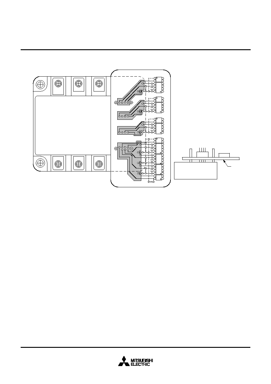
Figure 6.37
Interface Circuit Layout Example for Dual IPMs
W
N
V
N
U
N
W
P
V
P
U
P
+
-
+
-
+
-
+
-
+
-
+
-
F
O
W
N
F
O
W
P
F
O
V
N
V
P
F
O
U
N
F
O
U
P
F
O
SHIELDS GROUND
TO NEGATIVE SIDE
OF EACH CONTROL
POWER SUPPLY
DIGITAL
GROUND
MID-LAYER
SHIELD
TO
CONTROL
POWER
SOURCE
W
V
U
LEGEND
TOP LAYER
MIDDLE LAYER
BOTTOM LAYER
SHIELD GROUND TO V
UNC
SHIELD GROUND TO V
UPC
SHIELD GROUND TO V
VNC
SHIELD GROUND TO V
VPC
SHIELD GROUND TO V
WNC
SHIELD GROUND TO V
WPC
MITSUBISHI SEMICONDUCTORS POWER MODULES MOS
USING INTELLIGENT POWER MODULES
Sep.1998
VIII.If some IPM switches are not
used in actual application their
control power supply must still
be applied. The related signal
input terminals should be
pulled up by resistors to the
control power supply (V
D
or
V
SXR
) to keep the unused
switches safely in off-state.
IX. Unused fault outputs must be
tied high in order to avoid noise
pick up and unwanted activa-
tion of internal protection cir-
cuits. Unused fault outputs
should be connected directly to
the +15V of local isolated con-
trol power supply.
6.6.3 Example Interface Circuits
IPM (Intelligent Power Modules)
are designed to use optocoupled
transistors for control input and
fault output interfaces. In most ap-
plications optocouplers will provide
a simple and inexpensive isolated
interface to the system controller.
Figures 6.39 through 6.43 show ex-
ample interface circuits for the four
IPM power circuit configurations.
These circuits use two types of
optocoupled transistors. The con-
trol input on/off signals are trans-
ferred from the system controller
using high speed optocoupled tran-
sistors. Usually high speed optos
require a 0.1
µ
F film or ceramic
decoupling capacitor connected
near their V
CC
and GND pins. The
value of the control input pull up re-
sistor is selected low enough to
avoid noise pick up by the high im-
pedance input and high enough so
that the high speed optotransistor
with its relatively low current trans-
fer ratio can still pull the input low
enough to assure turn on. The cir-
cuits shown use a Hewlett Packard
HCPL-4504 optotransistor. This
opto was chosen mainly for its high
common mode transient immunity
of 15,000V/
µ
s. For reliable opera-
tion in IGBT power circuits
optocouplers should have a mini-
mum common mode noise immu-
nity of 10,000 V/
µ
s. Low speed
optocoupled transistors can be
used for the fault output and brake
input. Slow optos have the added
advantages of lower cost and
higher current transfer ratios. The
example interface circuits use a
Sharp PC817 low speed
optocoupled transistor for the
transfer of brake and fault signals.
Like most low speed optos the
PC817 does not have internal
shielding. Some switching noise
will be coupled through the opto.
An RC filter with a time constant of
about 10ms can be added to the
opto's output to remove this noise.
The IPMs 1.5ms long fault output
signal will be almost unaffected by
the addition of this filter. When de-
signing interface circuits always fol-
low the interface circuit layout
guidelines given in Section 6.6.2.
Figure 6.38
Interface Circuit Layout for a V-Series IPMs
B
P
N
U
V
W
IPM
IPM
INTERFACE CIRCUIT
PCB
MITSUBISHI SEMICONDUCTORS POWER MODULES MOS
USING INTELLIGENT POWER MODULES
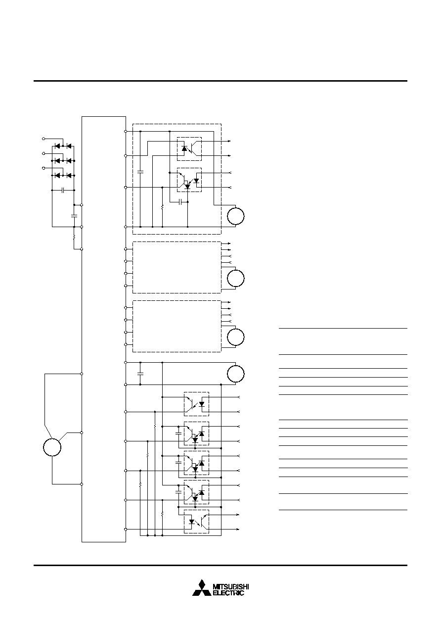
Sep.1998
Figure 6.39
Interface Circuit for Seven-Pack IPMs
N
P
B
U
V
W
LINE
MOTOR
+
C
S
V
UPC
UF
O
U
P
V
UP1
V
VPC
VF
O
V
P
V
VP1
V
WPC
WF
O
W
P
V
WP1
V
NC
V
N1
B
R
U
N
V
N
W
N
F
O
7-PACK THIRD GENERATION IPM
10
µ
F
20k
0.1
µ
F
15 V
+
FAULT
U
P
INTERFACE
INPUT
15 V
+
15 V
+
15 V
+
V
P
INTERFACE
W
P
INTERFACE
N SIDE INTERFACE
FAULT
OUTPUT
INPUT
BRAKE
U
N
INPUT
V
N
INPUT
W
N
INPUT
FAULT
0.1
µ
F
0.1
µ
F
0.1
µ
F
33
µ
F
20k
4.7k
20k
20k
SAME AS
U
P
INTERFACE
CIRCUIT
SAME AS
U
P
INTERFACE
CIRCUIT
FAULT
OUTPUT
INPUT
Rated
Decoupling
Applicable
Current
Capacitor
Types
(Amps)
(C
S
)
600V Modules
PM30RSF060
30
0.3
µ
F
PM50RSK060
55
0.47
µ
F
PM50RSA060
50
0.47
µ
F
PM75RSA060,
75
1.0
µ
F
PM75RSK060,
PM75RVA060
PM100RSA060
100
1.0
µ
F
PM150RSA060
150
1.5
µ
F
PM200RSA060
200
2.0
µ
F
1200V Modules
PM10RSH120
10
0.1
µ
F
PM15RSH120
15
0.1
µ
F
PM25RSB120,
25
0.22
µ
F
PM25RSK120
PM50RSA120,
50
0.47
µ
F
PM50RVA120
NOTE: If high side fault outputs are not used, they
must be connected to the +15V of the local power
supply.
MITSUBISHI SEMICONDUCTORS POWER MODULES MOS
USING INTELLIGENT POWER MODULES
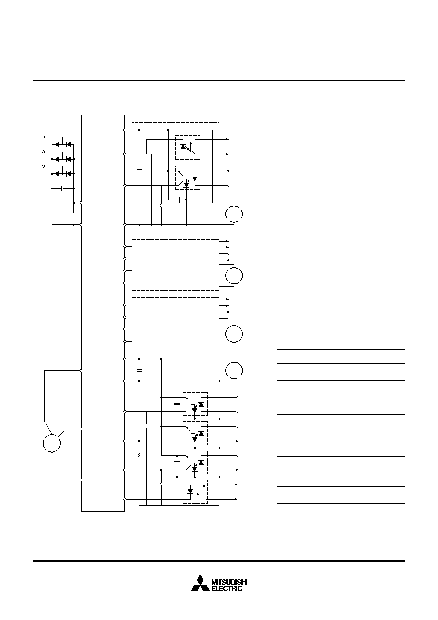
Sep.1998
Figure 6.40
Interface Circuit for Six-Pack IPMs
N
P
U
V
W
LINE
MOTOR
+
C
S
V
UPC
UF
O
U
P
V
UP1
V
WPC
VF
O
V
P
V
VP1
WF
O
V
WP1
V
NC
V
N1
U
N
V
N
W
N
F
O
6-PACK THIRD GENERATION IPM
10
µ
F
20k
0.1
µ
F
15 V
+
FAULT
U
P
INTERFACE
INPUT
15 V
+
15 V
+
15 V
+
V
P
INTERFACE
W
P
INTERFACE
N SIDE INTERFACE
FAULT
OUTPUT
INPUT
U
N
INPUT
V
N
INPUT
W
N
INPUT
FAULT
0.1
µ
F
0.1
µ
F
0.1
µ
F
33
µ
F
20k
20k
20k
SAME AS
U
P
INTERFACE
CIRCUIT
V
WPC
W
P
SAME AS
U
P
INTERFACE
CIRCUIT
FAULT
OUTPUT
INPUT
Rated
Decoupling
Applicable
Current
Capacitor
Types
(Amps)
(C
S
)
600V Modules
PM10CSJ060
10
0.1
µ
F
PM15CSJ060
15
0.1
µ
F
PM20CSJ060
20
0.1
µ
F
PM30CSJ060
30
0.3
µ
F
PM100CSA060,
100
1.0
µ
F
PM100CVA060
PM150CSA060,
150
1.5
µ
F
PM150CVA060
PM200CSA060,
200
2.2
µ
F
PM200CVA060
PM300CVA060
300
3.0
µ
F
1200V Modules
PM75CSA120,
75
1.0
µ
F
PM75CVA120
PM100CSA120,
100
1.0
µ
F
PM100CVA120
PM150CVA120
150
1.5
µ
F
NOTE: Unused fault outputs must be connected to
the +15V of the local control supply.
MITSUBISHI SEMICONDUCTORS POWER MODULES MOS
USING INTELLIGENT POWER MODULES

Sep.1998
Figure 6.41
Interface Circuit for Dual IPMs
C
2
6.8k
+
C
2
C
2
15 V
15 V
15 V
15 V
15 V
V
CC
W
V
U
MOTOR
IPM
+
+
+
+
+
IPM
IPM
INPUT
FAULT
+
+
0.1
µ
F
0.1
µ
F
6.8k
C
1
+
C
1
+
15 V
F
NO
V
NC
C
NI
S
NR
V
N1
F
PO
V
PC
C
PI
S
PR
V
P1
F
NO
V
NC
C
NI
S
NR
V
N1
F
PO
V
PC
C
PI
S
PR
V
P1
F
NO
V
NC
C
NI
S
NR
V
N1
F
PO
V
PC
C
PI
S
PR
V
P1
E
1
C
2
C
1
E
2
E
1
C
2
C
1
E
2
E
1
C
2
C
1
E
2
INPUT
FAULT
Control Power
Rated
Decoupling
Snubber
Applicable
Current
Capacitor
Capacitor
Types
(Amps)
(C
1
)
(C
2
)
600V Modules
PM200DSA060
200
47
µ
F
2.0
µ
F
PM300DSA060
300
47
µ
F
3.0
µ
F
PM400DSA060,
400
68
µ
F
4.0
µ
F
PM400DVA060
PM600DSA060,
600
68
µ
F
6.0
µ
F*
PM600DVA060
1200V Modules
PM75DSA120
75
22
µ
F
0.68
µ
F
PM100DSA120
100
47
µ
F
1.5
µ
F
PM150DSA120
150
47
µ
F
2.0
µ
F
PM200DSA120,
200
68
µ
F
3.0
µ
F
PM200DVA120
PM300DSA120,
300
68
µ
F
5.0
µ
F
PM300DVA120
*Depending on maximum DC link voltage and
main circuit layout, an RCDi clamp may be
needed. (see Section 3.3)
MITSUBISHI SEMICONDUCTORS POWER MODULES MOS
USING INTELLIGENT POWER MODULES
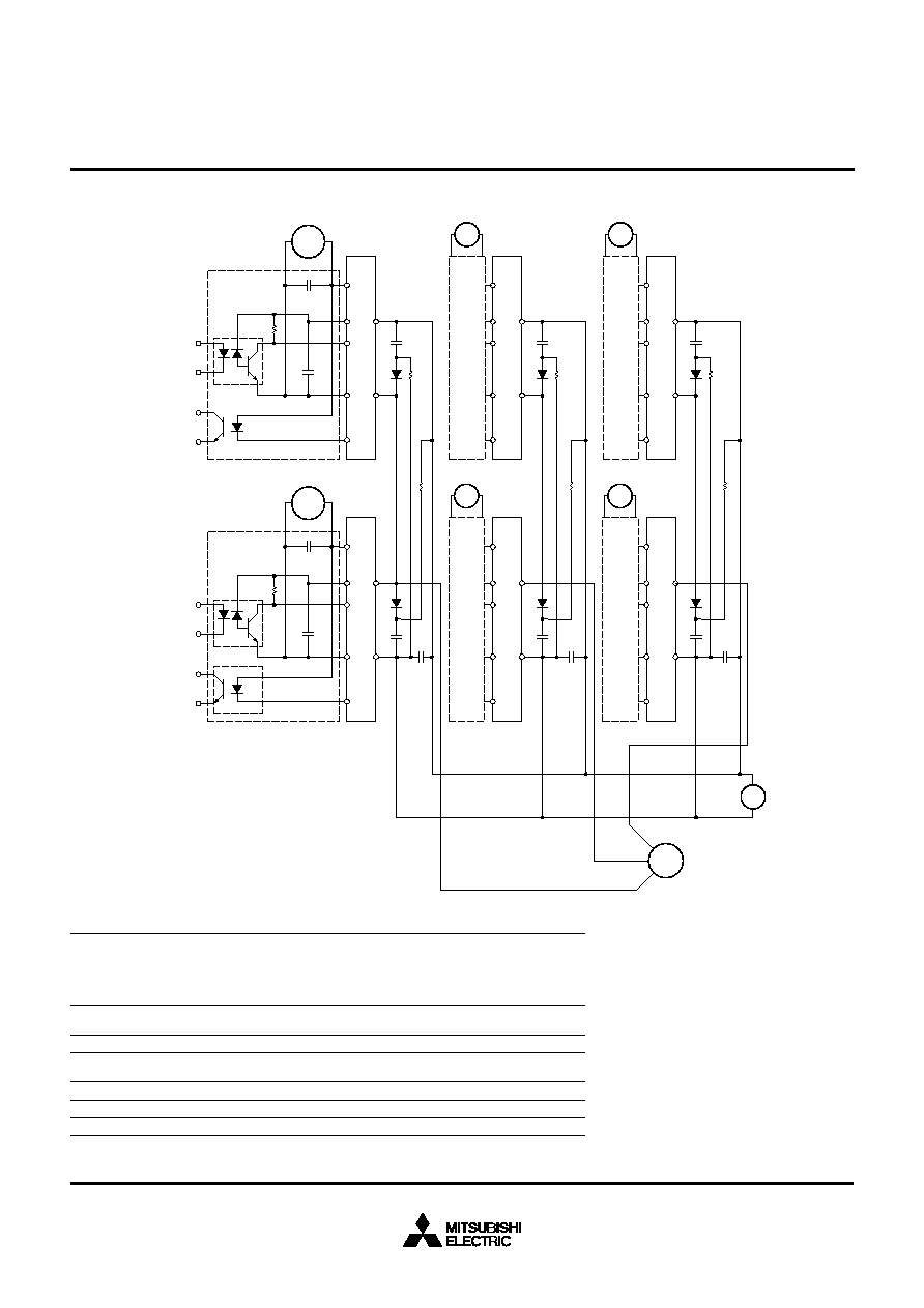
Sep.1998
Control Power
Main Bus
Rated
Decoupling
Snubber Decoupling
Applicable
Current
Capacitor
Capacitor Capacitor
Types
(Amps)
(C
1
)
(C
2
)
(C
3
)
Snubber Diode
600V Modules
PM800HSA060
800
68
µ
F
3.0
µ
F
6.0
µ
F
RM50HG-12S (2 pc. parallel)
1200V Modules
PM400HSA120
400
68
µ
F
1.5
µ
F
4.0
µ
F
RM25HG-24S
PM600HSA120
600
68
µ
F
2.0
µ
F
6.0
µ
F
RM25HG -24S (2 pc. parallel)
PM800HSA120
800
68
µ
F
3.0
µ
F
6.0
µ
F
RM25HG-24S (3 pc. parallel)
Figure 6.42
Interface Circuit for Single IPMs
+
+
15 V
6.8k
IPM
0.1
µ
F
C
1
INPUT
FAULT
V
1
S
R
C
1
C
2
V
C
C
E
D
F
O
+
+
15 V
6.8k
IPM
0.1
µ
F
C
1
V
1
S
R
C
1
V
C
C
E
F
O
C
2
C
3
C
3
C
3
D
IPM
V
1
S
R
C
1
C
2
V
C
C
E
D
F
O
IPM
V
1
S
R
C
1
V
C
C
E
F
O
C
2
D
IPM
V
1
S
R
C
1
C
2
V
C
C
E
D
F
O
IPM
V
1
S
R
C
1
V
C
C
E
F
O
C
2
D
+
+
+
15V
+
V
CC
+
MOTOR
U
V
W
INPUT
FAULT
15V
15V
15V
MITSUBISHI SEMICONDUCTORS POWER MODULES MOS
USING INTELLIGENT POWER MODULES
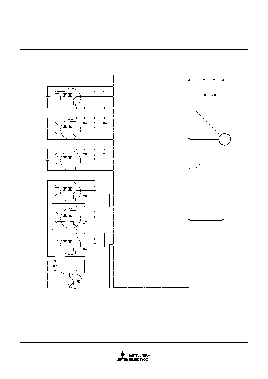
Sep.1998
Figure 6.43
Interface Circuit for PM10CZF120 and PM15CZF120
0.1
µ
0.1
µ
10
µ
+
≠
20k
20k
V
WP
W
P
V
WPC
U
N
V
N
W
N
V
N1
F
O
V
NC
I
F
V
D3
V
D3
V
D4
5V
10k
0.1
µ
10
µ
+
≠
20k
V
VP
V
P
V
VPC
I
F
V
D2
0.1
µ
10
µ
+
≠
20k
V
UP
U
P
V
UPC
I
F
V
D1
I
F
0.1
µ
20k
I
F
0.1
µ
20k
I
F
33
µ
+
≠
M
C
S
P
U
V
W
N
+
≠
V
CC
MITSUBISHI SEMICONDUCTORS POWER MODULES MOS
USING INTELLIGENT POWER MODULES
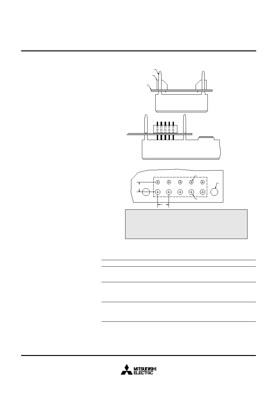
Sep.1998
6.6.4 Connecting the
Interface Circuit
The input pins of Mitsubishi Intelli-
gent Power Modules are designed
to be connected directly to a
printed circuit board. Noise pick up
can be minimized by building the
interface circuit on the PCB near
the input pins of the module. Low
power modules have tin plated
control and power pins that are de-
signed to be soldered directly to
the PCB. Higher power modules
have gold plated pins that are de-
signed to be connected to the PCB
using an inverse mounted header
receptacle. An example of this con-
nection for a dual type IPM is
shown in Figure 6.44. This connec-
tion technique can also be adapted
to large six and seven pack mod-
ules. Table 6.7 shows the sug-
gested connection method and
connector for each Third Genera-
tion IPM.
Table 6.8 shows the suggested
connection method and connector
for V-Series IPMs. Figure 6.45
shows the PCB layout for V-Series
six and seven pack connector.
Figure 6.44
Connection of the Interface Circuit
A
B
C
D
E
Hole for Header receptacle pin
Clearance Hole for IPM pin
Clearance Hole for IPM guide pin
IPM pin spacing
Header Receptacle Pin Spacing
.040" Typ.
.070" Typ.
.090" Typ.
0.10" Typ.
per connector mfg.
A
C
B
SIDE VIEW
END VIEW
E
D
HEADER RECEPTACLE
PRINTED CIRCUIT BOARD
IPMS GUIDE PINS
C
1
PCB LAYOUT EXAMPLE FOR DUAL TYPE 3RD GENERATION IPM
Table 6.7 Third Generation IPM Connection Methods
Third Generation Intelligent Power Module Type
Connection Method
PM10CSJ060, PM15CSJ060, PM20CSJ060,
Solder to PCB
PM30CSJ060, PM30RSF060, PM50RSK060,
PM10RSH120, PM15RSH120
PM50RSA060, PM75RSA060, PM100CSA060,
31 Position 2mm Inverse Header
PM100RSA060, PM150CSA060, PM150RSA060, Receptacle
PM200CSA060, PM25RSB120, PM50RSA120,
Hirose P/N: DF10-31S-2DSA (59)
PM75CSA120, PM100CSA120
PM200DSA060, PM300DSA060, PM400DSA060, 5 Position 2.54mm (0.1") Inverse
PM600DSA060, PM75DSA120, PM100DSA120,
Header Receptacle
PM150DSA120, PM200DSA120, PM300DSA120, Method P/N: 1000-205-2105
PM400HSA120, PM600HSA120
Hirose P/N: MDF7-5S-2.54DSA
MITSUBISHI SEMICONDUCTORS POWER MODULES MOS
USING INTELLIGENT POWER MODULES
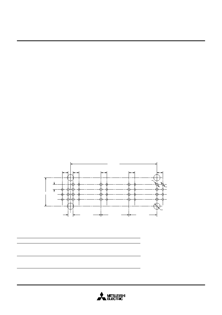
Sep.1998
6.6.5 Dead Time (t
dead
)
In order to prevent arm shoot
through a dead time between high
and low side input ON signals is
required to be included in the sys-
tem control logic. Two different val-
ues are specified on the datasheet:
A. t
dead
measured directly on
the IPM input terminals
B. t
dead
related to optocoupler
input signals using the
recommended application
circuit
The specified type B dead time is
related to standard high speed
optocouplers. (See Section 6.6.2)
By using specially selected
optocouplers with narrow distribu-
tion of switching times
the required type B dead time
could be reduced.
6.6.6 Using the Fault Signal
In order to keep the interface cir-
cuits simple the IPM uses
a single on/off output to alert the
system controller of all fault condi-
tions. The system controller can
easily determine whether the fault
signal was caused by an over tem-
perature or over current/short cir-
cuit by examining its duration.
Short circuit and over current con-
dition fault signals will be t
FO
(nominal 1.5ms) in duration. An
over temperature fault signal will be
much longer. The over temperature
Figure 6.45
PCB Layout for V-Series Connector
fault starts when the base plate
temperature exceeds the OT level
and does not reset until the base
plate cools below the OT
r
level.
Typically this takes tens of sec-
onds.
Note:
Unused fault outputs must be prop-
erly terminated by connecting them
to the +15V on the local control
power supply. Failure to properly
terminate unused fault outputs may
result in unexpected tripping of the
modules internal protection.
3 ± 0.05
3 ± 0.05
3 ± 0.05
3 ± 0.05
3 ± 0.05
43.57 ± 0.1
19 - ¯1.2
+0.1
0
19 - ¯0.9
+0.1
0
4 - ¯3.2
+0.1
-0.07
14.1 ± 0.05
14.1 ± 0.05
2.54 ± 0.05
2.54 ± 0.05
14.1 ± 0.05
14.6 ± 0.1
Table 6.8 V-Series IPM Connection Methods
V-Series Intelligent Power Module Type
Connection Method
PM75RVA060, PM100CVA060, PM150CVA060,
19 Position, 0.1" Compound
PM200CVA060, PM300CVA060, PM50RVA120,
Inverse Header Receptacle,
PM75CVA120, PM100CVA120, PM150CVA120
Hirose Part # MDF92-19S-2.54DSA
PM400DVA060, PM600DVA060,
5 Position, 0.1" (2.54mm)
PM200DVA120, PM300DVA120
Inverse Header Receptacle,
Hirose Part # MDF7-5S-2.54DSA
MITSUBISHI SEMICONDUCTORS POWER MODULES MOS
USING INTELLIGENT POWER MODULES
Sep.1998
6.7 IPM Inverter Example
The IPMs integrated intelligence
greatly simplifies inverter design.
The built in protection circuits allow
maximum utilization of power de-
vice capability without compromis-
ing reliability. Figure 6.46 shows a
complete inverter constructed us-
ing dual type IPMs. Input common
mode noise filtering and MOV
surge suppression helps to protect
the input rectifier and IPMs from
line transients. The main power
bus is constructed using laminated
plates in order to minimize parasitic
inductance. Low inductance bus
designs are covered in more detail
in Sections 3.2 and 3.3. An ex-
ample of the mechanical layout of
the inverter is shown in Figure
6.47. The IPMs must be mounted
on a heatsink with suitable cooling
capabilities. Thermal design and
power loss estimation is covered in
Section 3.4. Mitsubishi offers a
complete line-up of diode modules
that are ideal for use as the input
bridge in inverter applications.
Figure 6.46
IPM Inverter System
+
≠
RECTIFIER
BRIDGE
A
C
B
C
C
C
HEAT SINK
GROUND
IPM
+
IPM
IPM
PRINTED CIRCUIT BOARD
CONTAINING INTERFACE
CIRCUITS AND ISOLATED
POWER SUPPLIES
MICRO-CONTROLLER
PWM GENERATOR
INPUT COMMON MODE
NOISE FILTER AND MOV
SURGE PROTECTION
C
470pF STYLE 2 & 3
C
2200pF STYLE 1
MAIN
FILTER
3-PHASE INPUT
LAMINATED
BUS
STRUCTURE
U
V
W
TO LOAD (3-PHASE MOTOR)
S
SNUBBER
S
S
S
Figure 6.47
Power Circuit Layout for IPMs
CONTROL
PRINTED CIRCUIT
BOARD
SNUBBER
CIRCUIT
HEAT SINK
COPPER-INSULATOR-COPPER
SANDWICH
CAPACITOR
MITSUBISHI SEMICONDUCTORS POWER MODULES MOS
USING INTELLIGENT POWER MODULES
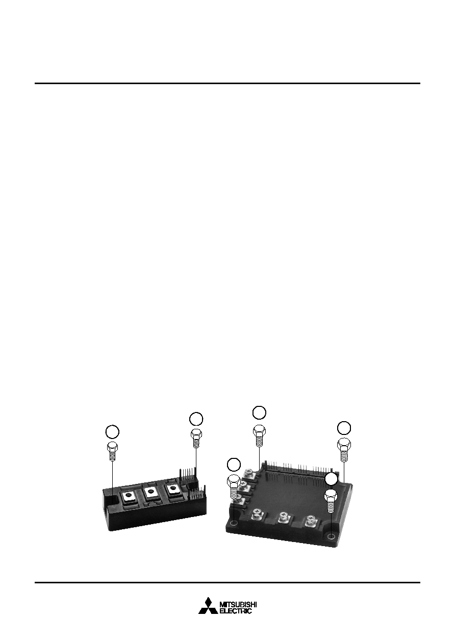
Sep.1998
6.8
Handling Precautions for
Intelligent Power Modules
Electrical Considerations:
I.
Apply proper control voltages
and input signals before static
testing.
II.
Carefully check wiring of con-
trol voltage sources and input
signals. Miswiring may destroy
the integrated gate control cir-
cuit.
III. When measuring leakage cur-
rent always ramp the curve
tracer voltage up from zero.
Ramp voltage back down be-
fore disconnecting the device.
Never apply a voltage greater
than the V
CES
rating
of the device.
IV. When measuring saturation
voltage low inductance test fix-
tures must be used. Inductive
surge voltages can exceed de-
vice ratings.
Mechanical Considerations:
I.
Avoid mechanical shock. The
module uses ceramic isolation
that can be cracked if the mod-
ule is dropped.
II.
Do not bend the power termi-
nals. Lifting or twisting the
power terminals may cause
stress cracks in the copper.
III. Do not over torque terminal or
mounting screws. Maximum
torque specifications are pro-
vided in device data sheets.
IV. Avoid uneven mounting stress.
A heatsink with a flatness of
0.001"/1" or better is recom-
mended. Avoid one sided tight-
ening stress. Figure 6.48
shows the recommended
torquing order for mounting
screws. Uneven mounting can
cause the modules ceramic
isolation to crack.
Thermal Considerations:
I.
Do not put the module on a hot
plate. Externally heating the
module's base plate at a rate
greater than 15
∞
C/min. will
cause thermal stress that may
damage the module.
II.
When soldering to the signal
pins and fast on terminals
avoid excessive heat. The sol-
dering time and temperature
should not exceed 230
∞
C for
5 seconds.
III. Maximize base plate to
heatsink contact area for good
heat transfer. Use a thermal in-
terface compound such as
white silicon grease. The
heatsink should have a surface
finish of 64 microinches or
less.
Figure 6.48
Mounting Screws Torque Order
2
1
4
1
2
3
MITSUBISHI SEMICONDUCTORS POWER MODULES MOS
USING INTELLIGENT POWER MODULES